16-channel constant-current led sink driver · 16-channel constant-current led sink drivers 2• 16...
TRANSCRIPT
1FEATURES
APPLICATIONS
DESCRIPTION/ORDERING INFORMATION
TLC5926, TLC5927
www.ti.com ....................................................................................................................................................................................................... SLVS677–JULY 2008
16-CHANNEL CONSTANT-CURRENT LED SINK DRIVERS
2• 16 Constant-Current Output Channels • 30-MHz Clock Frequency• Output Current Adjusted By External Resistor • Schmitt-Trigger Input• Constant Output Current Range: 5 mA to • 3.3-V or 5-V Supply Voltage
120 mA • Thermal Shutdown for Overtemperature• Constant Output Current Invariant to Load Protection
Voltage Change • ESD Performance: 2-kV HBM• Open-Load, Shorted-Load and
Overtemperature Detection• General LED Lighting Applications• 256-Step Programmable Global Current Gain• LED Display Systems• Excellent Output-Current Accuracy:• LED Signage– Between Channels: < ±6% (Max),• Automotive LED Lighting10 mA to 50 mA• White Goods– Between ICs: < ±6% (Max), 10 mA to 50 mA
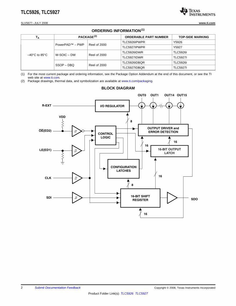
The TLC5926/TLC5927 is designed for LED displays and LED lighting applications with open-load, shorted-load,and overtemperature detection, and constant-current control. The TLC5926/TLC5927 contains a 16-bit shiftregister and data latches, which convert serial input data into parallel output format. At the TLC5926/TLC5927output stage, 16 regulated-current ports provide uniform and constant current for driving LEDs within a widerange of VF (Forward Voltage) variations. Used in systems designed for LED display applications (e.g., LEDpanels), TLC5926/TLC5927 provides great flexibility and device performance. Users can adjust the outputcurrent from 5 mA to 120 mA through an external resistor, Rext, which gives flexibility in controlling the lightintensity of LEDs. TLC5926/TLC5927 is designed for up to 17 V at the output port. The high clock frequency, 30MHz, also satisfies the system requirements of high-volume data transmission.
The TLC5926/TLC5927 provides a Special Mode in which two functions are included, Error Detection andCurrent Gain Control. In the TLC5926/TLC5927 there are two operation modes and three phases: Normal Modephase, Mode Switching transition phase, and Special mode phase. The signal on the multiple-function pinOE(ED2) is monitored, and when an one-clock-wide short pulse appears on OE(ED2), TLC5926/TLC5927 entersthe Mode Switching phase. At this time, the voltage level on LE(ED1) determines the next mode into which theTLC5926/TLC5927 switches.
In the Normal Mode phase, the serial data is transferred into TLC5926/TLC5927 via SDI, shifted in the shiftregister, and transferred out via SDO. LE(ED1) can latch the serial data in the shift register to the output latch.OE(ED2) enables the output drivers to sink current.
In the Special Mode phase, the low-voltage-level signal OE(ED2) can enable output channels and detect thestatus of the output current, to tell if the driving current level is enough or not. The detected error status is loadedinto the 16-bit shift register and shifted out via SDO, along with the CLK signal. The system controller can readthe error status to determine whether or not the LEDs are properly lit. In the Special Mode phase,TLC5926/TLC5927 also allows users to adjust the output current level by setting a runtime-programmableConfiguration Code. The code is sent into TLC5926/TLC5927 via SDI. The positive pulse of LE(ED1) latches thecode in the shift register into a built-in 8-bit configuration latch, instead of the output latch. The code affects thevoltage at R-EXT and controls the output-current regulator. The output current can be adjusted finely by a gainranging from 1/12 to 127/128 in 256 steps. Therefore, the current skew between ICs can be compensated withinless than 1%, and this feature is suitable for white balancing in LED color-display panels.
1
Please be aware that an important notice concerning availability, standard warranty, and use in critical applications of TexasInstruments semiconductor products and disclaimers thereto appears at the end of this data sheet.
2PowerPAD is a trademark of Texas Instruments.
PRODUCTION DATA information is current as of publication date. Copyright © 2008, Texas Instruments IncorporatedProducts conform to specifications per the terms of the TexasInstruments standard warranty. Production processing does notnecessarily include testing of all parameters.
SDO
VDD
R-EXT
OE(ED2)
LE(ED1)
CLK
SDI
CONTROL
LOGIC
I/O REGULATOR
CONFIGURATION
LATCHES
OUTPUT DRIVER and
ERROR DETECTION
16-BIT SHIFT
REGISTER
8
16
8
16
16
16
OUT15OUT14OUT0 OUT1
16-BIT OUTPUT
LATCH
TLC5926, TLC5927
SLVS677–JULY 2008 ....................................................................................................................................................................................................... www.ti.com
ORDERING INFORMATION (1)
TA PACKAGE (2) ORDERABLE PART NUMBER TOP-SIDE MARKINGTLC5926IPWPR Y5926
PowerPAD™ – PWP Reel of 2000TLC5927IPWPR Y5927TLC5926IDWR TLC5926I
–40°C to 85°C W-SOIC – DW Reel of 2000TLC5927IDWR TLC5927ITLC5926IDBQR TLC5926I
SSOP – DBQ Reel of 2000TLC5927IDBQR TLC5927I
(1) For the most current package and ordering information, see the Package Option Addendum at the end of this document, or see the TIweb site at www.ti.com.
(2) Package drawings, thermal data, and symbolization are available at www.ti.com/packaging.
BLOCK DIAGRAM
2 Submit Documentation Feedback Copyright © 2008, Texas Instruments Incorporated
Product Folder Link(s): TLC5926 TLC5927
1
2
3
4
5
6
7
8
9
10
11
12
24
23
22
21
20
19
18
17
16
15
14
13
GND
SDI
CLK
LE(ED1)
OUT0
OUT1
OUT2
OUT3
OUT4
OUT5
OUT6
OUT7
VDD
R-EXT
SDO
OE(ED2)
OUT15
OUT14
OUT13
OUT12
OUT11
OUT10
OUT9
OUT8
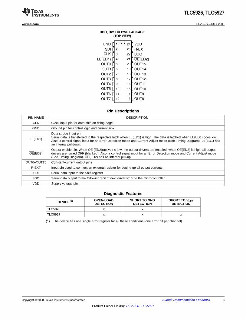
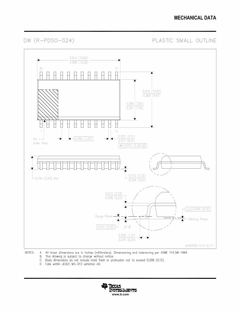
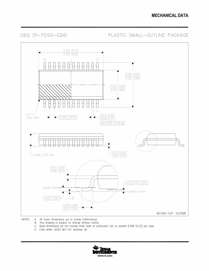
DBQ, DW, OR PWP PACKAGE
(TOP VIEW)
TLC5926, TLC5927
www.ti.com ....................................................................................................................................................................................................... SLVS677–JULY 2008
Pin DescriptionsPIN NAME DESCRIPTION
CLK Clock input pin for data shift on rising edgeGND Ground pin for control logic and current sink
Data strobe input pnSerial data is transferred to the respective latch when LE(ED1) is high. The data is latched when LE(ED1) goes low.LE(ED1) Also, a control signal input for an Error Detection mode and Current Adjust mode (See Timing Diagram). LE(ED1) hasan internal pulldown.Output enable pin. When OE (ED2)(active) is low, the output drivers are enabled; when OE(ED2) is high, all output
OE(ED2) drivers are turned OFF (blanked). Also, a control signal input for an Error Detection mode and Current Adjust mode(See Timing Diagram). OE(ED2) has an internal pull-up.
OUT0–OUT15 Constant-current output pinsR-EXT Input pin used to connect an external resistor for setting up all output currents
SDI Serial-data input to the Shift registerSDO Serial-data output to the following SDI of next driver IC or to the microcontrollerVDD Supply voltage pin
Diagnostic FeaturesOPEN-LOAD SHORT TO GND SHORT TO VLEDDEVICE (1)DETECTION DETECTION DETECTION
TLC5926 x xTLC5927 x x x
(1) The device has one single error register for all these conditions (one error bit per channel)
Copyright © 2008, Texas Instruments Incorporated Submit Documentation Feedback 3
Product Folder Link(s): TLC5926 TLC5927
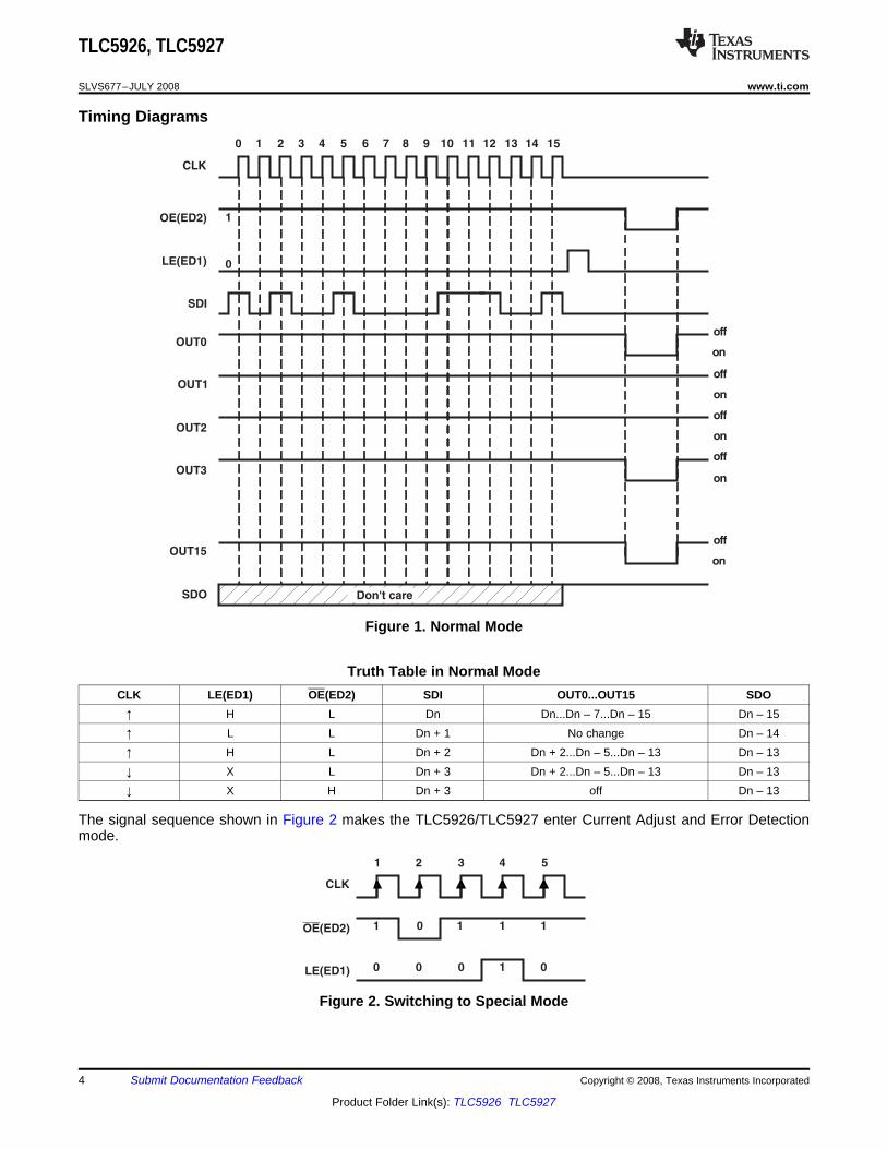
Timing Diagrams1 2 30 4 6 75 9 10 118 12 14 1513
0
1
off
on
off
on
off
on
off
on
off
on
Don't care
CLK
OE(ED2)
LE(ED1)
SDI
OUT0
OUT1
OUT2
OUT3
OUT15
SDO
1 2 3 4 5
1 0 1 1 1
10 0 0 0
CLK
OE(ED2)
LE(ED1)
TLC5926, TLC5927
SLVS677–JULY 2008 ....................................................................................................................................................................................................... www.ti.com
Figure 1. Normal Mode
Truth Table in Normal ModeCLK LE(ED1) OE(ED2) SDI OUT0...OUT15 SDO↑ H L Dn Dn...Dn – 7...Dn – 15 Dn – 15↑ L L Dn + 1 No change Dn – 14↑ H L Dn + 2 Dn + 2...Dn – 5...Dn – 13 Dn – 13↓ X L Dn + 3 Dn + 2...Dn – 5...Dn – 13 Dn – 13↓ X H Dn + 3 off Dn – 13
The signal sequence shown in Figure 2 makes the TLC5926/TLC5927 enter Current Adjust and Error Detectionmode.
Figure 2. Switching to Special Mode
4 Submit Documentation Feedback Copyright © 2008, Texas Instruments Incorporated
Product Folder Link(s): TLC5926 TLC5927
1 2 30 4 12 13 14 15
1
0
16-bit configuration code
CLK
OE(ED2)
LE(ED1)
SDI
1 2 3
0
1
>2 µs
CLK
OE(ED2)
LE(ED1)
SDO Error status code
1 2 3 4 5
1 0 1 1 1
0 0 0 00
CLK
OE(ED2)
LE(ED1)
TLC5926, TLC5927
www.ti.com ....................................................................................................................................................................................................... SLVS677–JULY 2008
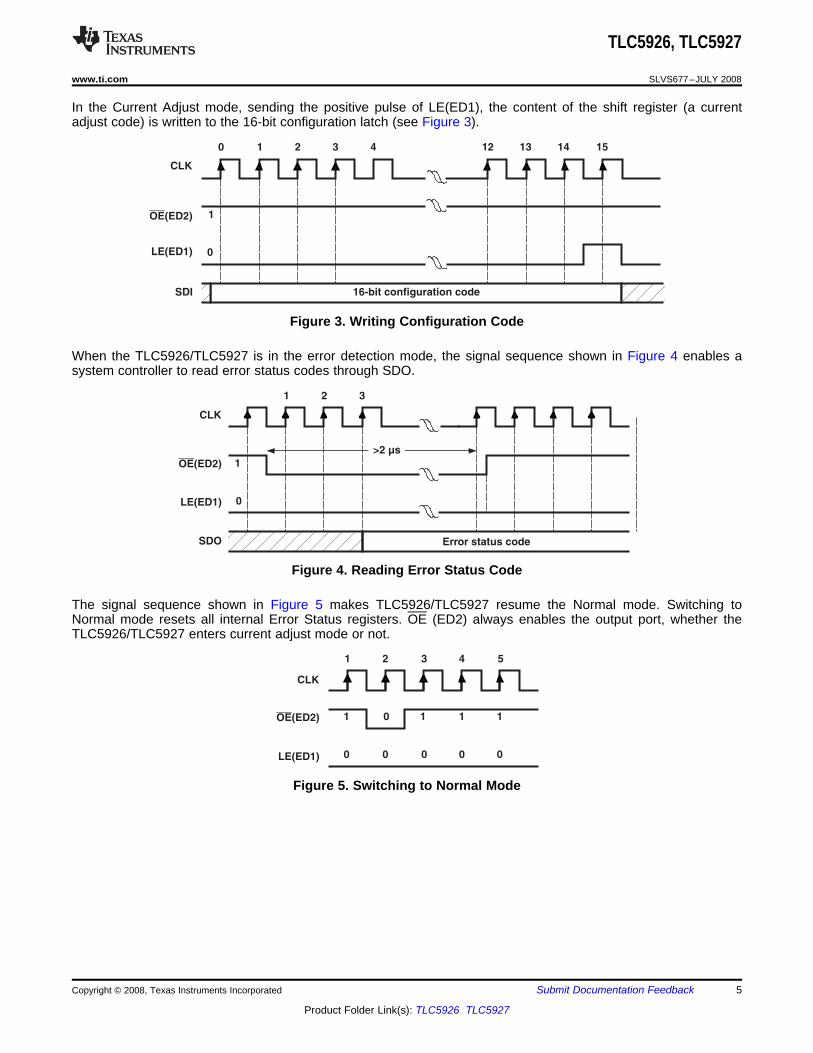
In the Current Adjust mode, sending the positive pulse of LE(ED1), the content of the shift register (a currentadjust code) is written to the 16-bit configuration latch (see Figure 3).
Figure 3. Writing Configuration Code
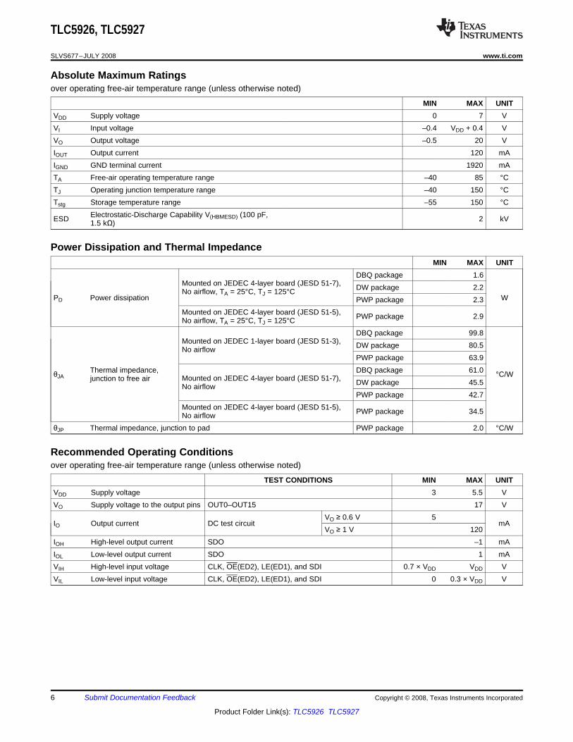
When the TLC5926/TLC5927 is in the error detection mode, the signal sequence shown in Figure 4 enables asystem controller to read error status codes through SDO.
Figure 4. Reading Error Status Code
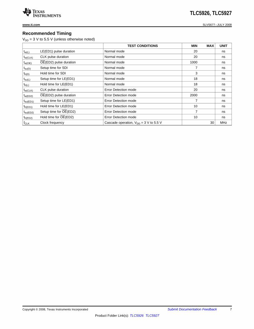
The signal sequence shown in Figure 5 makes TLC5926/TLC5927 resume the Normal mode. Switching toNormal mode resets all internal Error Status registers. OE (ED2) always enables the output port, whether theTLC5926/TLC5927 enters current adjust mode or not.
Figure 5. Switching to Normal Mode
Copyright © 2008, Texas Instruments Incorporated Submit Documentation Feedback 5
Product Folder Link(s): TLC5926 TLC5927
Absolute Maximum Ratings
Power Dissipation and Thermal Impedance
Recommended Operating Conditions
TLC5926, TLC5927
SLVS677–JULY 2008 ....................................................................................................................................................................................................... www.ti.com
over operating free-air temperature range (unless otherwise noted)
MIN MAX UNITVDD Supply voltage 0 7 VVI Input voltage –0.4 VDD + 0.4 VVO Output voltage –0.5 20 VIOUT Output current 120 mAIGND GND terminal current 1920 mATA Free-air operating temperature range –40 85 °CTJ Operating junction temperature range –40 150 °CTstg Storage temperature range –55 150 °C
Electrostatic-Discharge Capability V(HBMESD) (100 pF,ESD 2 kV1.5 kΩ)
MIN MAX UNITDBQ package 1.6
Mounted on JEDEC 4-layer board (JESD 51-7), DW package 2.2No airflow, TA = 25°C, TJ = 125°CPD Power dissipation WPWP package 2.3
Mounted on JEDEC 4-layer board (JESD 51-5), PWP package 2.9No airflow, TA = 25°C, TJ = 125°CDBQ package 99.8
Mounted on JEDEC 1-layer board (JESD 51-3), DW package 80.5No airflowPWP package 63.9
Thermal impedance, DBQ package 61.0θJA °C/WMounted on JEDEC 4-layer board (JESD 51-7),junction to free air DW package 45.5No airflowPWP package 42.7
Mounted on JEDEC 4-layer board (JESD 51-5), PWP package 34.5No airflowθJP Thermal impedance, junction to pad PWP package 2.0 °C/W
over operating free-air temperature range (unless otherwise noted)
TEST CONDITIONS MIN MAX UNITVDD Supply voltage 3 5.5 VVO Supply voltage to the output pins OUT0–OUT15 17 V
VO ≥ 0.6 V 5IO Output current DC test circuit mA
VO ≥ 1 V 120IOH High-level output current SDO –1 mAIOL Low-level output current SDO 1 mAVIH High-level input voltage CLK, OE(ED2), LE(ED1), and SDI 0.7 × VDD VDD VVIL Low-level input voltage CLK, OE(ED2), LE(ED1), and SDI 0 0.3 × VDD V
6 Submit Documentation Feedback Copyright © 2008, Texas Instruments Incorporated
Product Folder Link(s): TLC5926 TLC5927
Recommended Timing
TLC5926, TLC5927
www.ti.com ....................................................................................................................................................................................................... SLVS677–JULY 2008
VDD = 3 V to 5.5 V (unless otherwise noted)
TEST CONDITIONS MIN MAX UNITtw(L) LE(ED1) pulse duration Normal mode 20 nstw(CLK) CLK pulse duration Normal mode 20 nstw(OE) OE(ED2) pulse duration Normal mode 1000 nstsu(D) Setup time for SDI Normal mode 7 nsth(D) Hold time for SDI Normal mode 3 nstsu(L) Setup time for LE(ED1) Normal mode 18 nsth(L) Hold time for LE(ED1) Normal mode 18 nstw(CLK) CLK pulse duration Error Detection mode 20 nstw(ED2) OE(ED2) pulse duration Error Detection mode 2000 nstsu(ED1) Setup time for LE(ED1) Error Detection mode 7 nsth(ED1) Hold time for LE(ED1) Error Detection mode 10 nstsu(ED2) Setup time for OE(ED2) Error Detection mode 7 nsth(ED2) Hold time for OE(ED2) Error Detection mode 10 nsfCLK Clock frequency Cascade operation, VDD = 3 V to 5.5 V 30 MHz
Copyright © 2008, Texas Instruments Incorporated Submit Documentation Feedback 7
Product Folder Link(s): TLC5926 TLC5927
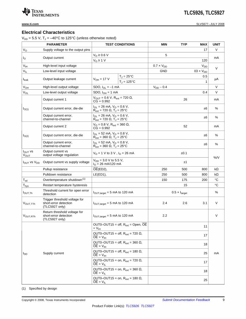
Electrical Characteristics
TLC5926, TLC5927
SLVS677–JULY 2008 ....................................................................................................................................................................................................... www.ti.com
VDD = 3 V, TJ = –40°C to 125°C (unless otherwise noted)
PARAMETER TEST CONDITIONS MIN TYP MAX UNITVO Supply voltage to the output pins 17 V
VO ≥ 0.6 V 5IO Output current mA
VO ≥ 1 V 120VIH High-level input voltage 0.7 × VDD VDD VVIL Low-level input voltage GND 0.3 × VDD
TJ = 25°C 0.5Ileak Output leakage current VOH = 17 V µA
TJ = 125°C 1VOH High-level output voltage SDO, IOL = –1 mA VDD – 0.4 VVOL Low-level output voltage SDO, IOH = 1 mA 0.4 V
VOUT = 0.6 V, Rext = 720 Ω,Output current 1 26 mACG = 0.992IOL = 26 mA, VO = 0.6 V,IO(1) Output current error, die-die ±6 %Rext = 720 Ω, TJ = 25°C
Output current error, IOL = 26 mA, VO = 0.6 V, ±6 %channel-to-channel Rext = 720 Ω, TJ = 25°CVO = 0.8 V, Rext = 360 Ω,Output current 2 52 mACG = 0.992IOL = 52 mA, VO = 0.8 V,IO(2) Output current error, die-die ±6 %Rext = 360 Ω, TJ = 25°C
Output current error, IOL = 52 mA, VO = 0.8 V, ±6 %channel-to-channel Rext = 360 Ω, TJ = 25°CIOUT vs Output current vs VO = 1 V to 3 V, IO = 26 mA ±0.1VOUT output voltage regulation
%/VVDD = 3.0 V to 5.5 V,IOUT vs VDD Output current vs supply voltage ±1IO = 26 mA/120 mA
Pullup resistance OE(ED2) 250 500 800 kΩPulldown resistance LE(ED1) 250 500 800 kΩ
Tsd Overtemperature shutdown (1) 150 175 200 °CThys Restart temperature hysteresis 15 °C
Threshold current for open errorIOUT,Th IOUT,target = 5 mA to 120 mA 0.5 × Itarget %detectionTrigger threshold voltage for
VOUT,TTh short-error detection IOUT,target = 5 mA to 120 mA 2.4 2.6 3.1 V(TLC5927 only)Return threshold voltage for
VOUT,RTh short-error detection IOUT,target = 5 mA to 120 mA 2.2 V(TLC5927 only)
OUT0–OUT15 = off, Rext = Open, OE 10= VIH
OUT0–OUT15 = off, Rext = 720 Ω, 14OE = VIH
OUT0–OUT15 = off, Rext = 360 Ω, 18OE = VIH
OUT0–OUT15 = off, Rext = 180 Ω,IDD Supply current 20 mAOE = VIH
OUT0–OUT15 = on, Rext = 720 Ω, 14OE = VIL
OUT0–OUT15 = on, Rext = 360 Ω, 18OE = VIL
OUT0–OUT15 = on, Rext = 180 Ω, 20OE = VIL
(1) Specified by design
8 Submit Documentation Feedback Copyright © 2008, Texas Instruments Incorporated
Product Folder Link(s): TLC5926 TLC5927
Electrical Characteristics
TLC5926, TLC5927
www.ti.com ....................................................................................................................................................................................................... SLVS677–JULY 2008
VDD = 5.5 V, TJ = –40°C to 125°C (unless otherwise noted)
PARAMETER TEST CONDITIONS MIN TYP MAX UNITVO Supply voltage to the output pins 17 V
VO ≥ 0.6 V 5IO Output current mA
VO ≥ 1 V 120VIH High-level input voltage 0.7 × VDD VDD VVIL Low-level input voltage GND 03 × VDD
TJ = 25°C 0.5Ileak Output leakage current VOH = 17 V µA
TJ = 125°C 1VOH High-level output voltage SDO, IOL = –1 mA VDD – 0.4 VVOL Low-level output voltage SDO, IOH = 1 mA 0.4 V
VOUT = 0.6 V, Rext = 720 Ω,Output current 1 26 mACG = 0.992IOL = 26 mA, VO = 0.6 V,IO(1) Output current error, die-die ±6 %Rext = 720 Ω, TJ = 25°C
Output current error, IOL = 26 mA, VO = 0.6 V, ±6 %channel-to-channel Rext = 720 Ω, TJ = 25°CVO = 0.8 V, Rext = 360 Ω,Output current 2 52 mACG = 0.992IOL = 52 mA, VO = 0.8 V,IO(2) Output current error, die-die ±6 %Rext = 360 Ω, TJ = 25°C
Output current error, IOL = 52 mA, VO = 0.8 V, ±6 %channel-to-channel Rext = 360 Ω, TJ = 25°CIOUT vs Output current vs VO = 1 V to 3 V , IO = 26 mA ±0.1VOUT output voltage regulation
%/VVDD = 3.0 V to 5.5 V,IOUT vs VDD Output current vs supply voltage ±1IO = 26 mA/120 mA
Pullup resistance OE(ED2), 250 500 800 kΩPulldown resistance LE(ED1), 250 500 800 kΩ
Tsd Overtemperature shutdown (1) 150 175 200 °CThys Restart temperature hysteresis 15 °C
Threshold current for open errorIOUT,Th IOUT,target = 5 mA to 120 mA 0.5 × Itarget %detectionTrigger threshold voltage for
VOUT,TTh short-error detection IOUT,target = 5 mA to 120 mA 2.4 2.6 3.1 V(TLC5927 only)Return threshold voltage for
VOUT,RTh short-error detection IOUT,target = 5 mA to 120 mA 2.2 V(TLC5927 only)
OUT0–OUT15 = off, Rext = Open, OE 11= VIH
OUT0–OUT15 = off, Rext = 720 Ω, 17OE = VIH
OUT0–OUT15 = off, Rext = 360 Ω, 18OE = VIH
OUT0–OUT15 = off, Rext = 180 Ω,IDD Supply current 25 mAOE = VIH
OUT0–OUT15 = on, Rext = 720 Ω, 17OE = VIL
OUT0–OUT15 = on, Rext = 360 Ω, 18OE = VIL
OUT0–OUT15 = on, Rext = 180 Ω, 25OE = VIL
(1) Specified by design
Copyright © 2008, Texas Instruments Incorporated Submit Documentation Feedback 9
Product Folder Link(s): TLC5926 TLC5927
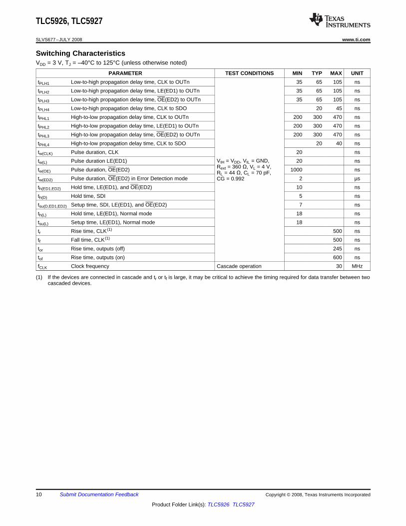
Switching Characteristics
TLC5926, TLC5927
SLVS677–JULY 2008 ....................................................................................................................................................................................................... www.ti.com
VDD = 3 V, TJ = –40°C to 125°C (unless otherwise noted)
PARAMETER TEST CONDITIONS MIN TYP MAX UNITtPLH1 Low-to-high propagation delay time, CLK to OUTn 35 65 105 nstPLH2 Low-to-high propagation delay time, LE(ED1) to OUTn 35 65 105 nstPLH3 Low-to-high propagation delay time, OE(ED2) to OUTn 35 65 105 nstPLH4 Low-to-high propagation delay time, CLK to SDO 20 45 nstPHL1 High-to-low propagation delay time, CLK to OUTn 200 300 470 nstPHL2 High-to-low propagation delay time, LE(ED1) to OUTn 200 300 470 nstPHL3 High-to-low propagation delay time, OE(ED2) to OUTn 200 300 470 nstPHL4 High-to-low propagation delay time, CLK to SDO 20 40 nstw(CLK) Pulse duration, CLK 20 ns
VIH = VDD, VIL = GND,tw(L) Pulse duration LE(ED1) 20 nsRext = 360 Ω, VL = 4 V,tw(OE) Pulse duration, OE(ED2) 1000 nsRL = 44 Ω, CL = 70 pF,
tw(ED2) Pulse duration, OE(ED2) in Error Detection mode 2 µsCG = 0.992th(ED1,ED2) Hold time, LE(ED1), and OE(ED2) 10 nsth(D) Hold time, SDI 5 nstsu(D,ED1,ED2) Setup time, SDI, LE(ED1), and OE(ED2) 7 nsth(L) Hold time, LE(ED1), Normal mode 18 nstsu(L) Setup time, LE(ED1), Normal mode 18 nstr Rise time, CLK (1) 500 nstf Fall time, CLK (1) 500 nstor Rise time, outputs (off) 245 nstof Rise time, outputs (on) 600 nsfCLK Clock frequency Cascade operation 30 MHz
(1) If the devices are connected in cascade and tr or tf is large, it may be critical to achieve the timing required for data transfer between twocascaded devices.
10 Submit Documentation Feedback Copyright © 2008, Texas Instruments Incorporated
Product Folder Link(s): TLC5926 TLC5927
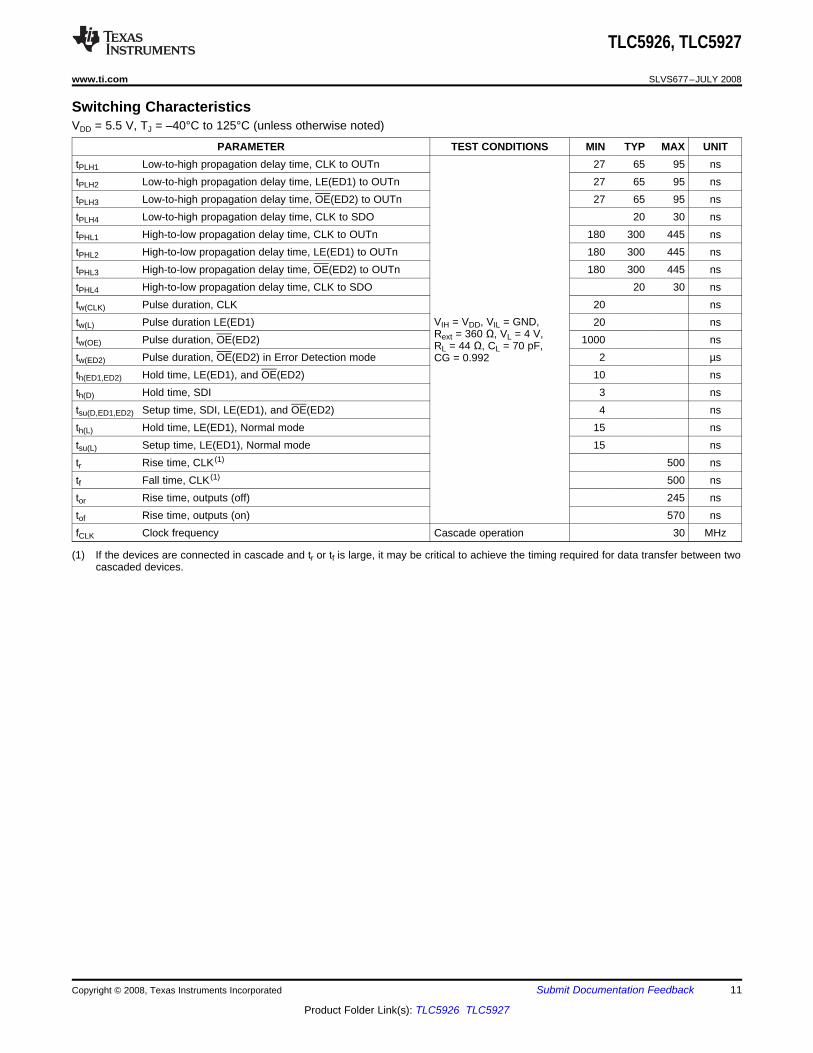
Switching Characteristics
TLC5926, TLC5927
www.ti.com ....................................................................................................................................................................................................... SLVS677–JULY 2008
VDD = 5.5 V, TJ = –40°C to 125°C (unless otherwise noted)
PARAMETER TEST CONDITIONS MIN TYP MAX UNITtPLH1 Low-to-high propagation delay time, CLK to OUTn 27 65 95 nstPLH2 Low-to-high propagation delay time, LE(ED1) to OUTn 27 65 95 nstPLH3 Low-to-high propagation delay time, OE(ED2) to OUTn 27 65 95 nstPLH4 Low-to-high propagation delay time, CLK to SDO 20 30 nstPHL1 High-to-low propagation delay time, CLK to OUTn 180 300 445 nstPHL2 High-to-low propagation delay time, LE(ED1) to OUTn 180 300 445 nstPHL3 High-to-low propagation delay time, OE(ED2) to OUTn 180 300 445 nstPHL4 High-to-low propagation delay time, CLK to SDO 20 30 nstw(CLK) Pulse duration, CLK 20 ns
VIH = VDD, VIL = GND,tw(L) Pulse duration LE(ED1) 20 nsRext = 360 Ω, VL = 4 V,tw(OE) Pulse duration, OE(ED2) 1000 nsRL = 44 Ω, CL = 70 pF,
tw(ED2) Pulse duration, OE(ED2) in Error Detection mode 2 µsCG = 0.992th(ED1,ED2) Hold time, LE(ED1), and OE(ED2) 10 nsth(D) Hold time, SDI 3 nstsu(D,ED1,ED2) Setup time, SDI, LE(ED1), and OE(ED2) 4 nsth(L) Hold time, LE(ED1), Normal mode 15 nstsu(L) Setup time, LE(ED1), Normal mode 15 nstr Rise time, CLK (1) 500 nstf Fall time, CLK (1) 500 nstor Rise time, outputs (off) 245 nstof Rise time, outputs (on) 570 nsfCLK Clock frequency Cascade operation 30 MHz
(1) If the devices are connected in cascade and tr or tf is large, it may be critical to achieve the timing required for data transfer between twocascaded devices.
Copyright © 2008, Texas Instruments Incorporated Submit Documentation Feedback 11
Product Folder Link(s): TLC5926 TLC5927
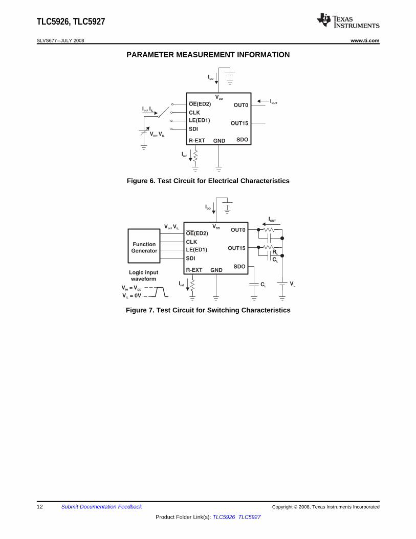
PARAMETER MEASUREMENT INFORMATION
IDD
I , IIH IL
V , VIH IL
Iref
IOUT
VDD
OE(ED2)
CLK
LE(ED1)
SDI
R-EXT GND SDO
OUT15
OUT0
V , VIH IL
Logic inputwaveform
V = VIH DD
V = 0VIL
IOUT
RL
CL
Iref
VDD
OE(ED2)
CLK
LE(ED1)
SDI
R-EXT GNDSDO
OUT15
OUT0
IDD
FunctionGenerator
VLCL
TLC5926, TLC5927
SLVS677–JULY 2008 ....................................................................................................................................................................................................... www.ti.com
Figure 6. Test Circuit for Electrical Characteristics
Figure 7. Test Circuit for Switching Characteristics
12 Submit Documentation Feedback Copyright © 2008, Texas Instruments Incorporated
Product Folder Link(s): TLC5926 TLC5927
50%
50%
LOW
Out fput of
Outp t onut , tPLH1 PHL1
t , tLH2 H 2P LP
CLK
SDI
SDO
LE(ED1)
OE(ED2)
OUTn
t , tPLH4 PHL4
tw(CLK)
50% 50%
50%
50%
50%
50%
tsu(L)th(L)
tw(L)
tsu(D) th(D)
50%
tw(OE)
tPHL3
tof tor
Output off
tPLH3
50%
10%
90%
OE(ED2)
OUTn 50%
90%
50%10%
HIGH
OE
Lo
wO
EP
uls
ed
TLC5926, TLC5927
www.ti.com ....................................................................................................................................................................................................... SLVS677–JULY 2008
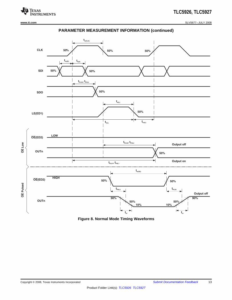
PARAMETER MEASUREMENT INFORMATION (continued)
Figure 8. Normal Mode Timing Waveforms
Copyright © 2008, Texas Instruments Incorporated Submit Documentation Feedback 13
Product Folder Link(s): TLC5926 TLC5927
tw(CLK)
tsu(ED2) th(ED2)
OE(ED2)
LE(ED1)
CLK
tsu(ED1) th(ED1)
2 CLK
50%
50%
50%
50%
50%
tw(ED2)
OE(ED2)
CLK
TLC5926, TLC5927
SLVS677–JULY 2008 ....................................................................................................................................................................................................... www.ti.com
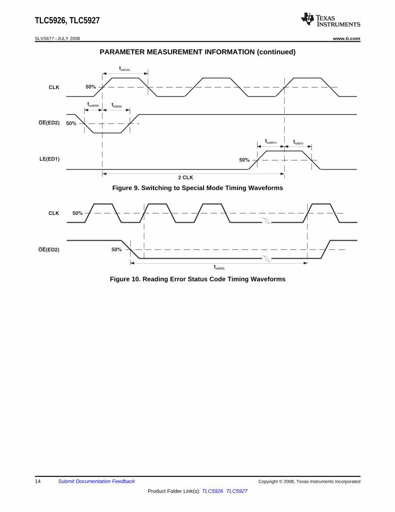
PARAMETER MEASUREMENT INFORMATION (continued)
Figure 9. Switching to Special Mode Timing Waveforms
Figure 10. Reading Error Status Code Timing Waveforms
14 Submit Documentation Feedback Copyright © 2008, Texas Instruments Incorporated
Product Folder Link(s): TLC5926 TLC5927
APPLICATION INFORMATION
Operating Principles
Constant Current
Adjusting Output Current
140
120
80
40
0
0 500 1000 1500 2000 2500 3000 3500 4000
R –ext
W
I– m
AO
UT
100
TLC5926, TLC5927
www.ti.com ....................................................................................................................................................................................................... SLVS677–JULY 2008
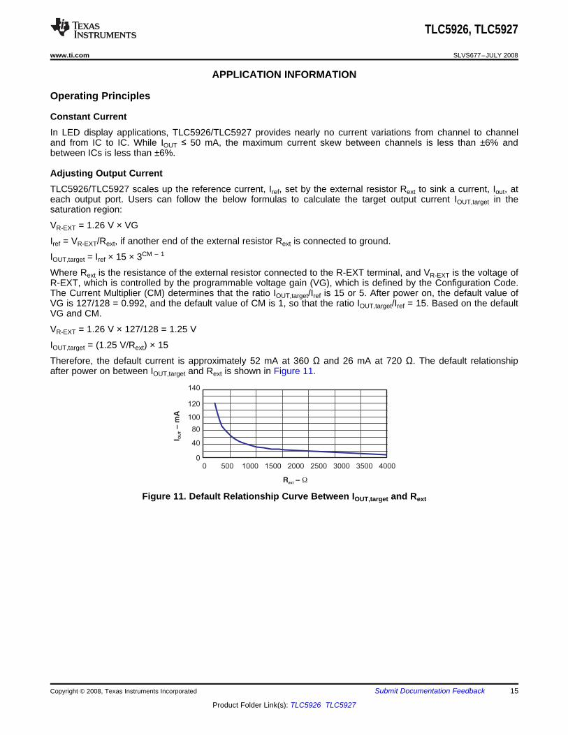
In LED display applications, TLC5926/TLC5927 provides nearly no current variations from channel to channeland from IC to IC. While IOUT ≤ 50 mA, the maximum current skew between channels is less than ±6% andbetween ICs is less than ±6%.
TLC5926/TLC5927 scales up the reference current, Iref, set by the external resistor Rext to sink a current, Iout, ateach output port. Users can follow the below formulas to calculate the target output current IOUT,target in thesaturation region:
VR-EXT = 1.26 V × VG
Iref = VR-EXT/Rext, if another end of the external resistor Rext is connected to ground.
IOUT,target = Iref × 15 × 3CM – 1
Where Rext is the resistance of the external resistor connected to the R-EXT terminal, and VR-EXT is the voltage ofR-EXT, which is controlled by the programmable voltage gain (VG), which is defined by the Configuration Code.The Current Multiplier (CM) determines that the ratio IOUT,target/Iref is 15 or 5. After power on, the default value ofVG is 127/128 = 0.992, and the default value of CM is 1, so that the ratio IOUT,target/Iref = 15. Based on the defaultVG and CM.
VR-EXT = 1.26 V × 127/128 = 1.25 V
IOUT,target = (1.25 V/Rext) × 15
Therefore, the default current is approximately 52 mA at 360 Ω and 26 mA at 720 Ω. The default relationshipafter power on between IOUT,target and Rext is shown in Figure 11.
Figure 11. Default Relationship Curve Between IOUT,target and Rext
Copyright © 2008, Texas Instruments Incorporated Submit Documentation Feedback 15
Product Folder Link(s): TLC5926 TLC5927
Operation Phases
Operation Mode Switching
1 2 3 4 5
1 0 1 1 1
00 0 0 0
Actual Mode(Normal or Special)
ModeSwitching
NormalMode
CLK
OE(ED2)
LE(ED1)
Phase
1 2 3 4 5
1 0 1 1 1
10 0 0 0
Actual Mode(Normal or Special)
ModeSwitching
SpecialMode
CLK
OE(ED2)
LE(ED1)
Phase
Switching to Special Mode Switching to Normal Mode
Normal Mode Phase
Special Mode Phase
TLC5926, TLC5927
SLVS677–JULY 2008 ....................................................................................................................................................................................................... www.ti.com
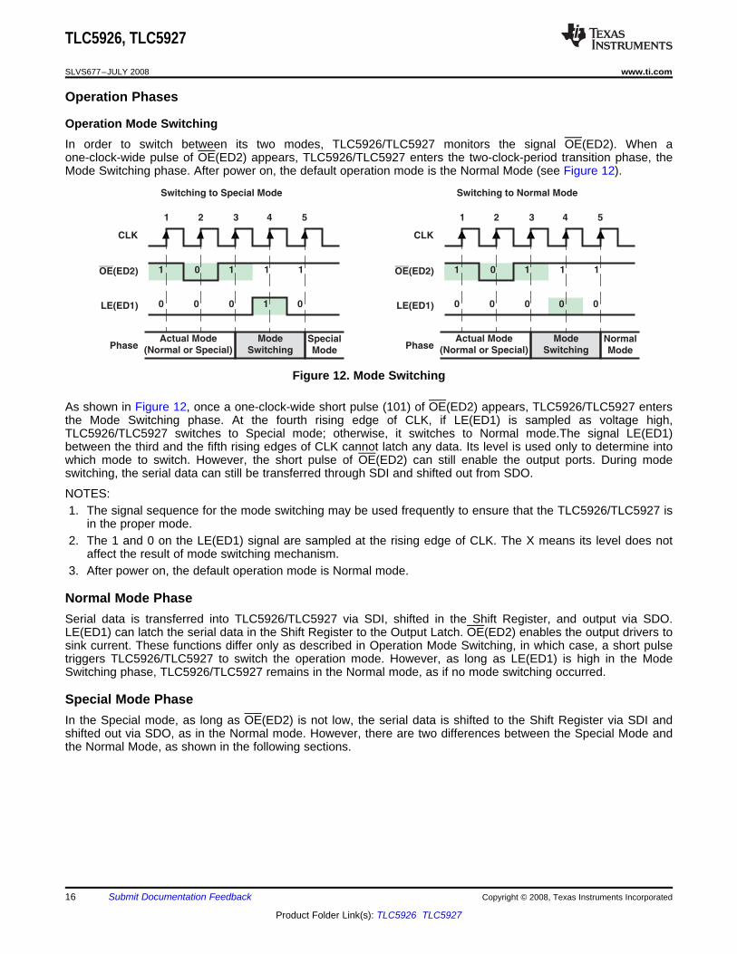
In order to switch between its two modes, TLC5926/TLC5927 monitors the signal OE(ED2). When aone-clock-wide pulse of OE(ED2) appears, TLC5926/TLC5927 enters the two-clock-period transition phase, theMode Switching phase. After power on, the default operation mode is the Normal Mode (see Figure 12).
Figure 12. Mode Switching
As shown in Figure 12, once a one-clock-wide short pulse (101) of OE(ED2) appears, TLC5926/TLC5927 entersthe Mode Switching phase. At the fourth rising edge of CLK, if LE(ED1) is sampled as voltage high,TLC5926/TLC5927 switches to Special mode; otherwise, it switches to Normal mode.The signal LE(ED1)between the third and the fifth rising edges of CLK cannot latch any data. Its level is used only to determine intowhich mode to switch. However, the short pulse of OE(ED2) can still enable the output ports. During modeswitching, the serial data can still be transferred through SDI and shifted out from SDO.
NOTES:1. The signal sequence for the mode switching may be used frequently to ensure that the TLC5926/TLC5927 is
in the proper mode.2. The 1 and 0 on the LE(ED1) signal are sampled at the rising edge of CLK. The X means its level does not
affect the result of mode switching mechanism.3. After power on, the default operation mode is Normal mode.
Serial data is transferred into TLC5926/TLC5927 via SDI, shifted in the Shift Register, and output via SDO.LE(ED1) can latch the serial data in the Shift Register to the Output Latch. OE(ED2) enables the output drivers tosink current. These functions differ only as described in Operation Mode Switching, in which case, a short pulsetriggers TLC5926/TLC5927 to switch the operation mode. However, as long as LE(ED1) is high in the ModeSwitching phase, TLC5926/TLC5927 remains in the Normal mode, as if no mode switching occurred.
In the Special mode, as long as OE(ED2) is not low, the serial data is shifted to the Shift Register via SDI andshifted out via SDO, as in the Normal mode. However, there are two differences between the Special Mode andthe Normal Mode, as shown in the following sections.
16 Submit Documentation Feedback Copyright © 2008, Texas Instruments Incorporated
Product Folder Link(s): TLC5926 TLC5927
Reading Error Status Code in Special Mode
1 2 3
1 0 0 0 1
0 0 0 00
0 0
0 0 0 0
1 1 1
0
CLK
OE(ED2)
LE(ED1)
SDO
Data source ofshift register
Error DetectionSDI SDI
Error Status Code
Bit 15 Bit 14 Bit 13 Bit 12
>2 µs
Writing Configuration Code in Special Mode
1 2 30 4 12 13 14 15
1
0
CLK
OE(ED2)
LE(ED1)
SDI16-Bit Configuration Code
Bit 15 Bit 14 Bit 13 Bit 12 Bit 3 Bit 2 Bit 1 Bit 0
TLC5926, TLC5927
www.ti.com ....................................................................................................................................................................................................... SLVS677–JULY 2008
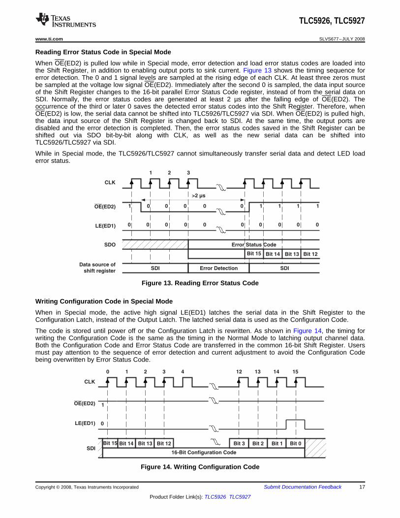
When OE(ED2) is pulled low while in Special mode, error detection and load error status codes are loaded intothe Shift Register, in addition to enabling output ports to sink current. Figure 13 shows the timing sequence forerror detection. The 0 and 1 signal levels are sampled at the rising edge of each CLK. At least three zeros mustbe sampled at the voltage low signal OE(ED2). Immediately after the second 0 is sampled, the data input sourceof the Shift Register changes to the 16-bit parallel Error Status Code register, instead of from the serial data onSDI. Normally, the error status codes are generated at least 2 µs after the falling edge of OE(ED2). Theoccurrence of the third or later 0 saves the detected error status codes into the Shift Register. Therefore, whenOE(ED2) is low, the serial data cannot be shifted into TLC5926/TLC5927 via SDI. When OE(ED2) is pulled high,the data input source of the Shift Register is changed back to SDI. At the same time, the output ports aredisabled and the error detection is completed. Then, the error status codes saved in the Shift Register can beshifted out via SDO bit-by-bit along with CLK, as well as the new serial data can be shifted intoTLC5926/TLC5927 via SDI.
While in Special mode, the TLC5926/TLC5927 cannot simultaneously transfer serial data and detect LED loaderror status.
Figure 13. Reading Error Status Code
When in Special mode, the active high signal LE(ED1) latches the serial data in the Shift Register to theConfiguration Latch, instead of the Output Latch. The latched serial data is used as the Configuration Code.
The code is stored until power off or the Configuration Latch is rewritten. As shown in Figure 14, the timing forwriting the Configuration Code is the same as the timing in the Normal Mode to latching output channel data.Both the Configuration Code and Error Status Code are transferred in the common 16-bit Shift Register. Usersmust pay attention to the sequence of error detection and current adjustment to avoid the Configuration Codebeing overwritten by Error Status Code.
Figure 14. Writing Configuration Code
Copyright © 2008, Texas Instruments Incorporated Submit Documentation Feedback 17
Product Folder Link(s): TLC5926 TLC5927
Open-Circuit Detection Principle
Short-Circuit Detection Principle (TLC5927 Only)
Overtemperature Detection and Shutdown
TLC5926, TLC5927
SLVS677–JULY 2008 ....................................................................................................................................................................................................... www.ti.com
The LED Open-Circuit Detection compares the effective current level IOUT with the open load detection thresholdcurrent IOUT,Th. If IOUT is below the IOUT,Th threshold, the TLC5926/TLC5927 detects an open-load condition. Thiserror status can be read as an error status code in the Special mode. For open-circuit error detection, a channelmust be on.
Table 1. Open-Circuit DetectionCONDITION OFSTATE OF OUTPUT PORT ERROR STATUS CODE MEANINGOUTPUT CURRENT
Off IOUT = 0 mA 0 Detection not possibleIOUT < IOUT,Th
(1) 0 Open circuitOn
IOUT ≥ IOUT,Th(1) Channel n error status bit 1 Normal
(1) IOUT,Th = 0.5 × IOUT,target (typical)
The LED short-circuit detection compares the effective voltage level VOUT with the shorted-load detectionthreshold voltages VOUT,TTh and VOUT,RTh. If VOUT is above the VOUT,TTh threshold, the TLC5927 detects anshorted-load condition. If the VOUT is below VOUT,RTh threshold, no error is detected and the error bit is reset. Thiserror status can be read as an error status code in the Special mode. For short-circuit error detection, a channelmust be on.
Table 2. Short-Circuit DetectionCONDITION OFSTATE OF OUTPUT PORT ERROR STATUS CODE MEANINGOUTPUT VOLTAGE
Off IOUT = 0 mA 0 Detection not possibleVOUT < VOUT,TTh
(1) 0 Short circuitOn
VOUT < VOUT,RTh(1) Channel n error status bit 1 Normal
(1) IOUT,Th = 0.5 × IOUT,target (typical)
The TLC5926/TLC5927 is equipped with a global overtemperature sensor and 16 individual, channel-specificovertemperature sensors.• When the global sensor reaches the trip temperature, all output channels are shutdown, and the error status
is stored in the internal Error Status register of every channel. After shutdown, the channels automaticallyrestart after cooling down, if the control signal (output latch) remains on. The stored error status is not resetafter cooling down and can be read out as the error status code in the Special mode.
• When one of the channel-specific sensors reaches trip temperature, only the affected output channel is shutdown, and the error status is stored only in the internal Error Status register of the affected channel. Aftershutdown, the channel automatically restarts after cooling down, if the control signal (output latch) remainson. The stored error status is not reset after cooling down and can be read out as error status code in theSpecial mode.
For channel-specific overtemperature error detection, a channel must be on.
The error status code is reset when the TLC5926/TLC5927 returns to Normal mode.
18 Submit Documentation Feedback Copyright © 2008, Texas Instruments Incorporated
Product Folder Link(s): TLC5926 TLC5927
16-Bit Configuration Code and Current Gain
TLC5926, TLC5927
www.ti.com ....................................................................................................................................................................................................... SLVS677–JULY 2008
Table 3. Overtemperature Detection (1)
STATE OF OUTPUT PORT CONDITION ERROR STATUS CODE MEANINGOff IOUT = 0 mA 0On Tj < Tj,trip global 1 Normal
On → all channelsTj > Tj,trip global All error status bits = 0 Global overtemperatureOff
Tj < Tj,trip channel n 1 NormalOnOn → Off Tj > Tj,trip channel n Channel n error status bit = 0 Channel n overtemperature
(1) The global shutdown threshold temperature is approximately 170°C.
Bit definition of the Configuration Code in the Configuration Latch is shown in Table 4.
Table 4. Bit Definition of 8-Bit Configuration CodeBit 0 Bit 1 Bit 2 Bit 3 Bit 4 Bit 5 Bit 6 Bit 7 Bit 8–15
Meaning CM HC CC0 CC1 CC2 CC3 CC4 CC5 Don't careDefault 1 1 1 1 1 1 1 1 X
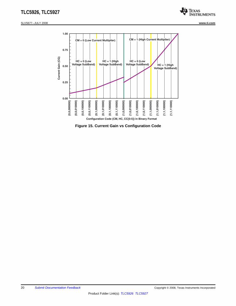
Bit 7 is first sent into TLC5926/TLC5927 via SDI. Bits 1 to 7 HC, CC[0:5] determine the voltage gain (VG) thataffects the voltage at R-EXT and indirectly affects the reference current, Iref, flowing through the external resistorat R-EXT. Bit 0 is the Current Multiplier (CM) that determines the ratio IOUT,target/Iref. Each combination of VG andCM gives a specific Current Gain (CG).• VG: the relationship between HC,CC[0:5] and the voltage gain is calculated as shown below:
VG = (1 + HC) × (1 + D/64) / 4D = CC0 × 25 + CC1 × 24 + CC2 × 23 + CC3 × 22 + CC4 × 21 + CC5 × 20
Where HC is 1 or 0, and D is the binary value of CC[0:5]. So, the VG could be regarded as a floating-pointnumber with 1-bit exponent HC and 6-bit mantissa CC[0:5]. HC,CC[0:5] divides the programmable voltagegain VG into 128 steps and two sub-bands:Low voltage sub-band (HC = 0): VG = 1/4 ~ 127/256, linearly divided into 64 stepsHigh voltage sub-band (HC = 1): VG = 1/2 ~ 127/128, linearly divided into 64 steps
• CM: In addition to determining the ratio IOUT,target/Iref, CM limits the output current range.High Current Multiplier (CM = 1): IOUT,target/Iref = 15, suitable for output current range IOUT = 10 mA to 120 mA.Low Current Multiplier (CM = 0): IOUT,target/Iref = 5, suitable for output current range IOUT = 5 mA to 40 mA
• CG: The total Current Gain is defined as the following.VR-EXT = 1.26 V × VGIref = VR-EXT/Rext, if the external resistor, Rext, is connected to ground.IOUT,target = Iref × 15 × 3CM – 1 = 1.26 V/Rext × VG × 15 × 3CM – 1 = (1.26 V/Rext × 15) × CGCG = VG × 3CM – 1
Therefore, CG = (1/12) to (127/128) divided into 256 steps.
Examples• Configuration Code CM, HC, CC[0:5] = 1,1,111111
VG = 127/128 = 0.992 and CG = VG × 30 = VG = 0.992• Configuration Code = 1,1,000000
VG = (1 + 1) × (1 + 0/64)/4 = 1/2 = 0.5, and CG = 0.5• Configuration Code = 0,0,000000
VG = (1 + 0) × (1 + 0/64)/4 = 1/4, and CG = (1/4) × 3–1 = 1/12
After power on, the default value of the Configuration Code CM, HC, CC[0:5] is 1,1,111111. Therefore,VG = CG = 0.992. The relationship between the Configuration Code and the Current Gain is shown in Figure 15.
Copyright © 2008, Texas Instruments Incorporated Submit Documentation Feedback 19
Product Folder Link(s): TLC5926 TLC5927
1.00
0.00
0.50
0.25
0.75
Configuration Code (CM, HC, CC[0:5]) in Binary Format
Cu
rren
t G
ain
(C
G)
0,0
,000000
0,0
,010000
0,0
,100000
0,0
,110000
0,1
,000000
0,1
,010000
0,1
,100000
0,1
,110000
1,0
,000000
1,0
,010000
1,0
,100000
1,0
,110000
1,1
,100000
1,1
,110000
1,1
,000000
1,1
,010000
CM = 0 (Low Current Multiplier)
HC = 1 (HighVoltage SubBand)
HC = 0 (LowVoltage SubBand) HC = 1 (High
Voltage SubBand)
CM = 1 (High Current Multiplier)
HC = 0 (LowVoltage SubBand)
TLC5926, TLC5927
SLVS677–JULY 2008 ....................................................................................................................................................................................................... www.ti.com
Figure 15. Current Gain vs Configuration Code
20 Submit Documentation Feedback Copyright © 2008, Texas Instruments Incorporated
Product Folder Link(s): TLC5926 TLC5927
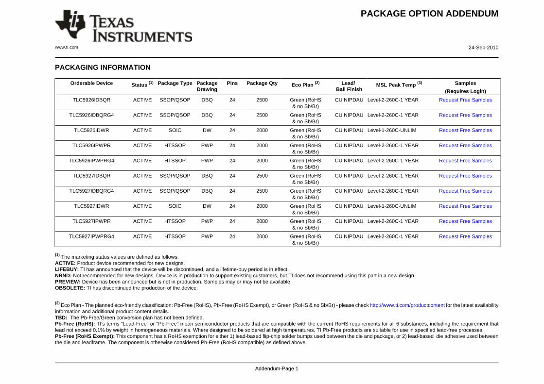
PACKAGE OPTION ADDENDUM
www.ti.com 24-Sep-2010
Addendum-Page 1
PACKAGING INFORMATION
Orderable Device Status (1) Package Type PackageDrawing
Pins Package Qty Eco Plan (2) Lead/Ball Finish
MSL Peak Temp (3) Samples
(Requires Login)
TLC5926IDBQR ACTIVE SSOP/QSOP DBQ 24 2500 Green (RoHS& no Sb/Br)
CU NIPDAU Level-2-260C-1 YEAR Request Free Samples
TLC5926IDBQRG4 ACTIVE SSOP/QSOP DBQ 24 2500 Green (RoHS& no Sb/Br)
CU NIPDAU Level-2-260C-1 YEAR Request Free Samples
TLC5926IDWR ACTIVE SOIC DW 24 2000 Green (RoHS& no Sb/Br)
CU NIPDAU Level-1-260C-UNLIM Request Free Samples
TLC5926IPWPR ACTIVE HTSSOP PWP 24 2000 Green (RoHS& no Sb/Br)
CU NIPDAU Level-2-260C-1 YEAR Request Free Samples
TLC5926IPWPRG4 ACTIVE HTSSOP PWP 24 2000 Green (RoHS& no Sb/Br)
CU NIPDAU Level-2-260C-1 YEAR Request Free Samples
TLC5927IDBQR ACTIVE SSOP/QSOP DBQ 24 2500 Green (RoHS& no Sb/Br)
CU NIPDAU Level-2-260C-1 YEAR Request Free Samples
TLC5927IDBQRG4 ACTIVE SSOP/QSOP DBQ 24 2500 Green (RoHS& no Sb/Br)
CU NIPDAU Level-2-260C-1 YEAR Request Free Samples
TLC5927IDWR ACTIVE SOIC DW 24 2000 Green (RoHS& no Sb/Br)
CU NIPDAU Level-1-260C-UNLIM Request Free Samples
TLC5927IPWPR ACTIVE HTSSOP PWP 24 2000 Green (RoHS& no Sb/Br)
CU NIPDAU Level-2-260C-1 YEAR Request Free Samples
TLC5927IPWPRG4 ACTIVE HTSSOP PWP 24 2000 Green (RoHS& no Sb/Br)
CU NIPDAU Level-2-260C-1 YEAR Request Free Samples
(1) The marketing status values are defined as follows:ACTIVE: Product device recommended for new designs.LIFEBUY: TI has announced that the device will be discontinued, and a lifetime-buy period is in effect.NRND: Not recommended for new designs. Device is in production to support existing customers, but TI does not recommend using this part in a new design.PREVIEW: Device has been announced but is not in production. Samples may or may not be available.OBSOLETE: TI has discontinued the production of the device.
(2) Eco Plan - The planned eco-friendly classification: Pb-Free (RoHS), Pb-Free (RoHS Exempt), or Green (RoHS & no Sb/Br) - please check http://www.ti.com/productcontent for the latest availabilityinformation and additional product content details.TBD: The Pb-Free/Green conversion plan has not been defined.Pb-Free (RoHS): TI's terms "Lead-Free" or "Pb-Free" mean semiconductor products that are compatible with the current RoHS requirements for all 6 substances, including the requirement thatlead not exceed 0.1% by weight in homogeneous materials. Where designed to be soldered at high temperatures, TI Pb-Free products are suitable for use in specified lead-free processes.Pb-Free (RoHS Exempt): This component has a RoHS exemption for either 1) lead-based flip-chip solder bumps used between the die and package, or 2) lead-based die adhesive used betweenthe die and leadframe. The component is otherwise considered Pb-Free (RoHS compatible) as defined above.
PACKAGE OPTION ADDENDUM
www.ti.com 24-Sep-2010
Addendum-Page 2
Green (RoHS & no Sb/Br): TI defines "Green" to mean Pb-Free (RoHS compatible), and free of Bromine (Br) and Antimony (Sb) based flame retardants (Br or Sb do not exceed 0.1% by weightin homogeneous material)
(3) MSL, Peak Temp. -- The Moisture Sensitivity Level rating according to the JEDEC industry standard classifications, and peak solder temperature.
Important Information and Disclaimer:The information provided on this page represents TI's knowledge and belief as of the date that it is provided. TI bases its knowledge and belief on informationprovided by third parties, and makes no representation or warranty as to the accuracy of such information. Efforts are underway to better integrate information from third parties. TI has taken andcontinues to take reasonable steps to provide representative and accurate information but may not have conducted destructive testing or chemical analysis on incoming materials and chemicals.TI and TI suppliers consider certain information to be proprietary, and thus CAS numbers and other limited information may not be available for release.
In no event shall TI's liability arising out of such information exceed the total purchase price of the TI part(s) at issue in this document sold by TI to Customer on an annual basis.
OTHER QUALIFIED VERSIONS OF TLC5926, TLC5927 :
• Automotive: TLC5926-Q1, TLC5927-Q1
NOTE: Qualified Version Definitions:
• Automotive - Q100 devices qualified for high-reliability automotive applications targeting zero defects
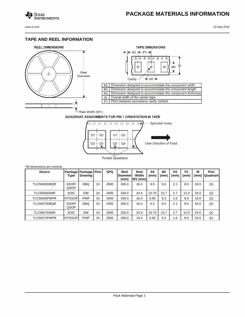
TAPE AND REEL INFORMATION
*All dimensions are nominal
Device PackageType
PackageDrawing
Pins SPQ ReelDiameter
(mm)
ReelWidth
W1 (mm)
A0(mm)
B0(mm)
K0(mm)
P1(mm)
W(mm)
Pin1Quadrant
TLC5926IDBQR SSOP/QSOP
DBQ 24 2500 330.0 16.4 6.5 9.0 2.1 8.0 16.0 Q1
TLC5926IDWR SOIC DW 24 2000 330.0 24.4 10.75 15.7 2.7 12.0 24.0 Q1
TLC5926IPWPR HTSSOP PWP 24 2000 330.0 16.4 6.95 8.3 1.6 8.0 16.0 Q1
TLC5927IDBQR SSOP/QSOP
DBQ 24 2500 330.0 16.4 6.5 9.0 2.1 8.0 16.0 Q1
TLC5927IDWR SOIC DW 24 2000 330.0 24.4 10.75 15.7 2.7 12.0 24.0 Q1
TLC5927IPWPR HTSSOP PWP 24 2000 330.0 16.4 6.95 8.3 1.6 8.0 16.0 Q1
PACKAGE MATERIALS INFORMATION
www.ti.com 23-Sep-2010
Pack Materials-Page 1
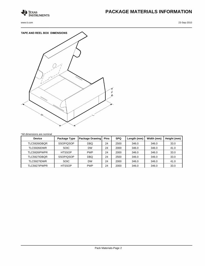
*All dimensions are nominal
Device Package Type Package Drawing Pins SPQ Length (mm) Width (mm) Height (mm)
TLC5926IDBQR SSOP/QSOP DBQ 24 2500 346.0 346.0 33.0
TLC5926IDWR SOIC DW 24 2000 346.0 346.0 41.0
TLC5926IPWPR HTSSOP PWP 24 2000 346.0 346.0 33.0
TLC5927IDBQR SSOP/QSOP DBQ 24 2500 346.0 346.0 33.0
TLC5927IDWR SOIC DW 24 2000 346.0 346.0 41.0
TLC5927IPWPR HTSSOP PWP 24 2000 346.0 346.0 33.0
PACKAGE MATERIALS INFORMATION
www.ti.com 23-Sep-2010
Pack Materials-Page 2

IMPORTANT NOTICE
Texas Instruments Incorporated and its subsidiaries (TI) reserve the right to make corrections, modifications, enhancements, improvements,and other changes to its products and services at any time and to discontinue any product or service without notice. Customers shouldobtain the latest relevant information before placing orders and should verify that such information is current and complete. All products aresold subject to TI’s terms and conditions of sale supplied at the time of order acknowledgment.
TI warrants performance of its hardware products to the specifications applicable at the time of sale in accordance with TI’s standardwarranty. Testing and other quality control techniques are used to the extent TI deems necessary to support this warranty. Except wheremandated by government requirements, testing of all parameters of each product is not necessarily performed.
TI assumes no liability for applications assistance or customer product design. Customers are responsible for their products andapplications using TI components. To minimize the risks associated with customer products and applications, customers should provideadequate design and operating safeguards.
TI does not warrant or represent that any license, either express or implied, is granted under any TI patent right, copyright, mask work right,or other TI intellectual property right relating to any combination, machine, or process in which TI products or services are used. Informationpublished by TI regarding third-party products or services does not constitute a license from TI to use such products or services or awarranty or endorsement thereof. Use of such information may require a license from a third party under the patents or other intellectualproperty of the third party, or a license from TI under the patents or other intellectual property of TI.
Reproduction of TI information in TI data books or data sheets is permissible only if reproduction is without alteration and is accompaniedby all associated warranties, conditions, limitations, and notices. Reproduction of this information with alteration is an unfair and deceptivebusiness practice. TI is not responsible or liable for such altered documentation. Information of third parties may be subject to additionalrestrictions.
Resale of TI products or services with statements different from or beyond the parameters stated by TI for that product or service voids allexpress and any implied warranties for the associated TI product or service and is an unfair and deceptive business practice. TI is notresponsible or liable for any such statements.
TI products are not authorized for use in safety-critical applications (such as life support) where a failure of the TI product would reasonablybe expected to cause severe personal injury or death, unless officers of the parties have executed an agreement specifically governingsuch use. Buyers represent that they have all necessary expertise in the safety and regulatory ramifications of their applications, andacknowledge and agree that they are solely responsible for all legal, regulatory and safety-related requirements concerning their productsand any use of TI products in such safety-critical applications, notwithstanding any applications-related information or support that may beprovided by TI. Further, Buyers must fully indemnify TI and its representatives against any damages arising out of the use of TI products insuch safety-critical applications.
TI products are neither designed nor intended for use in military/aerospace applications or environments unless the TI products arespecifically designated by TI as military-grade or "enhanced plastic." Only products designated by TI as military-grade meet militaryspecifications. Buyers acknowledge and agree that any such use of TI products which TI has not designated as military-grade is solely atthe Buyer's risk, and that they are solely responsible for compliance with all legal and regulatory requirements in connection with such use.
TI products are neither designed nor intended for use in automotive applications or environments unless the specific TI products aredesignated by TI as compliant with ISO/TS 16949 requirements. Buyers acknowledge and agree that, if they use any non-designatedproducts in automotive applications, TI will not be responsible for any failure to meet such requirements.
Following are URLs where you can obtain information on other Texas Instruments products and application solutions:
Products Applications
Audio www.ti.com/audio Communications and Telecom www.ti.com/communications
Amplifiers amplifier.ti.com Computers and Peripherals www.ti.com/computers
Data Converters dataconverter.ti.com Consumer Electronics www.ti.com/consumer-apps
DLP® Products www.dlp.com Energy and Lighting www.ti.com/energy
DSP dsp.ti.com Industrial www.ti.com/industrial
Clocks and Timers www.ti.com/clocks Medical www.ti.com/medical
Interface interface.ti.com Security www.ti.com/security
Logic logic.ti.com Space, Avionics and Defense www.ti.com/space-avionics-defense
Power Mgmt power.ti.com Transportation and Automotive www.ti.com/automotive
Microcontrollers microcontroller.ti.com Video and Imaging www.ti.com/video
RFID www.ti-rfid.com
OMAP Mobile Processors www.ti.com/omap
Wireless Connectivity www.ti.com/wirelessconnectivity
TI E2E Community Home Page e2e.ti.com
Mailing Address: Texas Instruments, Post Office Box 655303, Dallas, Texas 75265Copyright © 2011, Texas Instruments Incorporated