lead-free solder bump technologies for flip-chip packaging ... · lead-free solder bump...
TRANSCRIPT
Lead-Free Solder Bump Technologies for Flip-Chip Packaging Applications
Zaheed S. Karim1 and Jim Martin2 1Advanced Interconnect Technology Ltd.
1901 Sunley Centre, 9 Wing Yin Street, Tsuen Wan, Hong Kong Tel: (852) 2719-5440, Fax: (852) 2358-4766, E-mail: [email protected]
2Shipley LLC 455 Forest Street, Marlborough, MA 01752, USA
Tel: (516) 868-8800, Fax: (516) 868-4781, E-mail: [email protected]
Abstract
We describe the fabrication and characterization of five different types of lead-free solder bump interconnections for use in flip-chip electronic packaging applications. Lead-free solder bumps were fabricated from pure-tin (Sn), tin-bismuth (Sn:Bi), eutectic tin-copper (Sn:Cu), eutectic tin-silver (Sn:Ag), and ternary tin-silver-copper (Sn:Ag:Cu) alloys. The fabrication process consists of the electrolytic plating, using a fountain (cup) plater, of a 5 µm thick copper under-bump-metal (UBM) onto which is plated the lead-free solder. The as-plated bumps were subsequently re-flowed in a 5-zone re-flow oven. Due to the characteristic high-tin compositions of the lead-free solder alloys, which can cause the rapid and uneven formation of tin-copper intermetallics at the bump-UBM interface upon re-flow, a unique proprietary nickel “cap” using a single photolithography process that completely encapsulates the copper UBM was developed. Two different test structures, one with perimeter- and a second with area-distributed solder bumps, each with bumps of average size 125 µm diameter (post-re-flow) were fabricated onto “daisy-chain” wafers to characterize the lead-free solder bumping and bonding process and to conduct a series of reliability tests. Tests conducted to characterize the properties of the lead-free bumps included Scanning Electron Microscopy (SEM), Energy Dispersive X-ray (EDX), Auger Electron Spectroscopy (AES), micro-sectioning, and ball shear measurements for which the bumps were re-flowed multiple times and subjected to ball shear tests in-between re-flows to study the formation of intermetallic compounds. Lead-free solder bumped “daisy-chain” test die were also flip-chip bonded onto BT-epoxy substrates with patterned copper traces overplated with nickel/gold. The bonded die were underfilled and subjected to environmental tests consisting high-temperature storage, thermal cycling, and accelerated aging. Details of the lead-free solder bump fabrication process together with the performance results including their electrical, mechanical, and reliability characteristics will be presented for all five lead-free alloys chosen in this study.
Key words: lead-free, solder bumps, flip-chip, under-bump-metal Introduction
Restrictions on the use of lead-containing solders in electronic products are currently under consideration because it is believed that the lead from such products, which are typically disposed of in landfills, have the potential to leach out and contaminate the drinking water system. The electronics industry has been targeted to go “lead-free” despite the fact that less than 0.5% of all the lead produced annually in the world is used for electronic solders [1].
Laws banning the use of lead in electronics products are due to be enacted in the European Community in January 2008 and similar legislation to restrict the use of lead is pending in both the United States and in Japan [2]. Efforts to identify suitable lead-free finishes for electronic components has thus far been focused mainly on printed circuit boards, leadframe packages, and in the selection of solder pastes. Little attention has being paid to the fabrication of lead-free bump
interconnections which are required when packaging integrated circuits (ICs) by flip-chip bonding despite industry predictions that approximately 2.5% of all ICs manufactured in the year 2004 will have to be bumped and packaged using flip-chip [3]. Five different types of lead-free alloy bump materials, with tin constituting a major fraction of the solder, were selected as possible lead-free replacements on the basis of: i) worldwide resources and availability of tin; ii) the comparable cost of the lead-free alloys to lead-tin solder; iii) the bumps can be fabricated using conventional low-cost electroplating techniques; iv) the compatibility of tin-based solders with current re-flow processes, materials, and surface mount equipment, and; v) the familiarity of the electronics manufacturing and assembly industry in handling tin alloys. Tin-bismuth bumps with a composition of 90wt%Sn:10wt%Bi and a melting point (MP) of 200°C were fabricated as a potential replacement for eutectic lead-tin solder bumps which have a MP of 183°C. Lead-free bumps made of pure-tin with a MP of 232°C, eutectic tin-copper with a composition of 99.3wt%Sn:0.7wt%Cu with a MP of 227°C, and tin-silver with a eutectic composition of 96.5wt%Sn:3.5wt%Ag and a MP of 221°C were fabrcated as lead-free replacements for both eutectic and high melting point high-lead solder bumps. Ternary composition tin-silver-copper bumps with an alloy composition of 95.8wt%Sn:3.5wt%Ag:0.7wt%Cu and a MP of 216°C were also fabricated by electroplating using a unique process of sequential plating from two separate binary Sn:Cu and Sn:Ag plating solutions. Lead-Free Solder Bump Fabrication Process Lead-free bumps of average size 125 µm in diameter (post-re-flow) were plated onto silicon wafers patterned with perimeter- and area-distributed “daisy-chain” test structures (Figs. 1 and 2). Primary steps used in the fabrication of the lead-free bumps consisted of: a) A sputter cleaning step to remove the naturally
formed oxide layer on the aluminum bond pads followed by sputter deposition of chrome (thickness of 500 Å) and copper (thickness of 5,000 Å). These two sputtered metals effectively form the adhesion, barrier to indiffusion, and electrical buss layers for plating.
b) Patterning of the wafer with an 80 µm thick positive-tone liquid photoresist, positive chrome photomask, UV exposure (using a mask aligner), and developing the thick photoresist to define the areas to be plated.
c) Mounting of the wafer in a cup plater and application of current (using contacts at the edges of the wafer) to the underlying copper layer for plating of a 5 µm thick copper under-bump-metal (UBM) layer which acts as a "wettable" foundation to the lead-free solder bump upon re-flow.
d) Electroplating of lead-free solder bumps using the appropriate plating solution, anodes, and direct current (DC) or pulse-plating in a fountain (cup) plater system.
e) Removal of the thick photoresist and chemical etching of the sputtered copper and chrome layers.
f) Application of flux and re-flow of the as-plated bumps in a 5-zone re-flow oven to form the characteristic spherical solder bump shape.
Experimental Results
Difficulties encountered in the fabrication of the lead-free solder bumps consisted mainly in the control and measurement of the copper composition in the eutectic tin-copper plating bath and the plated deposit since the target value for the copper concentration was only 0.7%. Control of the copper concentration was achieved by continuosly adjusting and measuring the copper in the plating bath solution (provided by Shipley) and the plated deposit and by using pulse plating instead of direct current. Plating solutions were analysed for their copper content using Atomic Absorption Spectroscopy (AAS). Measurement of the composition in the plated deposit was achieved by using Auger Electron Spectroscopy (AES) on cross-sectioned re-flowed bumps. Additional techniques such as Differential Scanning Calorimetry (DSC) were also used to determine the melting point and the concentration of the copper in the bumps. Similar methods were used to control and measure the composition of the silver in the tin-silver plating bath (from Shipley) to achieve a eutectic tin-silver bump with approximately 3.5% silver. Accurate control of the percentage of the copper and silver in the eutectic tin-copper and tin-silver bumps is critical due to the rapid change in the melting point of alloys with only a small increase (~1%) in the composition of these two elements.
Examples of the as-plated and post re-flowed lead-free pure-tin, tin-bismuth, eutectic tin-copper, eutectic tin-silver, and tin-silver-copper bumps using the fabrication process steps described previously are shown in Scanning Electron Micrographs in Figs. 3-7 respectively. For the ternary tin-silver-copper bumps the fabrication process consisted of a unique method of sequentially plating tin-silver followed by tin-copper (Fig. 7a) and re-flowing the bump to completely mix
the solders. This was made possible in part due to the relatively close melting points of the tin-copper and tin-silver alloys.
Due to the higher melting point values for the lead-free pure-tin, tin-copper, tin-silver, and tin-silver-copper bumps, the peak re-flow temperatures used were between 250°C to 265°C.
During the fabrication and characterization of the lead-free solder bumps Scanning Electron Microscopy (SEM) and Scanning Auger Miroscopy (SAM) measurements on cross-sections of re-flowed tin-silver (3.5% silver) bumps indicated the rapid and uneven formation of tin-copper intermetallics at the interface between the copper UBM and the tin-rich lead-free solder bumps (Figs. 8a - 8d) [4]. This phenomenon was also observed in SAM analyses of the cross-sections of all the other lead-free solder bumps. In order to limit the excessive formation of the tin-copper intermetallic compound which is brittle and prone to failure particularly when the layer is too thick, a unique process which completely encapsulates the copper UBM using a single mask step was developed. SAM analysis on a nickel “capped” copper UBM indicates the effectiveness of this method (Figs. 9a – 9d). The advantage of using nickel is its relatively low dissolution rate in tin at 250°C compared to copper (~0.02 microinches per second for nickel compared to ~5.3 microinches per second for copper). All five lead-free solder bumps were subjected to ball shear tests after single and multiple re-flows (JESD22-B117). Preliminary results after single (1X) re-flow show average shear values in excess of 2.5 grams/mil2 (Table 1) for 100 µm diameter solder balls with all breakages occurring within the bulk of the solders and not at the solder to copper UBM interface. The sample size for the 1X re-flow test was 40 bumps for each solder type. Cross-sections of the bumps showed no detectable voids in the as-plated or post-re-flowed bumps and there was no formation of any tin-copper intermetallic due to the use of the nickel “cap”. Lead-free bumped perimeter and area-array daisy-chain test die were also flip-chip bonded onto BT-epoxy substrates, underfilled, and subjected to die shear and environmental tests to determine their suitability for flip-chip-on-board and flip-chip-in-package applications. Environmental tests consist of high-temperature storage (+150°C for 1,000 hours - JESD22-A103-A), thermal cycling (-40°C to +125°C for 1,000 cycles, 1 cycle/hour, 15 minutes dwell and 15 minutes ramp - JESD22-A104-A Level G), and accelerated aging (100% RH, 15 psig, +121°C for 96 hours - JESD22-A102-B Level C). Tests are on-going and results on the reliability studies will be presented at the conference.
Conclusions We have demonstrated the successful fabrication of five different types of lead-free solder bumps consisting of pure-tin, tin-bismuth, tin-copper, tin-silver, and tin-silver-copper. The method of fabrication for all lead-free alloys was by electroplating using a plated copper under-bump-metal. Results indicate that the application of a suitable barrier diffusion layer such as nickel is necessary to limit the excessive formation of tin-copper intermetallic compounds. Preliminary bump shear results have shown that all the lead-free bumps chosen in this study may be suitable replacements for eutectic and high-lead solders for use in various flip-chip electronic packaging applications. References [1] Ning-Cheng Lee, “Lead-Free Soldering – Where the World is Going”, Advancing Microelectronics, September/October 1999, pp. 29-35, 1999. [2] Greg Jones, “A Period of Adjustment: The Effect of Lead-Free Assembly on the Seminsiductor Iidustry”, Chip Scale Review, March/April 2000, pp. 48o TD 0 Tc -0.0529 29 Tc (-) 0 94.8 0 5 0.Scal316 Tw3plated copp35, 1999.
[2]-
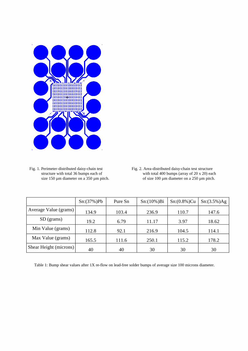
Fig. 1. Perimeter-distributed daisy-chain test Fig. 2. Area-distributed daisy-chain test structure structure with total 36 bumps each of with total 400 bumps (array of 20 x 20) each size 150 µm diameter on a 350 µm pitch. of size 100 µm diameter on a 250 µm pitch.
Sn:(37%)Pb Pure Sn Sn:(10%)Bi Sn:(0.8%)Cu Sn:(3.5%)Ag
Average Value (grams) 134.9 103.4 236.9 110.7 147.6 SD (grams) 19.2 6.79 11.17 3.97 18.62
Min Value (grams) 112.8 92.1 216.9 104.5 114.1 Max Value (grams) 165.5 111.6 250.1 115.2 178.2
Shear Height (microns) 40 40 30 30 30
Table 1: Bump shear values after 1X re-flow on lead-free solder bumps of average size 100 microns diameter.
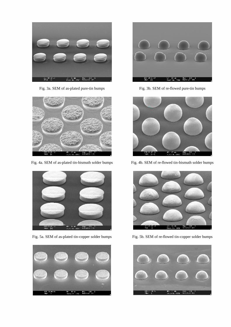
Fig. 3a. SEM of as-plated pure-tin bumps
Fig. 3b. SEM of re-flowed pure-tin bumps
Fig. 4a. SEM of as-plated tin-bismuth solder bumps
Fig. 4b. SEM of re-flowed tin-bismuth solder bumps
Fig. 5a. SEM of as-plated tin-copper solder bumps
Fig. 5b. SEM of re-flowed tin-copper solder bumps

Fig. 6a. SEM of as-plated tin-silver solder bumps
Fig. 6b. SEM of re-flowed tin-silver solder bumps
Fig. 7a. SEM of as-plated tin-silver-copper solder bumps (fabricated by sequential plating of tin-silver and tin-
copper)
Fig. 7b. SEM of re-flowed tin-silver-copper solder bumps
Fig. 8a. SEM of re-flowed cross-sectioned tin-silver bump at the interface between the copper UBM and
solder bump
Fig. 8b. SAM of re-flowed cross-sectioned tin-silver bump showing the distribution of copper at the interface
between the copper UBM and solder bump
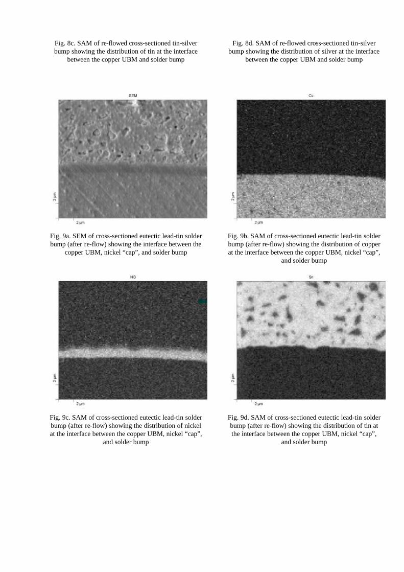
Fig. 8c. SAM of re-flowed cross-sectioned tin-silver bump showing the distribution of tin at the interface
between the copper UBM and solder bump
Fig. 8d. SAM of re-flowed cross-sectioned tin-silver bump showing the distribution of silver at the interface
between the copper UBM and solder bump
Fig. 9a. SEM of cross-sectioned eutectic lead-tin solder bump (after re-flow) showing the interface between the
copper UBM, nickel “cap”, and solder bump
Fig. 9b. SAM of cross-sectioned eutectic lead-tin solder bump (after re-flow) showing the distribution of copper at the interface between the copper UBM, nickel “cap”,
and solder bump
Fig. 9c. SAM of cross-sectioned eutectic lead-tin solder bump (after re-flow) showing the distribution of nickel at the interface between the copper UBM, nickel “cap”,
and solder bump
Fig. 9d. SAM of cross-sectioned eutectic lead-tin solder bump (after re-flow) showing the distribution of tin at the interface between the copper UBM, nickel “cap”,
and solder bump