solder joint reliability of flip chip bga...
TRANSCRIPT

SOLDER JOINT RELIABILITY OF
FLIP CHIP BGA PACKAGE
BY
LEE KOR OON
Thesis submitted in fulfillment of the
requirements for the degree of
Master of Science
March 2004

ii
ACKNOWLEDGEMENT
This work is funded by Intel Technology Sdn. Bhd. through a research grant. I’m very
grateful for Intel’s support in giving out the project.
I would like to express my deepest gratitude to Professor K. N. Seetharamu, my main
supervisor for his excellent guidance, support and counsel during the undertaking of this
work.
I would also like to express my sincere thanks to my co-supervisor, Dr. Ishak Hj. Abdul
Azid for his constant guidance, encouragement and support in helping me to finish the
project.
Special thanks go to my fellow friend, Ong Kang Eu for guiding me with ANSYSTM in
the initial stages of the work. Without his effort, this project would not have been
completed.
Last by not least, I dedicate this work to my parents, for bringing me to where I am
today.
THANK YOU!

iii
TABLE OF CONTENTS
ACKNOWLEDGEMENT ii
TABLE OF CONTENTS iii
LIST OF FIGURES vi
LIST OF TABLES viii
NOMENCLATURE x
ABSTRAK xii
ABSTRACT xiv
Chapter 1: Introduction
1.1 Flip Chip Technologies 1
1.2 Solder Joint Reliability 1
1.3 Finite Element Simulation 2
1.4 Artificial Neural Network (ANN) 3
1.5 Genetic Algorithm (GA) 4
1.6 Literature Survey 5
1.7 Objectives and Scope of Work 9
Chapter 2: Methodology
2.1 Solder-bumped Flip Chip Package 12
2.2 Solder Ball Fatigue Models 15
2.2.1 Simplified Flip Chip Model 17
2.2.2 Detailed Flip Chip Model 19

iv
2.3 Material Properties and Modified Anand Constants 21
2.3.1 Anand’s constitutive model and Darveaux’s constitutive model 23
2.4 Solder Joint Fatigue Life Prediction Methodology 27
2.5 Temperature Cycling Tests: B-Test and X-Test 29
2.6 ANSYSTM Solution Methodology 32
2.7 Summary 38
Chapter 3: Results and Discussion
3.1 Results 40
3.2 Simplified Flip Chip Model 42
3.2.1 B-Test 42
3.2.2 X-Test 43
3.2.3 Simulation Results 44
3.3 Detailed Flip Chip Model 46
3.3.1 B-Test 46
3.3.2 X-Test 47
3.3.3 Simulation Results 48
3.4 Discussion 50
Chapter 4: X-Test Parametric Study and Optimization
4.1 Parametric Study 52
4.2 Application of Artificial Neural Network for Fatigue Life Prediction 58
4.2.1 Prediction for the Parameter Board Thickness 60
4.2.2 Prediction for the Parameter Substrate Thickness 62
4.2.3 Prediction for the Parameter Bottom Die Size 64

v
4.2.4 Prediction for the Parameter Solder Ball Standoff Height 66
4.2.5 Prediction for the Parameter Solder Mask Opening 68
4.2.6 Prediction for the Parameter Bottom Die Thickness 70
4.2.7 Discussion 72
4.3 Verification of ANN Predictions 72
4.4 Parametric Optimization with ANN and GA 74
Chapter 5: Conclusion
5.1 Overall Conclusions 76
5.2 Suggestions for Future Work 77
BIBLIOGRAPHY 79
RECOMMENDED READING MATERIALS 82
APPENDIX A 83
APPENDIX B 90

vi
LIST OF FIGURES
Figure 1.1 Schematic of a solder flip chip interconnect system. 2
Figure 2.1 Package outline drawing. 12
Figure 2.2 Basic structure of a flip chip package. 13
Figure 2.3 Layer dimensions of package substrate. 13
Figure 2.4 Layer dimensions of printed circuit board. 13
Figure 2.5 Graphical details of the solder ball. 14
Figure 2.6 Boundary constraints applied to a typical slice model. 17
Figure 2.7 Simplified diagonal slice model of the flip chip package. 18
Figure 2.8 Meshed simplified slice model of the flip chip package. 18
Figure 2.9 Close-up details of a solder ball joint. 19
Figure 2.10 The resulting mesh of a solder ball joint. 19
Figure 2.11 Detailed diagonal slice model of the flip chip package. 20
Figure 2.12 Meshed detailed slice model of the flip chip package. 20
Figure 2.13 Close-up details of a solder ball joint for the detailed model. 21
Figure 2.14 The resulting mesh of a solder ball joint for the detailed model. 21
Figure 2.15 Temperature cycling test B. 31
Figure 2.16 Temperature cycling test X. 31
Figure 2.17 Solder joint fatigue life prediction method. 39
Figure 3.1 Simplified flip chip model:
B-test Von Mises stress distribution and plastic work. 42
Figure 3.2 Simplified flip chip model:
X-test Von Mises stress distribution and plastic work. 43

vii
Figure 3.3 Detailed flip chip model:
B-test Von-Mises stress distribution and plastic work. 46
Figure 3.4 Detailed flip chip model:
X-test Von-Mises stress distribution and plastic work. 47
Figure 4.1 Effect of board thickness on solder fatigue life. 55
Figure 4.2 Effect of substrate thickness on solder fatigue life. 55
Figure 4.3 Effect of bottom die size on solder fatigue life. 55
Figure 4.4 Effect of solder ball standoff height on solder fatigue life. 56
Figure 4.5 Effect of top solder mask opening on solder fatigue life. 56
Figure 4.6 Effect of bottom die thickness on solder fatigue life. 56
Figure 4.7 Effect of package dimensions on the solder fatigue life. 57
Figure 4.8 Effect of package dimensions on solder fatigue life. 58
Figure 4.9a ANN predictions for ball/substrate interface. 61
Figure 4.9b ANN predictions for ball/board interface. 61
Figure 4.10a ANN predictions for ball/substrate interface. 63
Figure 4.10b ANN predictions for ball/board interface. 63
Figure 4.11a ANN predictions for ball/substrate interface. 55
Figure 4.11b ANN predictions for ball/board interface. 65
Figure 4.12a ANN predictions for ball/substrate interface. 67
Figure 4.12b ANN predictions for ball/board interface. 67
Figure 4.13a ANN predictions for ball/substrate interface. 69
Figure 4.13b ANN predictions for ball/board interface. 69
Figure 4.14a ANN predictions for ball/substrate interface. 71
Figure 4.14b ANN predictions for ball/board interface. 71

viii
LIST OF TABLES
Table 2.1 Stack-up layer dimensions of the flip chip package. 14
Table 2.2 Die material properties. 21
Table 2.3 Die attach/underfill material properties. 22
Table 2.4 Mold material properties. 22
Table 2.5 Substrate material properties. 22
Table 2.6 Solder ball material properties. 22
Table 2.7 Printed circuit board material properties. 22
Table 2.8 Substrate mask/PCB mask material properties. 23
Table 2.9 Darveaux modified Anand constants. 26
Table 2.10 Darveaux K1 through K4 crack growth correlation constants. 28
Table 3.1 Detailed simulation results for simplified flip chip model. 45
Table 3.2 Detailed simulation results for detailed flip chip model. 49
Table 4.1 X-test parametric study. 54
Table 4.2 Data points for ANSYS and ANN. 59
Table 4.3 Data for ANSYS simulations and ANN predictions (board thickness). 60
Table 4.4 Data for ANSYS simulations and ANN predictions (substrate
thickness). 62
Table 4.5 Data for ANSYS simulations and ANN predictions (bottom die size). 64
Table 4.6 Data for ANSYS simulations and ANN predictions (solder ball height). 66
Table 4.7 Data for ANSYS simulations and ANN predictions (solder mask
opening). 68
Table 4.8 Data for ANSYS simulations and ANN predictions (bottom die size). 70
Table 4.9 Fatigue life comparison. 73

ix
Table 4.10 Parametric data for ball/substrate interface. 75

x
NOMENCLATURE
T Temperature
CTE Coefficient of thermal expansion
No Thermal cycles to crack initiation
ΔWave Change in plastic work
dNda Crack propagation rate per thermal cycle
αw The characteristic solder joint fatigue life
a Solder joint diameter
dtd pε Effective inelastic deformation rate
s Initial value of deformation resistance
Q/k Activation energy/Boltzmann’s constant
A Pre-exponential factor
ξ Multiplier of stress
m Strain rate sensitivity of stress
ho Hardening constant
s^ Coefficient for deformation resistance saturation value
n Strain rate sensitivity of saturation value
a’ Strain rate sensitivity of hardening
dtd sε Steady state strain rate
k Boltzmann’s constant
σ Applied stress
Qa Apparent activation energy

xi
n Stress exponent
α Stress level at which the power law dependence breaks down
εc Creep strain
εT Transient creep strain
B Transient creep coefficient
εp Time-independent plastic strain
G Shear modulus
Css, Cp, mp Constants
εin Total inelastic strain
Subscripts
ave average

xii
ABSTRAK
Daya tahan hubungan bebola pateri merupakan satu kriteria keboleharapan yang penting
dalam pempakejan elektronik moden. Untuk mengurangkan kos pembangunan dan
memaksimumkan performasi ketahanan pakej elektronik, analisis termaju menjadi satu
keperluan dalam fasa rekabentuk dan pembangunan pakej mikroelektronik. Simulasi
analitikal komputer seperti analisa unsur terhingga boleh memberi satu gambaran
terperinci tentang taburan dan sejarah tegangan/tegasan pateri di bawah pelbagai
bebanan yang berbeza. Ia juga merupakan satu alat pengoptimuman yang sesuai untuk
melakukan kajian parametrik.
Analisa unsur terhingga tiga dimensi digunakan untuk menentukan respon
kelesuan hubungan pateri suatu pakej di bawah keadaan perubahan suhu berulang-alik
terpecut. Oleh kerana terdapat perbezaan dalam kadar pengembangan haba bagi setiap
bahan yang digunakan untuk menghasilkan suatu pakej, perubahan suhu menyebabkan
ketidakseimbangan pengembangan pakej dan seterusnya menyebabkan tegasan
hubungan bebola pateri. Penghasilan tegasan tersebut yang berulang kali akhirnya
menyebabkan kegagalan hubungan pateri, suatu mekanisma yang biasanya dikenali
sebagai kelesuan berulang-alik rendah.
Struktur bebola pateri menampung kebanyakan daripada ketegangan plastik
yang dihasilkan semasa perubahan suhu berulang-alik terpecut. Oleh sebab ketegangan
plastik merupakan parameter dominan yang mempengaruhi kelesuan berulang-alik
rendah, ia digunakan sebagai asas evaluasi untuk menentukan keboleharapan struktur
bebola pateri. Satu kaedah peramalan jangka hayat bebola pateri yang telah diterbitkan
akan digunakan di mana hasil keputusan daripada simulasi kaedah unsur terhingga
diterjemah kepada ramalan jangka hayat untuk kegagalan. Kajian ini membincangkan

xiii
kaedah analisis seperti yang dilaksanakan dalam perisian komputer kaedah simulasi
unsur terhingga ANSYSTM dan juga keputusan jangka hayat bebola pateri pakej yang
dihasilkan. Rangkaian Neural Tiruan (ANN) akan digunakan untuk melengkapkan
kajian parameter dan seterusnya Algoritma Genetik (GA) akan digunakan untuk
menyiasat gabungan parameter-parameter yang diperlukan bagi suatu jangka hayat yang
tertentu.

xiv
ABSTRACT
The integrity of ball and bump solder joints is a major reliability concern in modern
micro electronic packages. To minimize development costs and maximize reliability
performance, advanced analysis is a necessity during the design and development phase
of a microelectronic package. Computer simulation such as finite element analysis can
provide a very detailed description of solder stress/strain distribution and history under a
variety of loading conditions, and it is a powerful tool for performing parametric studies
and design optimization.
Three-dimensional finite element analysis has been applied to determine the
time-dependent solder joint fatigue response of a package under accelerated temperature
cycling conditions. Due to the difference in the thermal expansion of the various
materials involved in the construction of a typical package, temperature variations
create a mismatch in package expansion which ultimately results in solder joint stress.
Repeated application of this stress eventually causes solder joint failure, a mechanism
commonly known as low cycle fatigue.
The solder structures accommodate the bulk of the plastic strain that is generated
during accelerated temperature cycle. Since plastic strain is a dominant parameter that
influences low-cycle fatigue, it is used as a basis for evaluation of solder joint structural
integrity. An extensively published and correlated solder joint fatigue life prediction
methodology was incorporated by which finite element simulation results were
translated into estimated cycles to failure. This study discusses the analysis
methodologies as implemented in the ANSYSTM finite element simulation software tool
and the corresponding results for the solder joint fatigue life. Artificial Neural Network
(ANN) has been used to consolidate the parametric studies and then the evaluation of

xv
parameters to give a particular fatigue life is achieved by the use of Genetic Algorithm
(GA).

1
CHAPTER 1
INTRODUCTION
1.1 Flip Chip Technologies
Flip chip technology, in the book edited by Lau (Lau, 1995) is defined as placing
a chip to the substrate by flipping over the chip so that the I/O area of the chip is facing
the substrate. By flipping over the chip, the interconnection between the chip and the
substrate are achieved by conductive “bumps” placed directly in between the die surface
and the substrate. Therefore, the whole chip surface can be utilized for active
interconnections and at the same time, eliminates the need for wire bonding.
An internet source, (FlipChips Dot Com, 2001) indicates that flip chip
interconnection has been introduced since the early sixties by IBM for use in their
mainframe computers and IBM has continued to use flip chip up to the present day. The
same source also acknowledges the role played by Delco Electronics in helping to
develop flip chip for automotive applications in the seventies. These early developments
together with the advantages of flip chip packaging technology which offers smaller
chip size, higher I/O density with area array, better electrical performance and lowest
cost interconnection for high volume automated production results in flip chip
packaging being considered as the preferred choice over other conventional wafer level
packaging technology (Meilhon et al., 2003).
1.2 Solder Joint Reliability
There are essentially three basic elements in the solder flip chip interconnect
systems (Fig. 1.1). These include the chip, the solder bump, and the substrate. The
solder bumps in a flip chip interconnect system has three functions. First, the solder

2
joint forms the electrical connection between the chip and the substrate. Second the
solder joint also serve as a path for heat dissipation from the chip.
Fig. 1.1 Schematic of a solder flip chip interconnect system (Pang, 2001a)
Lastly, the solder joint provides the structural link between the chip and the substrate.
The structural integrity of the solder joint affects both the electrical and thermal
performances of the flip chip interconnect system. Degradation in the structural integrity
can be a reliability concern.
Another reliability concern is the thermo-mechanical behaviour of the solder
joint. Thermal mismatch deformations due to the different coefficient of thermal
expansion (CTE) between different materials used in the package can cause mechanical
stresses in the solder joint. This will eventually cause crack growth and leads to failure
in the package.
1.3 Finite Element Simulation
The effect of temperature cycling on the reliability of microelectronic packages
has been the subject of many studies. Because of the difference in the thermal expansion
of the multiple materials involved in the construction of a typical package, temperature
variations create a mismatch ultimately resulting in solder joint stress. Repeated
application of this stress eventually causes solder joint failure, a mechanism commonly
known as low cycle fatigue.
Silicon DieSolder Joint
PCB
Encapsulant

3
To minimize development costs and maximize reliability performance, advanced
analysis is a necessity during the design and development phase of a microelectronic
package. Computer simulation such as finite element analysis can provide a very
detailed description of solder stress/strain distribution and history under a variety of
loading conditions, and is a powerful tool for performing parametric studies and design
optimization. However, analyst is typically interested in the cycles to failure that a
package design configuration and cyclic loading condition will cause. This requires the
utilization of a life prediction methodology in which data typically provided by a finite
element solution can be translated into cycles to solder joint failure.
1.4 Artificial Neural Network (ANN)
Artificial Neural Network is a system loosely modeled based on the human
brain. Among the names frequently encountered in the field are connectionism, parallel
distributed processing, neuro-computing, natural intelligent systems, machine learning
algorithms, and artificial neural networks (Klerfors, 1998).
An artificial neural network operates by establishing links between many
different processing elements, each akin to a single neuron in the natural brain. Each
neuron receives many input signals, then, based on an internal weighting system
produces a single output signal that’s usually sent as input to another neuron. The
neurons are closely interconnected and organized into different layers. The input layer
receives the input, the output layer produces the final output. Usually one or more
concealed layers are sandwiched in between the two. This configuration makes it
impossible to predict or know the exact flow of data.
ANNs normally begin with randomized weights for all their neurons. This
means that they don’t “know” anything and must be taught to solve the particular

4
problem for which they are intended. Generally speaking, there are many learning laws
by which ANN can learn, such as Hebb’s Rule, Hopfield Law, The Delta Rule, and
Kohenen’s Learning Law (Klerfors, 1998), depending on the problem it must solve. A
self-organizing ANN (often called a Kohonen after its inventor) is exposed to large
amounts of data and tends to discover patterns and relationships in that data.
Researchers often use this type to analyze experimental data. A back-propagation ANN,
conversely, is trained by humans to perform specific tasks. During the training period,
the user evaluates whether if the ANN’s output is accurate. If it’s accurate, the neural
weightings that produced that output are reinforced; if the output is incorrect, those
weightings responsible are diminished. This type is most often used for cognitive
research and for problem-solving applications.
1.5 Genetic Algorithm (GA)
Genetic Algorithm (GA) as described in the book by Goldberg (Goldberg, 1997)
is an adaptive search method based on Darwin’s principles of natural selection, survival
of the fittest and natural genetics. They combine survival of the fittest among string
structures with a well-organized random information exchange to form a search
algorithm very comparable to some of the innovative flair of human search. As in
human genetics, GA exploits the fittest traits of old individuals to create a new
generation of artificial creatures (strings). With each generation, a better population of
individuals is created to replace the old population. Based on these principles, genetic
algorithm is developed as a search tool that efficiently exploits historical information to
speculate on new search points with expected improved performance.
The genetic algorithm determines which individual should survive, which should
reproduce and which should die. It also records statistics and decides how long the

5
evolution should continue. In GA, a population of individuals (parents) within a
machine represented by chromosomes is generated. Each individual in the population
represents a possible solution to a given problem. The individuals in the population then
go through a process of evolution. This process of evolution involves each individual
being evaluated and given a fitness score according to how well it is suited to be a
solution to the problem. Individuals with a high fitness score will be selected and
allowed to reproduce with other individuals in the population. The properties of each
individual are described by using a chromosome and reproduction within individuals
occurs through the crossover and mutation process. These two processes produce new
individuals that will become the new population of solutions for the next generation.
Members of the population with a low fitness score will be discarded and are unlikely to
be selected for the next evolution process.
The entire process of evaluation and reproduction then continues until either the
population converges to an optimal solution for the problem or the genetic algorithm
has run for a specific number of generations.
With these capabilities, GA will be applied together with ANN as a tool for
search and optimization purposes.
1.6 Literature Survey
Advances in the electronic industry leave in its wake a trail of reliability
problems. The integrity of ball and bump solder joints is one of the major reliability
concerns in modern microelectronic packages. A wide variety of literature is scanned
for work done in addressing the reliability issues in microelectronic packages,
particularly on the solder joint interconnect system. The search results indicate that quite
a substantial amount of work has been done in this area since the last two decades.

6
In more recent years, many studies have been done on thermal stress/strain
analysis on microelectronic packages. Li et al. (2003) utilized digital image correlation
technique to obtain the deformation field of a Ball Grid Array (BGA) package. The
results enable the authors to determine the strain/shear stress distribution of the package
under thermal loading. More direct study on the solder joint itself has also been carried
out by means of experimental work and computer simulations. Finite element analysis
has in the past few years become a popular and powerful tool for researchers tackling
the reliability issue of microelectronic packages.
Beh et al. (2003) utilized commercial finite element analysis software,
ABAQUS to study the second level solder joint reliability risk of a Flip Chip Ball Grid
Array (FCBGA) in temperature cycling reliability test. The effects of different ball grid
array pattern and board thickness on the solder joint reliability of the FCBGA package
have also been investigated.
Tee et al. (2003a) studied the design optimization of wafer-level Chip Scale
Package (CSP) for improved solder joint reliability performance with fatigue modeling.
Here the authors utilized a fatigue model based on a modified Darveaux’s approach with
non-linear viscoplastic analysis of solder joints (Darveaux, 1997; Darveaux, 2000).
Design analysis is also performed on several critical design parameters.
Tee et al. (2003b) established a creep model for Thin-profile Fine-pitch Ball
Grid Array (TFBGA) on board by PAKSI, a customized solder joint fatigue modeling
software, to predict the fatigue life of solder joint during thermal cycling test. A
parametric study on the design analysis of TFBGA was also carried out.
Stoyanov et al. (2001) applied computational modeling for flip chip assemblies
where thermo-mechanical simulations were used together with numerical optimization
and approximation techniques. The authors detailed the modeling integration approach

7
taken between the computational mechanics code-PHYSICA, and design optimization
tool-VisualDOC.
Pang et al. (2001a) adopted a phenomenological approach in thermal analysis in
which time independent plasticity and time dependent creep deformations are modeled
separately. The phenomenological approach adopted by Pang describes the
selectiveness of implementation (hence phenomenological) of the time independent
plasticity and time dependent creep analysis in the author’s two methods of analysis
namely the dwell creep and full creep methods. Plasticity is defined by the propensity of
a material to undergo permanent deformation under load. Time dependent plasticity and
time independent plasticity indicates plasticity behaviour that either depends on time or
independent of time. The full creep analysis models creep deformations during the
temperature ramps as compared to the dwell creep analysis which omits creep behaviour
during temperature ramps. A comparison was made with a rate dependent viscoplastic
analysis approach. When creep is taken into consideration together with plasticity, then
the term viscoplastic is defined. Therefore a rate dependent viscoplastic analysis
indicates the analysis of time-dependent creep behaviour and time-dependent plastic
behaviour.
Pang et al. (2001b) investigates the effects of employing different two-
dimensional (2-D) and three-dimensional (3-D) finite element analysis (FEA) models
for analyzing the solder joint reliability performance of a flip chip on board assembly.
The FEA models investigated were the 2-D-plane strain, 2-D-plane stress, 3-D-1/8th
symmetry and 3-D-strip models. Results indicate that the 2-D-plane strain and 2-D-
plane stress model simulation have the highest and lowest strain in solder respectively.
The 3-D-1/8th symmetry model gave solder strain results closer to the 2-D-plane strain
8
model, while the 3-D-strip model results fall closer to the 2-D-plane stress model. The
3-D results are clearly bounded by the 2-D-plane strain and 2-D-plane stress results.
Chandran et al. (2000) studied the reliability of solder joints by observing BGA
fatigue failures on different test vehicles. Finite element analysis and physical failure
analysis were used to determine the risk to the product. A parametric finite element
analysis was also carried out to determine the effect of design features and package
BGA layout pattern on the propensity of fatigue failure.
Zahn (2000a) applied three-dimensional finite element analysis to determine the
time-dependent solder joint fatigue response of a tape based chip scale package under
accelerated temperature cycling conditions. The effects of differing ball via
configurations due to variations in both package assembly and tape vendors were also
investigated.
Zahn (2000b) utilized viscoplastic finite element simulatioin methodologies to
predict ball and bump solder joint reliability for a silicon based five-chip multi-chip
module package under accelerated temperature cycling conditions. The analysis utilized
the ANSYS sub-modeling methodology by which global model simulation results were
applied as boundary conditions in localized sub-models of the solder balls and bumps.
Zahn (2000c) studied the effect of multiple die attach material configurations on
the solder joint reliability for a same die size, stacked, chip scale, ball grid array
package under accelerated temperature cycling conditions by using viscoplastic finite-
element simulation methodologies.
Yao et al. (1999) developed two dimensional and three dimensional finite
element models to numerically predict the stress, total strain, plastic strain, and
cumulative plastic strain of the solder joints in an ATC 4.1 flip chip test vehicle, a
microBGA, and a Chip Scale Package under temperature cycling. These stress and

9
strain values have been used to predict the solder joint lifetime through either strain-
based approaches such as Coffin-Manson and modified Coffin-Manson equations, or
stress-based approach (S-N curve).
Many more studies have been done on the issue of solder joint reliability and
new findings are being constantly put forward for publications. It is clear that there are
many challenges yet to be solved on the solder joint reliability. As solder joint
interconnect remains the preferred choice for functionality and performance in today’s
microelectronic packages, many more work can be done to improve the reliability of
solder joints. In view of this, a study of the solder joint reliability of a typical flip chip
package will be carried out. It can be observed from the literature as well that some of
the work involves parametric study as well. However, there has been no researcher so
far that utilizes ANN and GA to consolidate his/her parametric analysis.
1.7 Objectives and Scope of Work
Many investigators have studied the low-cycle fatigue life of solder bumps
under accelerated thermal cycling test (e.g. Popelar et al. (2000), Darveaux (2000), Zahn
(2000a), Zahn (2000b), Wiese et al. (2001), Lau et al. (2002), Schubert et al. (2002),
Dutta et al. (2002), & Schubert et al. (2003). It is true that many package configurations
studied by these researchers roughly have the same build-up and each of the case studies
utilizes a fatigue life prediction methodology not much different from one another. Even
solder fatigue lives predicted fall within a certain common range of a few hundred
cycles to a few thousand cycles. However, despite all these work, not a single analysis
approach and results obtained for a case study can be directly used for another case
study. There will be too many irregularities that must be accounted for in order to
compare any two case studies. Hence, even if fatigue life prediction methodology using

10
plastic work is not new, different case study with different package configuration and
different thermal cycle profile warrants the need for a simulation to be carried out in
order to determine its solder fatigue life.
The objective of this work will be to predict the low-cycle fatigue life of a flip
chip package subjected to two different accelerated temperature cycling test conditions.
Temperature fluctuations caused by either power transients or environmental changes,
along with the resulting thermal expansion mismatch between the various package
materials, results in time and temperature dependent creep deformation of solder. This
deformation accumulates with repeated cycling and ultimately causes solder joint
cracking and interconnect failure. Due to the thermal mismatch in thermal expansion,
plastic strain is generated during temperature cycling and the solder structures
accommodate most of the plastic strain. Since plastic strain is a dominant parameter that
influences low-cycle fatigue, it will be used as a basis for evaluation of solder joint
structural integrity. An extensively published and correlated solder joint fatigue life
prediction methodology based on viscoplastic finite element simulation will be
incorporated by which finite element simulation results will be translated into estimated
cycles to failure. Due to availability, the program ANSYSTM will be used to run the
finite element simulations.
From the literature scan, many authors are also including package parametric
analysis or package design optimization as part of their solder joint reliability
investigations. However, most of the work on package parameter design analysis only
involves further simulation with different package configurations. Therefore, in addition
to the extra simulations, it is proposed that the Artificial Neural Network (ANN) be
used as a tool to predict other data points in the simulation results. This will reduce the
number of simulations required for parametric analysis.

11
ANN is a versatile prediction tool that can utilize existing simulation data for
training and in the process be able to establish a connection between the input used in
the training (package dimensions) and the output (solder joint fatigue life). By
establishing this connection, ANN can be used to predict the output for other inputs
other than those used in the training. ANN is also chosen because ANN does not depend
on any governing equations and is able to give predictions based on raw data alone. Due
to these reasons, ANN is a very suitable prediction tool to be utilized.
Parametric study in Chapter 4 is planned to be carried out by increasing or
decreasing chosen package dimensions to study their effects on the solder joint fatigue
life. In such scenario, the solder joint fatigue life can only be known after a simulation is
carried out or after a prediction is made. Once the effects of every package dimensions
on the solder fatigue life have been established, the solder fatigue life can be
appropriately adjusted to a higher fatigue life or a lower fatigue life by increasing or
decreasing a chosen package dimension. However, if the need arises that a certain solder
fatigue life value is to be the target, how would one know what combination of package
dimensions that can provide such a particular solder fatigue life? It is for this purpose
that Genetic Algorithm (GA) is proposed to be used. Without any governing equations,
and lacking the ability to work backwards from using the output (solder fatigue life) to
predict the input (package dimensions), many optimization techniques cannot be utilized
in such scenario. GA however can be linked up with ANN in order to make use of
ANN’s trained connection between the input and the output. By linking with ANN, GA
can randomly provide a determined range of inputs for ANN to predict the output. If the
output predicted is within the target output required, GA can easily store that set of
inputs and their corresponding output and move on to another looped search.

12
CHAPTER 2
METHODOLOGY
2.1 Solder-bumped Flip Chip Package
A typical flip chip package measuring 14×14mm, with 256 solder balls (16×16
full ball matrix), 0.80mm pitch and attached to a 50×50mm board is analyzed. There are
2 dies in the package. The top die measured 9×9mm and the bottom die measured
12×12mm. The package outline drawing is shown in Fig. 2.1.
Package cenneutral point.
tre
Fig. 2.1. Package outline drawing (Intel).
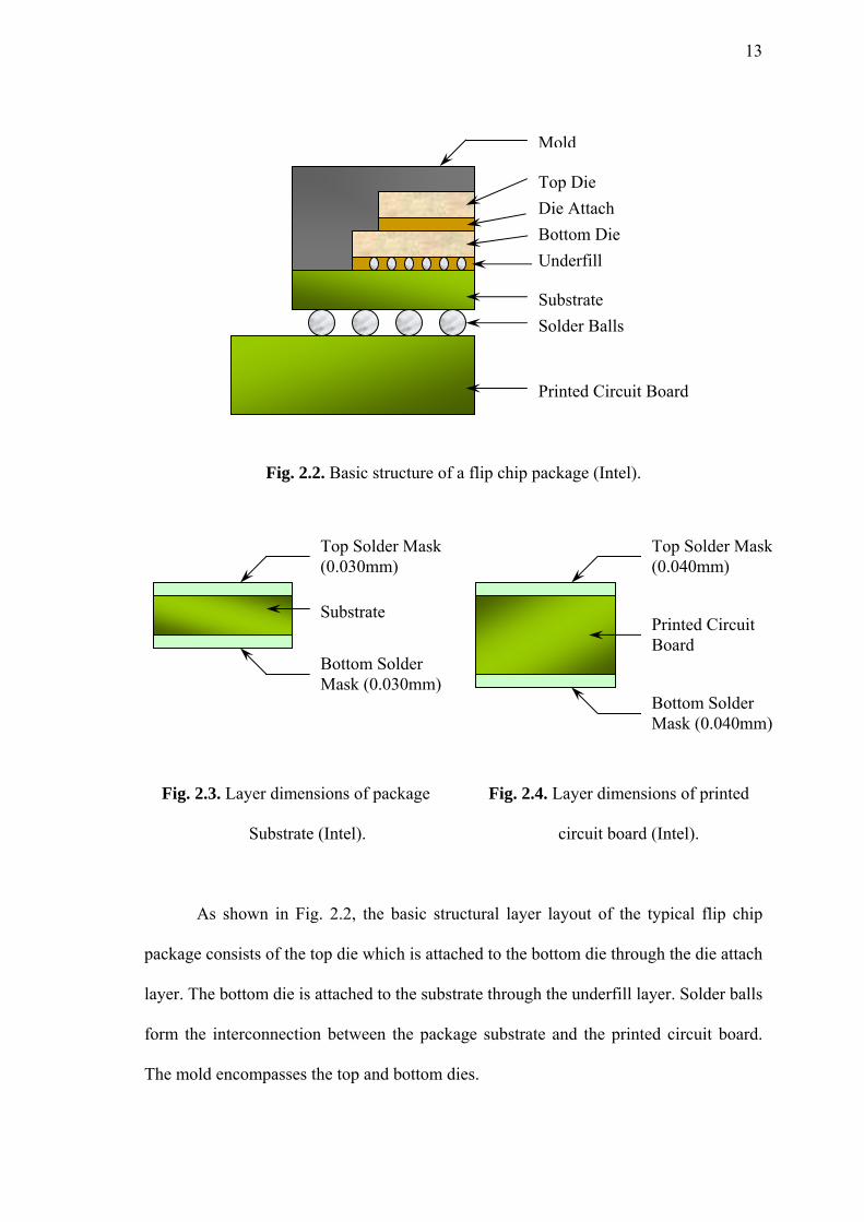
The basic structure of the solder-bumped flip chip package is shown in Fig. 2.2.
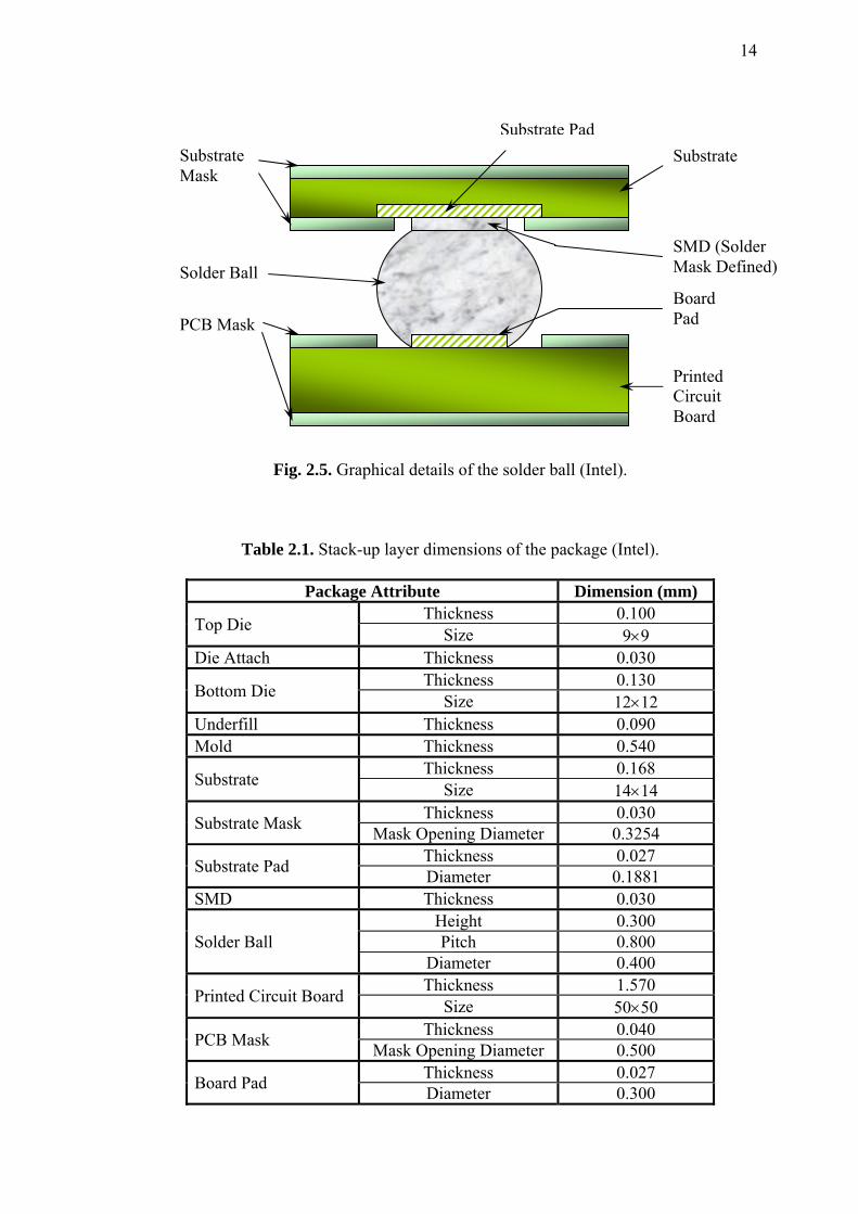
More detailed layer dimensions of the package substrate and printed circuit board are
shown in Figs. 2.3 and 2.4. Graphical details of the solder ball along with the package
substrate pad and the printed circuit board pad are shown in Fig. 2.5. The stack-up layer
dimensional information of the flip chip package is given in Table 2.1.
13
Mold
Top Die Die Attach Bottom Die Underfill
Substrate Solder Balls
Printed Circuit Board
Fig. 2.2. Basic structure of a flip chip package (Intel).
Top Solder Mask (0.030mm)
Top Solder Mask (0.040mm)
Substrate
Printed Circuit Board
Bottom Solder Mask (0.030mm)
Bottom Solder Mask (0.040mm)
Fig. 2.3. Layer dimensions of package Fig. 2.4. Layer dimensions of printed
Substrate (Intel). circuit board (Intel).
As shown in Fig. 2.2, the basic structural layer layout of the typical flip chip
package consists of the top die which is attached to the bottom die through the die attach
layer. The bottom die is attached to the substrate through the underfill layer. Solder balls
form the interconnection between the package substrate and the printed circuit board.
The mold encompasses the top and bottom dies.
14
Substrate Pad
Substrate Mask
Substrate
SMD (Solder Mask Defined)
Solder Ball Board Pad PCB Mask
Printed Circuit Board
Fig. 2.5. Graphical details of the solder ball (Intel).
Table 2.1. Stack-up layer dimensions of the package (Intel).
Package Attribute Dimension (mm)
Top Die Thickness 0.100 Size 9×9
Die Attach Thickness 0.030
Bottom Die Thickness 0.130 Size 12×12
Underfill Thickness 0.090 Mold Thickness 0.540
Substrate Thickness 0.168 Size 14×14
Substrate Mask Thickness 0.030 Mask Opening Diameter 0.3254
Substrate Pad Thickness 0.027 Diameter 0.1881
SMD Thickness 0.030
Solder Ball Height 0.300 Pitch 0.800
Diameter 0.400
Printed Circuit Board Thickness 1.570 Size 50×50
PCB Mask Thickness 0.040 Mask Opening Diameter 0.500
Board Pad Thickness 0.027 Diameter 0.300

15
Table 2.1 shows the dimensions of the typical flip chip package used in the
analysis. The top die has a thickness of 0.100 mm and the size of the die is 9×9 mm
square. Underneath the top die is the die attach with a layer thickness of 0.030 mm. The
top die and die attach is placed above the bottom die which has a thickness of 0.130 mm
with a die size of 12×12 mm square. Beneath the bottom die is a 0.090 mm thick layer
of underfill which connects the bottom die to the package substrate. The mold
encompasses the top and bottom dies as shown in Fig. 2.2 with a thickness of 0.540 mm
from the substrate. The package substrate surfaces have a 0.030 mm thick substrate
mask. Other details at the solder ball joint interfaces include a 0.027 mm thick substrate
pad with a diameter of 0.1881 mm and a 0.027 mm thick board pad with a diameter of
0.300 mm. The solder ball itself has a standoff height of 0.300 mm, a pitch of 0.800 mm
and a diameter of 0.400 mm. The printed circuit board is a 50×50 mm square board with
a thickness of 1.570 mm. The printed circuit board surfaces also have PCB masks of
0.040 mm thick.
2.2 Solder Ball Fatigue Models
Viscoplastic finite-element simulations methodologies are utilized to predict the
stress level and accumulated strain energy density per thermal cycle within the critical
solder ball of a package. Two models with different levels of package details are used
for the simulations. The first model is a simplified version of the flip chip package
where a few layer details are omitted from the simulation model. The second model is a
full model with more layer details incorporated into the simulation model. Omission of
a few layer details at the interface of the model is carried out in order to determine if
model simplification can produce results similar to a more complex model. For the
simplified model only the most necessary basic components of the package are drawn

16
and many small details at the solder ball interfaces are neglected, with a possible view
of obtaining results with much less effort. Due to the complex physics that encompass
this type of non-linear transient finite element analysis, only half of a diagonal slice of
the package was modeled in order to facilitate reasonable model run times. The
utilization of a half diagonal slice assures that a worst-case situation is simulated where
the perimeter solder ball is the farthest bump from the package centre neutral point
shown in Fig. 2.1. The half diagonal slice representing the finite element model is
shown by the diagonal bold print dashed line in Fig. 2.1.
The half diagonal slice model goes through the thickness of the overall package
assembly, taking into account all major components and a full set of halved solder joints.
Utilization of a slice model necessitates the consideration of boundary constraints that
has to be imposed on the slice model, which has to appropriately represent the actual
boundary conditions by which the full package assembly is subjected to. The
symmetrical diagonal plane remains planar and constant in the y-direction throughout
the analysis. The opposite side of the diagonal symmetric plane is neither a free surface
nor a true symmetry plane. A reasonable compromise is to couple the y-displacements
of the nodes on the slice plane. The effect of this constraint is that the slice plane is free
to move in the y-direction, but that the surface is required to remain planar. Boundary
constraints applied to a typical slice model are shown in Fig. 2.6. For all models
presented in this work, the printed circuit board length is truncated at a distance after the
package length. For a diagonal slice model, the ball pitch is the hypotenuse (1.1314mm)
of the true ball pitch (0.80mm). The y-dimension or width of the slice model is one-half
the solder ball pitch (0.5657mm).

17
UZ=0 on one node only
UY=0 on all plane surfaces
UX coupled on PCB vertical surface
UX=0 on all plane surfaces
UY coupled on all plane surfaces
Z
X Y
Fig. 2.6. Boundary constraints applied to a typical slice model (Zahn, 2000a).
2.2.1 Simplified Flip Chip Model
A simplified flip chip model is used for the first part of the simulation. The layer
configuration of the model is shown in Fig. 2.2. By comparing Fig. 2.2 with Figs. 2.3
through 2.5, a few details of the flip chip package assembly are omitted from this model.
The solder mask layers on the substrate and on the printed circuit board are not included
in this model. The substrate pads and the board pads are not included as well. The solder
mask defined (SMD) layer on top of the solder balls is also omitted from the model.
This configuration simplifies considerably the finite element model at the solder ball
joints and hence reduces the modeling and computational time required.
Based on Table 2.1, a three dimensional model of the flip chip package is drawn
using the commercial software ANSYSTM 7.0. The half diagonal slice finite element

18
model and the resulting mesh are shown in Figs. 2.7 and 2.8 respectively. The close-up
details at one of the solder ball joint and its resulting mesh are shown in Figs. 2.9 and
2.10 respectively.
Fig. 2.7. Simplified diagonal slice model of the flip chip package.
Fig. 2.8. Meshed simplified slice model of the flip chip package.

19
Fig. 2.9. Close-up details of a solder Fig. 2.10. The resulting mesh of a
ball joint. solder ball joint.
The entire model utilized a mapped or structured finite element mesh with 5506
elements and 7652 nodes. Typical solution run times are about 1.15 hours to 1.3 hours
depending on the accelerated temperature cycling test condition applied.
2.2.2 Detailed Flip Chip Model
For the second part of the simulation, a more detailed flip chip model is used for
simulation. As shown in Fig. 2.5, the SMD layer on top of each solder ball joints is
included in the model. The substrate pads and the board pads along with the solder mask
layers on the substrate and printed circuit board are included in the model. Based on
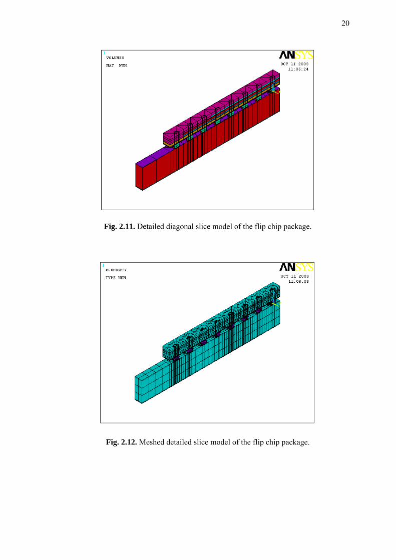
Table 2.1 and Figs. 2.2 through 2.5, a three dimensional model of the flip chip package
is drawn in ANSYSTM 7.0. The half diagonal slice finite element model and the
resulting mesh are shown in Figs. 2.11 and 2.12 respectively. The close-up details at one
of the solder ball joints and its resulting mesh are shown in Figs. 2.13 and 2.14
respectively
20
Fig. 2.11. Detailed diagonal slice model of the flip chip package.
Fig. 2.12. Meshed detailed slice model of the flip chip package.

21
Fig. 2.13. Close-up details of a solder Fig. 2.14. The resulting mesh of a solder
ball joint for the detailed model. ball joint for the detailed model.
The entire model utilized a mapped or structured finite element mesh with 6920
elements and 9308 nodes. Typical solution run times are about 1.25 hours to 1.42 hours
depending on the accelerated temperature cycling test condition applied.
2.3 Material Properties and Modified Anand Constants
Tables 2.2 through 2.8 show the material properties incorporated in the finite
element models. As seen from the tables, most of the properties used in the analysis are
dependent only on temperature.
Table 2.2. Die material properties (Intel).
Temp. (K) Young’s Modulus (MPa) Temp. (K) CTE (1/K) Poisson’s Ratio
213 131000 200 2.36E-6 0.279 233 131000 250 2.63E-6 273 130000 293 2.81E-6 293 130000 325 2.89E-6 323 130000 350 2.98E-6 373 129000 425 3.3E-6 500 129000 450 3.5E-6
500 3.61E-6

22
Table 2.3. Die attach/underfill material properties (Intel).
Young’s Modulus (MPa) CTE (1/K) Poisson’s Ratio -268349 + 4631.4T - 32.27T2
+ 0.117T3 - 0.0002T4
+ 2×10⁻⁷T5 - 1×10⁻¹⁰T6
-0.028 + 0.0005T - 4×10⁻⁶T2 + 1×10⁻⁸T3 - 3×10-11T4 + 3×10-14T5 – 1×10-17T6
0.3
Table 2.4. Mold material properties (Intel).
Temp. (K) Young’s Modulus (MPa) Temp. (K) CTE (1/K) Poisson’s Ratio
233 21300 223 1.545E-5 0.3 273 19900 410 5.020E-5 298 19000 435.5 3.901E-5 323 18100 573 4.192E-5 373 16100 423 2200 498 600
Table 2.5. Substrate material properties (Intel).
Young’s Modulus (MPa) Shear Modulus
(MPa) CTE (1/K) Poisson’s Ratio
29664 – 39.455T (X,Y) 1520 (X,Y) 1.6×10⁻⁵
(X,Y) 0.39 (X,Y,Z)
7800 (Z) 152 (Z) 6×10⁻⁵ (Z)
Table 2.6. Solder ball material properties (Intel).
Young’s Modulus (MPa) CTE (1/K) Poisson’s Ratio 75827 – 151.64T 2×10⁻⁵ + 2×10⁻⁸T 0.35
Table 2.7. Printed circuit board material properties (Intel).
Young’s Modulus (MPa) Shear Modulus
(MPa) CTE (1/K) Poisson’s Ratio
29664 – 39.455T (X,Y) 1520 (X,Y) 1.6×10⁻⁵
(X,Y) 0.39 (X,Y,Z)
7800 (Z) 152 (Z) 6×10⁻⁵ (Z)

23
Table 2.8. Substrate mask/PCB mask material properties (Intel).
Young’s Modulus (MPa) CTE (1/K) Poisson’s Ratio 4137 30×10-6 0.40
T is material properties temperature in Kelvin
2.3.1 Anand’s constitutive model and Darveaux’s constitutive model
Anand (1982) presented a constitutive model to describe the deformation of
metals at elevated temperature. Anand’s model is described by equations (1) to (4).
m
p
skTQA
dtd
1
sinhexp ⎥⎦
⎤⎢⎣
⎡⎟⎠⎞
⎜⎝⎛
⎟⎠⎞
⎜⎝⎛−=
σξε
(1)
( )dt
dBBBh
dtds pa
o
ε
⎥⎥⎦
⎤
⎢⎢⎣
⎡= ' (2)
*1ssB −= (3)
n
p
kTQ
Adtd
ss ⎥⎦
⎤⎢⎣
⎡⎟⎠⎞
⎜⎝⎛= exp
/^* ε
(4)
where dt
d pε is the effective inelastic deformation rate
s is the initial value of deformation resistance
Q/k is the activation energy/Boltzmann’s constant
A is the pre-exponential factor
ξ is the multiplier of stress
m is the strain rate sensitivity of stress
ho is the hardening constant
s^ is the coefficient for deformation resistance saturation value

24
n is the strain rate sensitivity of saturation value
a’ is the strain rate sensitivity of hardening
Anand’s constitutive relations are proposed for rate-dependent viscoplasticity
model. Plasticity is defined by the propensity of a material to undergo permanent
deformation under load. Viscoplasticity is defined when creep is taken into
consideration with plasticity. Anand’s model however does not consider rate-
independent plasticity.
Darveaux (2000) has through his work presented his constitutive relations that
describe the deformation behaviour of solder joints through equations (5) to (9) as
shown below. Steady state creep of solder is expressed by the relationship of
[ ] ⎟⎠⎞
⎜⎝⎛−=
kTQ
Cdt
d anss
s exp)sinh(ασε
(5)
where dt
d sε is the steady state strain rate, k is the Boltzmann’s constant, T is the absolute
temperature, σ is the applied stress, Qa is the apparent activation energy, n is the stress
exponent, α prescribes the stress level at which the power law dependence breaks down,
and Css is a constant.
Transient creep at constant stress and temperature can be described by
⎟⎟⎠
⎞⎜⎜⎝
⎛⎟⎠⎞
⎜⎝⎛−−+= t
dtd
Btdt
d sT
sc
εε
εε exp1 (6)

25
where εc is the creep strain, dt
d sε is the steady state creep rate, εT is the transient creep
strain, and B is the transient creep coefficient.
The instantaneous creep rate is given by
⎟⎟⎠
⎞⎜⎜⎝
⎛⎟⎠⎞
⎜⎝⎛−+= t
dtd
BBdt
ddt
d sT
sc εε
εεexp1 (7)
where dt
d sε is the steady state creep rate.
There is also a time-independent plastic strain component to the deformation at
high stresses when τ/G > 10-3.
pm
pp GC ⎟
⎠⎞
⎜⎝⎛=σε (8)
where εp is the time-independent plastic strain, G is the shear modulus, and Cp and mp
are constants. This component is not considered in Anand’s model. The total inelastic
strain is given by the sum of creep strain and plastic strain
εin = εc + εp (9)
where εin is the total inelastic strain.
As mentioned earlier, equation (8) is the time-independent plastic strain which
has not been taken into consideration by Anand’s model as Anand’s model is only
meant for a rate-dependent plasticity approach. Darveaux’s model however incorporates