keysight technologies achieving excellent spectrum...
TRANSCRIPT

Keysight Technologies Achieving Excellent Spectrum Analysis Results Using Innovative Noise, Image and Spur-Suppression Techniques
Application Note

2
Introduction
The need to measure spurious and harmonic signals is not new. However, emerging requirements include more of these measurements and specify demanding test conditions. In aerospace and defense applications, the task may be a search for known or unknown signals across a broad spec-trum. In wireless communications, the need is to characterize increasingly complex devices in an ever-increasing number of conditions and device states—and do so as quickly as pos-sible.
In all cases, searching for spurs and harmonics requires instrumentation that can help you find low-level signals at unknown frequencies across a wide frequency range. Making such measurements requires a spectrum or signal analyzer that can perform high-speed measurements with a low noise floor, minimal spurs and images, and high dynamic range.
As will be discussed here, signal analyzers generally fall into two broad categories: preselected and non-preselected. A typical preselected analyzer may not be fast enough for high-speed, high-resolution measurements. This is especially true of units that include a YIG-tuned preselection filter: sweeps generally take tens of milliseconds, which isn’t fast enough for many of today’s high-speed test requirements. By elimi-nating the preselection circuitry, non-preselected analyzers typically offer advantages in speed, accuracy and noise floor compared to preselected analyzers. However, unwanted images and spurious mixer products will significantly impair usability for general spectrum measurements.
The Keysight Technologies, Inc. M9393A PXIe performance vector signal analyzer (VSA) represents a breakthrough in the performance of non-preselected vector signal analyzers. In the modular form factor, Keysight has achieved high speed, a low noise floor and excellent dynamic range while dramati-cally reducing images and spurs. The underlying techniques include noise correction, image rejection and spur cancella-tion. This application note provides further explanation and elaboration of these techniques.
One note: As a simplification, the text will refer to the ana-lyzer as the M9393A. However, the functionality described here is provided by the interaction of the hardware within the M9393A, the spectrum analysis capability of the 89600 VSA software (89601B-200, -300 and -SSA options), and dedicated power spectrum functionality that manages fast averaging, image rejection (pages 6-7) and the “stepped FFT” process (page 7).
Building the foundationTwo key ideas provide a foundation for the techniques used in the M9393A: the power in combined signals and the basic math of noise correction. These are united in a third foun-dational element, which is a multi-step noise-correction process that is implemented inside the instrument. Let’s take a closer look at each of these topics.
Foundation 1: The power in combined signalsThe power of an RF signal is one of the few unambiguous definitions in electrical engineering: it is the average heating effect produced when a voltage is connected across a known resistance; the unit of measure is watts.
That’s fine for one signal. In the real world, signals combine through a variety of effects—intentional or otherwise—and we can see the results on the screen of a spectrum or signal analyzer. When two signals of equal power are added, several things may happen. If two identical signals are combined, the result has twice the amplitude and four times the power. If a signal is combined with its additive inverse, then they cancel each other and power will be at or near zero.
Venturing again into the real world, let’s suppose we have two totally uncorrelated noise-like signals of equal power. If we combine them, the result is one noisy signal with twice the power. Here’s why. The random noise predominantly present in electrical circuits is Gaussian: the mean is zero and the standard deviation is the RMS voltage. If we combine two uncorrelated, Gaussian signals, the probability distribution of the sum is the convolution of the individual probability distri-butions—and the result is another Gaussian distribution.
This new distribution has a variance that is the sum of the variances of the constituent Gaussian distributions. Be-cause variance is the square of the standard deviation, it has a direct relation to power. Thus, adding two uncorrelated Gaussian-noise signals creates another Gaussian-noise signal with a power that is the sum of the powers of the constituent signals. This result holds in general for any pair of uncorrelated signals.
Fundamentals Refresher: dBmPower levels in spectrum or signal analysis are rarely expressed in watts. Instead, we use “decibels refer-enced to 1 milliwatt,” which is abbreviated as dBm. The key equations are as follows:
– Power in dBm = 10*log (power in milliwatts) – Power in milliwatts = 10 (power in dBm/10)
As an example, 1 W of power equals 1000 mW and, from the above equation, that equals +30 dBm. Simi-larly, -60 dBm equals 10-6 mW or 1 nW. We’ll apply these relationships in the next two sections.
3
Foundation 2: The basics of noise correctionEvery instrument used to measure power has a noise floor. This is the power indicated on the display when the input signal is disconnected and terminated with a known load, typically 50 Ω.
Noise correction or “noise floor extension” (NFE) is an algo-rithm that improves measurement accuracy by using informa-tion about the instrument’s noise floor. For example, suppose the instrument reads –90 dBm when the input is discon-nected but reads –87 dBm when a signal from a test device is connected. What is the correct power value for the signal under test?
Hint: It isn’t –87 dBm. Here’s why. The initial noise-only measurement (N) of –90 dBm is 1 pW or 10-9 milliwatts. With a signal connected, the reading of –87 dBm is 2 pW or 2*10-9 milliwatts. Let’s express the addition of uncorrelated signals as follows: N is the original measurement and S+N is the sec-ond measurement. In this case, we know the following:
– N = 1 pW – (S+N) = 2 pW – S = (S + N) – N = 2 pW – 1 pW = 1 pW, = –90 dBm
Therefore, the signal power (S) is actually –90 dBm, not the indicated –87 dBm.
The noise correction algorithm of the M9393A goes through this process automatically: disconnects, moving the front-end switch way from the input; takes a measurement; connects, returning the front-end switch to the input; takes another measurement; and displays the corrected result on the analyzer screen.
As shown above, noise corrections can improve measurement accuracy. It can also extend dynamic range by 10 dB or more. To illustrate, suppose we connect another signal and the reading is –89 dBm:
– (S+N) = –89 dBm = 1.259 pW – N = –90 dBm = 1.000 pW – S = (S+N) – N = 1.259 – 1.000 = 0.259 pW = –95.87 dBm
In other words, the instrument accurately measured a signal that is almost 6 dB below the instrument’s noise floor. While this may seem impossible, it’s based on solid engineering principles.
As you might expect, the effectiveness of noise correction is directly affected by the accuracy and repeatability of the instrument itself. Noise correction neither magnifies nor reduces the basic error in the instrument’s measurements. While it can improve accuracy and sensitivity, it will increase the variability of a measurement, especially near the noise floor.
To illustrate this, let’s return to the first example: the in-strument reads –90 dBm with no signal present and –87 dBm with a signal connected. Assume the instrument has a repeatability of ±0.1 dB in this power range: (S+N) will vary from –87.1 dBm to –86.9 dBm; N will vary from –90.1 dBm to –89.9 dBm. Working in milliwatts yields the following ranges of values:
– (S+N) can vary from 1.950 pW to 2.042 pW – N can vary from 0.977 pW and 1.023 pW
From this, the calculated signal power [(S+N) – N] will vary as follows:
– 1.950 pW – 1.023 pW = 0.927 pW = –90.33 dBm – 2.042 pW – 0.977 pW = 1.065 pW = –89.73 dBm
Without noise correction, the result can vary by ±0.1 dB; however, the variation is approximately ±0.3 dB with noise correction. Thus, it is important to use averaging with noise correction to reduce the noise in a measurement.
Getting a good noise-corrected measurement also depends on a stable instrument setup—identical range, attenuation, gain, etc.—between the (S+N) and N measurements; the only difference should be the position of the front-end switch. Additionally, it’s best to make the two measurements—N and (S+N)—as close together in time as possible, thereby ensur-ing that there is little or no temperature change between measurements.
Within this process, it’s also important to switch the signal in and out as early as possible in the signal path—preferably at the input connector—to ensure that the N measurement includes noise from the entire instrument. It’s worth noting that measurement accuracy is slightly affected by switch-isolation specifications. When the switch is in the N position, some of the signal (S) present at the other input to the switch will leak through to the output. Fortunately, –30 dB of isola-tion is more than enough, and this is a reasonable value for an RF switch. Going through the noise-correction math, we can show the effect of this amount of isolation:
– (S+N) – (0.001*S + N) = 0.999*S – 10*log(0.999) = –0.00435 dB error
This small value is likely to be far below the calibration ac-curacy of the instrument.

4
Foundation 3: Our recipe for noise correctionBlending the preceding concepts into a step-by-step process yields a relatively simple recipe that is implemented by the M9393A. Here are the steps:
1. Take two measurements, one immediately after the other, that differ only in the state of a switch, which is as close to the input connecter as possible.
2. Perform the first measurement with the switch set such that the instrument sees the signal on the input connector for the (S+N) measurement. Perform the second measurement with the switch set such that the instrument sees a 50 Ω load for the N measurement.
3. Subtract the N value from the (S+N) value, producing a value for S.
4. If S is negative, negate it. In other words, we want S to be the absolute value of (S+N) – N or |(S+N) – N|, as power cannot be negative.
5. If S is zero or near zero, set it to epsilon to avoid taking the log of zero in step 6. We can choose epsilon to be 20 or 30 dB below the N measurement, which sets a new noise floor 20 to 30 dB below the original noise floor.
6. Convert S to dBm with the formula dBm = 10*log(S).
Step 4 requires further elaboration. During a measurement session, it’s possible that the input may be either unconnect-ed or have extremely low power at the measurement point. In such cases, with effectively no input signal, the instrument sees two independent measurements of its internal noise. Because either measurement could be larger than the other, taking the absolute value of the difference provides a correct result for all signal conditions.
Stepping backAs shown above, noise correction is based on foundational elements based on real science and good engineering. Standing on this solid ground, we can now explore further uses of this technique for residual reduction.
5
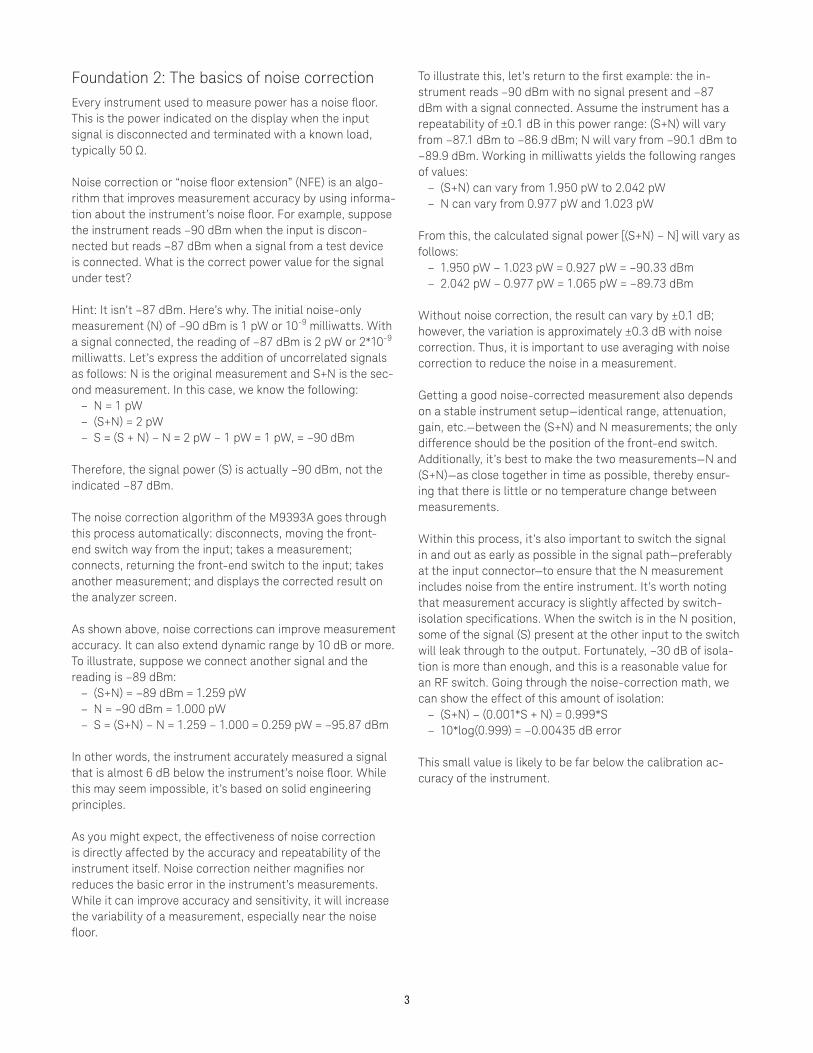
Using noise correction for residual reductionA spectrum analyzer display is simply a sequence of power measurements lined up along a range of individual frequen-cies. The bandwidth of each power measurement is set by adjusting the analyzer’s resolution bandwidth (RBW). Measurements are created by tuning or sweeping across the frequency range of interest, and this is (mostly) independent of the internal architecture of the analyzer: analog IF; digital IF; or sampling, digital filtering and the fast Fourier transform (FFT).
Two types of internally generated errors are especially troublesome in any signal analyzer: spurious responses and residual responses. Both are unwanted artifacts in a spec-trum display, and both represent errors in the measurement. For the sake of clarity, let’s be precise about the differences between the two. Residuals are unwanted responses that are unaffected by the presence of an input, meaning they are present with or without a signal at the input. In contrast, spurs are unwanted responses that show up only when an input is present. They scale along with the input’s amplitude, though not necessarily in a one-to-one relationship.
Figure 1. Noise correction provides a noticeable improvement in noise floor (right), but it can be disabled to further enhance measurement speed (left).
The noise-correction methodology described earlier can be used to significantly reduce residual responses in the M9393A signal chain. Because the residual responses remain the same in the S+N and N measurements, the noise-correc-tion algorithm will effectively subtract them out of the final result.
The inherent speed of the M9393A enables very fast mea-surements even with noise corrections activated. Even so, the noise-correction algorithm requires two measurements for every display trace and, to further increase speed, the M9393A gives you the option of disabling its noise-correction capability. This is useful when speed is of paramount im-portance and the noise floor of the instrument is unlikely to affect the measurement results. Thus, disabling noise correc-tion is a useful alternative in four situations: when the signals of interest are sufficiently above the noise floor, when your signal environment is relatively free of noise, when the noise isn’t significant enough to affect your measurements, or when you can live with the level of degradation that will be present in the results.

6
Exploring the basics of image rejection and spur cancellationThe M9393A provides another category of signal processing that allows for the suppression of the images and spurs that would normally be present in a non-preselected receiver. The basic architecture is superheterodyne, meaning the input (after scaling) is presented to the RF port of a mixer; the local oscillator (LO) port of the mixer is swept or stepped; and the IF port of the mixer is connected to a fixed-frequency detec-tion circuit in which filters are used to set the measurement bandwidth. In comparison, an instrument with a non-prese-lected front-end responds equally to RF inputs above and below the LO frequency.
Figure 3 shows a simplified block diagram of a traditional spectrum analyzer. Assume the IF circuitry is designed to respond to 300 MHz and we want to make a measurement between 3 and 4 GHz. In this case, the LO is swept from 2.7 GHz to 3.7 GHz and power is plotted on the display. If the input RF frequency is at 3.2 GHz, a response appears in the IF when the LO sweep reaches 2.9 GHz: fIF = 300 MHz = fRF – fLO. All is well until the LO reaches 3.5 GHz because another response is produced at the IF: -300 MHz = 3.2 GHz – 3.5 GHz. This “image” response is displayed at 3.8 GHz and has the same magnitude as the desired, correct response dis-played at 3.2 GHz.
Figure 3. This simplified block diagram shows the key elements inside a superheterodyne spectrum analyzer.
Fundamentals Refresher: MixingThe basics of mixing, as implemented inside a superhetero-dyne receiver, provide one more foundational element for this discussion. When the input RF signal is mixed with a stepped or sweeping LO, two IF signals are produced (Figure 2). One is the difference frequency at fIF = fRF – fLO and the other is the sum at fIF = fRF + fLO. In downconversion, the difference is always used to obtain a response within the bandwidth of the analyzer.
Figure 2. Mixing in a superheterodyne receiver produces two IF signals.
RF IF
F LO
F RFF LOF RF -F LO F RF +F LO
Input signal
LO
Signal
Swept frequency generator
Bandpass filter
Display
Mixer
IFRF
While this will always occur with a non-preselected front-end, there is a solution. We can identify the real and image components by performing two measurements and then applying some math operations to produce a single, correct result.
The measurements proceed as follows. As described above, the LO is swept from 2.7 to 3.7 GHz; we call this the low-side mix because the LO is lower than the input signal for a cor-rect response. The complementary measurement is created by sweeping from 3.3 GHz to 4.3 GHz—an offset of twice the IF from the other sweep—and we call this the high-side mix because the LO is higher than the input for a correct re-sponse (Figure 4).
Figure 4. In the superheterodyne spectrum analyzer, the low- and high-side mixing processes create two distinct responses.
300 MHzF2-F1
LO@ 3.5GHzF2
High-side mixing
RF inputSignal@ 3.2GHz
F1
300 MHzF1-F2
LO@ 2.9GHzF2
Low-side mixing
Pow
er (d
Bm
)Po
wer
(dB
m)
Pow
er (d
Bm
)
Frequency (Hz)
Frequency (Hz)
Frequency (Hz)

7
Superimposing the measurements atop one another, the low-side measurement will show responses at 3.2 GHz and 3.8 GHz on the display. The high-side mix will show a response at only 3.2 GHz. Where the two mixes agree (3.2 GHz), the response is real; where they disagree (3.8 GHz), the response is an image and can be rejected. This rejection can be done by simply combining the two constituent high-side and low-side results into a single display result through a “minimum” operator.
As a second example, we’ll change the input RF signal to 3.7 GHz. The low-side measurement will produce a single response at 3.7 GHz while the high-side mix will produce responses at 3.1 GHz (LO = 3.4 GHz) and 3.7 GHz (LO = 4.0 GHz). The common responses at 3.7 GHz agree and the single response at 3.1 GHz is an image that can be discarded.
This combination of low- and high-side mixes is also effective at dealing with internally generated spurious signals. While there are many sources of spurs, one of the most common is low-level modulation on the LO. If the LO has a small sinusoid located 1 MHz away, the front-end mixer will produce two outputs: the input signal translated down by the LO frequen-cy and a smaller, undesired copy of the input 1 MHz away.
Normally, LO-generated spurs are dependent on the LO frequency and will vary as the LO frequency changes. As a result, the unwanted spurious artifacts will appear at differ-ent places in the low- and high-side mixes and can thus be rejected, as is done with image responses.
Measuring with stepped FFTsBefore further detailing the operation of the “rejection” algorithm, it will be useful to describe the mechanism that is used to emulate sweeping in the M9393A. Rather than the continuous sweeping of a traditional spectrum ana-lyzer, the M9393A measures across wide frequency spans by concatenating a stepped series of FFTs. There is an LO; however, rather than sweeping, it steps across the specified range, pausing long enough at each step to acquire a block of time samples that is then transformed into the frequency domain with an FFT operation. After the block of time data is acquired, the LO takes a step less than or equal to the bandwidth just processed, gathers another block of samples and computes the next FFT. This process repeats until it reaches the end of the measurement span. The collection of stepped-FFT results comprises the equivalent of a swept measurement.
The frequency span that can be analyzed at each step is defined by the sample rate. Nyquist theory dictates that the complex sample rate must be greater than the signal band-width. In the M9393A, the maximum complex sample rate is
200 MHz. To account for filter-transition regions, the band-width is limited to 80 percent of the complex sample rate and therefore the usable frequency span is 160 MHz.
The size and resolution of each stepped FFT is a function of a few basics: the sample rate; the number of samples in the time block and the associated resolution in the frequency domain; the shape and selectivity of the chosen window function; the desired frequency span; and the specified RBW. These settings also affect what must be done at the concatenation points where successive stepped-FFT results are joined; one example is the use of overlap processing to compensate for time-domain windowing effects. Taken together, these are non-trivial computations that can put a heavy burden on the signal-processing hardware inside any signal analyzer.
Building on our previous discussion, stepped FFTs can be used with low- and high-side mixes inside the non-prese-lected analyzer. One key point is worth noting: the respective frequency axes for low- and high-side mixes are reversed (Figure 5). In the low-side mix, the frequency axis behaves as expected: if the input signal moves higher in frequency, the IF also moves higher and the responses are correctly ordered. The opposite occurs in the high-side mix: if the input signal moves up in frequency, it moves closer to the LO and therefore downward in frequency at the IF port. In this case the output of the FFT will be frequency-reversed—unless the hardware processor automatically compensates for the dif-ferences.
Figure 5. In the high-side case (lower right), the spectrum associated with FLO-FRF is reversed with respect to the input signal.
F LOF RF -F LO F RF +F LO
LO
RF IF
F LO
Input signal
FRF
F LOF LO -F RF F LO +F RF
Output from mixer for low-side mixing (F RF > F LO )
Output from mixer for high-side mixing (FRF < F LO )
Reversed

8
Sketching the algorithmTo accomplish image rejection, the M9393A takes two mea-surements, one with low-side mixing and the other with high-side mixing. Internally, it uses two power-versus-frequency arrays to produce a single, correct power-versus-frequency display.
This single result is created as the minimum of the two mea-surement arrays using the minimum value at each index point (i.e., frequency bin). Any response that appears in both arrays is correct and is retained. Because both show the same value (or nearly so), keeping the minimum provides a correct result. Any response that appears in only one of the arrays is false and can be rejected. In this case, taking the minimum provides a correct result because it ignores the larger false response (Figure 6).
Figure 6. The three traces shown here are a low-side measurement (top), a high-side measurement (middle) and the resulting spectrum that contains only real responses (bottom).
Figure 7. This simple functional diagram illustrates the operation of max/min hold for combining low- and high-side mixes.
Accounting for moving or pulsed signalsThe process described above usually works exceptionally well with frequency-stationary signals. Difficulties can arise with dynamic signals such as those that, from measurement to measurement, change in frequency or turn on and off. Un-aided, the normal operation of the algorithm described above will cancel all or part of the actual signal.
Measuring non-stationary signals is difficult with any type of analyzer, preselected or not. A variety of approaches make it possible to achieve accurate results.
One solution is a common feature of nearly all signal analyz-ers: the “max hold” display function. This accumulates, over time, the range of frequencies and amplitudes occupied by recurring, dynamic signals within the span of interest. There is a downside: getting a complete measurement takes time, and it is often ineffective with one-time, intermittent or spo-radic signals.
In a non-preselected analyzer that uses the image-cancelling algorithm outlined above, the problem is compounded by the interaction of the low- and high-side mixes. With dynamic signals, the two mixes are very likely to produce different re-sults, and this leads to rejection of real responses in the final measurement display. We can minimize this problem by mak-ing the low- and high-side measurements as close together in time as possible; however, even then, if the signal dynamics are fast enough, the real signals with self-cancel.
The solution is similar to the max-hold capability used in other analyzers—with one important difference. If the max-hold comparison is applied to the final image-rejection result, there will be little or no response to display. Until now, this has been a major limitation of image-rejection schemes—to the extent that it may have inhibited broader use of these techniques.
As implemented in the M9393A, the max-hold mechanism is applied separately to the low- and high-side mixes. With this approach, the minimum of the two max-hold results is dis-played (Figure 7): responses that coincide are retained; those that differ are rejected (Figure 8).
While this is an elegantly simple algorithm, it isn’t foolproof. The following discussions explore potential issues and the unique, innovative solutions that make the algorithm more robust.
Image rejected response
Min hold
Max hold
Max hold
Low-sideresponse
High-sideresponse

9
Figure 8. From top to bottom, these traces show the standard max-hold result (incorrect- image present), max hold from the low-side measure-ment (image present), max hold from the high-side measurement, and the ultimate correct result after image rejection and max/min hold.
Addressing pitfalls and enhancing robustnessAny image-rejection algorithm can be fooled into producing responses that aren’t real or potentially affect the real signal. In the M9393A, a truly innovative combination of technology and methodology has been used to make it more robust.
In a controlled lab environment, a typical algorithm will appear to work so well that it’s tempting to assume it will always produce a correct result. Of course, this is not so and we can demonstrate by constructing a pathological signal environment. After illustrating a problem scenario, we’ll de-scribe solutions that have been implemented in the M9393A.
Creating a pair of false resultsAssume the signal analyzer uses a complex sample rate of 200 MHz, which results in a measurement span, per FFT, of 160 MHz (80 percent of the sample rate). As used earlier, the IF is 300 MHz.
In this scenario, we want to measure a single FFT span cen-tered at 4 GHz. The displayed measurement will span from 3.92 GHz to 4.08 GHz (160 MHz centered on 4 GHz). For the low- and high-side measurements, the LO will be set to 3.7 GHz or 4.3 GHz, respectively (4 GHz ± 300 MHz).
For the sake of simplicity, the contrived environment contains just two frequency-stationary input signals, among which there is no component within the measurement range of 3.92 GHz to 4.08 GHz. Thus, any response that appears in the display will be erroneous.
10
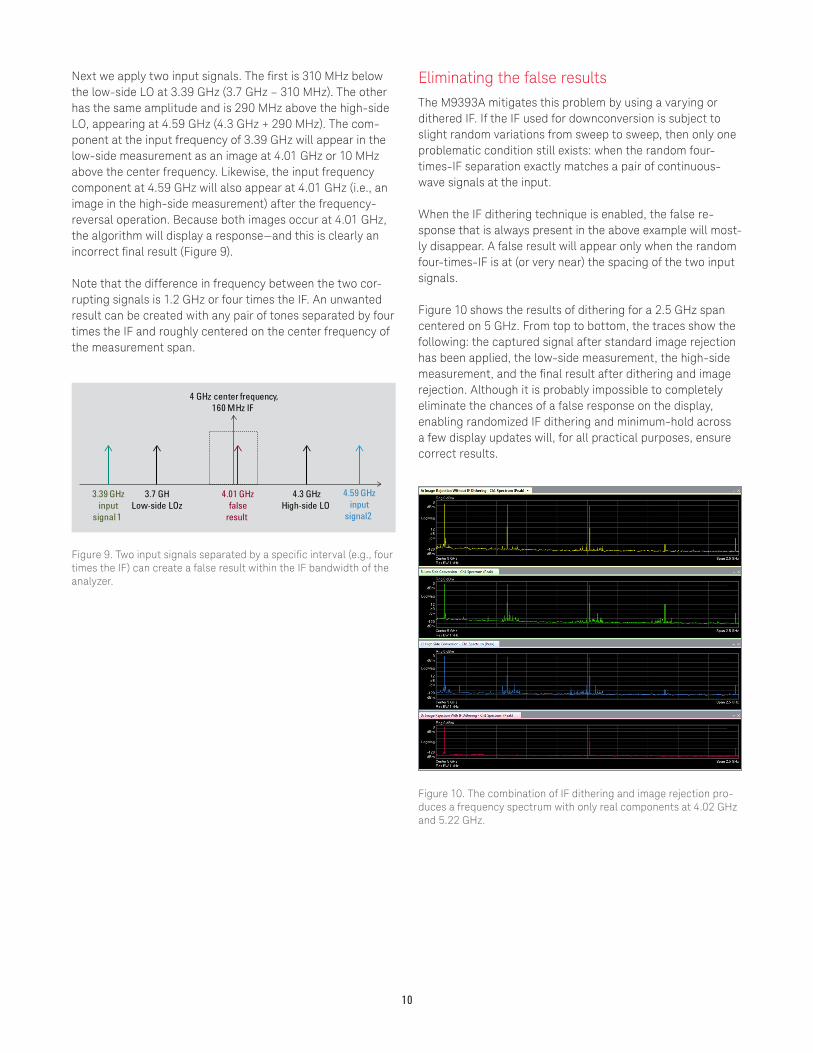
Next we apply two input signals. The first is 310 MHz below the low-side LO at 3.39 GHz (3.7 GHz – 310 MHz). The other has the same amplitude and is 290 MHz above the high-side LO, appearing at 4.59 GHz (4.3 GHz + 290 MHz). The com-ponent at the input frequency of 3.39 GHz will appear in the low-side measurement as an image at 4.01 GHz or 10 MHz above the center frequency. Likewise, the input frequency component at 4.59 GHz will also appear at 4.01 GHz (i.e., an image in the high-side measurement) after the frequency-reversal operation. Because both images occur at 4.01 GHz, the algorithm will display a response—and this is clearly an incorrect final result (Figure 9).
Note that the difference in frequency between the two cor-rupting signals is 1.2 GHz or four times the IF. An unwanted result can be created with any pair of tones separated by four times the IF and roughly centered on the center frequency of the measurement span.
Eliminating the false resultsThe M9393A mitigates this problem by using a varying or dithered IF. If the IF used for downconversion is subject to slight random variations from sweep to sweep, then only one problematic condition still exists: when the random four-times-IF separation exactly matches a pair of continuous-wave signals at the input.
When the IF dithering technique is enabled, the false re-sponse that is always present in the above example will most-ly disappear. A false result will appear only when the random four-times-IF is at (or very near) the spacing of the two input signals.
Figure 10 shows the results of dithering for a 2.5 GHz span centered on 5 GHz. From top to bottom, the traces show the following: the captured signal after standard image rejection has been applied, the low-side measurement, the high-side measurement, and the final result after dithering and image rejection. Although it is probably impossible to completely eliminate the chances of a false response on the display, enabling randomized IF dithering and minimum-hold across a few display updates will, for all practical purposes, ensure correct results.
Figure 9. Two input signals separated by a specific interval (e.g., four times the IF) can create a false result within the IF bandwidth of the analyzer.
4 GHz center frequency,160 MHz IF
3.7 GHLow-side LOz
4.3 GHzHigh-side LO
3.39 GHzinput
signal 1
4.59 GHzinput
signal2
4.01 GHzfalse
result
Figure 10. The combination of IF dithering and image rejection pro-duces a frequency spectrum with only real components at 4.02 GHz and 5.22 GHz.

11
ConclusionThe breakthroughs implemented in the M9393A PXIe perfor-mance VSA address four crucial problems: noise correction, residual reduction, image rejection and spur cancellation. These advances are derived from four main sources: algo-rithms, processing power, LO tuning speed, and the inherent speed of the PXI backplane.
The result is a signal analyzer that provides advantages to those who need to quickly locate known or unknown sig-nals—including spurs and harmonics—across a wide fre-quency range. The underlying algorithms also ensure greater confidence in the results presented on the display trace. These benefits are useful in a variety of applications: wireless communications, aerospace, defense, and more.
In the context of Keysight’s history of innovation, the M9393A is the realization of our microwave measurement expertise in modular form. It integrates core signal-analysis capabilities with hardware speed and accuracy, enabling you to tailor a solution to fit specific needs—today and tomorrow.
To discuss your requirements, please contact your local Key-sight sales representative or application specialist.
Webwww.keysight.com/find/M9393Awww.keysight.com/find/M9393AVSAwww.keysight.com/find/pxi
Related literature – Keysight M9393A PXIe performance VSA, Product Fact Sheet,
Literature part number 5991-4039EN

12 | Keysight | Achieving Excellent Spectrum Analysis Results Using Innovative Noise, Image and Spur-Suppression Techniques - Application Note
This information is subject to change without notice.© Keysight Technologies 2017Published in USA, December 1, 20175991-4039EN www.keysight.com
www.keysight.com/find/modularwww.keysight.com/find/M9393A
For more information on Keysight Technologies’ products, applications or services, please contact your local Keysight office. The complete list is available at:www.keysight.com/find/contactus
Americas Canada (877) 894 4414Brazil 55 11 3351 7010Mexico 001 800 254 2440United States (800) 829 4444
Asia PacificAustralia 1 800 629 485China 800 810 0189Hong Kong 800 938 693India 1 800 11 2626Japan 0120 (421) 345Korea 080 769 0800Malaysia 1 800 888 848Singapore 1 800 375 8100Taiwan 0800 047 866Other AP Countries (65) 6375 8100
Europe & Middle EastAustria 0800 001122Belgium 0800 58580Finland 0800 523252France 0805 980333Germany 0800 6270999Ireland 1800 832700Israel 1 809 343051Italy 800 599100Luxembourg +32 800 58580Netherlands 0800 0233200Russia 8800 5009286Spain 800 000154Sweden 0200 882255Switzerland 0800 805353
Opt. 1 (DE)Opt. 2 (FR)Opt. 3 (IT)
United Kingdom 0800 0260637
For other unlisted countries:www.keysight.com/find/contactus(BP-9-7-17)
DEKRA CertifiedISO9001 Quality Management System
www.keysight.com/go/qualityKeysight Technologies, Inc.DEKRA Certified ISO 9001:2015Quality Management System
Evolving Since 1939Our unique combination of hardware, software, services, and people can help you reach your next breakthrough. We are unlocking the future of technology. From Hewlett-Packard to Agilent to Keysight.
myKeysightwww.keysight.com/find/mykeysightA personalized view into the information most relevant to you.
www.keysight.com/find/emt_product_registrationRegister your products to get up-to-date product information and find warranty information.
Keysight Serviceswww.keysight.com/find/serviceKeysight Services can help from acquisition to renewal across your instrument’s lifecycle. Our comprehensive service offerings—one-stop calibration, repair, asset management, technology refresh, consulting, training and more—helps you improve product quality and lower costs.
Keysight Assurance Planswww.keysight.com/find/AssurancePlansUp to ten years of protection and no budgetary surprises to ensure your instruments are operating to specification, so you can rely on accurate measurements.
Keysight Channel Partnerswww.keysight.com/find/channelpartnersGet the best of both worlds: Keysight’s measurement expertise and product breadth, combined with channel partner convenience.