ka-band 2d luneburg lens design with glide-symmetric ...1142083/fulltext01.pdf · ka-band 2d...
TRANSCRIPT

IN DEGREE PROJECT ELECTRICAL ENGINEERING,SECOND CYCLE, 30 CREDITS
, STOCKHOLM SWEDEN 2017
Ka-band 2D Luneburg Lens Design with Glide-symmetric Metasurface
JINGWEI MIAO
KTH ROYAL INSTITUTE OF TECHNOLOGYSCHOOL OF ELECTRICAL ENGINEERING

TRITA 2017:115
ISSN 1653-5146
www.kth.se

Ka-band 2D Luneburg Lens Design
with Glide-symmetric Metasurface
Jingwei Miao
Supervisors: Astrid Algaba Brazalez, Lars Manholm, MartinJohansson N (Ericsson) Fatemeh Ghasemifard (KTH)
Examiner: Oscar Quevedo-Teruel (KTH)
A thesis submitted for the degree of
Master of Science
July 2017

Abstract
A Luneburg lens is a beam former that has two focal points where one is
at the surface and the other lies at infinity. It is a cheap passive steerable
antenna at high frequencies. In this thesis, a 2D flat-profile Luneburg
lens with all-metal structure is designed for Ka band. Commercial soft-
ware CST Microwave Studio Suite and Ansys Electronic Desktop (HFSS)
are used for simulations.
The lens is composed of two glide-symmetric metasurface layers with a
small gap in between. The high order symmetry, glide symmetry, could
provide ultra wide band property for the lens. Each layer contains many
unit cells. Different unit cells are tested in this thesis to find the best solu-
tion taking into account both electromagnetic properties and the easiness
of manufacturing. A flare is designed to achieve better matching between
the air gap of the lens and free space. A self-designed waveguide feeding
is also used, including a transition from coaxial cable to TE10 mode of
rectangular waveguide at the focus of the lens.
The prototype will be built in the future and measurements will be done
to compare with simulation results in this thesis.

Abstract
En Luneburg-lins ar en lobformare som har tva fokalpunkter, en vid lin-
sens yta och en i oandligheten. Den ar en billig passiv styrbar antenn vid
hoga frekvenser. I detta examensarbete konstrueras en plan Luneburg-lins
i metall for Ka-bandet. De kommersiella programvarorna CST Microwave
Studio Suite och Ansys Electronic Desktop (HFSS) anvands for elektro-
magnetiska simuleringar.
Linsen bestar av tva glidsymmetriska metaytor med ett litet mellanrum.
En hogre ordnings symmetri, glidsymmetri, kan ge linsen ultrabred band-
bredd. Metaytorna bestar av ett stort antal enhetsceller. Olika typer av
enhetsceller testas for att hitta den basta losningen med hansyn till bade
elektromagnetiska egenskaper och tillverkningsbarhet. En tvadimensionell
hornstruktur konstrueras for att uppna god matchning mellan linsens luft-
gap och frirymd. En vagledarmatning designas ocksa, inklusive overgang
fran koaxialledning till TE10-moden i en rektangular vagledare, som an-
sluter till linsens fokalpunkt.
En prototyp kommer att byggas i ett senare skede och matningar goras
for att jamfora med simuleringsresultaten i detta examensarbete.

Acknowledgements
This study was done at Ericsson Research in Gothenburg Sweden during
the spring of 2017.
I would like to express my sincere gratitude to my supervisors Astrid
Algaba Brazalez, Lars Manholm and Martin Johansson N in Ericsson.
They supported me greatly with valuable comments, suggestions and ex-
planations in all problems I met during the procedure. In addition, they
gave me a lot of care and concern in life during my staying in Gothenburg.
I would also like to thank my supervisor Fatemeh Ghasemifard in KTH.
She gave me much technical support and many advices as a PhD student.
And my examiner Professor Oscar Quevedo-Teruel, he is always there dur-
ing my entire study in KTH. I appreciate it a lot for his monthly visiting
to Ericsson Gothenburg, to discuss the progress and give advices.
Furthermore I want to say thanks to all my colleagues in Ericsson. Their
warm help and company make my life in Gothenburg happy and pleasant.
In the end I would like to thank my family and friends, who are always
willing to help and encourage me when I face troubles.
Gothenburg, July 2017
Jingwei Miao

Contents
1 Introduction 1
1.1 Background Information . . . . . . . . . . . . . . . . . . . . . . . . . 1
1.2 Luneburg Lens . . . . . . . . . . . . . . . . . . . . . . . . . . . . . . 3
1.3 Antenna Design Specifications . . . . . . . . . . . . . . . . . . . . . . 4
1.4 The State of Art . . . . . . . . . . . . . . . . . . . . . . . . . . . . . 5
1.5 Thesis Outline . . . . . . . . . . . . . . . . . . . . . . . . . . . . . . . 6
2 Theory 8
2.1 Metasurface . . . . . . . . . . . . . . . . . . . . . . . . . . . . . . . . 8
2.2 Glide Symmetry . . . . . . . . . . . . . . . . . . . . . . . . . . . . . . 9
2.3 Unit Cell Properties . . . . . . . . . . . . . . . . . . . . . . . . . . . 10
2.3.1 Brillouin Zone . . . . . . . . . . . . . . . . . . . . . . . . . . . 10
2.3.2 Effective Refractive Index . . . . . . . . . . . . . . . . . . . . 12
3 Unit Cell Design 14
3.1 Holey Structure . . . . . . . . . . . . . . . . . . . . . . . . . . . . . . 14
3.1.1 Deciding Air Gap Thickness g . . . . . . . . . . . . . . . . . . 15
3.1.2 Deciding Layer Thickness t . . . . . . . . . . . . . . . . . . . . 16
3.1.3 Deciding Periodicity p and Hole Diameter D . . . . . . . . . 17
3.1.4 Theoretically Further Exploring . . . . . . . . . . . . . . . . . 18
3.1.5 Comparison with Ordinary Unit Cells . . . . . . . . . . . . . . 19
3.2 Hole with One Pin . . . . . . . . . . . . . . . . . . . . . . . . . . . . 19
3.2.1 Feasible Solutions . . . . . . . . . . . . . . . . . . . . . . . . . 21
3.2.2 Manufacturing Considerations . . . . . . . . . . . . . . . . . . 23
3.3 Hole with Four Pins . . . . . . . . . . . . . . . . . . . . . . . . . . . 24
3.3.1 Round Pins . . . . . . . . . . . . . . . . . . . . . . . . . . . . 24
3.3.2 Square Pins . . . . . . . . . . . . . . . . . . . . . . . . . . . . 25
3.4 Final Unit Cell Choice . . . . . . . . . . . . . . . . . . . . . . . . . . 26
i

3.4.1 Dispersion Exploration . . . . . . . . . . . . . . . . . . . . . . 27
4 Lens Layout 31
4.1 Design Frequency Shift . . . . . . . . . . . . . . . . . . . . . . . . . 31
4.2 Metasurface Lens Design . . . . . . . . . . . . . . . . . . . . . . . . . 33
5 Flare and Feeding Design 36
5.1 Flare Design . . . . . . . . . . . . . . . . . . . . . . . . . . . . . . . . 36
5.1.1 A Sliced Model . . . . . . . . . . . . . . . . . . . . . . . . . . 36
5.1.2 Flare with Circular Parallel Plate . . . . . . . . . . . . . . . . 38
5.1.3 Flare with Metasurface Lens . . . . . . . . . . . . . . . . . . . 40
5.2 Feeding Design . . . . . . . . . . . . . . . . . . . . . . . . . . . . . . 40
5.2.1 Coaxial Probe to Rectangular Waveguide . . . . . . . . . . . . 42
5.2.2 Stepped Horn Connection . . . . . . . . . . . . . . . . . . . . 45
6 Complete Design Results 47
6.1 Focal Point Determination . . . . . . . . . . . . . . . . . . . . . . . . 47
6.2 Single Feeding Result . . . . . . . . . . . . . . . . . . . . . . . . . . . 49
6.3 Multiple Feedings Result . . . . . . . . . . . . . . . . . . . . . . . . . 51
7 Tolerance Evaluation 55
7.1 Feeding Parameters Investigation . . . . . . . . . . . . . . . . . . . . 55
7.2 Flare edge Smoothness Investigation . . . . . . . . . . . . . . . . . . 57
7.3 Gap Height Investigation . . . . . . . . . . . . . . . . . . . . . . . . . 60
8 Conclusions and Future Work 64
Bibliography 66
ii

List of Figures
1.1 Cross-section of a standard Luneburg lens. . . . . . . . . . . . . . . . 3
1.2 Refractive index variation of a standard Luneburg lens. . . . . . . . . 4
2.1 Illustration of glide symmetry. . . . . . . . . . . . . . . . . . . . . . . 9
2.2 A typical unit cell in periodic metasurface. . . . . . . . . . . . . . . . 10
2.3 Irreducible Brillouin zone. . . . . . . . . . . . . . . . . . . . . . . . . 11
2.4 Dispersion diagram in x- direction. . . . . . . . . . . . . . . . . . . . 12
3.1 Holey unit cell configuration. . . . . . . . . . . . . . . . . . . . . . . . 14
3.2 neff versus frequency for different height of hole. g = 0.2mm, t = 2 mm, p = 3.6 mm, D = 3.06 mm.
. . . . . . . . 15
3.3 neff versus h at 28 GHz for different g. . . . . . . . . . . . . . . . . . 16
3.4 neff versus h at 28 GHz. g = 0.2 mm, t = 2 mm . . . . . . . . . . . . 17
3.5 neff versus D/p at 28 GHz. g = 0.2 mm, t = 2 mm, h = 1.8 mm . . . . 18
3.6 neff versus g at 28 GHz. t = 2 mm, p = 3.6 mm, D =3.06 mm, h = 1.8 mm
. . . . . . . . 19
3.7 Unit cell configurations without glide symmetry. . . . . . . . . . . . . 20
3.8 neff versus frequency for different unit cell configurations. . . . . . . . 20
3.9 Hole-with-one-pin unit cell configuration. . . . . . . . . . . . . . . . . 21
3.10 neff versus frequency for different height of hole. Solution 1. . . . . . . 22
3.11 neff versus frequency for different height of hole. Solution 2. . . . . . . 22
3.12 neff versus D at 28 GHz. Solution 2, h =1.1 mm. . . . . . . . . . . . . 23
3.13 Milling illustration. . . . . . . . . . . . . . . . . . . . . . . . . . . . . 24
3.14 Hole-with-four-pin (round) unit cell configuration. . . . . . . . . . . . 25
3.15 neff versus frequency for different height of hole. Unitcell with four round pins.
. . . . . . . . 26
3.16 Hole-with-four-pin (square) unit cell configuration. . . . . . . . . . . . 27
3.17 neff versus frequency for different height of hole. Unitcell with four square pins.
. . . . . . . . 28
3.18 Luneburg lens with 10 dielectric layers . . . . . . . . . . . . . . . . . 29
3.19 neff versus h at three typical frequencies. Solution 1. . . . . . . . . . . 29
iii

3.20 Far field Gain Abs (θ = 90) based on unit cell in Solution 1. . . . . . 30
4.1 Dispersion comparison for different center frequencies. . . . . . . . . . 32
4.2 Wire frame view of two glide-symmetric layers. . . . . . . . . . . . . . 34
4.3 One layer of the glide-symmetric metasurface lens. . . . . . . . . . . . 34
4.4 E-field in x-y plane. . . . . . . . . . . . . . . . . . . . . . . . . . . . . 35
5.1 A slice of parallel plate with flare. . . . . . . . . . . . . . . . . . . . . 37
5.2 Reflection coefficient of a sliced flare. . . . . . . . . . . . . . . . . . . 37
5.3 Circular parallel plate with the flare. . . . . . . . . . . . . . . . . . . 38
5.4 Reflection coefficient of circular parallel plate with flare. . . . . . . . 39
5.5 E-field in x-y plane at 28 GHz. . . . . . . . . . . . . . . . . . . . . . 39
5.6 Metasurface lens with the flare. . . . . . . . . . . . . . . . . . . . . . 40
5.7 Reflection coefficient of metasurface lens with flare. . . . . . . . . . . 41
5.8 Feeding structure, x-y cut plane view. . . . . . . . . . . . . . . . . . . 41
5.9 Coaxial Probe data sheet. . . . . . . . . . . . . . . . . . . . . . . . . 42
5.10 Coaxial probe to waveguide transition structure. . . . . . . . . . . . . 43
5.11 Coaxial to waveguide transition, S-parameter impedance view. . . . . 44
5.12 Stepped horn structure, x-z cut plane view. . . . . . . . . . . . . . . 45
5.13 Stepped horn, S-parameter impedance view. . . . . . . . . . . . . . . 46
5.14 Reflection coefficient of whole feeding. . . . . . . . . . . . . . . . . . . 46
6.1 Bottom layer of integrated lens. . . . . . . . . . . . . . . . . . . . . . 47
6.2 Far field comparison of different feed position. . . . . . . . . . . . . . 48
6.3 Electric field in x-y plane at 28 GHz, for full lens with one feeding. . 49
6.4 Reflection coefficient of full lens with one feeding. . . . . . . . . . . . 50
6.5 Far field Gain Abs (θ = 90) of full lens with one feeding. . . . . . . . 50
6.6 Bottom layer of full lens with 11 ports. . . . . . . . . . . . . . . . . . 51
6.7 Enlarged view of adjacent feedings and probe flanges. . . . . . . . . . 51
6.8 Reflection coefficient of all 11 ports. . . . . . . . . . . . . . . . . . . . 52
6.9 Crosstalk between typical feedings. . . . . . . . . . . . . . . . . . . . 53
6.10 Far field Gain Abs (θ = 90) at different frequencies. . . . . . . . . . 54
7.1 x-y cut plane view of stepped horn. . . . . . . . . . . . . . . . . . . . 55
7.2 S11 impedance view comparison of round- and sharp-corner stepped
horn. . . . . . . . . . . . . . . . . . . . . . . . . . . . . . . . . . . . . 56
7.3 Coaxial probe to waveguide transition structure. . . . . . . . . . . . . 56
7.4 Tolerance Evaluation of coaxial probe’s location. . . . . . . . . . . . . 58
iv

7.5 A stacked slice of parallel plate with flare. . . . . . . . . . . . . . . . 59
7.6 Comparison of a sliced flare with different edges. . . . . . . . . . . . . 59
7.7 Model demonstration. . . . . . . . . . . . . . . . . . . . . . . . . . . 60
7.8 Far field Gain Abs (θ = 90) with a washer. . . . . . . . . . . . . . . 61
7.9 Electric field in x-y plane at 28 GHz. . . . . . . . . . . . . . . . . . . 62
7.10 Reflection coefficient at different values of g. . . . . . . . . . . . . . . 62
7.11 Far field Gain Abs (θ = 90) with different g. . . . . . . . . . . . . . . 63
8.1 Powers in metasurface lens of Aluminum. . . . . . . . . . . . . . . . . 65
v

List of Tables
1.1 Project Specifications . . . . . . . . . . . . . . . . . . . . . . . . . . . 4
3.1 Far field Performance of dielectric Luneburg lens. . . . . . . . . . . . 30
4.1 Far field of dielectric Luneburg lens with different design frequencies. 33
6.1 Far field performance of full lens with one feeding. . . . . . . . . . . . 49
7.1 Far field performance of one feeding lens with a washer. . . . . . . . . 60
7.2 Far field performance of one feeding lens with different g. . . . . . . . 61
8.1 Realized gain comparison between Aluminum lens and PEC lens. . . 64
vi

Nomenclature
Abbreviations
EBG Electromagnetic Bandgap
EDGE Enhanced Data Rates for GSM Evolution
Gbps Gigabits Per Second
GPRS General Packet Radio Service
GSM Global System for Mobile Communications
HSPA High-Speed Packet Access
IMT International Mobile Telecommunications
IP Internet Protocol
ITU Internet Telecommunication Union
kbps Kilobits Per Second
LTE-A Long Term Evolution Advanced
LTE Long Term Evolution
Mbps Megabits Per Second
MIMO Multiple Input Multiple Output
OFDM Orthogonal Frequency-division Multiplexing
PEC Perfect Electric Conductor
PMC Perfect Megnetic Conductor
TEM Transverse Electric and Magnetic Field
vii

UTMS Universal Mobile Telecommunication System
WiMAX Worldwide Interoperability for Microwave Access
Notations
εr Relative permittivity
λ Wavelength
c Speed of light in vacuum
n Refractive index
neff Effective refractive index
viii

Chapter 1
Introduction
1.1 Background Information
The 1G (first generation of wireless mobile communication technology) was intro-
duced in the 1980s with analog cellular networks. This was first commercially used
in Japan by NTT (Nippon Telegraph and Telephone) for public voice service in 1979.
Later in 1990s, the 2G (second generation mobile phone technology) based on dig-
ital transmission emerged. It primarily used the GSM (Global System for Mobile
Communications) standard deployed first in Finland by Radiolinja in 1991. The
2G systems were significantly more efficient in the phone-to-network signaling with
digital coding. They provided better voice clarity and encryption for phone calls,
and introduced SMS (Short Message Service) text messaging as well as data surfing
for mobile phones. Later, 2.5G and 2.75G wireless cellular networks were developed
along the way to 3G. Two main examples are GPRS (General Packet Radio Ser-
vice) and EDGE (Enhanced Data Rates for GSM Evolution). GPRS could provide
from 56 kbps up to 115 kbps data rate, while the speed for EDGE was up to 384 kbps.
With the explosive success of 2G mobile phones, the demand for data services grew
hugely. Then 3G high speed network technology using packet-switching came into
being since 1998. One example is UMTS (Universal Mobile Telecommunication Sys-
tem) originated in Europe. It allows from 384 kbps to 2 Mbps data speed for different
mobility and coverage. It is also the base of the HSPA (High-Speed Packet Access)
protocol, which is sometimes called 3.5G, and has a maximum speed of 14 Mbps.
The 4G technology is an all IP (Internet Protocol)-based network system. It treated
voice calls just like a kind of streaming audio media, and eliminated circuit switch-
ing. 4G is expected to integrate all existing and future wireless networks and provide
1

broadband as well as smooth global roaming. The first commercially deployed stan-
dard is LTE (Long Term Evolution) in Stockholm and Oslo in December 2009. The
later technologies LTE-A (Long Term Evolution Advanced) and WiMAX (Worldwide
Interoperability for Microwave Access) can provide up to 100 Mbps or 1 Gbps data
transfer speed depending on mobility, while the latency is around 70 milliseconds.
And now we are on our migration to 5G. The final 5G standard IMT(International
Mobile Telecommunications)-2020 will be released by ITU (International Telecom-
munication Union) standards body. The goal for 5G is to achieve 20 Gbps speed and
1 millisecond latency with about 1000× higher capacity than LTE network. Users
should be able to download high definition films in less than a second, while the task
time needed for 4G LTE is 10 minutes. With such powerful network, smart house,
autonomous vehicles, and the Internet of Things etc. could become true. However,
such massive capacity could only be achieved with very high operating frequencies,
such as millimeter waves. But high frequency electromagnetic waves will imply close
propagation distance due to increased path loss and low wall-penetration capability.
Thus, small size 5G antennas are required to be relatively close to each other. One
solution is to build Small Cells, or even home routers, instead of huge towers. Also,
in order to promote the antenna performances, 5G will probably take advantage of
OFDM (Orthogonal Frequency-division Multiplexing) encoding as well as Massive
MIMO (Multiple Input Multiple Output) technology.
Massive MIMO is to operate a large number of 5G service antennas coherently in an
array, thus increase the network capacity by a large factor. But the more users there
are, the more they will interfere with each other. Hence, beamforming and cancella-
tion (”nulling”) are necessary technologies for 5G base stations. They help focusing
signals in a concentrated beam that is very directive, and reducing signal blockage and
weakening in unnecessary directions, thus decrease interference among different users.
Some interesting 5G frequency channels are 24 GHz, 28 GHz, and 39 GHz. The goal
of this thesis is to design a high-efficiency multibeam Luneburg lens antenna that
could cover a large angular range and provide wide bandwidth at around 28 GHz.
Apart from 5G, Luneburg lens can also find application in radio link systems, espe-
cially in mesh networks. A radio link is a wireless point-to-point connection between
2 nodes in a network, where every node includes a transceiver and a very directive
2

Figure 1.1: Cross-section of a standard Luneburg lens.
antenna. Two nodes will be mounted pointing towards each other with no obstacles
in between, and the directive antennas make sure a high data rate.
1.2 Luneburg Lens
A Luneburg lens is a spherically symmetric lens with gradient refractive index. In
1944, R.K Luneburg developed the basic theory of this lens [1]. It is a beam former
that has two focal points, one at the outer surface, and the other at infinity in the
opposite direction. That is to say, if we feed with a point source at the lens surface,
we get a plane wave on the other side, as shown in Figure 1.1, and vice versa. A
perfect Luneburg lens is isotropic and could support full angular coverage by moving
the feeding point. At high frequencies, this kind of lens can be a feasible steerable
antenna since arrays and phase shifters are costly and complex [2].
A Luneburg lens follows a relation between refractive index and radial position given
in Equation 1.1. In this equation, ρ stands for the current radius while R represents
the out-most radius of the Luneburg lens. It can be seen from Figure 1.2 that the
refractive index n falls from√
2 to 1 from center to surface, while the relative per-
mittivity εr varies from 2 to 1. If a Luneburg lens is placed in air, there will be no
reflections at the lens-air interface since the refractive index at lens surface is the
same as that of air. This solves the problem of reflection with conventional lenses.
n =√εr =
√2−
( ρR
)2
(1.1)
3

Figure 1.2: Refractive index variation of a standard Luneburg lens.
1.3 Antenna Design Specifications
Traditionally, Luneburg lenses are 3D structures made with dielectrics [3] [4]. They
are expensive due to complex manufacturing processes, and also quite bulky as well
as lossy to use in some practical applications. In this thesis, I explored a cost-
effective planar Luneburg lens configuration with glide-symmetric metasurface, to
achieve a low-profile, high gain, low loss and broadband antenna with wide-angle
scanning capability. It is meant for 5G radio-link applications, but also has potentials
to be investigated more deeply and used in other Ericsson wireless communication
applications. The whole design took into account manufacturing, assembly and real-
life cost. A prototype will be manufactured afterwards. The detailed specifications
are listed in Table 1.1.
Table 1.1: Project Specifications
Center frequency 28GHz
Bandwidth 20% (25.2 GHz to 30.8 GHz), where S11 below -10 dB
Beam width < 5 in one plane (This may be not so strict.)
Scan capability ±60
Others Easy to scale to higher frequencies (V-band or even E-band)
4

1.4 The State of Art
Since Rudolf Luneburg proposed the simple solution to generate two special foci with
the gradient-index lens, different methods have been investigated to manufacture and
implement it in microwave antenna applications. In 1958, G. Peerler and H. Coleman
showed that 10 discrete layers of dielectric were sufficient to provide Luneburg lens
behavior instead of continuously varying refractive index materials [3]. Their lens
had 18 inches diameter and was aimed to be used at X band. They adopted equal εr
increment method for the 10 layers instead of equal n increment, as relative permit-
tivity is usually more directly measured than refractive index.
S. Baev et al. further explored the focusing effect of multi-layer dielectric Luneburg
lens with frequencies. They simulated a 10 layer lens with 200 mm diameter with
wave frequency varying from 2.45 GHz to 10 GHz [4]. They showed that splitting
the 3D lens model into a 1/4 sphere is enough to get correct radiation pattern in
simulation due to E-field symmetry and H-field symmetry.
In 1952, G. Peeler and D. Archer also built a 2D Luneburg lens operating in TE10
mode with almost-parallel plate waveguide filled by polystyrene [5]. They tuned the
refractive index by changing the thickness of polystyrene. In [6–8], the method of
controlling permittivity changed to drilling small holes in dielectric disks instead of
varying the height of dielectric. Adding air holes can decrease the equivalent dielectric
constant by having less material per unit volume, and the density of holes determines
the resulting refractive index.
However, all these lenses have quite complex manufacturing procedures, like binding
dielectric layers, contouring dielectrics, or drilling numerous holes.
To achieve easier fabrication, C. Pfeiffer and A. Grbic designed a 2D metasurface
Luneburg lens with printed circuit board technique in 2010 [2]. They etched crossed
microstrip lines over a copper-clad substrate and controlled refractive index by me-
andering the transmission lines and varying line widths on each unit cell. Their lens
operated at 13 GHz in TEM mode, with tapered transmission line feed and a flare.
The scanning angle was from −45 to +45 with -3 dB cross over level. Cheng et al.
also made use of etching technique to fabricate a Luneburg lens with I-shaped unit
5
cells at around 10 GHz [9].
Also in 2010, M. Casaletti et al. presented another way to achieve 2D Luneburg lens
refractive index profile using Fakir’s bed of nails substrate [10] inside a parallel plate
waveguide. They modified the pin height to achieve the needed local refractive index
at 10 GHz [11].
In 2012, M. Bosiljevac et al. applied a circular patch array with varying patch sizes
on a dielectric substrate, and achieved Luneburg lens behavior inside a parallel plate
waveguide [12]. The center frequency of their design is 13 GHz and the dielectric had
a permittivity of 10.2. They also suggested two different flare structures to match
the impedance of thin waveguide and free space. However, since most of the energy
was confined inside the substrate, the effect of flares were actually limited. In [13], a
similar configuration was proposed.
Although huge progress has been made in fabricating methods, all these Luneburg
lenses contain dielectric. At high frequencies, electromagnetic waves propagating
along the surface of dielectric substrate will extend many wavelengths into dielectric,
causing relatively high dielectric loss. Moreover, some of them do not support TEM
wave, which leads to intrinsically limited bandwidth [14].
As a contrast, metals are good conductors with large and imaginary dielectric constant
at microwave frequencies. Electromagnetic waves are almost all screened out due to
high conductivity of the metal, stopping fields to propagate inward. Recently, a full
metal metasurface with 2 layers of glide-symmetric configurations was proposed by
O. Quevedo-Teruel et al. [15]. It has higher effective refractive index and ultra-
wideband, resulting in a flat Luneburg lens operating from 4 to 18 GHz. In order
to implement this technology at high frequency (60 GHz), a different unit cell for
Luneburg lens was proposed by A. Torki et al. in [16]. Some other applications of
glide symmetry technology can be found in [17–19].
1.5 Thesis Outline
In Chapter 2, the basic theory of a glide-symmetric metasurface, and the designing
principle of unit cells are explained. In Chapter 3, four different unit cells that have
been investigated are presented, as well as the final choice for the metasurface lens.
6

Then, Chapter 4 explains the optimum lens layout considering both dispersion and
easiness of manufacturing. Chapter 5 deals with the design of flare to match the
impedance of the lens gap and free space, and the design of a waveguide feeding to
provide best matching and integral configuration. In Chapter 6, the overall simulation
results obtained by using CST Microwave Studio Suite, and the scanning properties of
the lens are shown. Chapter 7 evaluates some critical tolerances on the manufacturing.
Chapter 8 draws the conclusions and gives future perspectives.
7

Chapter 2
Theory
2.1 Metasurface
An electromagnetic metasurface refers to a surface formed by artificial materials with
boundary conditions not found in nature. They can be applied to produce unusual
reflection/refraction properties of incident waves and can also guide surface waves in
2D configurations. Typical metasurfaces include PEC (Perfect Electric Conductor),
AMC (Artificial Magnetic Conductor, emulating the effect of Perfect Magnetic Con-
ductor that does not exist in nature), EBG (Electromagnetic Bandgap) surfaces, Soft
and Hard surfaces etc. Some typical configurations are periodic arrays of patches or
holey metallic structures over a dielectric substrate [20], and metallic pins [21] [10].
In this thesis, PEC and PMC’s particular characteristics were taken advantage of in
designing the specific metasurface with Luneburg lens performance.
Perfect Electric Conductor:
Perfect electric conductor is an idealized material of metal. It has infinite electrical
conductivity, i.e. no resistivity, hence no heat will be generated inside. The PEC
canonical surface is commonly used in antenna analysis for metal conductors when
electrical resistance is negligible compared to other effects. Along PEC surfaces, only
vertically polarized electromagnetic waves can propagate. Parallelly polarized waves
will be stopped.
Perfect Magnetic Conductor:
The PMC canonical surface is usually used in theoretical works and as symmetry
plane for design purpose. It can be considered as a reciprocal of PEC. Electromag-
netic waves with magnetic field parallel to the surface do not propagate, only those
with perpendicular magnetic field can pass. In other words, only parallelly polarized
8

waves can propagate along PMC surfaces.
Metasurfaces designed for antennas usually have sub-wavelength thickness [22] and
contain sub-wavelength periodic repetition of unit cells [15]. Using the periodic struc-
ture of metasurface, it is possible to spatially vary its electromagnetic responses by
modifying the dimensions of unit cells. Thus, a grade index feature on a flat surface
is achievable.
2.2 Glide Symmetry
Glide symmetry is a higher order symmetry compared to simple translation or reflec-
tion. It applies to periodic structures when they stay invariant under glide operation
G. That is, a translation of half period p along the glide plane, and a reflection over
the plane [23]. In the Cartesian coordinate system of our model, the glide operation
G can be expressed as shown in Equation 2.1.
G =
x→ x+ p/2y → y + p/2z → −z
(2.1)
In Figure 2.1, the relation G is drawn in a 2D sketch with Ericsson logo. There is a
mirroring over x-y plane, and a half period shift between two layers in both x and
y direction. Taking advantage of this higher order symmetry, frequency dispersion
can be greatly reduced and we can achieve ultrawideband property for metasurface
[15, 24, 25]. The analyses of glide-symmetric corrugated structures have been done
with equivalent-circuit method [26] and mode matching method [27, 28].
Figure 2.1: Illustration of glide symmetry.
9

2.3 Unit Cell Properties
One of the most interesting properties for metamaterial is the dispersion diagram, on
which we can see the relation between phase and frequency, as well as the bandgap
behavior for EBG structures. In CST Microwave Studio Suite, we use Eigenmode
Solver to simulate a unit cell in an infinite periodic structure. The boundary con-
ditions in the metasuface plane are ”periodic”, where we can set the phase shift in
both x- and y- directions between adjacent unit cells. The boundary conditions on
top and bottom (z- direction) are PEC (Et = 0).
Figure 2.2 illustrates a typical unit cell of a periodic metasurface without glide sym-
metry. All boundary conditions are applied as demonstrated above. The x- and
y- direction phase delays are represented by parameters ”phaseX” and ”phaseY” in
CST. And we can cover the whole irreducible Brillouin zone by varying them.
(a) metal cover and bottom layer (b) bottom layer
Figure 2.2: A typical unit cell in periodic metasurface.
2.3.1 Brillouin Zone
In transmission lines, the propagation constant γ is composed of two terms, attenu-
ation constant α and phase constant β.
γ = α + jβ (2.2)
Originally dispersion diagram is the function between β and frequency ω, but in
lossless case, α = 0 and phase constant β equals the wavenumber k for a plane wave.
In free space, the relation is linear:
β (ω) = k0 = ω√µ0ε0 (2.3)
10

Figure 2.3: Irreducible Brillouin zone.
However, for surface waves propagating in EBG structures, it is usually hard to give
an explicit expression for k. Eigenvalue equations are usually solved or full wave
simulations are performed in order to get the wave number. As is known, there might
exist more than one solution for an eigenvalue equation, which means, the propagation
constant might not be unique at one frequency. These different solutions are called
modes. Each mode has its own field distribution, phase velocity and group velocity.
The relation between β and ω is often plotted out in curves called dispersion diagram.
In a periodic structure, the field distribution is also periodic with a phase delay
between unit cells. This phase delay is determined by phase constant β and periodicity
p. For a surface wave mode propagating in x- direction in an infinite plane, its field
can be written in a series of space harmonic waves:
~E (x, y, z) =∞∑
n=−∞
~En (y, z) e−j~βn·~xejωt
βn (ω) = β (ω) + n
(2.4)
It’s clear that the periodicity of β is 2π/p. Therefore, the dispersion diagram only
needs to be plotted in one period known as Brillouin zone. For our 2D surface, this
is a square region where 0 ≤ βxn ≤ 2π/px and 0 ≤ βyn ≤ 2π/py. And by symmetry,
it can be further reduced to the irreducible Brillouin zone, whose edge is marked by
the orange triangle in Figure 2.3, since the zone depends on the lattice. With ΓX,
XM and MΓ track, we could simulate a surface wave propagating in 0, 90 and 45,
which set the limits for waves propagating in other directions.
11

Figure 2.4: Dispersion diagram in x- direction.
In our case, the unit cell is an isotropic square in x-y plane, hence the performance
in x- and y- direction should be identical. As for 45 wave, it is different with waves
along the side in this example, but in a glide-symmetric unit cell, there is only tiny
dispersion between waves in 0 and 45 for mode 1 [15]. Hence, we will only consider
the dispersion diagram in x- direction (from Γ to X) for later unit cell design with
glide symmetry. The dispersion diagram in x- direction of the sample unit cell in
Figure 2.2 is presented in Figure 2.4.
2.3.2 Effective Refractive Index
For a free space wave with frequency ω0, the wave number k0 is:
k0 =2π
λ0
=ω0
c(2.5)
For surface waves impinging on a periodic structure, wave propagation cannot be
investigated with plane wave response, but with dispersion relation of this surface.
For a 2D-periodic structure, in a full period of dx = dy = p, the phase shift is 2π.
Hence inside one period, from Γ to X, the x- direction phase variation is from 0 to π,
while y- direction phase stays 0.phaseX = 0 to π
phaseY = 0(2.6)
12

Thus, wave number k (also the propagation constant β) follows a frequency dispersion
relation in Equation 2.7. In CST, the phase shift is changed along the irreducible
Brillouin zone boundary and frequencies of eigenmodes are obtained accordingly.
k(ω) · p = 0 to π (2.7)
At different frequencies, the effective refractive indices neff are obtained by the ratio
of k and k0. An example of 20 GHz frequency wave is marked by navy dashed lines
in Figure 2.4.
neff =c
v=ω/k0
ω/k=
k
k0
(2.8)
13

Chapter 3
Unit Cell Design
There are three main considerations in designing a proper unit cell: 1. Sufficient
refractive index for a Luneburg lens. That means the unit cell must provide up to√
2
effective refractive index. 2. Small frequency dispersion. We would like a wide band
antenna, hence the neff versus frequency curve should be as flat as possible. 3. As
wide air gap between the two layers as possible. A tiny gap is very hard to keep stable,
while a larger gap could facilitate the later required flare design since the impedance
difference between the gap and free space would be smaller.
3.1 Holey Structure
In order to achieve the easiest manufacturing process, the first design attempt is a
completely holey unit cell in Figure 3.1. This configuration can be obtained with
simple drilling machine tools. By the definition of glide symmetry, the unit cell
contains two off-shifted layers. A short-circuited hole is in the bottom layer, and the
top layer is shifted half period away from bottom in both x- and y- directions.
(a) two off-shifted layers
(b) top view of thebottom layer
Figure 3.1: Holey unit cell configuration.
14

Figure 3.2: neff versus frequency for different height of hole.g = 0.2 mm, t = 2 mm, p = 3.6 mm, D = 3.06 mm.
There are four parameters under optimization in this model, to make the lens operate
well in required frequency band: periodicity p, layer thickness t (which limits the
maximum height of hole h), hole diameter D, and gap thickness g between the two
layers. After determining the optimal parameters above, the height of hole h will be
varied to tune the effective refractive index, as is shown in Figure 3.2. It is clear in
the figure that neff did not reach 1.4 for a Luneburg lens application. The complete
design procedures are given in following subsections.
3.1.1 Deciding Air Gap Thickness g
Based on the theory in Chapter 2, we see how the neff gradually changes with fre-
quency in Figure 3.2. At different depth of hole, the periodic structure will have
different dispersion relation, hence more than one curves are presented. With proper
interpolation, the relation between neff and h can also be plotted at 28 GHz for dif-
ferent g, as is shown in Figure 3.3.
Applying control variable method, there are some presupposed parameter values:
D = 2.92 mm p = 3.2 mm t = 1 mm
We can tell from Figure 3.3 that the smallest air gap g = 0.2 mm results in the
highest neff, however it is far below√
2. To see the potential of this structure, we
15

Figure 3.3: neff versus h at 28 GHz for different g.
picked g = 0.2 mm and increased hole height h as well as layer thickness t, looking
forward to achieving a higher neff, though this turned out to be insufficient either.
3.1.2 Deciding Layer Thickness t
Now we keep the other parameters constant:
D = 2.92 mm p = 3.2 mm g = 0.2 mm
and we increase the layer thickness to t = 2 mm, and the hole height h up to 1.8 mm.
The relation between effective refractive index and hole height is presented in Figure
3.4.
As illustrated in Figure 3.4, the increment of neff with h turns flat when h is large.
The reason is that the holes are waveguides below cut-off for 28 GHz wave. Waves
can not penetrate or propagate in these holes but just oscillating close to the opening.
Thus h does not need to exceed 1.8 mm, where the dispersion relation starts to be
invariant as evanescent waves cannot enter any further. The layer thickness t does
not matter as long as it’s larger than h.
However, the needed value√
2 for effective refractive index is still not reached. More-
over, from a practical point of view, if the relation between neff and h becomes nonlin-
ear, the error control in manufacturing could be worse. But since neff is way too small,
16

Figure 3.4: neff versus h at 28 GHz. g = 0.2 mm, t = 2 mm
h = 1.8 mm is theoretically chosen for later unit cell periodicity and hole diameter
optimization.
3.1.3 Deciding Periodicity p and Hole Diameter D
The last two parameters to evaluate are p and D. The relation between neff and D/p
is plotted in Figure 3.5, where each unit cell periodicity p corresponds to a separate
dispersion curve. Here all other parameters are kept optimal in order to achieve the
highest effective refractive index:
g = 0.2 mm t = 2 mm h = 1.8 mm
In Figure 3.5, it is clearly shown that D/p has an optimum at about 0.85 for the
highest neff. And with the increase of periodicity p, average neff also goes up. How-
ever, we can see that when p = 4.3, the neff versus D/p curve only has the latter half.
That is because when periodicity increases, the unit cell’s band gap will shift down,
and only with larger D/p can modes exist at 28 GHz.
Since our frequency band is from 25.2 GHz to 30.8 GHz, p is even more confined
for unit cell’s response at the upper frequency limit. Thus, if we take advantage of
highest neff value at D/p = 0.85, the largest acceptable periodicity p is 3.6.
17

Figure 3.5: neff versus D/p at 28 GHz. g = 0.2 mm, t = 2 mm, h = 1.8 mm
Now we adopt all the optimal parameters:
g = 0.2 mm t = 2 mm p = 3.6 mm D = 0.85p = 3.06 mm
And the result of neff versus frequency is already given in Figure 3.2. Apparently,
even with the deepest hole, we cannot achieve sufficient effective refractive index.
This implies that the simplest holey configuration is not applicable under the current
assumptions on manufacturability and tolerances. However, it would be interesting
to see the theoretical outcome if we decrease the gap even more.
3.1.4 Theoretically Further Exploring
The only parameter we can play with is the air gap g now. In Figure 3.3, the negative
correlation between neff and g is presented. Hence we could decrease the gap even
more, and keep other parameters optimal to see if a higher effective refractive index
is achievable. However, it is important to keep in mind that a smaller gap theoreti-
cally involves higher neff, but it is not a feasible solution due to difficult manufacturing.
The result is given in Figure 3.6. When g is smaller than 0.07 mm, the highest ef-
fective refractive index exceeds√
2, satisfying the Luneburg lens’s requirements. The
potential of a holey unit cell has been thoroughly explored in this chapter. Although
18

Figure 3.6: neff versus g at 28 GHz. t = 2 mm, p = 3.6 mm,D = 3.06 mm, h = 1.8 mm
it is the simplest configuration, it is not appropriate for our antenna. But if we com-
pare unit cells with and without glide-symmetry, this glide-symmetric holey structure
shows very small dispersion that definitely can be utilized in some other applications.
3.1.5 Comparison with Ordinary Unit Cells
In Figure 3.7, there are two metasurface configurations without glide symmetry. Both
of them have the same bottom layer as the selected one for Figure 3.2, but the left one
has a smooth metal top cover and the right one consists of a mirror symmetry. The
gap g is kept as 0.2 mm in all configurations. A dispersion comparison between the
two ordinary unit cells and glide-symmetric unit cell is given in Figure 3.8. As we can
observe, the glide symmetry technique has a huge advantage in terms of frequency
dependence, which can be made use of in ultra-wide band applications.
3.2 Hole with One Pin
Since a completely holey structure cannot provide enough effective refractive index,
one pin is added inside the hole on bottom layer. The pin works as loading to increase
the effective dielectric constant of the unit cell. It keeps waves hovering at the top
of the hole for a longer time, thus increasing the effective dielectric constant. The
structure is shown in Figure 3.7. Here the hole and pin are both square, but inner
19

(a) Single layer with metaltop cover
(b) Two mirror symmetriclayers
Figure 3.7: Unit cell configurations without glide symmetry.
Figure 3.8: neff versus frequency for different unit cell configurations.
20

(a) two off-shifted layers
(b) top view of thebottom layer
Figure 3.9: Hole-with-one-pin unit cell configuration.
corners of the short-circuited hole are rounded because we cannot make sharp corners
with cylindrical milling cutters.
The design follows the same procedure as presented in Chapter 3.1. The parameters
periodicity p, hole diameter D, layer thickness t, air gap height g as well as milling
cutter diameter dr (equivalent to deciding the pin’s side length) are optimized one by
one under the same method. And h is still the variable to continuously tune effective
refractive index. The detailed steps will not be given again, but some results are
directly shown below.
3.2.1 Feasible Solutions
Solution 1:
p = 3.2 mm D = 2.9 mm t = 2 mm g = 0.3 mm dr = 1 mm
The relation between effective refractive index and frequency is given in Figure 3.10.
As is shown, neff is high enough for Luneburg lens application, and h does not need
to be too large, thus avoids greater dispersions. However, if we are keen to have a
larger gap, re-optimization can be made as a second solution:
p = 3.2 mm D = 2.9 mm t = 2 mm g = 0.5 mm dr = 0.8 mm
The result of solution 2 is presented in Figure 3.11. Larger h is needed in order to
reach required value for neff, and dispersion somewhat increased. But at the moment,
it’s still a feasible solution as the gap g is as large as 0.5 mm. The curves of neff versus
frequency stopped at some point is due to the band gap of metasurface.
21

Figure 3.10: neff versus frequency for different height of hole. Solution 1.
Figure 3.11: neff versus frequency for different height of hole. Solution 2.
22

Figure 3.12: neff versus D at 28 GHz. Solution 2, h =1.1 mm.
3.2.2 Manufacturing Considerations
One consideration now is the wall thickness wall = p − D in the unit cell. In both
configurations, wall thickness is only 0.3 mm, which might be a problem for milling.
In this case, we wish to adjust p and D to achieve wall = 0.5 mm. Yet investigation
shows that, neff has positive relation with D/p = (p− wall) /p, as is shown in Figure
3.12. That means, if we don’t want to decrease neff, p has to be increased when
wall increases to 0.5 mm. However, as is shown in Chapter 3.1.3, the responding
frequency band shifts down when p increases, which means increasing p will lead to
more dispersive behavior in our needed frequency range, or even no response at all.
Even if we choose to sacrifice neff to keep a smaller p, higher hole depth h will be
needed to maintain sufficient neff. And that will also lead to more dispersion. The
simulation of Solution 2 with modified wall thickness p = 3.3, D = 2.8 was done, and
the same dispersion evaluation as in Chapter 3.4 was also performed, but the result
is very unsatisfying.
In this dilemma, we didn’t adopt a thicker wall solution but kept better electro-
magnetic property. Luckily, in our pre-production discussion, mechanical engineers
thought current dimensions are still workable.
Another manufacturing consideration is the inner corners of the square hole. As is
23

shown in Figure 3.13 (a), initially we gave the cutter (purple circle) a track in dashed
lines. After consulting mechanical engineers, we got the knowledge that the cutter
should not standstill at corners before changing feed direction, otherwise there may
exists some overcut. Thus we let the cutter follow tangential red arcs at four corners
instead. The radius of the curvature is half that of the milling cutter, hence the radii
of rounded unit cell corners are 0.75dr. A 3D illustration of milling cutter’s motion
at a corner is presented in Figure 3.13 (b). All simulation results in Chapter 3.2 are
with this smooth processing path.
(a) milling cutter track (b) milling cutter at corner
Figure 3.13: Milling illustration.
3.3 Hole with Four Pins
There are two other possible configurations with even more pins. One is square hole
with four square pins and the other has round hole and pins. With more pins, the
effective dielectric constant will get enhanced, thus we can have a larger air gap g.
But processing complexity will also increase with the growth of pin quantity.
3.3.1 Round Pins
The configuration of a 4-round-pin unit cell is presented in Figure 3.14. This struc-
ture was first suggested in [16] for 60 GHz application.
As always, all parameters are optimized and hole height h is still the variable to tune
effective refractive index. The unit cell is symmetric about both xz- and yz- planes,
giving rise to isotropy in the xy- plane where periodicity exists. Here the ”isotropy”
24

(a) two off-shifted layers
(b) top view of bottomlayer
Figure 3.14: Hole-with-four-pin (round) unit cell configuration.
neglects the tiny difference between 0 and 45 propagation direction as explained in
Chapter 2.3, and this also applies to all other unit cells discussed in Chapter 3. The
dimensions are:
p = 3.2 mm D = 2.9 mm t = 2 mm g = 0.4 mm pd = 0.7 mm c = 0.6 mm
In this case, under simple calculation, the diameter of milling cutter dr should not
exceed 0.18 mm, which could be a problem for practical manufacturing. Nevertheless,
the electromagnetic property of the proposed unit cell is shown in Figure 3.15.
3.3.2 Square Pins
If we modify the 4-round-pin configuration to square, we could possibly have larger
milling cutter diameter, and easier milling track. The new design is given in Figure
3.16. It has very similar structure as the 4-round-pin unit cell, but with different
dimensions and electromagnetic properties. The new dimensions are:
p = 3.2 mm D = 2.9 mm t = 2 mm g = 0.5 mm pd = 0.7 mm c = 0.5 mm
Hence the milling cutter diameter dr could be 0.5 mm wide, making it more practical
than the former 0.18 mm limit. Also the processing track should be simpler than that
of the round configuration.
The performance of the 4-square-pin unit cell is shown in Figure 3.17. Comparing
Figure 3.15 and Figure 3.17, we could conclude other advantages of the square solu-
tion. First, the general effective refractive index is higher, which means we could have
25

Figure 3.15: neff versus frequency for different height of hole.Unit cell with four round pins.
a larger gap g. Second, the relatively small required hole depth h decreases disper-
sion. Third, the increment of neff versus h is more uniform, giving us less problems
related to manufacturing tolerances.
Since the thesis is not about electromagnetic wave propagation theory, we did not
go through the theoretical electromagnetic principles behind these differences. It is
supposed that the difference is due to a larger hole in the squared-pin configuration.
More energy thus can enter the hole and oscillate at the top, leading to higher effective
dielectric constant. Detailed and more accurate explanation could be given after
further exploration.
3.4 Final Unit Cell Choice
All in all, only one unit cell configuration can be applied in our Luneburg lens design.
It is already clear that the completely holey structure does not satisfy our require-
ment, and the 4-round-pin unit cell is inferior to the 4-square-pin one. Hence the final
choice would be made among the two solutions of hole-with-one-pin configuration and
hole-with-four-pin (square) structure.
Though the electromagnetic performance of the 4-square-pin unit cell is quite good in
simulation, from a practical point of view, we would choose the single-pin configura-
26

(a) two off-shifted layers
(b) top view of bottomlayer
Figure 3.16: Hole-with-four-pin (square) unit cell configuration.
tion since its fabrication is easier and more economical. The two single-pin solutions’
parameters are listed again here:
Solution 1: p = 3.2 mm D = 2.9 mm t = 2 mm g = 0.3 mm dr = 1 mm
Solution 2: p = 3.2 mm D = 2.9 mm t = 2 mm g = 0.5 mm dr = 0.8 mm
Their effective refractive index versus frequency performances were already given in
Figure 3.10 and Figure 3.11. Though Solution 2 has a larger air gap g, it also has
higher dispersion. As a compromise of simplicity of manufacturing and optimum
antenna behavior, we investigated the dispersion of solution 1 based Luneburg lens
first, to see if this dispersion level is acceptable.
3.4.1 Dispersion Exploration
To generate a metasurface Luneburg lens and observe dispersion may become too
time-consuming, hence a smarter way was chosen by creating a dielectric step-index
Luneburg lens with dielectric constant of the supposed unit cell.
The dielectric Luneburg lens has 10 layers, with 14λ diameter, which is 150 mm at 28
GHz. It follows the equal permittivity increment rule given in [3], that the relative
permitivitty decreases from 2.0 to 1.1 from center to border. The mth(m = 0, 1, · · · , 9)
layer has relative permittivity
εrm = 2− m
10= 2.0, 1.9, 1.8, · · · , 1.1, (3.1)
27

Figure 3.17: neff versus frequency for different height of hole.Unit cell with four square pins.
and boundaries of mth layer are where
εr = 2− m± 0.5
10. (3.2)
Since Luneburg lens has a relation between permittivity and radial position
εr = n2 = 2− (ρ
R)2, (3.3)
where R is the radius of the full Luneburg lens, we could calculate the position ρm of
mth layer’s boundaries
ρmR
=
√m± 0.5
10. (3.4)
Thus the outline of a dielectric Luneburg lens is determined.
To demonstrate dispersion of the lens, neff of the unit cell is needed at different
frequencies. As is explained, neff only depends on hole height h. Thus the inde-
pendent variable h should be calculated first following the Luneburg lens require-
ment at center frequency 28 GHz, that is, we first derive the relation neff (h) at
28 GHz from Figure 3.10 with polynomial fitting, then calculate desired h for given
neff =√εr =
√2,√
1.9, · · · ,√
1.1. After that, the unit cell will be simulated again
with the obtained set of h, so that neff and εr can be extracted at lower frequency
limit 25.5 GHz and higher frequency limit 30.8 GHz, as is shown in Figure 3.19.
28

Figure 3.18: Luneburg lens with 10 dielectric layers
Figure 3.19: neff versus h at three typical frequencies. Solution 1.
29

Figure 3.20: Far field Gain Abs (θ = 90) based on unit cell in Solution 1.
Table 3.1: Far field Performance of dielectric Luneburg lens.
Frequency (GHz) 25.2 28 30.8
Main lobe Gain Abs (dB) 11.2 10.9 10
3dB beam width 3.6 3.1 2.9
Side lobe level (dB) −10.5 −11.5 −7.5
A CST Microwave Studio dielectric lens model was created with dielectric constant
εr set at each frequency. The center of the 2D concentric dielectric lens lies on the
origin of coordinates. A discrete port is put at R = 7λ = 75 mm, hence an equivalent
air layer is created outside the dielectric lens. The far field comparison of three typ-
ical frequencies (25.2 GHz, 28 GHz, 30.8 GHz) is presented in Figure 3.20. Detailed
performances are listed in Table 3.1.
From the comparisons, we see the gain and side lobe level at 30.8 GHz is already not
so good, let alone the performance of unit cell in Solution 2. Hence, our choice will be
the hole-with-one-pin unit cell in Solution 1, while further optimization can be done
in the lens layout design step in order to decrease dispersion at the upper frequency
limit.
30

Chapter 4
Lens Layout
Once the unit cell is decided, the lens layout can be taken into consideration. The
main purpose is how to arrange the metasurface lens in a simple and cost-effective
way. However, the unit cell’s performance at high frequency is still limited, hence we
should first figure out another way to achieve better overall performance.
4.1 Design Frequency Shift
A possible solution is to have a higher design frequency. Since the unit cell’s effective
refractive index is more dispersive at high frequencies, as plotted in Figure 3.10, we
can assign the perfect response at a frequency higher than 28 GHz. That means, to
design the hole height h for neff (h) perfectly fitting Luneburg lens’s requirement at
a higher frequency fc. Thus the average effective refractive index inside the whole
frequency band will be smaller than before, but neff will decrease more at higher fre-
quencies since it’s more dispersive there.
The same procedure as in Chapter 3.4.1 is performed to check dispersions, and de-
termine the best design frequency. In Table 4.1, detailed performances of dielectric
Luneburg lens based on the selected unit cell are given with different design frequen-
cies. We can plot out them to compare intuitively, as is shown in Figure 4.1.
The major change happens at high frequency limit. It can be seen that when de-
sign frequency increases, gain and side lobe level improve continuously at 30.8 GHz.
Though the properties deviate a little bit for 25.2 GHz and 28 GHz, overall perfor-
mance changes for the better. Hence we select 29.5 GHz instead of 28 GHz as the
design frequency where our designed Luneburg lens has the best behavior.
31
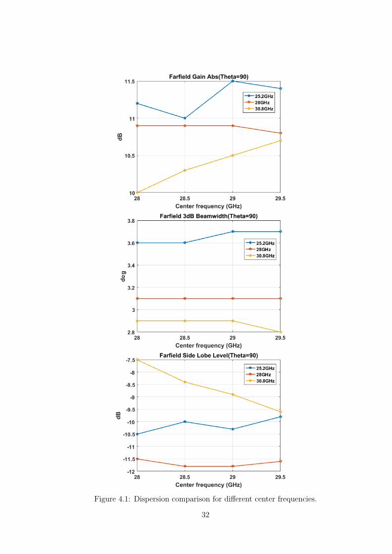
Figure 4.1: Dispersion comparison for different center frequencies.
32

Table 4.1: Far field of dielectric Luneburg lens with different design frequencies.
Designfrequency(GHz)
Frequency(GHz)
Main lobeGain Abs(dB)
3dB beamwidth()
Side lobelevel (dB)
2825.2 11.2 3.6 -10.528 10.9 3.1 -11.530.8 10 2.9 -7.5
28.525.2 11 3.6 -1028 10.9 3.1 -11.830.8 10.3 2.9 -8.4
2925.2 11.5 3.7 -10.328 10.9 3.1 -11.830.8 10.5 2.9 -8.9
29.525.2 11.4 3.7 -9.828 10.8 3.1 -11.630.8 10.7 2.8 -9.6
4.2 Metasurface Lens Design
Since the lens has two metasurface layers in glide symmetry, we would like to figure
out a way to manufacture them identically. If we simply shift one layer by half period,
the counterpart unit cells in two layers will have different distance to the origin, thus
different neff will there be according to Luneburg lens’s formula n =√
2− (ρ/R)2. To
solve this problem, the construction will keep both layers centered 1/4 period away
from the origin, as is shown in Figure 4.2.
In Figure 4.2, the blue gridding is the top layer while the red one is the bottom. Sys-
tem coordinate is settled at the origin marked with red and green arrow axes. Both
layers are shifted 1/4 period in x- and y- directions (marked in u- and v- in Figure
4.2), that we can simply flip one layer over a −45 axis (black dashed line) to obtain
the other one. Thus the we only need to manufacture one model twice instead of two
different models.
The metasurface model is generated in Ansys Electronic Desktop (HFSS) with HFSS-
API (application programming interface) controlled from Matlab. Taking the gap in
between two layers as a rectangular aperture, the radius of metasurface Luneburg
33

Figure 4.2: Wire frame view of two glide-symmetric layers.
lens is decided from a 3 dB beam width formula [29]:
∆θ = 51λ
aperature width. (4.1)
Since our requirement of 3 dB beam width is 5, the Luneburg lens diameter, equiva-
lent to aperture width in Equation 4.1, will be 2R = 10λ ≈ 107mm. With a loop pro-
gram, 878 unit cells are created in each layer. The appearance of one layer is presented
in Figure 4.3, where a discrete port is set at r = 56 mm instead of r = R ≈ 53 mm
because the Luneburg lens radius R measures the distance from outermost unit cell’s
center to origin, yet the feeding should be on the outside of outermost unit cell’s edge.
Figure 4.3: One layer of the glide-symmetric metasurface lens.
34

Figure 4.4: E-field in x-y plane.
The model is simulated in CST MWS Transient Solver, and we got E-field in the x-y
plane as shown in Figure 4.4. Spherical waves were emitted from the discrete port,
and got transferred into plane wave through the Luneburg lens. However, we cannot
see the reflection coefficient or far field now because the boundaries around the gap
are perfectly matched layers, that neither reflection will happen at the border nor any
far field will be generated. Therefore, the next step is to design a flare in between the
antenna aperture and free space, and set boundaries as Open (add space) in CST, to
simulate the real conditions of the antenna.
35

Chapter 5
Flare and Feeding Design
In order for the Luneburg lens antenna to work in real life, two other components
need to be designed apart from the metasurface lens. They are a matching flare at
the end of lens, and a practical feeding. A flare can greatly decrease the reflection
problem at the edge of lens, as the height of aperture could gradually increase thus
no sudden impedance variation occurs at the border. A practical feeding is what we
can use in real life, as the discrete port we adopted in Chapter 4 is just a physical
concept, not a feeding in reality. In the end, the overall performance of the antenna
should take all components into consideration, hence all parts should be matched well
apart from having good performance on themselves.
5.1 Flare Design
5.1.1 A Sliced Model
The flare contains six sectors. Seven points are set and optimized in CST instead
of assigning numerous points following a math curve. Experience proves that this
is completely enough for an appropriate flare. To save simulation time, instead of
optimizing the complete flare structure on the metasurface lens, we considered a slice
of PEC parallel plate with flare as shown in Figure 5.1. The red dots are where the
variable points lie, and a waveguide port is set as feeding in parallel plate aperture.
The gap height in between parallel plate is the same as the one in the metasurface lens.
First we have PMC boundary condition on two cut-sides of the slice, thus the waves
propagating inside parallel plate will be TEM, as the aperture has PMC boundaries
on left and right, and PEC on top and bottom. The plane wave will incident normally
on the edge of flare, which is one situation the flare will face in the lens antenna. The
36

Figure 5.1: A slice of parallel plate with flare.
Figure 5.2: Reflection coefficient of a sliced flare.
slice can be as thin as possible in this case.
Another situation is to have PEC boundary on two sides, then the aperture will
become a waveguide. The slice width must be appropriate in this case, thus the
designed frequency range will not be below cut-off, and only one mode exists. As is
known, the fundamental mode inside a waveguide is TE10, and it will go forward in a
zig-zag way since the waveguide wavelength is always longer than that in free space.
The formula of waveguide wavelength is given in Equation 5.1, where λ0 is free space
wavelength, and λc stands for cut-off wavelength of the waveguide. When the wave
arrives at the edge of flare, we have oblique incidence.
λguide =λ0√
1−(λ0λc
)2(5.1)
Taking both situations into account, a flare outside circular parallel plate with feed
at edge is equivalently simulated. The seven points are optimized to achieve the best
37

(a) top view
(b) side view
Figure 5.3: Circular parallel plate with the flare.
performance, leading to a flare length a = 20.91 mm, flare thickness b = 3.18 mm as
given in Figure 5.1. In Figure 5.2, the optimal reflection coefficient of both conditions
is given. In our needed frequency band marked with green bar, S11 of oblique incidence
is below -15 dB, and for normal incidence it is below -20 dB.
5.1.2 Flare with Circular Parallel Plate
To make sure the flare works well with our metasurface lens, further exploration was
done. We combined the optimized flare with a circular parallel plate of the same di-
mensions as the designed metasurface Luneburg lens. A waveguide port is placed at
the edge of the parallel plate, as is shown in Figure 5.3. The diameter of the circular
plate is 116 mm, while the radial length of the flare is 20.91 mm, less than 2λ at 28
GHz. The gap in between the two layers remains 0.3 mm. The waveguide port width
is 8.5 mm, whose cut-off frequency is about 17.6 GHz.
The reflection coefficient is presented in Figure 5.4, with our frequency band marked
with green bar. Ripples should be due to small reflections from the flare, since their
frequency interval matches the distance from waveguide port to the edge of flare. The
reflection coefficient is below -20 dB in our frequency range, meeting the requirements
perfectly. Electric field in x-y plane is also shown in Figure 5.5, where bare fluctuation
at the edge of the flare indicates that the flare is working fine.
38

Figure 5.4: Reflection coefficient of circular parallel plate with flare.
Figure 5.5: E-field in x-y plane at 28 GHz.
39

(a) top view of bottom layer
(b) side view
Figure 5.6: Metasurface lens with the flare.
5.1.3 Flare with Metasurface Lens
One last thing we checked is the combination of metasurface Luneburg lens and flare.
Since the above investigations already verified the feasibility of the flare, it would
be interesting to see how it works along with the lens. The diameter of lens part is
116 mm, same as that of circular parallel plate in last section, but longer than the
calculated one (with value equal to 107 mm) in Chapter 4.2. The reason is, first, the
diameter covered by the unit cells is longer than calculated diameter of unit cells’
center positions; second, a length of parallel plate is added outside of the lens, in
order to keep some adjusting margin for practical feeding. The model is shown in
Figure 5.6, and reflection coefficient is given in Figure 5.7. We can see the reflection
coefficient is below -17 dB in designed frequency band.
5.2 Feeding Design
The power source for antenna is coaxial feed line, but it could not be implemented
with the lens properly. Therefore, we need to design a transition component to
joint the probe and the lens. The component includes two parts, a coaxial probe to
rectangular waveguide transition section, and a stepped horn to connect the waveguide
and lens aperture. Full structure is given in Figure 5.8, and the two parts are designed
separately.
40

Figure 5.7: Reflection coefficient of metasurface lens with flare.
Figure 5.8: Feeding structure, x-y cut plane view.
41

Figure 5.9: Coaxial Probe data sheet.
5.2.1 Coaxial Probe to Rectangular Waveguide
Initially we want to use standard coaxial probe to waveguide transition element, like
waveguide WR28. However, the relatively large flange requires a long waveguide in
front of it to maintain multiple feedings around the lens, that we can test the scanning
capability. Hence, a self-designed feeding is finally adopted. The coaxial probe is from
Rosenberger company, and the data sheet drawings are illustrated in Figure 5.9. It
has no dielectric around the metal pin, so we need to design the thickness of air
surrounding the pin to achieve approximately 50 Ω impedance. The formula is
Z0 = 138 log
[Dout
Din
· 1√εr
](5.2)
where Din is the diameter of metal probe, and Dout being the diameter of dielectric.
Here we have air, hence the relative permittivity εr equals 1. The pin diameter is
1.27 mm as seen from Figure 5.9, hence Dout is calculated to be 2.9 mm to provide
49.5 Ω impedance.
The width of the waveguide is the same as the corresponding one of WR28, 7.112
mm, and the height is half of the corresponding one of WR28, being 1.778 mm. TE10
mode cut-off frequency is 21.1 GHz. Two irises are added to match the impedance
of coaxial probe and waveguide, as shown in Figure 5.10. The irises, located in the
42

(a) top view of x-y cut plane
(b) side view of x-z cut plane
Figure 5.10: Coaxial probe to waveguide transition structure.
transverse plane of magnetic field, can be taken as inductive shunt elements across the
waveguide, and the inductance is directly related to the size of iris itself. Similarly,
if an iris is placed within electric field, it is considered a conductive element. Irises
can be susceptible to break down under high power conditions, especially the electric
plane ones since they concentrate electric field. Hence in our design, only magnetic
plane irises are employed.
There are 6 parameter under optimization. L, K are the location of coaxial probe in
x- and y- direction, H is the height of metal pin in z- direction. For the two identical
irises, there are 3 parameters, length IrisX, width IrisY and position IrisP . The
corners are all smoothed to mimic real product appearance from milling technique.
In these parameters, IrisP is preliminarily estimated from impedance Smith Chart.
As shown in Figure 5.10, a waveguide port is set at the interface between waveg-
uide and stepped horn, named Port2. If we observe the impedance Smith Chart of
S22 and de-embed it for a proper distance, we can get a more concentrated relative
impedance curve that could be shifted closer to origin by simply adding some induc-
43

(a) on reference plane (b) on estimated iris plane without iris
(c) on estimated iris plane with 2 irises (d) on reference plane with 2 irises
Figure 5.11: Coaxial to waveguide transition, S-parameter impedance view.
tive impedance. This distance is how far the irises are from reference plane (Port2
surface). The comparison of S22 impedance views are demonstrated in Figure 5.11.
After adding two irises on the estimated iris plane, the impedance curve changed from
subgraph (b) to subgraph (c), encircling and being closer to the origin that stands
for perfect matching.
The reason why we could achieve a more compact curve just by moving towards load
is due to the different rotation angles on Smith Chart at different frequencies. Along
a lossless transmission line, the reflection coefficient is
Γ = ΓL exp(−2jβl) (5.3)
44

Figure 5.12: Stepped horn structure, x-z cut plane view.
where ΓL is the reflection coefficient at the load, and l is the length from the load back
to the measuring location. Since phase constant β relates to frequency, the change
rate will be different throughout given frequency band. The impedance curve rotates
faster at high frequencies than at low frequencies. Hence an expanded curve (a) can
turn into a more compact one (b), making it easier to match with shunt elements.
5.2.2 Stepped Horn Connection
The stepped horn connects the coaxial probe-waveguide component and the meta-
surface lens. It is designed with 3 steps as shown in the red frame in Figure 5.12.
The rightmost section has height g equal to the gap thickness of the lens, and length
d1. The next two sections have height g + t2 and g + t2 + t3 respectively, and length
d2, d3. Waveguide to the left of section 3 is the waveguide designed in Chapter 5.2.1,
whose height is 1.778 mm in z- direction. All five parameters in red are optimized,
aiming to match the waveguide and lens aperture perfectly. After optimization, the
total length d1 + d2 + d3 of the stepped horn is 10.84 mm. The impedance view of
reflection coefficient in Smith Chart is shown in Figure 5.13, where the reflection is
very small as the curve embraces the origin tightly.
After assembling the waveguide and stepped horn together, the total reflection coef-
ficient is below -20 dB as shown in Figure 5.14.
45

Figure 5.13: Stepped horn, S-parameter impedance view.
Figure 5.14: Reflection coefficient of whole feeding.
46

Chapter 6
Complete Design Results
In this chapter, metasurface lens, flare and feeding are assembled together into a full
antenna. The correct feed position is investigated, and multiple feedings are arranged
to cover certain scanning angles. The reflection, crosstalk, electric field and radiation
pattern are all presented.
6.1 Focal Point Determination
The appearance of integrated antenna is shown in Figure 6.1. The red dot is where
the feeding aperture is. Its location is varied from r = 56 mm to r = 58 mm to
determine the best focal point. Far field directivity, side lobe level, and 3 dB beam
width are all compared at different frequencies as presented in Figure 6.2.
Figure 6.1: Bottom layer of integrated lens.
47

Figure 6.2: Far field comparison of different feed position.
48

Figure 6.3: Electric field in x-y plane at 28 GHz, for full lens with one feeding.
Table 6.1: Far field performance of full lens with one feeding.
Frequency (GHz) 25.2 28 30.8
Main lobe Gain Abs (dB) 16.7 18.2 19.2
3dB beam width 6.6 5.7 5.0
Side lobe level (dB) −14.5 −18.5 −16.8
When r = 57.5 mm, the directivity and 3dB beam width are both optimized at all
three frequencies in a global aspect, while side lobe level is also one of the best choices.
Hence the joint feeding will be implemented at r = 57.5 mm.
6.2 Single Feeding Result
The full antenna was simulated in both CST Transient Solver and Frequency Solver,
to double check the results. Electric field and reflection coefficient are presented in
Figure 6.3 and 6.4 respectively. The electric field in Figure 6.4 proves the feasibility
of the integrated antenna. Near-spherical waves generated in waveguide feeding are
transformed into plane waves after the lens and got transmitted properly by the flare.
In Figure 6.3, we could see S11 in different solvers matches well, and is below -16
dB in the required frequency range. Far field at three typical frequencies are also
plotted in Figure 6.5, with detailed data given in Table 6.1. Comparing with Table
1.1 in Chapter 1, the beam width is a little bit larger than specified value 5, but still
acceptable. All results verified the validity of the design method.
49

Figure 6.4: Reflection coefficient of full lens with one feeding.
Figure 6.5: Far field Gain Abs (θ = 90) of full lens with one feeding.
50

Figure 6.6: Bottom layer of full lens with 11 ports.
Figure 6.7: Enlarged view of adjacent feedings and probe flanges.
6.3 Multiple Feedings Result
Further exploration is about the scanning capability, that is, the performance of the
Luneburg lens antenna with multiple feedings. The required scan range is ±60, but
due to implementation constraints, primarily space required for waveguide feeds, a
scan range of ±50 was selected.
The configuration is shown in Figure 6.6, where 11 feedings are arranged from −50
to 50 with 10 separation, and opening sector of the flare is from −55 to 55. The
angles are with respect to y- axis because now the symmetry axis is x- and flipping
51

Figure 6.8: Reflection coefficient of all 11 ports.
axis is y. Port 6 is the central feeding. The beam cross-over level is preliminarily cal-
culated to be around -8 dB. The reason why feedings have different waveguide lengths
is a consideration of fabrication. Since coaxial probe in Figure 5.9 is to be connected
to every waveguide, we need to leave enough space for its flange and manual screwing.
The enlarged view of two adjacent feeds is given in Figure 6.7.
The reflection coefficient of all ports are plotted in Figure 6.8. Solid curves are of
short waveguides, and coppery dashed curves are of long waveguides. Clearly same
waveguides at different positions have very similar profiles, and all of them are below
-16 dB in our frequency band of interest. Typical crosstalk between feedings are also
presented in Figure 6.9, where S2,1, S6,1, S11,1 are compared, and S3,2 is also given
since adjacent feedings face the highest crosstalk level. We can see that S2,1 and S3,2
are both below -21 dB.
The radiation pattern at three typical frequencies are also illustrated in Figure 6.10.
The cross-over level between beams is about -10 dB. 11 ports are excited at three
different frequencies, and the degree Phi in Figure 6.10 is with respect to y- axis.
Since the metasurface lens is not exactly isotropic, and with the influence of adjacent
ports and incomplete flare, every beam has asymmetric side lobes, except the middle
beam from Port 6.
52

Figure 6.9: Crosstalk between typical feedings.
53

Figure 6.10: Far field Gain Abs (θ = 90) at different frequencies.
54

Chapter 7
Tolerance Evaluation
The antenna will be manufactured in-house in Ericsson Kista with Aluminum. Before
that, some tolerance evaluation needs to be done for the information of mechanical
engineers, and to check the feasibility of this design.
One of the most important factors in fabrication is that the waveguide part will be
sealed as a whole, and the cavities will be milled on the bulk of metal. Another crucial
aspect is the gap g in between the two layers. We need to make sure it remains stable
over the whole lens area, but it might be difficult unless some washers are used.
7.1 Feeding Parameters Investigation
Before performing a parameter investigation, the corners of stepped horn are smoothed
under the proposal of the mechanical engineer, since they will also be manufactured
through milling. The new appearance is presented in Figure 7.1. No evident electro-
magnetic change happens, as seen in Figure 7.2.
Figure 7.1: x-y cut plane view of stepped horn.
55

Figure 7.2: S11 impedance view comparison of round- and sharp-corner stepped horn.
(a) top view of x-y cut plane
(b) side view of x-z cut plane
Figure 7.3: Coaxial probe to waveguide transition structure.
56

The perfect parameters for the self-designed feeding in Figure 7.3 (same as the one
in Chapter 5) are:
L = 2.27 mm K = 0 mm H = 1.22 mm
IrisX = 0.42 mm IrisY = 0.32 mm IrisP = 7.45 mm
Since the coaxial probe needs to be installed manually, its location might not be pre-
cisely where it is designed to be. Therefore, a parameter sweep is done for L,K and
H. Each of them are increased and decreased by 0.2 mm, and all other parameters
are kept constant during simulation. The reflection coefficient of the integrated feed-
ing accordingly is shown in Figure 7.4. As can be seen, the height H of probe is the
most critical, that requires extraordinarily careful operation. L and K have looser
requirements.
Another parameter suggested to investigate is the width of waveguide feeding. After a
similar parameter sweep procedure, the allowance is concluded to be (−0.1 mm,+0.4
mm) to make sure the reflection coefficient remains below -15 dB. The reason why
we cannot allow smaller value is due to cut-off of the waveguide. At smaller width,
the cut off frequency is too close to our lower frequency limit 25.2 GHz, and the
performance deteriorates rapidly.
7.2 Flare edge Smoothness Investigation
Since the lens is designed to be stacked in a pile which will allow for vertical steering,
the edge of flare is preferably smoothed rather than sharp as in Figure 5.1. The radius
of mellow edge is 0.5 mm, and a stacked flare slice is given in Figure 7.5. It contains
a middle model, bottom layer of the model above, and top layer of the model below.
The modified reflection coefficient with PEC and PMC boundaries are given in Fig-
ure 7.6. It can be seen that though curve shape changed, S11 with PEC boundaries
(oblique incidence) is still below -15 dB, and with PMC boundaries (normal inci-
dence), it is below -20 dB.
57

Figure 7.4: Tolerance Evaluation of coaxial probe’s location.
58

Figure 7.5: A stacked slice of parallel plate with flare.
Figure 7.6: Comparison of a sliced flare with different edges.
59

(a) Bottom layer with a washer.(b) Electric field in x-y plane at 28 GHz.
Figure 7.7: Model demonstration.
Table 7.1: Far field performance of one feeding lens with a washer.
Frequency (GHz) 25.2 28 30.8
Main lobe Gain Abs (dB) 17.5 18.1 18.2
3dB beam width 6 5.4 5.1
Side lobe level (dB) −13.8 −12.1 −11.8
7.3 Gap Height Investigation
The gap g in between the two layers must be kept constant to achieve the best per-
formance. Usually thin foams can be used, but in this design we want no dielectric
and the gap is too thin for a robust foam to fit. Hence we could introduce a screw
or washer inside the gap, but diffraction will happen and the wavefront might get
ruined. Another method is to not use a washer but let the antenna be, and find out
at what value of g will the behavior deteriorates.
First, a 2 mm radius Nylon P66 (εr ≈ 4) cylinder is defined at the front side of the
gap, as is shown in magenta Figure 7.7 (a). The electric field get distorted to a certain
extent as in Figure 7.7 (b), and its far field at three typical frequencies is plotted in
Figure 7.8. The detailed radiation patterns are listed in Table 7.1. We can see that
the side lobe level is already poor that we cannot accept any larger washer radius.
Another method is to use no upholder, just let the sealed feeding part support the
60

Figure 7.8: Far field Gain Abs (θ = 90) with a washer.
Table 7.2: Far field performance of one feeding lens with different g.
g = 0.26 mm g = 0.34 mm
Frequency (GHz) 25.2 28 30.8 25.2 28 30.8
Main lobe Gain Abs (dB) 17.5 17.9 17.7 16.2 17.5 18.7
3dB beam width 6.3 6.2 6.7 7.4 6.5 5.6
Side lobe level (dB) −15.5 −16.6 −17.3 −11.5 −12.8 −15.0
two layers. This situation is hard to simulate identically since the bending pattern
could be extremely complex, when we have one side fixed and the other side free.
Hence the model in CST is ajusted with a uniformly varied gap, and tolerance limit
is checked during the variation of g.
The largest acceptable change is 0.04 mm after investigation, which means g must
be between 0.26 mm and 0.34 mm if it varies uniformly. Though this is not the real
situation, we can get the feeling of how thick we can accept and let the real height
be in this range although the lens bends complexly. The electric field and reflection
coefficient for different values of g are shown in Figure 7.9 and Figure 7.10. And
radiation pattern with details are given in Figure 7.11 and Table 7.2 respectively.
61

(a) g = 0.26 mm. (b) g = 0.34 mm.
Figure 7.9: Electric field in x-y plane at 28 GHz.
Figure 7.10: Reflection coefficient at different values of g.
62

(a) g = 0.26 mm.
(b) g = 0.34 mm.
Figure 7.11: Far field Gain Abs (θ = 90) with different g.
63

Chapter 8
Conclusions and Future Work
In this thesis, a low-profile 2D metasurface Luneburg lens antenna is designed. It is
all-metal, with two glide-symmetric layers and flares, as well as 11 waveguide feeding
ports. The antenna performs well from 25.2 GHz to 30.8 GHz, showing a reflection
coefficient smaller than -15 dB, and crosstalk lower than -20 dB. The beam width
in the whole frequency range varies from 6.6 to 5, satisfying the requirement. The
tolerances of lens are also estimated for the easiness of manufacturing. It can be seen
that the air gap thickness between the two layers is the most critical one and might
need further handling. When material is set as lossy Aluminum, whose electric con-
ductivity equals 3.56× 10⁷ S/m, the loss in metal is about 12% of accepted power in
simulation, corresponding to 10 log10(1− 12%) = -0.555 dB variance in realized gain,
as can be seen from Figure 8.1 and Table 8.1.
The future work includes the fabrication of the whole lens and measuring. We can
test the prototype’s performance without a gap upholder since the feeding sector will
be sealed as a solid, providing quite steady support. Otherwise we can employ a
small washer at the other side of the lens to sustain the lens even more. Further
optimization can also be done for potential mass production, such as a better feeding
method to provide larger angular coverage and higher beam cross-over level, or a
smarter way to keep the whole metasurface lens antenna more stable and decrease
Table 8.1: Realized gain comparison between Aluminum lens and PEC lens.
Frequency (GHz) 25.2 28 30.8
PEC lens (dB) 17.7 18.7 19.2
Aluminum lens (dB) 17.2 18.2 18.6
64

Figure 8.1: Powers in metasurface lens of Aluminum.
the leakage from feed assembling, or even change the manufacturing method from
milling to plastic molding for a better unit cell solution, as there are less need of
considering practical processing difficulty.
65

Bibliography
[1] R. K. Luneburg. Mathematical Theory of Optics. Brown University Press, 1944.
[2] C. Pfeiffer and A. Grbic. A printed, broadband luneburg lens antenna. IEEE
Trans. Antennas Propag., 58(9):3055–3059, Sept 2010.
[3] G. D. M. Peeler and H. P. Coleman. Microwave Stepped-Index Luneberg Lenses.
IRE TRansactions on Antennas and Propagation, (April):202–207, 1958.
[4] S. R. Baev, S. M. Gechev, B. N. Hadjistamov, and P. I. Dankov. Modelling and
Simulations of Luneburg Lens Antennas for Communication Purposes. Telecom-
munications forum FELFOR, (August):488–491, 2008.
[5] G. Peeler and D. Archer. A Two-Dimensional Microwave Luneberg Lens. Trans-
actions of the IRE Professional Group on Antennas and Propagation, 1(1):12–23,
1952.
[6] K. Sato and H. Ujiie. A plate Luneberg lens with the permittivity distribution
controlled by hole density. Electronics and Communications in Japan, Part
I: Communications (English translation of Denshi Tsushin Gakkai Ronbunshi),
85(9):1–12, 2002.
[7] L. Xue and V. F. Fusco. 24 ghz automotive radar planar luneburg lens. IET
Microwaves, Antennas Propagation, 1(3):624–628, June 2007.
[8] J. Reinholdt. Cylindrical Luneburg Lens Antenna for Multi-Beam Small Cell
Wireless Backhaul Applications. Master’s thesis, Ericsson AB, LTU, 2014.
[9] Q. Cheng, H. F. Ma, and T. J. Cui. Broadband planar Luneburg lens based on
complementary metamaterials. Applied Physics Letters, 95(18):181901, 2009.
[10] M. G. Silveirinha, C. A. Fernandes, and J. R. Costa. Electromagnetic charac-
terization of textured surfaces formed by metallic pins. IEEE Trans. Antennas
Propag., 56(2):405–415, 2008.
66

[11] M. Casaletti, F. Caminita, and S. Maci. A luneburg lens designed by using
a variable artificial surface. In 2010 IEEE Antennas and Propagation Society
International Symposium, pages 1–4, July 2010.
[12] M. Bosiljevac, M. Casaletti, F. Caminita, Z. Sipus, and S. Maci. Non-uniform
metasurface luneburg lens antenna design. IEEE Trans. Antennas Propag.,
60(9):4065–4073, Sept 2012.
[13] X. Xiong, Y. Liu, Z. Yao, L. Zhang, W. Li, and Q. H. Liu. Design of a metasurface
luneburg lens antenna with flared structure. In Proceedings of 2014 3rd Asia-
Pacific Conference on Antennas and Propagation, pages 375–378, July 2014.
[14] J. A. Dockrey, M. J. Lockyear, S. J. Berry, S. A. R. Horsley, J. R. Sambles, and
A. P. Hibbins. Thin metamaterial Luneburg lens for surface waves. Physical
Review B - Condensed Matter and Materials Physics, 87(12):1–5, 2013.
[15] O. Quevedo-Teruel, M. Ebrahimpouri, and M. Ng Mou Kehn. Ultrawideband
metasurface lenses based on off-shifted opposite layers. IEEE Antennas Wireless
Propag. Lett., 15:484–487, Dec 2016.
[16] A. Torki, M. Ebrahimpouri, and O. Quevedo-Teruel. A planar steerable 60
ghz leaky wave antenna with luneburg lens feed. In 2016 IEEE International
Symposium on Antennas and Propagation (APSURSI), pages 1405–1406, June
2016.
[17] M. Ebrahimpouri, O. Quevedo-Teruel, and E. Rajo-Iglesias. Design Guidelines
for Gap Waveguide Technology Based on Glide-Symmetric Holey Structures.
IEEE Microw. Compon. Lett., 27(6):542–544, June 2017.
[18] M. Ebrahimpouri, E. Rajo-Iglesias, Zvonimir Sipus, and O. Quevedo-Teruel.
Cost-effective gap waveguide technology based on glide-symmetric holey ebg
structures. accepted in IEEE Trans. Microw. Theory Techn., 2017.
[19] K. Liu, F. Ghasemifard, and O. Quevedo-Teruel. Broadband metasurface luneb-
urg lens antenna based on glide-symmetric bed of nails. In 2017 11th European
Conference on Antennas and Propagation (EuCAP), pages 358–360, March 2017.
[20] O. Luukkonen, C. Simovski, G. Granet, G. Goussetis, D. Lioubtchenko, A. V.
Raisanen, and S. A. Tretyakov. Simple and accurate analytical model of planar
grids and high-impedance surfaces comprising metal strips or patches. IEEE
Trans. Antennas Propag., 56(6):1624–1632, 2008.
67

[21] S. Maci, G. Minatti, M. Casaletti, and M. Bosiljevac. Metasurfing: Addressing
waves on impenetrable metasurfaces. IEEE Antennas Wireless Propag. Lett.,
10:1499–1502, 2011.
[22] H. T. Chen, A. J. Taylor, and N. Yu. A review of metasurfaces: physics and
applications. Reports on Progress in Physics, page 076401, 2016.
[23] A. Hessel, M. H. Chen, R. C. M. Li, and A. A. Oliner. Propagation in periodically
loaded waveguides with higher symmetries. Proceedings of the IEEE, 61(2):183–
195, Feb 1973.
[24] O. Dahlberg, R. C. Mitchell-Thomas, and O. Quevedo-Teruel. Reducing the
dispersion of periodic structures with twist and polar glide symmetries. Scientific
Reports, 7(10136):2045–2322, 2017.
[25] M. Camacho, R. C. Mitchell-Thomas, A. P. Hibbins, J. R. Sambles, and
O. Quevedo-Teruel. Designer surface plasmon dispersion on a one-dimensional
periodic slot metasurface with glide symmetry. Opt. Lett., 42(17):3375–3378, Sep
2017.
[26] G. Valerio, Z. Sipus, A. Grbic, and O. Quevedo-Teruel. Accurate equivalent-
circuit descriptions of thin glide-symmetric corrugated metasurfaces. IEEE
Trans. Antennas Propag., 65(5):2695–2700, May 2017.
[27] F. Ghasemifard, M. Ebrahimpouri, M. Norgren, and O. Quevedo-Teruel. Mode
matching analysis of two dimensional glide-symmetric corrugated metasurfaces.
In 2017 11th European Conference on Antennas and Propagation (EuCAP),
pages 749–751, March 2017.
[28] Fatemeh Ghasemifard, Martin Norgren, and Oscar Quevedo-Terue. Disper-
sion analysis of two dimensional glide-symmetric corrugated metasurfaces using
mode-matching technique. submitted to IEEE Microw. Compon. Lett., 2017.
[29] S. J. Orfanidis. Electromagnetic Waves and Antennas. Rutguers University,
2016.
68