integrated luneburg lens via ultra-strong index … · integrated luneburg lens via ultra-strong...
TRANSCRIPT
Integrated Luneburg lens viaultra-strong index gradient on silicon
Lucas H. Gabrielli1 and Michal Lipson1,2,*
1Cornell Nanophotonics Group, School of Electrical and Computer Engineering,Cornell University, Ithaca, New York 14853, USA
2Kavli Institute at Cornell, Cornell University, Ithaca, New York 14853, USA
Abstract: Gradient index structures are gaining increased importance withthe constant development of Transformation Optics and metamaterials. Ourability to fabricate such devices, while limited, has already demonstrated theextensive capabilities of those designs, in the forms of invisibility devices,as well as illusion optics and super-lensing. In this paper we present a lowloss, high index contrast lens that is integrated with conventional nanopho-tonic waveguides to provide improved tolerance in fiber-to-chip opticallinks for future communication networks. This demonstration representsa positive step in making the extraordinary capabilities of gradient indexdevices available for integrated optics.
© 2011 Optical Society of America
OCIS codes: (110.2760) Gradient-index lenses; (230.3120) Integrated optics devices.
References and links1. D. Smith, J. Mock, A. Starr, and D. Schurig, “Gradient index metamaterials,” Phys. Rev. E 71, 036609 (2005).2. R. B. Greegor, C. G. Parazzoli, J. A. Nielsen, M. A. Thompson, M. H. Tanielian, and D. R. Smith, “Simulation
and testing of a graded negative index of refraction lens,” Appl. Phys. Lett. 87, 091114 (2005).3. T. Driscoll, D. N. Basov, A. F. Starr, P. M. Rye, S. Nemat-Nasser, D. Schurig, and D. R. Smith, “Free-space
microwave focusing by a negative-index gradient lens,” Appl. Phys. Lett. 88, 081101 (2006).4. L. H. Gabrielli, J. Cardenas, C. B. Poitras, and M. Lipson, “Silicon nanostructure cloak operating at optical
frequencies,” Nat. Photonics 3, 461–463 (2009).5. J. Valentine, J. Li, T. Zentgraf, G. Bartal, and X. Zhang, “An optical cloak made of dielectrics,” Nat. Mater. 8,
568–571 (2009).6. R. Liu, X. M. Yang, J. G. Gollub, J. J. Mock, T. J. Cui, and D. R. Smith, “Gradient index circuit by waveguided
metamaterials,” Appl. Phys. Lett. 94, 073506 (2009).7. K. Preston, N. Sherwood-Droz, J. S. Levi, H. L. R. Lira, and M. Lipson, “Design rules for WDM optical inter-
connects using silicon microring resonators,” (2011), submitted to Opt. Express.8. R. K. Luneburg, Mathematical Theory of Optics (University of California Press, 1964).9. U. Leonhardt and T. Philbin, Geometry and Light: The Science of Invisibility (Dover Publications, 2010).
10. T. Shoji, T. Tsuchizawa, T. Watanabe, K. Yamada, and H. Morita, “Low loss mode size converter from 0.3 μmsquare Si wire waveguides to singlemode fibres,” Electron. Lett. 38, 1669 (2002).
11. V. R. Almeida, R. R. Panepucci, and M. Lipson, “Nanotaper for compact mode conversion,” Opt. Lett. 28, 1302(2003).
12. K. K. Lee, D. R. Lim, D. Pan, C. Hoepfner, W.-Y. Oh, K. Wada, L. C. Kimerling, K. P. Yap, and M. T. Doan,“Mode transformer for miniaturized optical circuits,” Opt. Lett. 30, 498 (2005).
13. G. Roelkens, P. Dumon, W. Bogaerts, D. Van Thourhout, and R. Baets, “Efficient silicon-on-insulator fiber cou-pler fabricated using 248-nm-deep UV lithography,” IEEE Photon. Technol. Lett. 17, 2613–2615 (2005).
14. A. Di Falco, S. C. Kehr, and U. Leonhardt, “Luneburg lens in silicon photonics,” Opt. Express 19, 5156 (2011).15. F. Zernike, “Luneburg lens for optical waveguide use,” Opt. Commun. 12, 379–381 (1974).16. N. Kundtz and D. R. Smith, “Extreme-angle broadband metamaterial lens,” Nat. Mater. 9, 129–32 (2010).17. H. F. Ma and T. J. Cui, “Three-dimensional broadband and broad-angle transformation-optics lens,” Nat. Com-
mun. 1, 124 (2010).
#151750 - $15.00 USD Received 25 Jul 2011; revised 7 Sep 2011; accepted 22 Sep 2011; published 29 Sep 2011(C) 2011 OSA 10 October 2011 / Vol. 19, No. 21 / OPTICS EXPRESS 20122
18. T. Zentgraf, Y. Liu, M. H. Mikkelsen, J. Valentine, and X. Zhang, “Plasmonic Luneburg and Eaton lenses,” NatureNanotechnol. 6, 151–155 (2011).
19. J. Cardenas, C. B. Poitras, J. T. Robinson, K. Preston, L. Chen, and M. Lipson, “Low loss etchless silicon photonicwaveguides,” Opt. Express 17, 4752 (2009).
1. Introduction
Gradient index (GRIN) structures have received increased attention in recent literature, frominvisibility cloaks and illusion devices, to planar lenses, such as Maxwell’s fish eye. Fabricationof such structures, where the dielectric medium is modified rapidly on a few-wavelength scale,is challenging and limited by scattering loses introduced by discrete elements often used inthe effective media [1–6]. We show here a low loss GRIN structure based on ultra-strong indexvariation with unique index variation profiles over 30µm that drastically improves the toleranceof conventional fiber-to-waveguide links—a critical aspect for enabling future optical networkson chip [7]. The ability to fabricate GRIN structures with ultra-strong gradient can enable awhole new class of photonic devices with new functionalities for light propagation, opticalsignal processing, and imaging techniques in general.
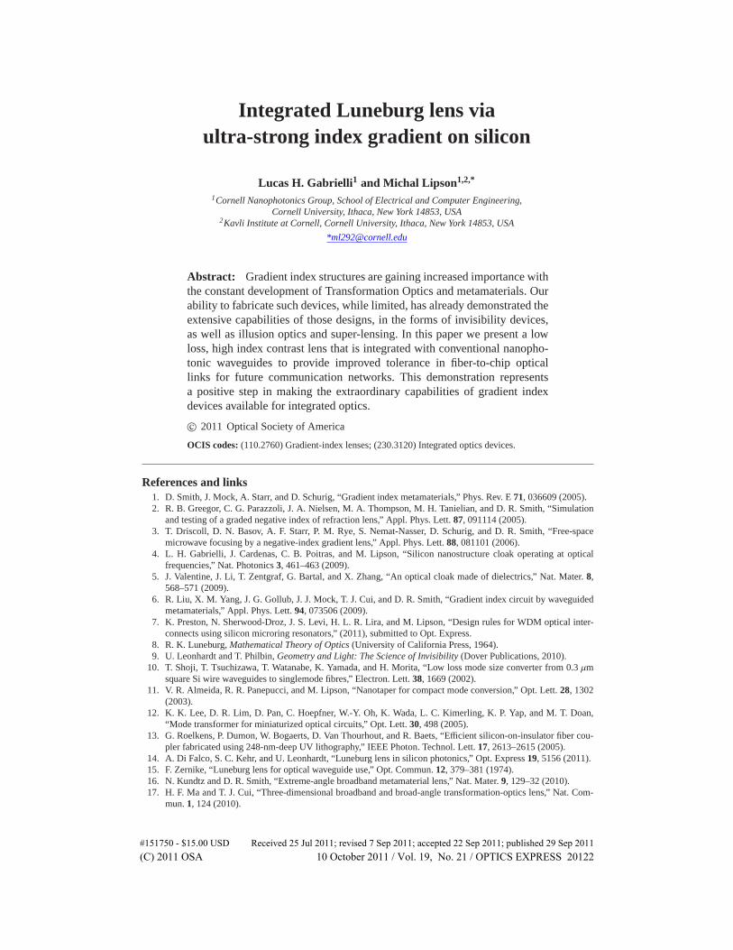
Among GRIN structures, the Luneburg lens is of special interest and can be demonstratedusing only dielectric materials. The Luneburg lens is an aberration-free and coma-free sphericallens whose focal points lie on a circumference around itself [8,9]. Rays incident from far away(i.e. with k vector parallel to the direction of propagation) at different positions will all focus onthe same point on the circumference (Fig. 1b). This is in strong contrast to a conventional lens,where, due to aberrations, the focal point varies with the position of the incident light (Fig. 1a).In addition, unlike a conventional lens, the Luneburg is composed of a rotationally symmetricgradient refractive index n2 = n2
0(2−ρ2), where n0 is constant and ρ is the normalized coordinatein the radial direction of the lens, shown in Fig. 1c. This way, one can choose the constant n0 tomatch the environment refractive index, and eliminate reflections at the lens interface.
The lack of sensitivity of the Luneburg lens to the exact position of the incoming lighthas strong applications for the robust coupling between photonic structures with very differ-ent scales. The integration of future optical communications from the fiber optical cable downto the microprocessor core will require efficient and reliable coupling devices, both at the fiber-to-chip and inter-chip levels. Low-loss, fiber-to-chip coupling can be achieved today via inversetappers [10–13], which adiabatically convert the large modes coming from optical fibers intothe tightly confined modes of integrated silicon waveguides. Nonetheless, to perform prop-erly, these tapers have stringent alignment requirements, due to their high sensitivity [11]. Theneed thus arises for passive optical couplers that are robust to misalignment—a class of de-vices designed to reliably collect the energy delivered to the chip and couple it to the system’swaveguides.
2. Design and fabrication
For applications in silicon photonics, the Luneburg lens is required to have a strong indexvariation over a short distance without introducing excessive loss. A Luneburg lens was recentlydemonstrated in silicon using a tapered waveguide for tailoring the index of refraction [14] by41% over a disk of 98µm radius. Here, in order to demonstrate a Luneburg lens for siliconphotonics we tailor the index by 41% over 15µm.
The gradient refractive index necessary for the Luneburg lens was implemented by control-ling the thickness of the guiding layer of the device [14]. Light confinement in the directionnormal to the device is achieved by total internal reflection between a guiding silicon layerand the top and bottom SiO2 claddings. The effective refractive index of this slab structure isdependent on the thickness of the silicon layer, such that the gradient refractive index required
#151750 - $15.00 USD Received 25 Jul 2011; revised 7 Sep 2011; accepted 22 Sep 2011; published 29 Sep 2011(C) 2011 OSA 10 October 2011 / Vol. 19, No. 21 / OPTICS EXPRESS 20123
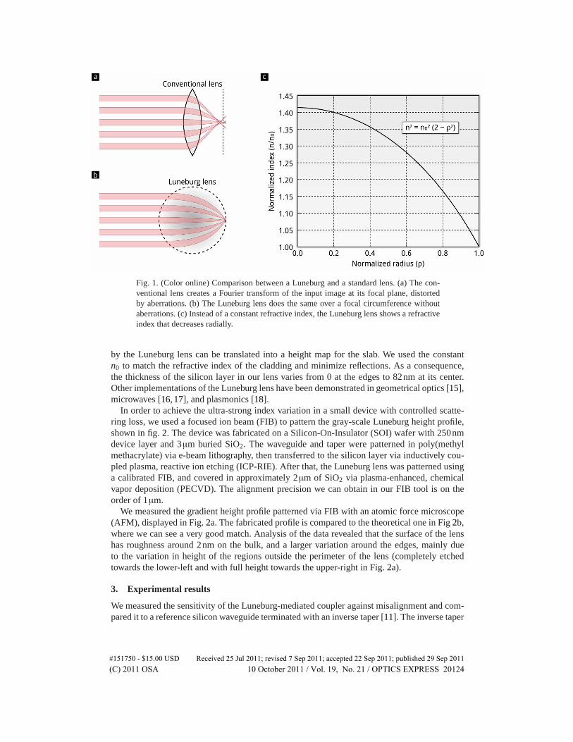
Fig. 1. (Color online) Comparison between a Luneburg and a standard lens. (a) The con-ventional lens creates a Fourier transform of the input image at its focal plane, distortedby aberrations. (b) The Luneburg lens does the same over a focal circumference withoutaberrations. (c) Instead of a constant refractive index, the Luneburg lens shows a refractiveindex that decreases radially.
by the Luneburg lens can be translated into a height map for the slab. We used the constantn0 to match the refractive index of the cladding and minimize reflections. As a consequence,the thickness of the silicon layer in our lens varies from 0 at the edges to 82nm at its center.Other implementations of the Luneburg lens have been demonstrated in geometrical optics [15],microwaves [16, 17], and plasmonics [18].
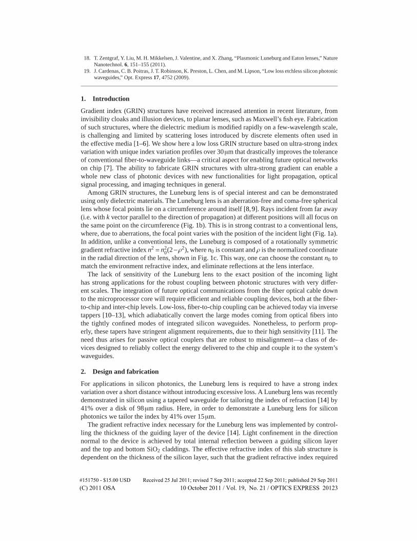
In order to achieve the ultra-strong index variation in a small device with controlled scatte-ring loss, we used a focused ion beam (FIB) to pattern the gray-scale Luneburg height profile,shown in fig. 2. The device was fabricated on a Silicon-On-Insulator (SOI) wafer with 250nmdevice layer and 3µm buried SiO2. The waveguide and taper were patterned in poly(methylmethacrylate) via e-beam lithography, then transferred to the silicon layer via inductively cou-pled plasma, reactive ion etching (ICP-RIE). After that, the Luneburg lens was patterned usinga calibrated FIB, and covered in approximately 2µm of SiO2 via plasma-enhanced, chemicalvapor deposition (PECVD). The alignment precision we can obtain in our FIB tool is on theorder of 1µm.
We measured the gradient height profile patterned via FIB with an atomic force microscope(AFM), displayed in Fig. 2a. The fabricated profile is compared to the theoretical one in Fig 2b,where we can see a very good match. Analysis of the data revealed that the surface of the lenshas roughness around 2nm on the bulk, and a larger variation around the edges, mainly dueto the variation in height of the regions outside the perimeter of the lens (completely etchedtowards the lower-left and with full height towards the upper-right in Fig. 2a).
3. Experimental results
We measured the sensitivity of the Luneburg-mediated coupler against misalignment and com-pared it to a reference silicon waveguide terminated with an inverse taper [11]. The inverse taper
#151750 - $15.00 USD Received 25 Jul 2011; revised 7 Sep 2011; accepted 22 Sep 2011; published 29 Sep 2011(C) 2011 OSA 10 October 2011 / Vol. 19, No. 21 / OPTICS EXPRESS 20124
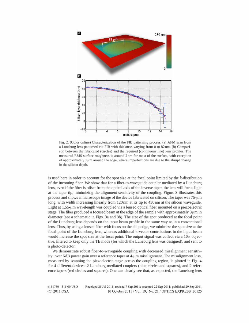
Fig. 2. (Color online) Characterization of the FIB patterning process. (a) AFM scan froma Luneburg lens patterned via FIB with thickness varying from 0 to 82nm. (b) Compari-son between the fabricated (circles) and the required (continuous line) lens profiles. Themeasured RMS surface roughness is around 2nm for most of the surface, with exceptionof approximately 1µm around the edge, where imperfections are due to the abrupt changein the silicon depth.
is used here in order to account for the spot size at the focal point limited by the k-distributionof the incoming fiber. We show that for a fiber-to-waveguide coupler mediated by a Luneburglens, even if the fiber is offset from the optical axis of the inverse taper, the lens will focus lightat the taper tip, minimizing the alignment sensitivity of the coupling. Figure 3 illustrates thisprocess and shows a microscope image of the device fabricated on silicon. The taper was 75-µmlong, with width increasing linearly from 120nm at its tip to 450nm at the silicon waveguide.Light at 1.55-µm wavelength was coupled via a lensed optical fiber mounted on a piezoelectricstage. The fiber produced a focused beam at the edge of the sample with approximately 3µm indiameter (see a schematic in Figs. 3a and 3b). The size of the spot produced at the focal pointof the Luneburg lens depends on the input beam profile in the same way as in a conventionallens. Thus, by using a lensed fiber with focus on the chip edge, we minimize the spot size at thefocal point of the Luneburg lens, whereas additional k-vector contributions in the input beamwould increase the spot size at the focal point. The output signal was collect via a 10× objec-tive, filtered to keep only the TE mode (for which the Luneburg lens was designed), and sent toa photo-detector.
We demonstrate robust fiber-to-waveguide coupling with decreased misalignment sensitiv-ity: over 6dB power gain over a reference taper at 4-µm misalignment. The misalignment loss,measured by scanning the piezoelectric stage across the coupling region, is plotted in Fig. 4for 4 different devices: 2 Luneburg-mediated couplers (blue circles and squares), and 2 refer-ence tapers (red circles and squares). One can clearly see that, as expected, the Luneburg lens
#151750 - $15.00 USD Received 25 Jul 2011; revised 7 Sep 2011; accepted 22 Sep 2011; published 29 Sep 2011(C) 2011 OSA 10 October 2011 / Vol. 19, No. 21 / OPTICS EXPRESS 20125

Fig. 3. (Color online) Fiber-to-chip coupler based on the Luneburg lens. (a) A lensed fiberis used to couple light into the silicon waveguide. (b) Zoomed-in illustration of the couplingregion. We add a Luneburg lens to the conventional inverse taper design to minimize lossesinduced by the misalignment Δ. (c) Optical microscope image of the fabricated device.The trenches defining the waveguide and taper are due to the use of positive resist. Thevariation of the silicon layer thickness in the lens can be clearly seen by the interferencepattern (colors) in the image. Note that the dark area on the left edge of the image is due toface polishing, i.e., the lens has not been damaged.
decreases the losses introduced by misalignment. Note, however, that these measurements arenormalized by the power detected with no misalignment for each device, at which position thetotal insertion loss of the Luneburg-mediated couplers was approximately 6.5dB higher thanthe reference. We believe that the fabrication process is responsible for this additional insertionloss. The FIB patterning introduces partial amorphization of the silicon layer, as well as gal-lium implantation, and a small roughness on the surface of the lens, which in principle could bedecreased using annealing and controlled oxidation [19]. Additionally, misalignment betweenthe lens and the inverse taper may also increase the insertion loss, but this could be mitigatedwith improved alignment control in the patterning tool.
The continuous lines in Fig. 4 are results from full 3-d simulations performed with COMSOLMultiphysics®. The simulation includes a lens with the same diameter as the tested device,plus the taper region, and a Gaussian source with standard deviation σ = 3µm placed 1µmfrom the device input facet (in air). The simulated results showed that the inclusion of theLuneburg lens has no fundamental impact in the total insertion loss of our structure, confirmingour expectations that the additional losses are due to imperfections in the fabrication, and theyshow a good match for the alignment sensitivity.
4. Conclusion
Silicon-based compact GRIN structures, including the demonstrated here Luneburg-mediatedcoupler, pave the way to a class of ultra-compact GRIN devices with novel photonic propertiesincluding aberration-free imaging, advanced optical signal processing, and mode multiplexing
#151750 - $15.00 USD Received 25 Jul 2011; revised 7 Sep 2011; accepted 22 Sep 2011; published 29 Sep 2011(C) 2011 OSA 10 October 2011 / Vol. 19, No. 21 / OPTICS EXPRESS 20126
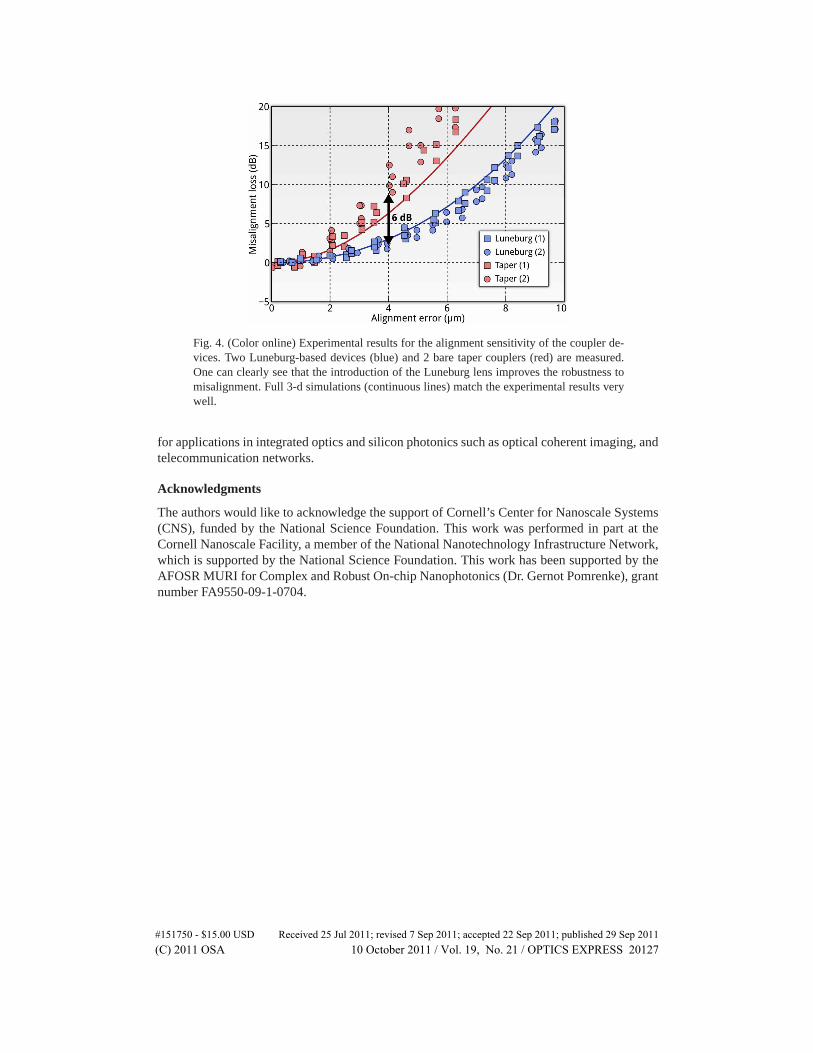
Fig. 4. (Color online) Experimental results for the alignment sensitivity of the coupler de-vices. Two Luneburg-based devices (blue) and 2 bare taper couplers (red) are measured.One can clearly see that the introduction of the Luneburg lens improves the robustness tomisalignment. Full 3-d simulations (continuous lines) match the experimental results verywell.
for applications in integrated optics and silicon photonics such as optical coherent imaging, andtelecommunication networks.
Acknowledgments
The authors would like to acknowledge the support of Cornell’s Center for Nanoscale Systems(CNS), funded by the National Science Foundation. This work was performed in part at theCornell Nanoscale Facility, a member of the National Nanotechnology Infrastructure Network,which is supported by the National Science Foundation. This work has been supported by theAFOSR MURI for Complex and Robust On-chip Nanophotonics (Dr. Gernot Pomrenke), grantnumber FA9550-09-1-0704.
#151750 - $15.00 USD Received 25 Jul 2011; revised 7 Sep 2011; accepted 22 Sep 2011; published 29 Sep 2011(C) 2011 OSA 10 October 2011 / Vol. 19, No. 21 / OPTICS EXPRESS 20127