isolated power supplies made easy - analog.com · 38 | january 2011 : lt journal of analog...
TRANSCRIPT
38 | January 2011 : LT Journal of Analog Innovation
Isolated Power Supplies Made EasyJohn D. Morris
One challenge in designing a flyback
converter is that information relating to
the output voltage on the secondary side
of the transformer must be fed back to the
regulator on the primary side in order to
maintain regulation. Historically, feedback
across the isolation barrier is achieved
using opto-isolators or extra transformer
windings, though both methods present a
number of design problems. Opto-isolator
feedback circuits add components, increas-
ing converter size and cost. They also draw
power, degrading efficiency and complicat-
ing thermal design. Opto-isolators also
make it difficult to accurately regulate
the output due to their limited dynamic
response, inherent nonlinearities, typical
variation from unit-to-unit and varia-
tion with age. The usual alternative is
to add an extra transformer winding,
but this may introduce other problems,
including bigger, more expensive mag-
netics or limited dynamic response.
By contrast, the LT3748 infers the
isolated output voltage by examin-
ing the primary-side flyback pulse
waveform. In this manner, neither an
opto-isolator nor an extra transformer
winding is required to maintain regula-
tion, and the output voltage is easily
programmed with two resistors.
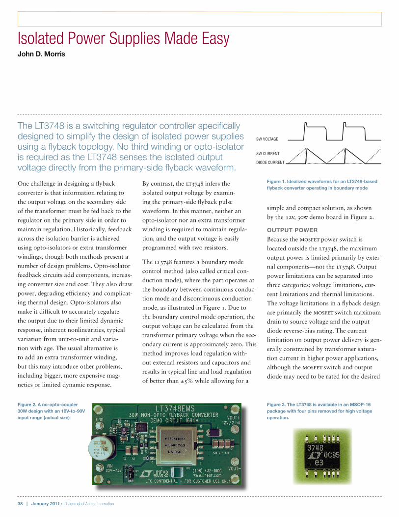
The LT3748 features a boundary mode
control method (also called critical con-
duction mode), where the part operates at
the boundary between continuous conduc-
tion mode and discontinuous conduction
mode, as illustrated in Figure 1. Due to
the boundary control mode operation, the
output voltage can be calculated from the
transformer primary voltage when the sec-
ondary current is approximately zero. This
method improves load regulation with-
out external resistors and capacitors and
results in typical line and load regulation
of better than ±5% while allowing for a
simple and compact solution, as shown
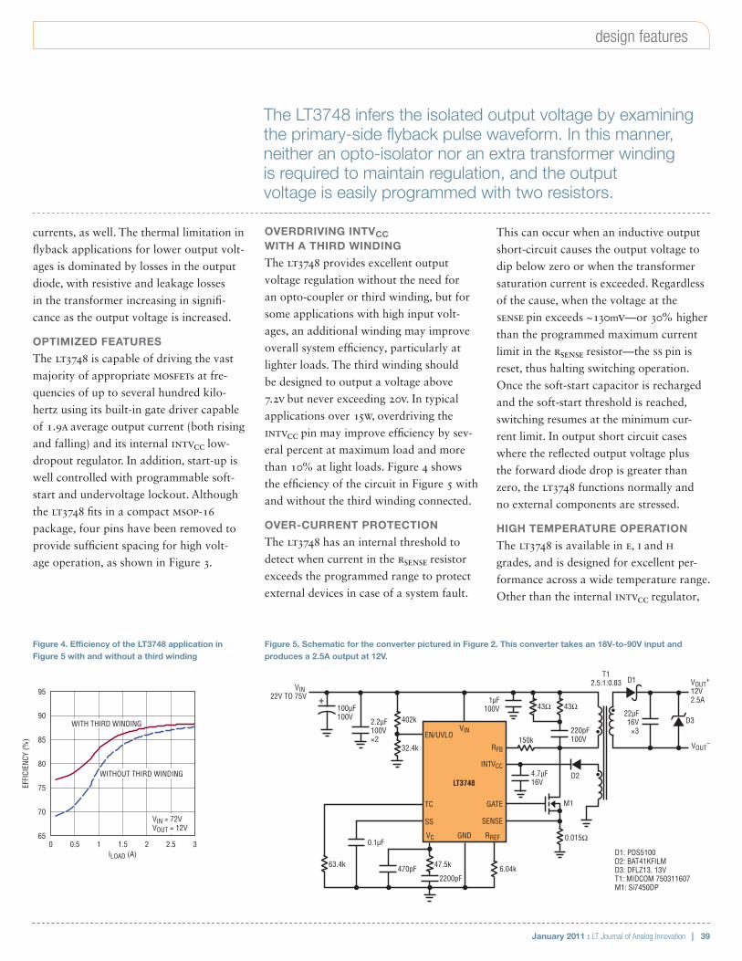
by the 12V, 30W demo board in Figure 2.
OUTPUT POWER
Because the MOSFET power switch is
located outside the LT3748, the maximum
output power is limited primarily by exter-
nal components—not the LT3748. Output
power limitations can be separated into
three categories: voltage limitations, cur-
rent limitations and thermal limitations.
The voltage limitations in a flyback design
are primarily the MOSFET switch maximum
drain to source voltage and the output
diode reverse-bias rating. The current
limitation on output power delivery is gen-
erally constrained by transformer satura-
tion current in higher power applications,
although the MOSFET switch and output
diode may need to be rated for the desired
The LT3748 is a switching regulator controller specifically designed to simplify the design of isolated power supplies using a flyback topology. No third winding or opto-isolator is required as the LT3748 senses the isolated output voltage directly from the primary-side flyback waveform.
SW VOLTAGE
SW CURRENT
DIODE CURRENT
Figure 1. Idealized waveforms for an LT3748-based flyback converter operating in boundary mode
Figure 2. A no-opto-coupler 30W design with an 18V-to-90V input range (actual size)
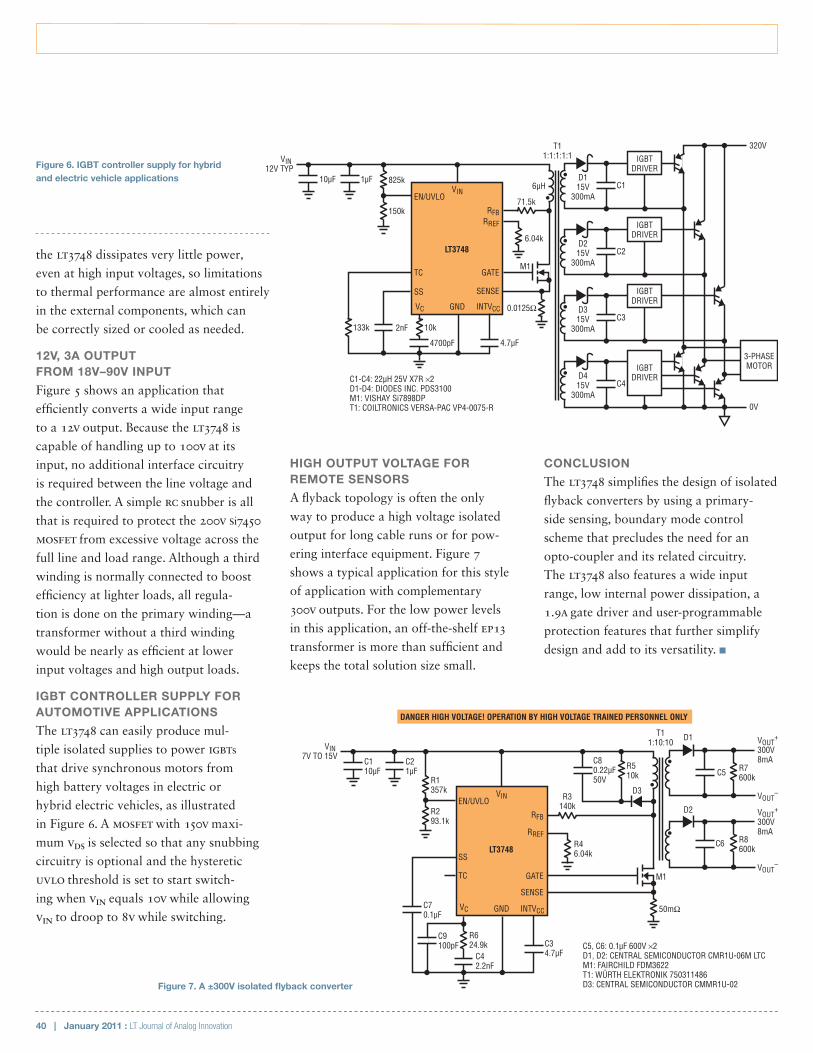
Figure 3. The LT3748 is available in an MSOP-16 package with four pins removed for high voltage operation.
January 2011 : LT Journal of Analog Innovation | 39
design features
currents, as well. The thermal limitation in
flyback applications for lower output volt-
ages is dominated by losses in the output
diode, with resistive and leakage losses
in the transformer increasing in signifi-
cance as the output voltage is increased.
OPTIMIZED FEATURES
The LT3748 is capable of driving the vast
majority of appropriate MOSFETs at fre-
quencies of up to several hundred kilo-
hertz using its built-in gate driver capable
of 1.9A average output current (both rising
and falling) and its internal INTVCC low-
dropout regulator. In addition, start-up is
well controlled with programmable soft-
start and undervoltage lockout. Although
the LT3748 fits in a compact MSOP-16
package, four pins have been removed to
provide sufficient spacing for high volt-
age operation, as shown in Figure 3.
OVERDRIVING INTVCC WITH A THIRD WINDING
The LT3748 provides excellent output
voltage regulation without the need for
an opto-coupler or third winding, but for
some applications with high input volt-
ages, an additional winding may improve
overall system efficiency, particularly at
lighter loads. The third winding should
be designed to output a voltage above
7.2V but never exceeding 20V. In typical
applications over 15W, overdriving the
INTVCC pin may improve efficiency by sev-
eral percent at maximum load and more
than 10% at light loads. Figure 4 shows
the efficiency of the circuit in Figure 5 with
and without the third winding connected.
OVER-CURRENT PROTECTION
The LT3748 has an internal threshold to
detect when current in the RSENSE resistor
exceeds the programmed range to protect
external devices in case of a system fault.
This can occur when an inductive output
short-circuit causes the output voltage to
dip below zero or when the transformer
saturation current is exceeded. Regardless
of the cause, when the voltage at the
SENSE pin exceeds ~130mV—or 30% higher
than the programmed maximum current
limit in the RSENSE resistor—the SS pin is
reset, thus halting switching operation.
Once the soft-start capacitor is recharged
and the soft-start threshold is reached,
switching resumes at the minimum cur-
rent limit. In output short circuit cases
where the reflected output voltage plus
the forward diode drop is greater than
zero, the LT3748 functions normally and
no external components are stressed.
HIGH TEMPERATURE OPERATION
The LT3748 is available in E, I and H
grades, and is designed for excellent per-
formance across a wide temperature range.
Other than the internal INTVCC regulator,
EFFI
CIEN
CY (%
)
ILOAD (A)30
95
650.5 1 1.5 2 2.5
70
75
85
80
90
VIN = 72VVOUT = 12V
WITH THIRD WINDING
WITHOUT THIRD WINDING
Figure 4. Efficiency of the LT3748 application in Figure 5 with and without a third winding
EN/UVLO
TC
SS
RFB
INTVCC
VC GND RREF
LT3748
63.4k
0.1µF
VIN 22V TO 75V
VOUT+
12V2.5A
VIN
T12.5:1:0.83
D2
D1
402k
32.4k
100µF100V 22µF
16V×3
GATE
SENSE
2.2µF100V×2
1µF100V
2200pF470pF
M1
6.04k
D3
0.015Ω
VOUT–
47.5k
220pF100V
4.7µF16V
43Ω43Ω
150k
+
D1: PDS5100D2: BAT41KFILMD3: DFLZ13, 13VT1: MIDCOM 750311607M1: Si7450DP
Figure 5. Schematic for the converter pictured in Figure 2. This converter takes an 18V-to-90V input and produces a 2.5A output at 12V.
The LT3748 infers the isolated output voltage by examining the primary-side flyback pulse waveform. In this manner, neither an opto-isolator nor an extra transformer winding is required to maintain regulation, and the output voltage is easily programmed with two resistors.
40 | January 2011 : LT Journal of Analog Innovation
CONCLUSION
The LT3748 simplifies the design of isolated
flyback converters by using a primary-
side sensing, boundary mode control
scheme that precludes the need for an
opto-coupler and its related circuitry.
The LT3748 also features a wide input
range, low internal power dissipation, a
1.9A gate driver and user-programmable
protection features that further simplify
design and add to its versatility. n
HIGH OUTPUT VOLTAGE FOR REMOTE SENSORS
A flyback topology is often the only
way to produce a high voltage isolated
output for long cable runs or for pow-
ering interface equipment. Figure 7
shows a typical application for this style
of application with complementary
300V outputs. For the low power levels
in this application, an off-the-shelf EP13
transformer is more than sufficient and
keeps the total solution size small.
the LT3748 dissipates very little power,
even at high input voltages, so limitations
to thermal performance are almost entirely
in the external components, which can
be correctly sized or cooled as needed.
12V, 3A OUTPUT FROM 18V–90V INPUT
Figure 5 shows an application that
efficiently converts a wide input range
to a 12V output. Because the LT3748 is
capable of handling up to 100V at its
input, no additional interface circuitry
is required between the line voltage and
the controller. A simple RC snubber is all
that is required to protect the 200V Si7450
MOSFET from excessive voltage across the
full line and load range. Although a third
winding is normally connected to boost
efficiency at lighter loads, all regula-
tion is done on the primary winding—a
transformer without a third winding
would be nearly as efficient at lower
input voltages and high output loads.
IGBT CONTROLLER SUPPLY FOR AUTOMOTIVE APPLICATIONS
The LT3748 can easily produce mul-
tiple isolated supplies to power IGBTs
that drive synchronous motors from
high battery voltages in electric or
hybrid electric vehicles, as illustrated
in Figure 6. A MOSFET with 150V maxi-
mum VDS is selected so that any snubbing
circuitry is optional and the hysteretic
UVLO threshold is set to start switch-
ing when VIN equals 10V while allowing
VIN to droop to 8V while switching.
EN/UVLO
TC
SS
RFBRREF
VC GND INTVCC
LT3748
133k 2nF
VIN 12V TYP
VIN
T11:1:1:1:1
D115V
300mA
825k
150k
10µF6µH C1
GATE
SENSE
1µF
4700pF 4.7µF
6.04k
71.5k
0.0125Ω
M1
10k
IGBTDRIVER
D215V
300mAC2
IGBTDRIVER
D315V
300mAC3
IGBTDRIVER
D415V
300mA
C1-C4: 22µH 25V X7R ×2D1-D4: DIODES INC. PDS3100M1: VISHAY Si7898DPT1: COILTRONICS VERSA-PAC VP4-0075-R
C4
IGBTDRIVER
320V
0V
3-PHASEMOTOR
Figure 6. IGBT controller supply for hybrid and electric vehicle applications
EN/UVLO
TC
SS
RFB
RREF
VC GND INTVCC
LT3748
R624.9k
VIN 7V TO 15V
VOUT+
300V8mA
VOUT+
300V8mA
VOUT–VIN
T11:10:10
R1357k
R293.1k
C110µF C5
GATE
SENSE
C21µF
C70.1µF
C42.2nF
C9100pF C3
4.7µF
R46.04k
R3140k
R510k
R7600k
R8600k
D1
DANGER HIGH VOLTAGE! OPERATION BY HIGH VOLTAGE TRAINED PERSONNEL ONLY
D3
50mΩ
M1VOUT
–
C6
C80.22µF50V
D2
C5, C6: 0.1µF 600V ×2D1, D2: CENTRAL SEMICONDUCTOR CMR1U-06M LTCM1: FAIRCHILD FDM3622T1: WÜRTH ELEKTRONIK 750311486D3: CENTRAL SEMICONDUCTOR CMMR1U-02Figure 7. A ±300V isolated flyback converter