isl78840aseh, isl78841aseh, isl78843aseh ... 1mhz and high peak current drive capability with 50ns...
TRANSCRIPT
FN7952Rev 2.00
Feb 23, 2018
ISL78840ASxH, ISL78841ASxH, ISL78843ASxH, ISL78845ASxHRadiation Hardened, High Performance Industry Standard Single-Ended Current Mode PWM Controller
DATASHEET
The ISL78840ASEH, ISL78841ASEH, ISL78843ASEH, ISL78845ASEH, ISL78840ASRH, ISL78841ASRH, ISL78843ASRH, ISL78845ASRH are high performance, radiation hardened drop-in replacements for the popular 28C4x and 18C4x PWM controllers suitable for a wide range of power conversion applications including boost, flyback, and isolated output configurations. Fast signal propagation and output switching characteristics make these ideal products for existing and new designs.
Features include up to 13.2V operation, low operating current, 90µA typical start-up current, adjustable operating frequency to 1MHz and high peak current drive capability with 50ns rise and fall times.
Applications• Current mode switching power supplies
• Isolated buck and flyback regulators
• Boost regulators
• Direction and speed control in motors
• Control of high current FET drivers
Related LiteratureFor a full list of related documents, visit our website
• ISL78840ASEH, ISL78841ASEH, ISL78843ASEH, ISL78845ASEH, ISL78840ASRH, ISL78841ASRH, ISL78843ASRH, and ISL78845ASRH product pages
Features• Electrically screened to DLA SMD #5962-07249
• QML qualified per MIL-PRF-38535 requirements
• 1A MOSFET gate driver
• 90µA typical start-up current, 125µA maximum
• 35ns propagation delay current sense to output
• Fast transient response with peak current-mode control
• 9V to 13.2V operation
• Adjustable switching frequency to 1MHz
• 50ns rise and fall times with 1nF output load
• Trimmed timing capacitor discharge current for accurate dead time/maximum duty cycle control
• 1.5MHz bandwidth error amplifier
• Tight tolerance voltage reference over line, load, and temperature
• ±3% current limit threshold
• Pb-free available (RoHS compliant)
• Radiation environment:
- High dose rate (50 - 300rad(Si)/s). . . . . . . . . . 100krad(Si)
- Low dose rate (0.01rad(Si)/s) . . . . . . . . . . . . 100krad(Si)*
* Product capability established by initial characterization. The “EH” version is acceptance tested on a wafer-by-wafer basis to 50krad(Si) at low dose rate. (Applies to ISL7884xASEH only)
TABLE 1. KEY DIFFERENCES BETWEEN FAMILY OF PARTS
PART NUMBERRISING UVLO
(V)MAXIMUM DUTY CYCLE
(%)
ISL78840ASxH 7.0 100
ISL78841ASxH 7.0 50
ISL78843ASxH 8.4 100
ISL78845ASxH 8.4 50
FN7952 Rev 2.00 Page 1 of 17Feb 23, 2018

ISL78840ASxH, ISL78841ASxH, ISL78843ASxH, ISL78845ASxH
Ordering InformationORDERING NUMBER
(Note 1)PART NUMBER
(Note 2)TEMP. RANGE
(°C)PACKAGE
(RoHS Compliant) PKG. DWG. #
5962R0724905VPC ISL78840ASEHVD -55 to +125 8 Ld SBDIP D8.3
5962R0724906VPC ISL78841ASEHVD -55 to +125 8 Ld SBDIP D8.3
5962R0724907VPC ISL78843ASEHVD -55 to +125 8 Ld SBDIP D8.3
5962R0724908VPC ISL78845ASEHVD -55 to +125 8 Ld SBDIP D8.3
5962R0724905VXC ISL78840ASEHVF -55 to +125 8 Ld Flatpack K8.A
5962R0724906VXC ISL78841ASEHVF -55 to +125 8 Ld Flatpack K8.A
5962R0724907VXC ISL78843ASEHVF -55 to +125 8 Ld Flatpack K8.A
5962R0724908VXC ISL78845ASEHVF -55 to +125 8 Ld Flatpack K8.A
5962R0724905V9A ISL78840ASEHVX -55 to +125 Die
5962R0724906V9A ISL78841ASEHVX -55 to +125 Die
5962R0724907V9A ISL78843ASEHVX -55 to +125 Die
5962R0724908V9A ISL78845ASEHVX -55 to +125 Die
5962R0724901V9A ISL78840ASRHVX -55 to +125 Die
ISL78840ASRHX/SAMPLE (Note 3) -55 to +125 Die
ISL78840ASRHF/PROTO (Note 3) -55 to +125 8 Ld Flatpack K8.A
5962R0724901QXC ISL78840ASRHQF -55 to +125 8 Ld Flatpack K8.A
5962R0724901VXC ISL78840ASRHVF -55 to +125 8 Ld Flatpack K8.A
ISL78840ASRHD/PROTO (Note 3) -55 to +125 8 Ld SBDIP D8.3
5962R0724901QPC ISL78840ASRHQD -55 to +125 8 Ld SBDIP D8.3
5962R0724901VPC ISL78840ASRHVD -55 to +125 8 Ld SBDIP D8.3
5962R0724902V9A ISL78841ASRHVX -55 to +125 Die
ISL78841ASRHX/SAMPLE (Note 3) -55 to +125 Die
ISL78841ASRHF/PROTO (Note 3) -55 to +125 8 Ld Flatpack K8.A
5962R0724902QXC ISL78841ASRHQF -55 to +125 8 Ld Flatpack K8.A
5962R0724902VXC ISL78841ASRHVF -55 to +125 8 Ld Flatpack K8.A
ISL78841ASRHD/PROTO (Note 3) -55 to +125 8 Ld SBDIP D8.3
5962R0724902QPC ISL78841ASRHQD -55 to +125 8 Ld SBDIP D8.3
5962R0724902VPC ISL78841ASRHVD -55 to +125 8 Ld SBDIP D8.3
5962R0724903V9A ISL78843ASRHVX -55 to +125 Die
ISL78843ASRHX/SAMPLE (Note 3) -55 to +125 Die
ISL78843ASRHF/PROTO (Note 3) -55 to +125 8 Ld Flatpack K8.A
5962R0724903QXC ISL78843ASRHQF -55 to +125 8 Ld Flatpack K8.A
5962R0724903VXC ISL78843ASRHVF -55 to +125 8 Ld Flatpack K8.A
ISL78843ASRHD/PROTO (Note 3) -55 to +125 8 Ld SBDIP D8.3
5962R0724903QPC ISL78843ASRHQD -55 to +125 8 Ld SBDIP D8.3
5962R0724903VPC ISL78843ASRHVD -55 to +125 8 Ld SBDIP D8.3
5962R0724904V9A ISL78845ASRHVX -55 to +125 Die
ISL78845ASRHX/SAMPLE (Note 3) -55 to +125 Die
ISL78845ASRHF/PROTO (Note 3) -55 to +125 8 Ld Flatpack K8.A
FN7952 Rev 2.00 Page 2 of 17Feb 23, 2018

ISL78840ASxH, ISL78841ASxH, ISL78843ASxH, ISL78845ASxH
5962R0724904QXC ISL78845ASRHQF -55 to +125 8 Ld Flatpack K8.A
5962R0724904VXC ISL78845ASRHVF -55 to +125 8 Ld Flatpack K8.A
ISL78845ASRHD/PROTO (Note 3) -55 to +125 8 Ld SBDIP D8.3
5962R0724904QPC ISL78845ASRHQD -55 to +125 8 Ld SBDIP D8.3
5962R0724904VPC ISL78845ASRHVD -55 to +125 8 Ld SBDIP D8.3
NOTES:
1. These Pb-free Hermetic packaged products employ 100% Au plate - e4 termination finish, which is RoHS compliant and compatible with both SnPb and Pb-free soldering operations.
2. Specifications for Rad Hard QML devices are controlled by the Defense Logistics Agency Land and Maritime (DLA). The SMD numbers listed in the “Ordering Information” table must be used when ordering.
3. The /PROTO and /SAMPLE are not rated or certified for Total Ionizing Dose (TID) or Single Event Effect (SEE) immunity. These parts are intended for engineering evaluation purposes only. The /PROTO parts meet the electrical limits and conditions across the temperature range specified in the DLA SMD and are in the same form and fit as the qualified device. The /SAMPLE die is capable of meeting the electrical limits and conditions specified in the DLA SMD at +25°C only. The /SAMPLE is a die and does not receive 100% screening across the temperature range to the DLA SMD electrical limits. These part types do not come with a certificate of conformance because there is no radiation assurance testing and they are not DLA qualified devices.
Ordering Information (Continued)
ORDERING NUMBER(Note 1)
PART NUMBER(Note 2)
TEMP. RANGE(°C)
PACKAGE(RoHS Compliant) PKG. DWG. #
Pin ConfigurationsISL78840ASEH, ISL78841ASEH, ISL78843ASEH, ISL78845ASEH ISL78840ASRH, ISL78841ASRH, ISL78843ASRH, ISL78845ASRH
(8 LD FLATPACK)TOP VIEW
ISL78840ASEH, ISL78841ASEH, ISL78843ASEH, ISL78845ASEH ISL78840ASRH, ISL78841ASRH, ISL78843ASRH, ISL78845ASRH
(8 LD SBDIP)TOP VIEW
8
7
6
5
2
3
4
1COMP
FB
CS
RTCT
VREF
VDD
OUT
GND
COMP
FB
CS
RTCT
1
2
3
4
8
7
6
5
VREF
VDD
OUT
GND
FN7952 Rev 2.00 Page 3 of 17Feb 23, 2018

ISL78840ASxH, ISL78841ASxH, ISL78843ASxH, ISL78845ASxH
Pin DescriptionsPIN NAME PIN NUMBER DESCRIPTION
RTCT 4 The oscillator timing control pin. The operational frequency and maximum duty cycle are set by connecting a resistor, RT, between VREF and this pin and a timing capacitor, CT, from this pin to GND. The oscillator produces a sawtooth waveform with a programmable frequency range up to 2.0MHz. The charge time, tC, the discharge time, tD, the RTCT oscillator frequency, f, and the maximum duty cycle, DMAX, can be approximated from Equations 1 through 4:
The formulas have increased error at higher frequencies due to propagation delays. Figure 7 may be used as a guideline in selecting the capacitor and resistor values required for a given oscillator frequency for the ISL7884xASxH. The switching frequency for the ISL78841ASxH and ISL78845ASxH will be half the RTCT oscillator frequency.
COMP 1 COMP is the output of the error amplifier and the input of the PWM comparator. The control loop frequency compensation network is connected between the COMP and FB pins.
FB 2 The output voltage feedback is connected to the inverting input of the error amplifier through this pin. The noninverting input of the error amplifier is internally tied to a reference voltage.
CS 3 The current sense input to the PWM comparator. The range of the input signal is nominally 0V to 1.0V and has an internal offset of 100mV.
GND 5 GND is the power and small signal reference ground for all functions.
OUT 6 The drive output to the power switching device. It is a high current output capable of driving the gate of a power MOSFET with peak currents of 1.0A. This GATE output is actively held low when VDD is below the UVLO threshold.
VDD 7 VDD is the power connection for the device. The total supply current will depend on the load applied to OUT. Total IDD current is the sum of the operating current and the average output current. Knowing the operating frequency, f and the MOSFET gate charge, Qg, the average output current can be calculated from Equation 5:
To optimize noise immunity, bypass VDD to GND with a ceramic capacitor as close to the VDD and GND pins as possible.
VREF 8 The 5.00V reference voltage output. +1.0/-1.5% tolerance over line, load and operating temperature. The recommended bypass to GND cap is in the range 0.1µF to 0.22µF. A typical value of 0.15µF can be used.
(EQ. 1)tC 0.533 RT CT
tD RT– CT In0.008 RT 3.83–0.008 RT 1.71–---------------------------------------------
(EQ. 2)
f 1 tC tD+ = (EQ. 3)
D tC f= (EQ. 4)
IOUT Qg f= (EQ. 5)
FN7952 Rev 2.00 Page 4 of 17Feb 23, 2018

FN
795
2R
ev 2
.00
Pag
e 5 of 17
Feb
23, 2
018
ISL7
884
0AS
xH, IS
L7
8841
AS
xH, IS
L78
843
AS
xH, IS
L7
8845
AS
xH
OUT
VREF
k
Functional Block Diagram
FIGURE 1. BLOCK DIAGRAM
TQ
Q
ON150k
100k
VDD
CS
FB
RTCT
GND
PWMCOMPARATOR
RESET DOMINANT
2.5V
ENABLE
8.4mA
2.9V1.0V
OSCILLATORCOMPARATOR
<10ns
+-
START/STOPUV COMPARATOR
VREF5V
+-
+-
100mV
ERROR AMPLIFIER
+-
VREF
+-
ON
+-
S
R
Q
Q
COMP
VREFUV COMPARATOR
4.65V 4.80V
+ -
A = 0.5
+-
CLOCK
1.1VCLAMP
2R
RVF TOTAL = 1.15V
A
VREF FAULT
OKVDD
36
ISL78841A,ONLY
ISL78845A

FN
795
2R
ev 2
.00
Pag
e 6 of 17
Feb
23, 2
018
ISL7
884
0AS
xH, IS
L7
8841
AS
xH, IS
L78
843
AS
xH, IS
L7
8845
AS
xH
RETURN
+1.8V
+3.3V
U3
16
C14
C13R15
R19
R17 R18
R20
C15 C16
C12
C11
+ +C21
C22
C20
+
Typical Application - 48V Input Dual Output Flyback
FIGURE 2. TYPICAL APPLICATION - 48V INPUT DUAL OUTPUT FLYBACK
VIN+
VIN-
T1
Q3
36V TO 75V
VR1
C1
C2
C3
R1
R3 C4
Q1
R4
CR6
C5
R22
U2
CR2
CR5
CR4
C17
R21
R
R13C8
R10R6
CR1
C19
+
C6
ISL7884xASxH
VDD
RTCT
CS
FB OUT
COMP VREF
GND
R26
R27
U4
R28
FN
795
2R
ev 2
.00
Pag
e 7 of 17
Feb
23, 2
018
ISL7
884
0AS
xH, IS
L7
8841
AS
xH, IS
L78
843
AS
xH, IS
L7
8845
AS
xH
C9
R7
2
C5
C3
VIN+
+VOUT
R6
R5
RETURN
C8
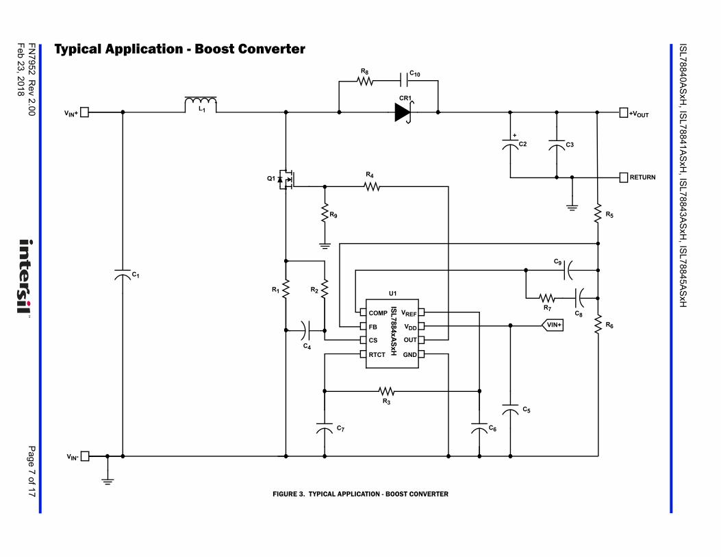
Typical Application - Boost Converter
FIGURE 3. TYPICAL APPLICATION - BOOST CONVERTER
VIN+
VIN-
C1
Q1
R1
R4
CR1
C
C6C7
R3
+
R2
C4
L1
U1
ISL
7884xAS
xH
OUTCS
RTCT
FB
COMP VREF
VDD
GND
C10R8
R9

ISL78840ASxH, ISL78841ASxH, ISL78843ASxH, ISL78845ASxH
Absolute Maximum Ratings Thermal InformationSupply Voltage VDD Without Beam . . . . . . . . . . . . . (GND -0.3V) to +30.0VSupply Voltage VDD Under Beam . . . . . . . . . . . . . . . (GND -0.3V) to +14.7VOUT . . . . . . . . . . . . . . . . . . . . . . . . . . . . . . . . . . . . . (GND -0.3V) to VDD + 0.3VSignal Pins . . . . . . . . . . . . . . . . . . . . . . . . . . . . . . . . . . . . (GND -0.3V) to 6.0VPeak GATE Current . . . . . . . . . . . . . . . . . . . . . . . . . . . . . . . . . . . . . . . . . . . . 1AESD Rating
Human Body Model (Tested per JESD22-A114E) . . . . . . . . . . . . . . . . 2kVMachine Model (Tested per JESD22-A115-A) . . . . . . . . . . . . . . . . . 200V
Latch-Up (Tested per JESD-78B; Class 2, Level A) . . . . . . . . . . . . . . 100mA
Recommended Operating ConditionsTemperature Range . . . . . . . . . . . . . . . . . . . . . . . . . . . . . . .-55°C to +125°CSupply Voltage (Typical Note 6) . . . . . . . . . . . . . . . . . . . . . . . . . 9V to 13.2V
Thermal Resistance (Typical) JA (°C/W) JC (°C/W)8 Ld Flatpack Package (Notes 4, 5) 140 158 Ld SBDIP Package (Notes 4, 5) 98 15
Maximum Junction Temperature . . . . . . . . . . . . . . . . . . . . . . . . . . . .+150°CStorage Temperature Range. . . . . . . . . . . . . . . . . . . . . . . .-65°C to +150°C
Radiation InformationMaximum Total Dose
Dose Rate = 50 - 100radSi/s . . . . . . . . . . . . . . . . . . . . . . . . 100krads (Si)Dose Rate = 0.01rad(Si)/s (Note 7) . . . . . . . . . . . . . . . . . . . 100krad (Si)
SEB (No Burnout) (Note 8) . . . . . . . . . . . . . . . . . . . . . . . . . . 80Mev/mg/cm2
SEL (No latch-up) (Note 8) . . . . . . . . . . . . . . . . . . . . . . . . . . 43Mev/mg/cm2
SET (Regulated VOUT within ±3%) (Note 8) . . . . . . . . . . . . 40Mev/mg/cm2
CAUTION: Do not operate at or near the maximum ratings listed for extended periods of time. Exposure to such conditions may adversely impact productreliability and result in failures not covered by warranty.
NOTES:
4. JA is measured with the component mounted on a low-effective thermal conductivity test board in free air. See TB379 for details.
5. For JC, the "case temp" location is the center of the ceramic on the package underside.
6. All voltages are with respect to GND.
7. Product capability established by initial characterization. The “EH” version is acceptance tested on a wafer-by-wafer basis to 50krad(Si) at low dose rate. (Applied only to ISL7884xASEH.)
8. SEE tests performed with VREF bypass capacitor of 0.22µF and fSW = 200kHz. SEB/L tests done on a standalone open loop configuration. SET tests done in a closed loop configuration. For LET ≤ 43MeV/mg•cm2. The SEL observed requiring a power cycle to recover operation occurred at ≤ 43MeV/mg•cm2 < LET ≤ 80MeV/mg•cm2. For more information see: ISL7884xASRH SEE Test Report.
Electrical Specifications Recommended operating conditions unless otherwise noted. Refer to Block Diagram on page 5 and Typical Application on page 6. VDD = 13.2V, RT = 10kΩ, CT = 3.3nF, TA = -55 to +125°C. Typical values are at TA = +25°C. Boldface limits apply across the operating temperature range, -55 to +125°C.
PARAMETER TEST CONDITIONSMIN
(Note 11) TYPMAX
(Note 11) UNIT
UNDERVOLTAGE LOCKOUT
START Threshold ISL78840A, ISL78841A 6.5 7.0 7.5 V
ISL78843A, ISL78845A 8.0 8.4 9.0 V
STOP Threshold ISL78840A, ISL78841A 6.1 6.6 6.9 V
ISL78843A, ISL78845A 7.3 7.6 8.0 V
Hysteresis ISL78840A, ISL78841A - 0.4 - V
ISL78843A, ISL78845A - 0.8 - V
Start-Up Current, IDD VDD < START Threshold - 90 125 µA
VDD < START Threshold, 100krad - 300 500 µA
Operating Current, IDD (Note 9) - 2.9 4.0 mA
Operating Supply Current, ID Includes 1nF GATE loading - 4.75 5.50 mA
REFERENCE VOLTAGE
Overall Accuracy Over line (VDD = 9V to 13.2V), load of 1mA and 10mA, temperature
4.925 5.000 5.050 V
Long Term Stability TA = +125°C, 1000 hours (Note 10) - 5 - mV
Current Limit, Sourcing -20 - - mA
Current Limit, Sinking 5 - - mA
CURRENT SENSE
Input Bias Current VCS = 1V -1.0 - 1.0 µA
FN7952 Rev 2.00 Page 8 of 17Feb 23, 2018

ISL78840ASxH, ISL78841ASxH, ISL78843ASxH, ISL78845ASxH
Input Signal, Maximum 0.97 1.00 1.03 V
Gain, ACS = VCOMP/VCS 0 < VCS < 910mV, VFB = 0V 2.75 2.82 3.15 V/V
CS to OUT Delay - 35 55 ns
ERROR AMPLIFIER
Open Loop Voltage Gain (Note 10) - 90 - dB
Unity Gain Bandwidth (Note 10) - 1.5 - MHz
Reference Voltage, VREF VFB = VCOMP 2.475 2.500 2.530 V
FB Input Bias Current, FBIIB VFB = 0V -1.0 -0.2 1.0 µA
COMP Sink Current VCOMP = 1.5V, VFB = 2.7V 1.0 - - mA
COMP Source Current VCOMP = 1.5V, VFB = 2.3V -0.4 - - mA
COMP VOH VFB = 2.3V 4.80 - VREF V
COMP VOL VFB = 2.7V 0.4 - 1.0 V
PSRR Frequency = 120Hz, VDD = 9V to 13.2V (Note 10)
- 80 - dB
OSCILLATOR
Frequency Accuracy Initial, TA = +25°C 48 51 53 kHz
Frequency Variation with VDD TA= +25°C, (f13.2V - f9V)/f12V - 0.2 1.0 %
Temperature Stability (Note 10) - 5 - %
Amplitude, Peak-to-Peak Static Test - 1.75 - V
RTCT Discharge Voltage (Valley Voltage) Static Test - 1.0 - V
Discharge Current RTCT = 2.0V 6.5 7.8 8.5 mA
OUTPUT
Gate VOH VDD to OUT, IOUT = -100mA - 1.0 2.0 V
Gate VOL OUT to GND, IOUT = 100mA - 1.0 2.0 V
Peak Output Current COUT = 1nF (Note 10) - 1.0 - A
Rise Time COUT = 1nF - 35 60 ns
Fall Time COUT = 1nF - 20 40 ns
OUTPUT OFF State Leakage VDD = 5V - - 50 µA
PWM
Maximum Duty Cycle (ISL78840A, ISL78843A)
COMP = VREF 94.096.0 - %
Maximum Duty Cycle(ISL78841A, ISL78845A)
COMP = VREF 47.048.0 - %
Minimum Duty Cycle COMP = GND - - 0 %
NOTES:
9. This is the VDD current consumed when the device is active but not switching. Does not include gate drive current.
10. Limits established by characterization and are not production tested.
11. Parameters with MIN and/or MAX limits are 100% tested at +25°C, unless otherwise specified. Temperature limits established by characterization and are not production tested.
Electrical Specifications Recommended operating conditions unless otherwise noted. Refer to Block Diagram on page 5 and Typical Application on page 6. VDD = 13.2V, RT = 10kΩ, CT = 3.3nF, TA = -55 to +125°C. Typical values are at TA = +25°C. Boldface limits apply across the operating temperature range, -55 to +125°C. (Continued)
PARAMETER TEST CONDITIONSMIN
(Note 11) TYPMAX
(Note 11) UNIT
FN7952 Rev 2.00 Page 9 of 17Feb 23, 2018
ISL78840ASxH, ISL78841ASxH, ISL78843ASxH, ISL78845ASxH
Functional DescriptionFeaturesThe ISL7884xASxHs’ current mode PWM makes an ideal choice for low-cost flyback and forward topology applications. With their greatly improved performance over industry standard parts, they are the obvious choice for new designs or existing designs, which require updating.
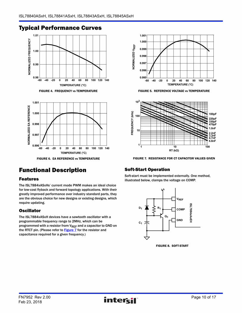
OscillatorThe ISL7884xASxH devices have a sawtooth oscillator with a programmable frequency range to 2MHz, which can be programmed with a resistor from VREF and a capacitor to GND on the RTCT pin. (Please refer to Figure 7 for the resistor and capacitance required for a given frequency.)
Soft-Start OperationSoft-start must be implemented externally. One method, illustrated below, clamps the voltage on COMP.
Typical Performance Curves
FIGURE 4. FREQUENCY vs TEMPERATURE FIGURE 5. REFERENCE VOLTAGE vs TEMPERATURE
FIGURE 6. EA REFERENCE vs TEMPERATURE FIGURE 7. RESISTANCE FOR CT CAPACITOR VALUES GIVEN
-60 -40 -20 0 20 40 60 80 100 120 1400.98
0.99
1.00
1.01
TEMPERATURE (°C)
NO
RM
AL
IZE
D F
RE
QU
EN
CY
-60 -40 -20 0 20 40 60 80 1000.995
0.996
0.997
0.998
0.999
1.000
1.001
TEMPERATURE (°C)
NO
RM
AL
IZE
D V
RE
F
140120
-60 -40 -20 0 20 40 60 80 100 120 1400.996
0.997
0.998
1.000
1.001
TEMPERATURE (°C)
NO
RM
AL
IZE
D E
A R
EF
ER
EN
CE
1 10 1001
10
100
103
RT (kΩ)
FR
EQ
UE
NC
Y (
kHz)
100pF
220pF 330pF 470pF
1.0nF
2.2nF 3.3nF 4.7nF 6.8nF
FIGURE 8. SOFT-START
VREF
COMP
GND
ISL
78
84x
Ax
EH
C1
Q1
D1 R1
FN7952 Rev 2.00 Page 10 of 17Feb 23, 2018

ISL78840ASxH, ISL78841ASxH, ISL78843ASxH, ISL78845ASxH
The COMP pin is clamped to the voltage on capacitor C1 plus a base-emitter junction by transistor Q1. C1 is charged from VREF through resistor R1 and the base current of Q1. At power-up C1 is fully discharged, COMP is at ~0.7V, and the duty cycle is zero. As C1 charges, the voltage on COMP increases and the duty cycle increases in proportion to the voltage on C1. When COMP reaches the steady state operating point, the control loop takes over and soft-start is complete. C1 continues to charge up to VREF and no longer affects COMP. During power-down, diode D1 quickly discharges C1 so that the soft-start circuit is properly initialized prior to the next power-on sequence.
Gate DriveThe ISL7884xAxEH devices are capable of sourcing and sinking 1A peak current. To limit the peak current through the IC, an optional external resistor may be placed between the totem-pole output of the IC (OUT pin) and the gate of the MOSFET. This small series resistor also damps any oscillations caused by the resonant tank of the parasitic inductances in the traces of the board and the FETs input capacitance. TID environment of >50krads requires the use of a bleeder resistor of 10k from the OUT pin to GND.
Slope CompensationFor applications where the maximum duty cycle is less than 50%, slope compensation may be used to improve noise immunity, particularly at lighter loads. The amount of slope compensation required for noise immunity is determined empirically, but is generally about 10% of the full scale current feedback signal. For applications where the duty cycle is greater than 50%, slope compensation is required to prevent instability.
Slope compensation may be accomplished by summing an external ramp with the current feedback signal or by subtracting the external ramp from the voltage feedback error signal. Adding the external ramp to the current feedback signal is the more popular method.
From the small signal current-mode model [1] it can be shown that the naturally-sampled modulator gain, Fm, without slope compensation is calculated in Equation 6:
where Sn is the slope of the sawtooth signal and tSW is the duration of the half-cycle. When an external ramp is added, the modulator gain becomes Equation 7:
where Se is slope of the external ramp and becomes Equation 8:
The criteria for determining the correct amount of external ramp can be determined by appropriately setting the damping factor of the double-pole located at the switching frequency. The double-pole will be critically damped if the Q-factor is set to 1, over-damped for Q < 1 and under-damped for Q > 1. An under-damped condition may result in current loop instability.
where D is the percent of on-time during a switching cycle. Setting Q = 1 and solving for Se yields Equation 10:
Because Sn and Se are the on-time slopes of the current ramp and the external ramp, respectively, they can be multiplied by tON to obtain the voltage change that occurs during tON.
where Vn is the change in the current feedback signal (I) during the on-time and Ve is the voltage that must be added by the external ramp.
For a flyback converter, Vn can be solved in terms of input voltage, current transducer components and primary inductance, yielding Equation 12:
where RCS is the current sense resistor, tSW is the switching period, Lp is the primary inductance, VIN is the minimum input voltage and D is the maximum duty cycle.
The current sense signal at the end of the ON time for CCM operation is Equation 13:
where VCS is the voltage across the current sense resistor, Ls is the secondary winding inductance and IO is the output current at current limit. Equation 13 assumes the voltage drop across the output rectifier is negligible.
Because the peak current limit threshold is 1.00V, the total current feedback signal plus the external ramp voltage must sum to this value when the output load is at the current limit threshold as shown in Equation 14:
Substituting Equations 12 and 13 into Equation 14 and solving for RCS yields Equation 15:
Fm1
SntSW------------------= (EQ. 6)
Fm1
Sn Se+ tsw----------------------------------- 1
mcSntSW--------------------------= = (EQ. 7)
mc 1SeSn-------+= (EQ. 8)
Q1
mc 1 D– 0.5– -------------------------------------------------= (EQ. 9)
Se Sn1--- 0.5+ 1
1 D–------------- 1–
= (EQ. 10)
Ve Vn1--- 0.5+ 1
1 D–------------- 1–
= (EQ. 11)
Ve
D t SW VIN RCS
Lp-------------------------------------------------- 1
--- 0.5+ 1
1 D–------------- 1–
= V(EQ. 12)
VCS
NS RCS
NP------------------------ IO
1 D– VO t sw
2Ls--------------------------------------------+
= V (EQ. 13)
Ve VCS+ 1V= (EQ. 14)
RCS1
D Tsw VIN
Lp---------------------------------
1--- 0.5+
1 D–------------------ 1–
NsNp------- IO
1 D– VO tsw
2Ls--------------------------------------------+
+
-------------------------------------------------------------------------------------------------------------------------------------------------------=
(EQ. 15)
FN7952 Rev 2.00 Page 11 of 17Feb 23, 2018

ISL78840ASxH, ISL78841ASxH, ISL78843ASxH, ISL78845ASxH
Adding slope compensation is accomplished in the ISL7884xASxH devices using an external buffer transistor and the RTCT signal. A typical application sums the buffered RTCT signal with the current sense feedback and applies the result to the CS pin as shown in Figure 9.
Assuming the designer has selected values for the RC filter (R6 and C4) placed on the CS pin, the value of R9 required to add the appropriate external ramp can be found by superposition.
The factor of 2.05 in Equation 16 arises from the peak amplitude of the sawtooth waveform on RTCT minus a base-emitter junction drop. That voltage multiplied by the maximum duty cycle is the voltage source for the slope compensation. Rearranging to solve for R9 yields Equation 17:
The value of RCS determined in Equation 15 must be rescaled so that the current sense signal presented at the CS pin is that predicted by Equation 13. The divider created by R6 and R9 makes this necessary.
Example:
VIN = 12V
VO = 48V
Ls = 800µH
Ns/Np = 10
Lp = 8.0µH
IO = 200mA
Switching Frequency, fSW = 200kHz
Duty Cycle, D = 28.6%
R6 = 499Ω
Solve for the current sense resistor, RCS, using Equation 15.
RCS = 295mΩ
Determine the amount of voltage, Ve, that must be added to the current feedback signal using Equation 12.
Ve = 92.4mV
Using Equation 17, solve for the summing resistor, R9, from CT to CS.
R9 = 2.67kΩ
Determine the new value of RCS (R’CS) using Equation 18.
R’CS = 350mΩ
Additional slope compensation may be considered for design margin. The previous discussion determines the minimum external ramp that is required. The buffer transistor used to create the external ramp from RTCT should have a sufficiently high gain (>200) so as to minimize the required base current. Whatever base current is required reduces the charging current into RTCT and will reduce the oscillator frequency.
Fault ConditionsA Fault condition occurs if VREF falls below 4.65V. When a Fault is detected, OUT is disabled. When VREF exceeds 4.80V, the Fault condition clears and OUT is enabled.
Ground Plane RequirementsCareful layout is essential for satisfactory operation of the device. A good ground plane must be employed. A unique section of the ground plane must be designated for high di/dt currents associated with the output stage. VDD should be bypassed directly to GND with good high frequency capacitors.
References[1] Ridley, R., “A New Continuous-Time Model for Current Mode
Control”, IEEE Transactions on Power Electronics, Vol. 6, No. 2, April 1991.
CS
RTCT
R6
C4
R9
ISL
78843AS
xH
VREF
FIGURE 9. SLOPE COMPENSATION
Ve
2.05D R6
R6 R9+----------------------------= V (EQ. 16)
R9
2.05D Ve– R6
Ve----------------------------------------------= (EQ. 17)
R CS
R6 R9+
R9--------------------- RCS= (EQ. 18)
FN7952 Rev 2.00 Page 12 of 17Feb 23, 2018

ISL78840ASxH, ISL78841ASxH, ISL78843ASxH, ISL78845ASxH
Package CharacteristicsWeight of Packaged Device
8 Ld Mini DIP: 0.7004 Grams8 Ld Flatpack: 0.3605 Grams
Die CharacteristicsDie Dimensions
2030µm x 2030µm (80 mils x 80 mils)Thickness: 482µm ±25.4µm (19.0 mils ±1 mil)
Interface Materials
GLASSIVATIONType: Silicon Oxide and Silicon NitrideThickness: 0.3µm ±0.03µm to 1.2µm ±0.12µm
TOP METALLIZATIONType: AlCu (99.5%/0.5%)Thickness: 2.7µm ±0.4µm
SUBSTRATESilicon
BACKSIDE FINISH Silicon
PROCESS 0.6µM BiCMOS Junction Isolated
ASSEMBLY RELATED INFORMATION
Substrate Potential
Unbiased
ADDITIONAL INFORMATION
Worst Case Current Density
< 2 x 10⁵ A/cm2
Transistor Count
1278
Die Map
FN7952 Rev 2.00 Page 13 of 17Feb 23, 2018

ISL78840ASxH, ISL78841ASxH, ISL78843ASxH, ISL78845ASxH
Revision History The revision history provided is for informational purposes only and is believed to be accurate, but not warranted. Please go to web to make sure you have the latest Rev.
DATE REVISION CHANGE
Feb 23, 2018 FN7952.2 Updated Related Literature.Updated Ordering Information table.Added Note 3.Removed About Intersil section.Updated disclaimer.
Apr 8, 2016 FN7952.1 Added part numbers “ISL78840ASRH, ISL78841ASRH, ISL78843ASRH, ISL78845ASRH” throughout the datasheet.Added Related Literature section on page 1.Moved Table 1 from page 1 to page 1.Moved and updated the “Pin Descriptions” on page 4.Updated the “Radiation Information” on page 8: Updated SEL (No latch-up) from”80Mev/mg/cm2” to “43Mev/mg/cm2”.Moved Note 8 (old Note 9) from page 9 to the end of the Abs max table.
May 4, 2012 FN7952.0 Initial Release.
FN7952 Rev 2.00 Page 14 of 17Feb 23, 2018

ISL78840ASxH, ISL78841ASxH, ISL78843ASxH, ISL78845ASxH
FN7952 Rev 2.00 Page 15 of 17Feb 23, 2018
Package Outline DrawingK8.A8 LEAD CERAMIC METAL SEAL FLATPACK PACKAGE
Rev 4, 12/14
LEAD FINISH
SIDE VIEW
TOP VIEW
-D-
-C-
0.265 (6.75)
0.110 (2.79)
0.026 (0.66)
0.265 (6.73)
SEATING AND
0.180 (4.57)
0.03 (0.76) MIN
BASE PLANE
-H-
0.009 (0.23)
0.005 (0.13)PIN NO. 1ID AREA
0.050 (1.27 BSC)
0.022 (0.56)0.015 (0.38)
MIN 0.245 (6.22)
0.087 (2.21)
0.170 (4.32) 0.370 (9.40)
0.325 (8.26)
0.004 (0.10)
0.245 (6.22)
1.adjacent to pin one and shall be located within the shaded area shown. The manufacturer’s identification shall not be used as a pin one identification mark. Alternately, a tab may be used to identify pin one.
2.
3. The maximum limits of lead dimensions (section A-A) shall be measured at the centroid of the finished lead surfaces, when solder dip or tin plate lead finish is applied.
4.
5.shall be molded to the bottom of the package to cover the leads.
6.meniscus) of the lead from the body. Dimension minimum shall be reduced by 0.0015 inch (0.038mm) maximum when solder diplead finish is applied.
7.
8.
NOTES:
0.015 (0.38)0.008 (0.20)
PIN NO. 1ID OPTIONAL 1 2
4
6
3
Dimensioning and tolerancing per ANSI Y14.5M - 1982.
Controlling dimension: INCH.
Index area: A notch or a pin one identification mark shall be located
If a pin one identification mark is used in addition to or instead of a tab,
Measure dimension at all four corners.
For bottom-brazed lead packages, no organic or polymeric materials
Dimension shall be measured at the point of exit (beyond the
SECTION A-A
BASEMETAL
0.007 (0.18)
0.004 (0.10)
0.009 (0.23)
0.004 (0.10)
0.019 (0.48)0.015 (0.38)
0.0015 (0.04)MAX
0.022 (0.56)0.015 (0.38)
0.036 (0.92)
the limits of the tab dimension do not apply.
For the most recent package outline drawing, see K8.A.
ISL78840ASxH, ISL78841ASxH, ISL78843ASxH, ISL78845ASxH
FN7952 Rev 2.00 Page 16 of 17Feb 23, 2018
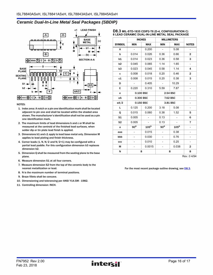
Ceramic Dual-In-Line Metal Seal Packages (SBDIP)
NOTES:
1. Index area: A notch or a pin one identification mark shall be located adjacent to pin one and shall be located within the shaded area shown. The manufacturer’s identification shall not be used as a pin one identification mark.
2. The maximum limits of lead dimensions b and c or M shall be measured at the centroid of the finished lead surfaces, when solder dip or tin plate lead finish is applied.
3. Dimensions b1 and c1 apply to lead base metal only. Dimension M applies to lead plating and finish thickness.
4. Corner leads (1, N, N/2 and N/2+1) may be configured with a partial lead paddle. For this configuration dimension b3 replaces dimension b2.
5. Dimension Q shall be measured from the seating plane to the base plane.
6. Measure dimension S1 at all four corners.
7. Measure dimension S2 from the top of the ceramic body to the nearest metallization or lead.
8. N is the maximum number of terminal positions.
9. Braze fillets shall be concave.
10. Dimensioning and tolerancing per ANSI Y14.5M - 1982.
11. Controlling dimension: INCH.
bbb C A - BS
c
Q
L
ASEATING
BASE
D
PLANE
PLANE
S S
-D--A-
-C-
eA
-B-
aaa C A - BM DS Sccc C A - BM DS S
D
E
S1
b2
b
A
e
M
c1
b1
(c)
(b)
SECTION A-A
BASE
LEAD FINISH
METAL
eA/2
S2
M
A
D8.3 MIL-STD-1835 CDIP2-T8 (D-4, CONFIGURATION C)8 LEAD CERAMIC DUAL-IN-LINE METAL SEAL PACKAGE
SYMBOL
INCHES MILLIMETERS
NOTESMIN MAX MIN MAX
A - 0.200 - 5.08 -
b 0.014 0.026 0.36 0.66 2
b1 0.014 0.023 0.36 0.58 3
b2 0.045 0.065 1.14 1.65 -
b3 0.023 0.045 0.58 1.14 4
c 0.008 0.018 0.20 0.46 2
c1 0.008 0.015 0.20 0.38 3
D - 0.405 - 10.29 -
E 0.220 0.310 5.59 7.87 -
e 0.100 BSC 2.54 BSC -
eA 0.300 BSC 7.62 BSC -
eA/2 0.150 BSC 3.81 BSC -
L 0.125 0.200 3.18 5.08 -
Q 0.015 0.060 0.38 1.52 5
S1 0.005 - 0.13 - 6
S2 0.005 - 0.13 - 7
a 90o 105o 90o 105o -
aaa - 0.015 - 0.38 -
bbb - 0.030 - 0.76 -
ccc - 0.010 - 0.25 -
M - 0.0015 - 0.038 2
N 8 8 8
Rev. 0 4/94
For the most recent package outline drawing, see D8.3.

http://www.renesas.comRefer to "http://www.renesas.com/" for the latest and detailed information.
Renesas Electronics America Inc.1001 Murphy Ranch Road, Milpitas, CA 95035, U.S.A.Tel: +1-408-432-8888, Fax: +1-408-434-5351Renesas Electronics Canada Limited9251 Yonge Street, Suite 8309 Richmond Hill, Ontario Canada L4C 9T3Tel: +1-905-237-2004Renesas Electronics Europe LimitedDukes Meadow, Millboard Road, Bourne End, Buckinghamshire, SL8 5FH, U.KTel: +44-1628-651-700, Fax: +44-1628-651-804Renesas Electronics Europe GmbHArcadiastrasse 10, 40472 Düsseldorf, Germany Tel: +49-211-6503-0, Fax: +49-211-6503-1327Renesas Electronics (China) Co., Ltd.Room 1709 Quantum Plaza, No.27 ZhichunLu, Haidian District, Beijing, 100191 P. R. ChinaTel: +86-10-8235-1155, Fax: +86-10-8235-7679Renesas Electronics (Shanghai) Co., Ltd.Unit 301, Tower A, Central Towers, 555 Langao Road, Putuo District, Shanghai, 200333 P. R. China Tel: +86-21-2226-0888, Fax: +86-21-2226-0999Renesas Electronics Hong Kong LimitedUnit 1601-1611, 16/F., Tower 2, Grand Century Place, 193 Prince Edward Road West, Mongkok, Kowloon, Hong KongTel: +852-2265-6688, Fax: +852 2886-9022Renesas Electronics Taiwan Co., Ltd.13F, No. 363, Fu Shing North Road, Taipei 10543, TaiwanTel: +886-2-8175-9600, Fax: +886 2-8175-9670Renesas Electronics Singapore Pte. Ltd.80 Bendemeer Road, Unit #06-02 Hyflux Innovation Centre, Singapore 339949Tel: +65-6213-0200, Fax: +65-6213-0300Renesas Electronics Malaysia Sdn.Bhd.Unit 1207, Block B, Menara Amcorp, Amcorp Trade Centre, No. 18, Jln Persiaran Barat, 46050 Petaling Jaya, Selangor Darul Ehsan, MalaysiaTel: +60-3-7955-9390, Fax: +60-3-7955-9510Renesas Electronics India Pvt. Ltd.No.777C, 100 Feet Road, HAL 2nd Stage, Indiranagar, Bangalore 560 038, IndiaTel: +91-80-67208700, Fax: +91-80-67208777Renesas Electronics Korea Co., Ltd.17F, KAMCO Yangjae Tower, 262, Gangnam-daero, Gangnam-gu, Seoul, 06265 KoreaTel: +82-2-558-3737, Fax: +82-2-558-5338
SALES OFFICES
© 2018 Renesas Electronics Corporation. All rights reserved.Colophon 7.0
(Rev.4.0-1 November 2017)
Notice
1. Descriptions of circuits, software and other related information in this document are provided only to illustrate the operation of semiconductor products and application examples. You are fully responsible for
the incorporation or any other use of the circuits, software, and information in the design of your product or system. Renesas Electronics disclaims any and all liability for any losses and damages incurred by
you or third parties arising from the use of these circuits, software, or information.
2. Renesas Electronics hereby expressly disclaims any warranties against and liability for infringement or any other claims involving patents, copyrights, or other intellectual property rights of third parties, by or
arising from the use of Renesas Electronics products or technical information described in this document, including but not limited to, the product data, drawings, charts, programs, algorithms, and application
examples.
3. No license, express, implied or otherwise, is granted hereby under any patents, copyrights or other intellectual property rights of Renesas Electronics or others.
4. You shall not alter, modify, copy, or reverse engineer any Renesas Electronics product, whether in whole or in part. Renesas Electronics disclaims any and all liability for any losses or damages incurred by
you or third parties arising from such alteration, modification, copying or reverse engineering.
5. Renesas Electronics products are classified according to the following two quality grades: “Standard” and “High Quality”. The intended applications for each Renesas Electronics product depends on the
product’s quality grade, as indicated below.
"Standard": Computers; office equipment; communications equipment; test and measurement equipment; audio and visual equipment; home electronic appliances; machine tools; personal electronic
equipment; industrial robots; etc.
"High Quality": Transportation equipment (automobiles, trains, ships, etc.); traffic control (traffic lights); large-scale communication equipment; key financial terminal systems; safety control equipment; etc.
Unless expressly designated as a high reliability product or a product for harsh environments in a Renesas Electronics data sheet or other Renesas Electronics document, Renesas Electronics products are
not intended or authorized for use in products or systems that may pose a direct threat to human life or bodily injury (artificial life support devices or systems; surgical implantations; etc.), or may cause
serious property damage (space system; undersea repeaters; nuclear power control systems; aircraft control systems; key plant systems; military equipment; etc.). Renesas Electronics disclaims any and all
liability for any damages or losses incurred by you or any third parties arising from the use of any Renesas Electronics product that is inconsistent with any Renesas Electronics data sheet, user’s manual or
other Renesas Electronics document.
6. When using Renesas Electronics products, refer to the latest product information (data sheets, user’s manuals, application notes, “General Notes for Handling and Using Semiconductor Devices” in the
reliability handbook, etc.), and ensure that usage conditions are within the ranges specified by Renesas Electronics with respect to maximum ratings, operating power supply voltage range, heat dissipation
characteristics, installation, etc. Renesas Electronics disclaims any and all liability for any malfunctions, failure or accident arising out of the use of Renesas Electronics products outside of such specified
ranges.
7. Although Renesas Electronics endeavors to improve the quality and reliability of Renesas Electronics products, semiconductor products have specific characteristics, such as the occurrence of failure at a
certain rate and malfunctions under certain use conditions. Unless designated as a high reliability product or a product for harsh environments in a Renesas Electronics data sheet or other Renesas
Electronics document, Renesas Electronics products are not subject to radiation resistance design. You are responsible for implementing safety measures to guard against the possibility of bodily injury, injury
or damage caused by fire, and/or danger to the public in the event of a failure or malfunction of Renesas Electronics products, such as safety design for hardware and software, including but not limited to
redundancy, fire control and malfunction prevention, appropriate treatment for aging degradation or any other appropriate measures. Because the evaluation of microcomputer software alone is very difficult
and impractical, you are responsible for evaluating the safety of the final products or systems manufactured by you.
8. Please contact a Renesas Electronics sales office for details as to environmental matters such as the environmental compatibility of each Renesas Electronics product. You are responsible for carefully and
sufficiently investigating applicable laws and regulations that regulate the inclusion or use of controlled substances, including without limitation, the EU RoHS Directive, and using Renesas Electronics
products in compliance with all these applicable laws and regulations. Renesas Electronics disclaims any and all liability for damages or losses occurring as a result of your noncompliance with applicable
laws and regulations.
9. Renesas Electronics products and technologies shall not be used for or incorporated into any products or systems whose manufacture, use, or sale is prohibited under any applicable domestic or foreign laws
or regulations. You shall comply with any applicable export control laws and regulations promulgated and administered by the governments of any countries asserting jurisdiction over the parties or
transactions.
10. It is the responsibility of the buyer or distributor of Renesas Electronics products, or any other party who distributes, disposes of, or otherwise sells or transfers the product to a third party, to notify such third
party in advance of the contents and conditions set forth in this document.
11. This document shall not be reprinted, reproduced or duplicated in any form, in whole or in part, without prior written consent of Renesas Electronics.
12. Please contact a Renesas Electronics sales office if you have any questions regarding the information contained in this document or Renesas Electronics products.
(Note 1) “Renesas Electronics” as used in this document means Renesas Electronics Corporation and also includes its directly or indirectly controlled subsidiaries.
(Note 2) “Renesas Electronics product(s)” means any product developed or manufactured by or for Renesas Electronics.