investigation of spin-on dielectrics as an interlayer ... · investigation of spin-on dielectrics...
TRANSCRIPT
Investigation of Spin-on Dielectrics as an Interlayer Dielectric for the
Marvell Nanofabrication Laboratory CMOS210 Baseline Project
Kevin Crabbe and Jeffrey Clarkson
Contact Information [email protected], (925)-451-8596
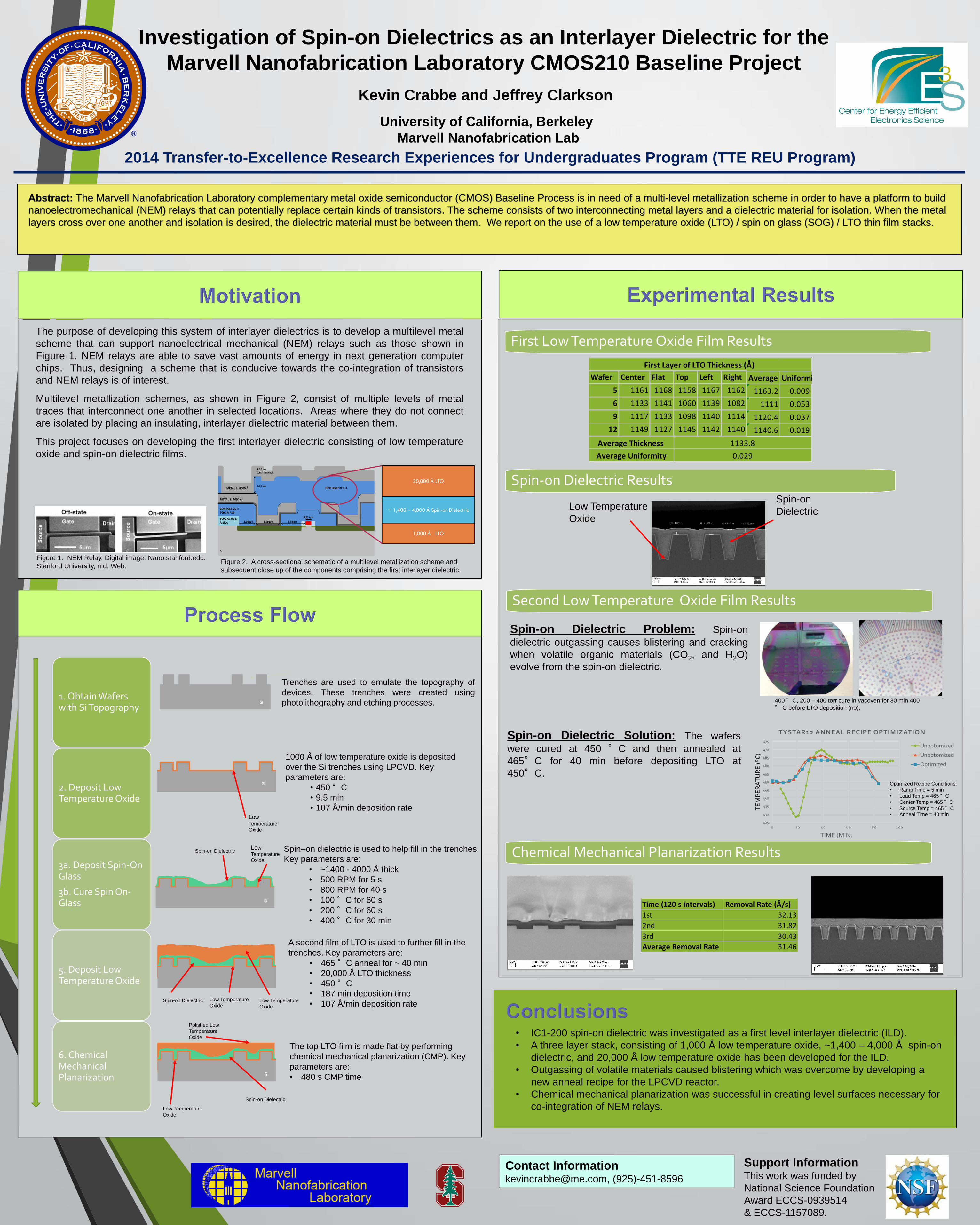
The purpose of developing this system of interlayer dielectrics is to develop a multilevel metal
scheme that can support nanoelectrical mechanical (NEM) relays such as those shown in
Figure 1. NEM relays are able to save vast amounts of energy in next generation computer
chips. Thus, designing a scheme that is conducive towards the co-integration of transistors
and NEM relays is of interest.
Multilevel metallization schemes, as shown in Figure 2, consist of multiple levels of metal
traces that interconnect one another in selected locations. Areas where they do not connect
are isolated by placing an insulating, interlayer dielectric material between them.
This project focuses on developing the first interlayer dielectric consisting of low temperature
oxide and spin-on dielectric films.
Support Information This work was funded by
National Science Foundation
Award ECCS-0939514
& ECCS-1157089.
Abstract: The Marvell Nanofabrication Laboratory complementary metal oxide semiconductor (CMOS) Baseline Process is in need of a multi-level metallization scheme in order to have a platform to build
nanoelectromechanical (NEM) relays that can potentially replace certain kinds of transistors. The scheme consists of two interconnecting metal layers and a dielectric material for isolation. When the metal
layers cross over one another and isolation is desired, the dielectric material must be between them. We report on the use of a low temperature oxide (LTO) / spin on glass (SOG) / LTO thin film stacks.
2014 Transfer-to-Excellence Research Experiences for Undergraduates Program (TTE REU Program)
University of California, Berkeley
Marvell Nanofabrication Lab
1. Obtain Wafers with Si Topography
2. Deposit Low Temperature Oxide
3a. Deposit Spin-On Glass
3b. Cure Spin On-Glass
5. Deposit Low Temperature Oxide
6. Chemical Mechanical Planarization
1000 Å of low temperature oxide is deposited
over the Si trenches using LPCVD. Key
parameters are:
• 450 °C
• 9.5 min
• 107 Å/min deposition rate
Spin–on dielectric is used to help fill in the trenches.
Key parameters are:
• ~1400 - 4000 Å thick
• 500 RPM for 5 s
• 800 RPM for 40 s
• 100 °C for 60 s
• 200 °C for 60 s
• 400 °C for 30 min
The top LTO film is made flat by performing
chemical mechanical planarization (CMP). Key
parameters are:
• 480 s CMP time
Figure 1. NEM Relay. Digital image. Nano.stanford.edu.
Stanford University, n.d. Web.
Trenches are used to emulate the topography of
devices. These trenches were created using
photolithography and etching processes.
A second film of LTO is used to further fill in the
trenches. Key parameters are:
• 465 °C anneal for ~ 40 min
• 20,000 Å LTO thickness
• 450 °C
• 187 min deposition time
• 107 Å/min deposition rate
• IC1-200 spin-on dielectric was investigated as a first level interlayer dielectric (ILD).
• A three layer stack, consisting of 1,000 Å low temperature oxide, ~1,400 – 4,000 Å spin-on
dielectric, and 20,000 Å low temperature oxide has been developed for the ILD.
• Outgassing of volatile materials caused blistering which was overcome by developing a
new anneal recipe for the LPCVD reactor.
• Chemical mechanical planarization was successful in creating level surfaces necessary for
co-integration of NEM relays.
Wafer Center Flat Top Left Right Average Uniformity
5 1161 1168 1158 1167 1162 1163.2 0.009
6 1133 1141 1060 1139 1082 1111 0.053
9 1117 1133 1098 1140 1114 1120.4 0.037
12 1149 1127 1145 1142 1140 1140.6 0.019
First Layer of LTO Thickness (Å)
Average Uniformity
Average Thickness 1133.8
0.029
Spin-on
Dielectric Low Temperature
Oxide
Spin-on Dielectric Problem: Spin-on
dielectric outgassing causes blistering and cracking
when volatile organic materials (CO2, and H2O)
evolve from the spin-on dielectric.
425
430
435
440
445
450
455
460
465
470
475
0 2 0 4 0 6 0 8 0 1 0 0
TE
MP
ER
AT
UR
E (
°C)
TIME (MIN)
TYSTAR12 ANNEAL RECIPE OPTIMIZATION
Unoptomized
Unoptomized
Optimized
Optimized Recipe Conditions:
• Ramp Time = 5 min
• Load Temp = 465 °C
• Center Temp = 465 °C
• Source Temp = 465 °C
• Anneal Time = 40 min
400 °C, 200 – 400 torr cure in vacoven for 30 min 400
° C before LTO deposition (no).
. Low
Temperature
Oxide
Spin-on Dielectric
Spin-on Dielectric Low Temperature
Oxide Low Temperature
Oxide
Polished Low
Temperature
Oxide
Spin-on Dielectric
Low Temperature
Oxide
Time (120 s intervals) Removal Rate (Å/s)
1st 32.13
2nd 31.82
3rd 30.43
Average Removal Rate 31.46
Figure 2. A cross-sectional schematic of a multilevel metallization scheme and
subsequent close up of the components comprising the first interlayer dielectric.
Low
Temperature
Oxide
First Low Temperature Oxide Film Results
Spin-on Dielectric Results
Second Low Temperature Oxide Film Results
Spin-on Dielectric Solution: The wafers
were cured at 450 °C and then annealed at
465°C for 40 min before depositing LTO at
450°C.
Chemical Mechanical Planarization Results