introduction and the architecture of fpga -...
TRANSCRIPT
© 2011 Altera Corporation—Confidential
Introduction and the architecture of FPGA Introduction and the architecture of FPGA
© 2011 Altera Corporation—Confidential2
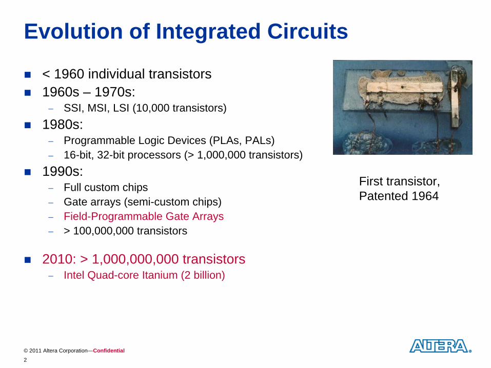
Evolution of Integrated Circuits
< 1960 individual transistors
1960s – 1970s:
SSI, MSI, LSI (10,000 transistors)
1980s:
Programmable Logic Devices (PLAs, PALs)
16-bit, 32-bit processors (> 1,000,000 transistors)
1990s:
Full custom chips
Gate arrays (semi-custom chips)
Field-Programmable Gate Arrays
> 100,000,000 transistors
2010: > 1,000,000,000 transistors
Intel Quad-core Itanium (2 billion)
First transistor,Patented 1964
© 2011 Altera Corporation—Confidential3
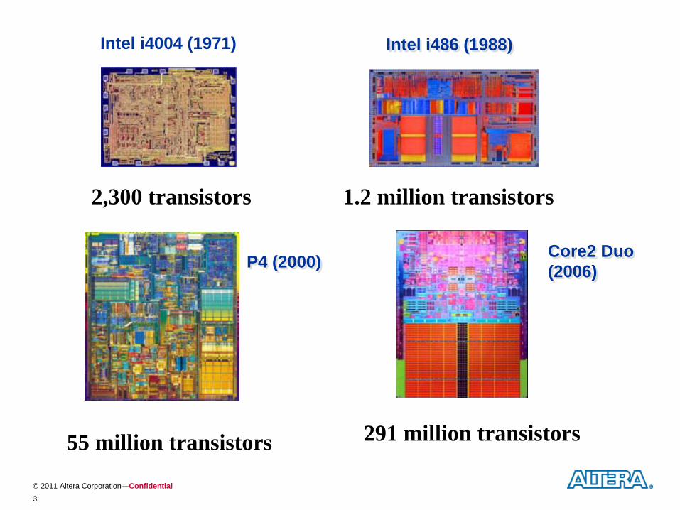
Intel i4004 (1971)
2,300 transistors
Intel i486 (1988)Intel i486 (1988)
1.2 million transistors
P4 (2000)P4 (2000)
55 million transistors 291 million transistors
Core2 Duo (2006) Core2 Duo (2006)
© 2011 Altera Corporation—Confidential4
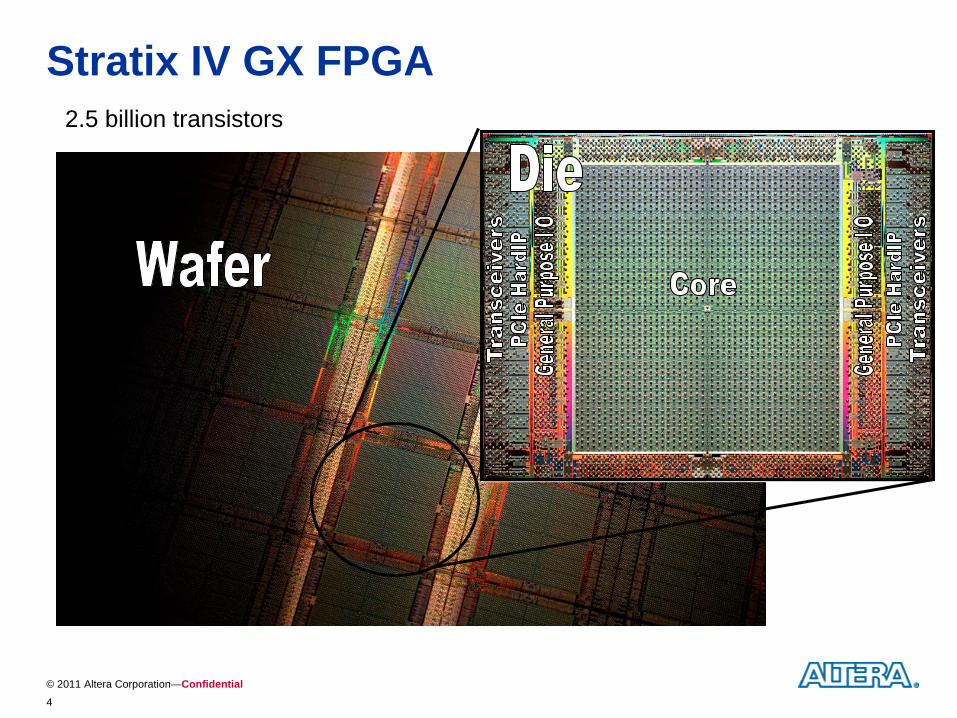
Stratix IV GX FPGA2.5 billion transistors
© 2011 Altera Corporation—Confidential5
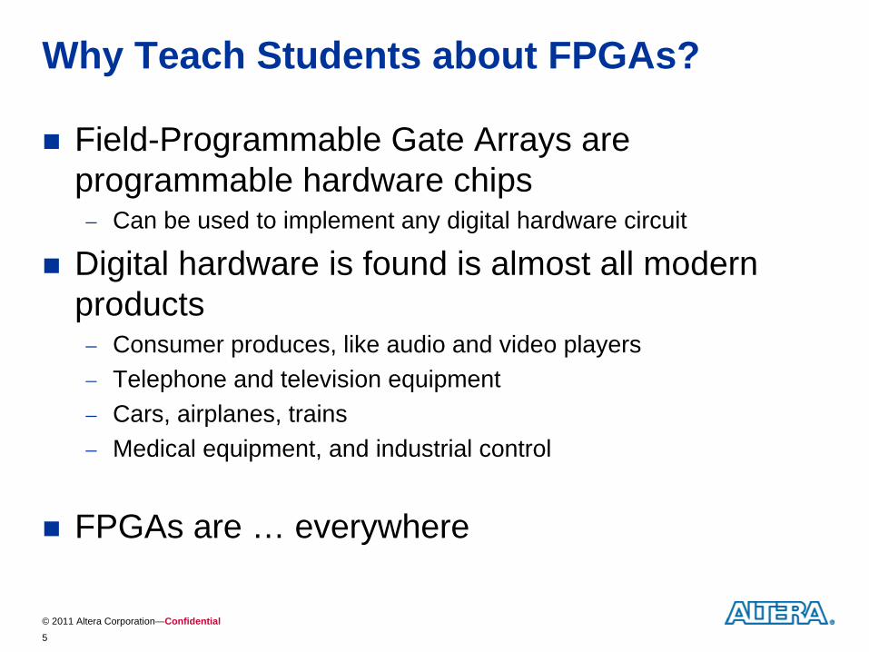
Why Teach Students about FPGAs?
Field-Programmable Gate Arrays are programmable hardware chips
Can be used to implement any digital hardware circuit
Digital hardware is found is almost all modern products
Consumer produces, like audio and video players
Telephone and television equipment
Cars, airplanes, trains
Medical equipment, and industrial control
FPGAs are … everywhere
© 2011 Altera Corporation—Confidential6
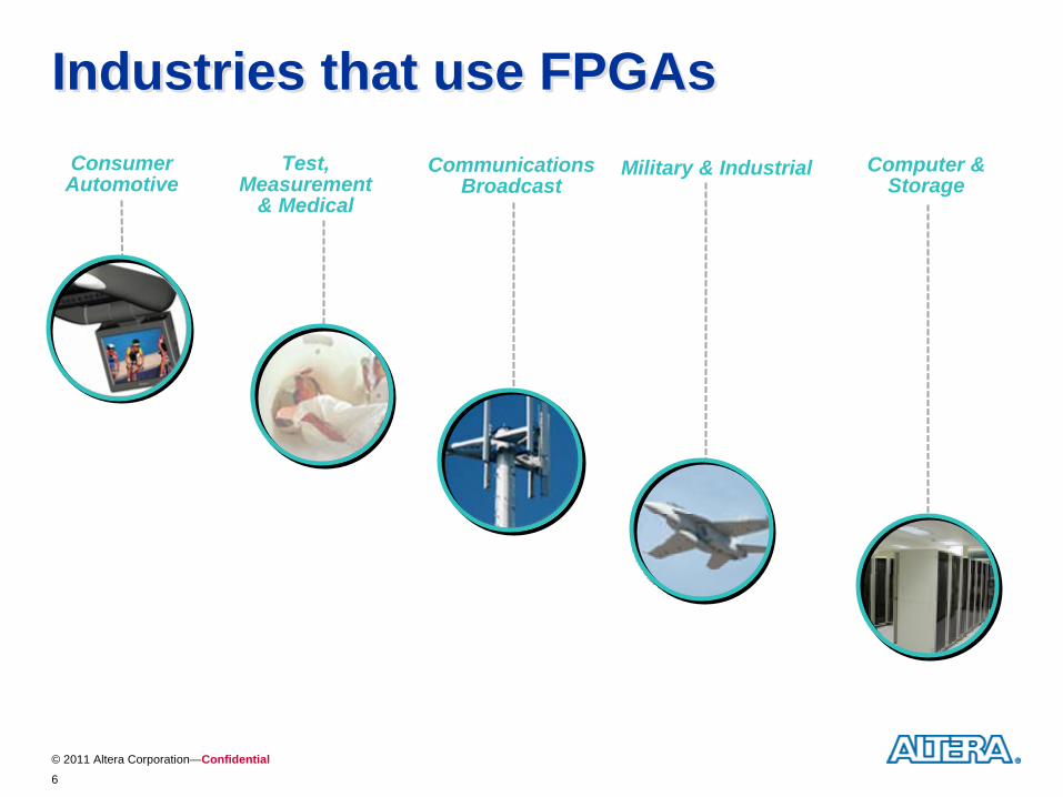
Industries that use FPGAsIndustries that use FPGAsCommunications
BroadcastConsumerAutomotive
Test, Measurement
& Medical
Computer & Storage
Military & Industrial
© 2011 Altera Corporation—Confidential7
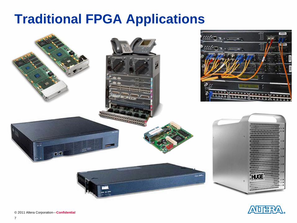
Traditional FPGA Applications
© 2011 Altera Corporation—Confidential8
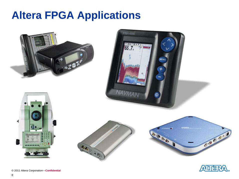
Altera FPGA Applications

© 2011 Altera Corporation—Confidential9
Consumer Applications
Set-Top Boxes
LCD, Plasma Displays/TVs Camcorders
Printers
Touch Panels
DVD Players
Handheld Media Players
Consumer Music
© 2011 Altera Corporation—Confidential
What are FPGAs and why should we use them? What are FPGAs and why should we use them?
© 2011 Altera Corporation—Confidential11
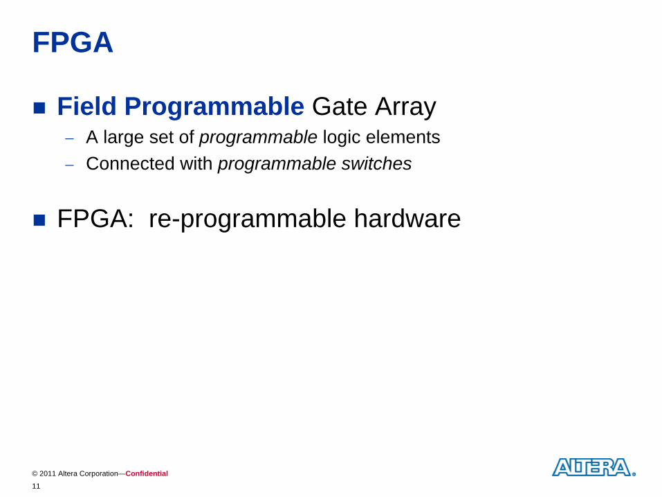
FPGA
Field Programmable Gate Array
A large set of programmable logic elements
Connected with programmable switches
FPGA: re-programmable hardware
© 2011 Altera Corporation—Confidential12
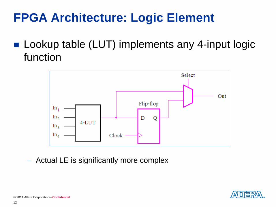
FPGA Architecture: Logic Element
Lookup table (LUT) implements any 4-input logic function
Actual LE is significantly more complex
© 2011 Altera Corporation—Confidential13
…
…
… … … … … …
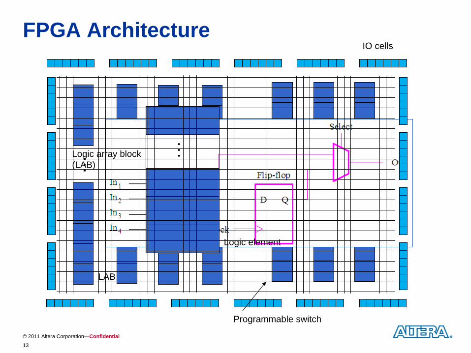
FPGA Architecture
Logic element
LAB…
Logic array block (LAB)
IO cells
Programmable switch
© 2011 Altera Corporation—Confidential14
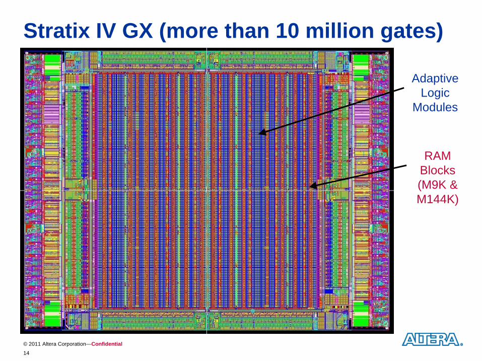
Stratix IV GX (more than 10 million gates)
Adaptive Logic
Modules
RAM Blocks (M9K & M144K)
© 2011 Altera Corporation—Confidential15
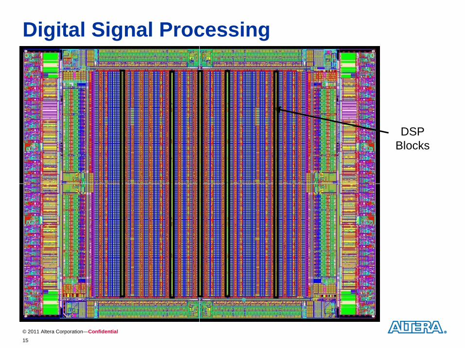
Digital Signal Processing
DSP Blocks
© 2011 Altera Corporation—Confidential16
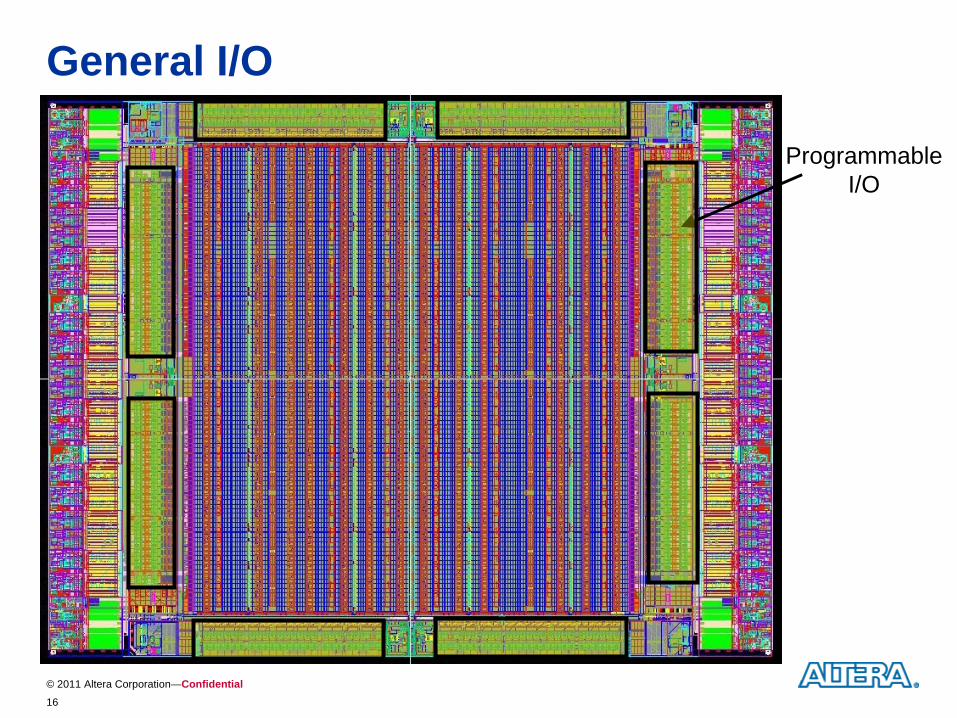
General I/O
Programmable I/O
© 2011 Altera Corporation—Confidential17
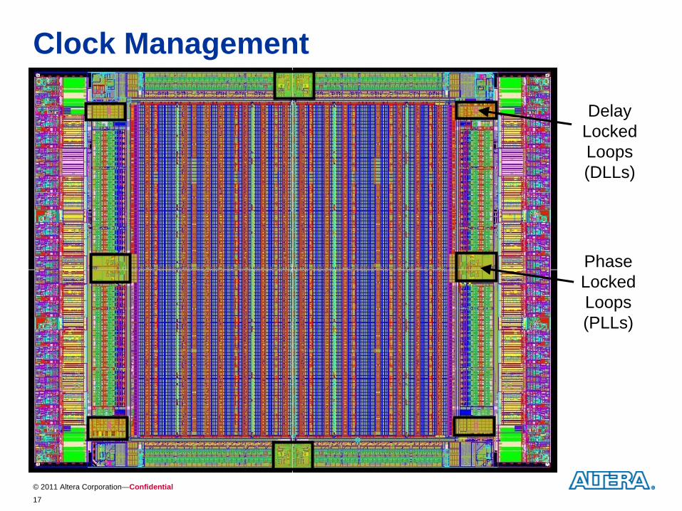
Clock Management
Delay Locked Loops (DLLs)
Phase Locked Loops (PLLs)
© 2011 Altera Corporation—Confidential18
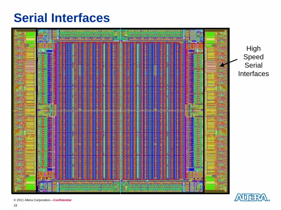
Serial Interfaces
High Speed Serial
Interfaces
© 2011 Altera Corporation—Confidential
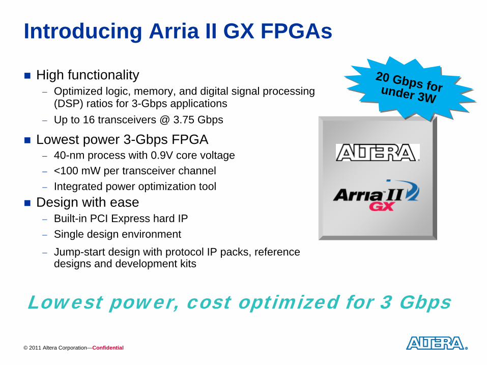
Introducing Arria II GX FPGAs
High functionality
Optimized logic, memory, and digital signal processing (DSP) ratios for 3-Gbps applications
Up to 16 transceivers @ 3.75 Gbps
Lowest power 3-Gbps FPGA
40-nm process with 0.9V core voltage
<100 mW per transceiver channel
Integrated power optimization tool
Design with ease
Built-in PCI Express hard IP
Single design environment
Jump-start design with protocol IP packs, reference designs and development kits
Lowest power, cost optimized for 3 Gbps
20 Gbps for under 3W
20 Gbps for under 3W
© 2011 Altera Corporation—Confidential
20
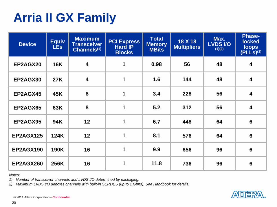
Arria II GX Family
Device Equiv LEs
Maximum Transceiver Channels(1)
PCI Express Hard IP Blocks
Total Memory MBits
18 X 18 Multipliers
Max. LVDS I/O
(1)(2)
Phase- locked loops
(PLLs)(1)
EP2AGX20 16K 4 1 0.98 56 48 4
EP2AGX30 27K 4 1 1.6 144 48 4
EP2AGX45 45K 8 1 3.4 228 56 4
EP2AGX65 63K 8 1 5.2 312 56 4
EP2AGX95 94K 12 1 6.7 448 64 6
EP2AGX125 124K 12 1 8.1 576 64 6
EP2AGX190 190K 16 1 9.9 656 96 6
EP2AGX260 256K 16 1 11.8 736 96 6
Notes:1) Number of transceiver channels and LVDS I/O determined by packaging.2) Maximum LVDS I/O denotes channels with built-in SERDES (up to 1 Gbps). See Handbook for details.
© 2011 Altera Corporation—Confidential
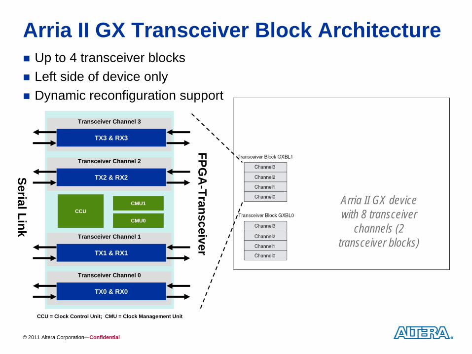
Arria II GX Transceiver Block Architecture
Up to 4 transceiver blocks
Left side of device only
Dynamic reconfiguration support
Arria II GX device with 8 transceiver
channels (2 transceiver blocks)
FPGA
-Transceiver
CCUCMU1
CMU0
Transceiver Channel 3
TX3 & RX3
Transceiver Channel 2
TX2 & RX2
Transceiver Channel 1
TX1 & RX1
Transceiver Channel 0
TX0 & RX0
Serial Link
CCU = Clock Control Unit; CMU = Clock Management Unit
© 2011 Altera Corporation—Confidential22
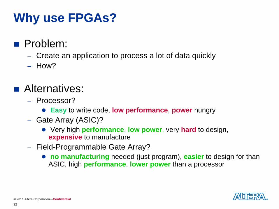
Why use FPGAs?
Problem:
Create an application to process a lot of data quickly
How?
Alternatives:
Processor?
Easy to write code, low performance, power hungry
Gate Array (ASIC)?
Very high performance, low power, very hard to design, expensive to manufacture
Field-Programmable Gate Array?
no manufacturing needed (just program), easier to design for than ASIC, high performance, lower power than a processor
© 2011 Altera Corporation—Confidential23
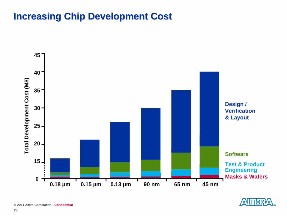
Increasing Chip Development CostIncreasing Chip Development CostTo
tal D
evel
opm
ent C
ost (
M$)
45
20
40
35
30
25
15
00.18 µm 0.15 µm 0.13 µm 90 nm 65 nm 45 nm
Masks & Wafers
Test & ProductEngineering
Software
Design /Verification& Layout
© 2011 Altera Corporation—Confidential24
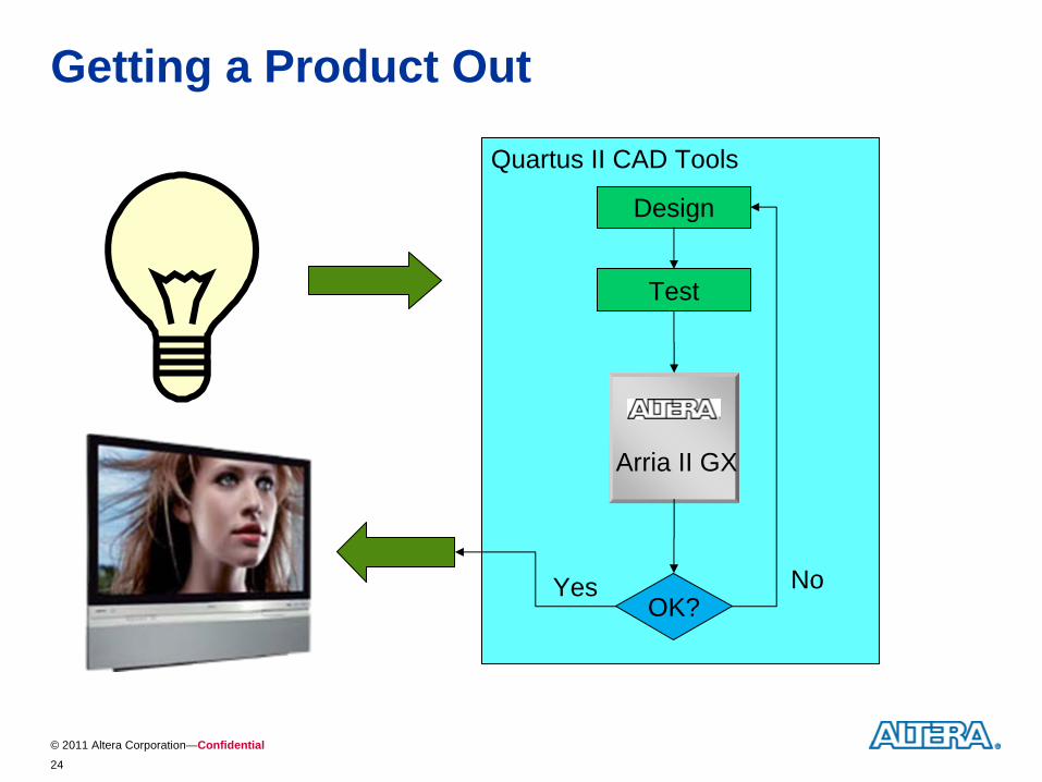
Quartus II CAD Tools
Getting a Product Out
Design
Test
OK?Yes No
Arria II GX
© 2011 Altera Corporation—Confidential25
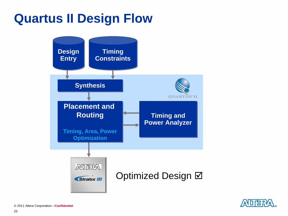
Quartus II Design Flow
DesignEntry
DesignEntry
TimingConstraints
TimingConstraints
SynthesisSynthesis
Placement and Routing
Timing, Area, PowerOptimization
Placement and Routing
Timing, Area, PowerOptimization
Timing and Power Analyzer
Timing and Power Analyzer
Optimized Design
© 2011 Altera Corporation—Confidential26
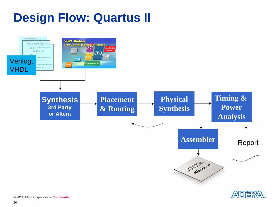
Design Flow: Quartus II
Synthesis3rd Partyor Altera
Placement& Routing
PhysicalSynthesis
Timing & Power
Analysis
// Begin: Write Controlalways @ (posedge wrbusy_int)begin
write0 <= 1'b1;write1 <= 1'b0;writex <= 1'b0;
end
always @ (negedge wrbusy_int)begin
write0 <= 1'b0;end
always @ (posedge write0_done)begin
write1 <= 1'b1;
// Begin: Write Controlalways @ (posedge wrbusy_int)begin
write0 <= 1'b1;write1 <= 1'b0;writex <= 1'b0;
end
always @ (negedge wrbusy_int)begin
write0 <= 1'b0;end
always @ (posedge write0_done)begin
write1 <= 1'b1;
// Begin: Write Controlalways @ (posedge wrbusy_int)begin
write0 <= 1'b1;write1 <= 1'b0;writex <= 1'b0;
end
always @ (negedge wrbusy_int)begin
write0 <= 1'b0;end
always @ (posedge write0_done)begin
write1 <= 1'b1;
Verilog,VHDL
ReportAssembler
© 2011 Altera Corporation—Confidential
Teaching with Altera CAD Tools and Educational Platform Teaching with Altera CAD Tools and Educational Platform
© 2011 Altera Corporation—Confidential28
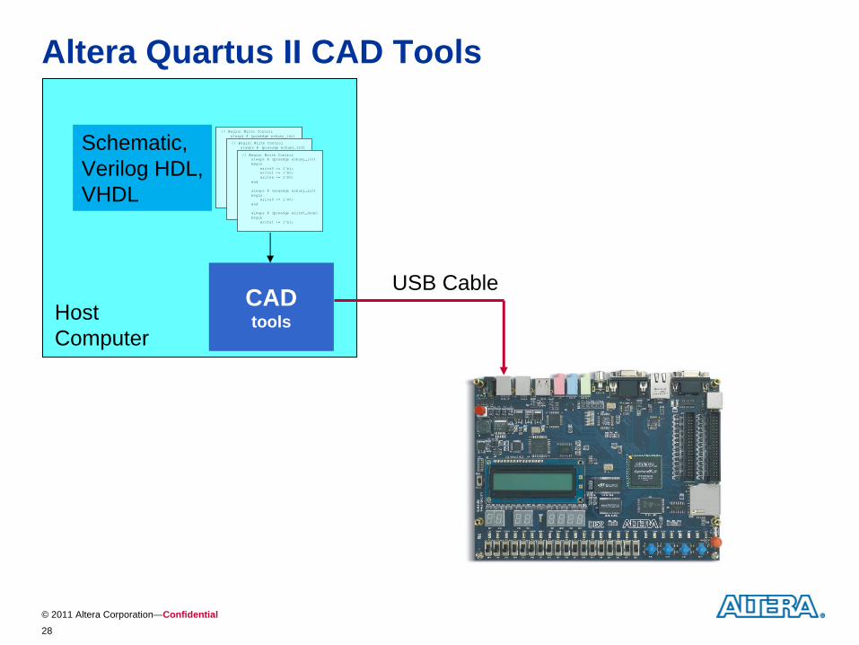
Altera Quartus II CAD Tools
CADtools
// Begin: Write Controlalways @ (posedge wrbusy_int)begin
write0 <= 1'b1;write1 <= 1'b0;writex <= 1'b0;
end
always @ (negedge wrbusy_int)begin
write0 <= 1'b0;end
always @ (posedge write0_done)begin
write1 <= 1'b1;
// Begin: Write Controlalways @ (posedge wrbusy_int)begin
write0 <= 1'b1;write1 <= 1'b0;writex <= 1'b0;
end
always @ (negedge wrbusy_int)begin
write0 <= 1'b0;end
always @ (posedge write0_done)begin
write1 <= 1'b1;
// Begin: Write Controlalways @ (posedge wrbusy_int)begin
write0 <= 1'b1;write1 <= 1'b0;writex <= 1'b0;
end
always @ (negedge wrbusy_int)begin
write0 <= 1'b0;end
always @ (posedge write0_done)begin
write1 <= 1'b1;
Schematic, Verilog HDL,VHDL
HostComputer
USB Cable
© 2011 Altera Corporation—Confidential29
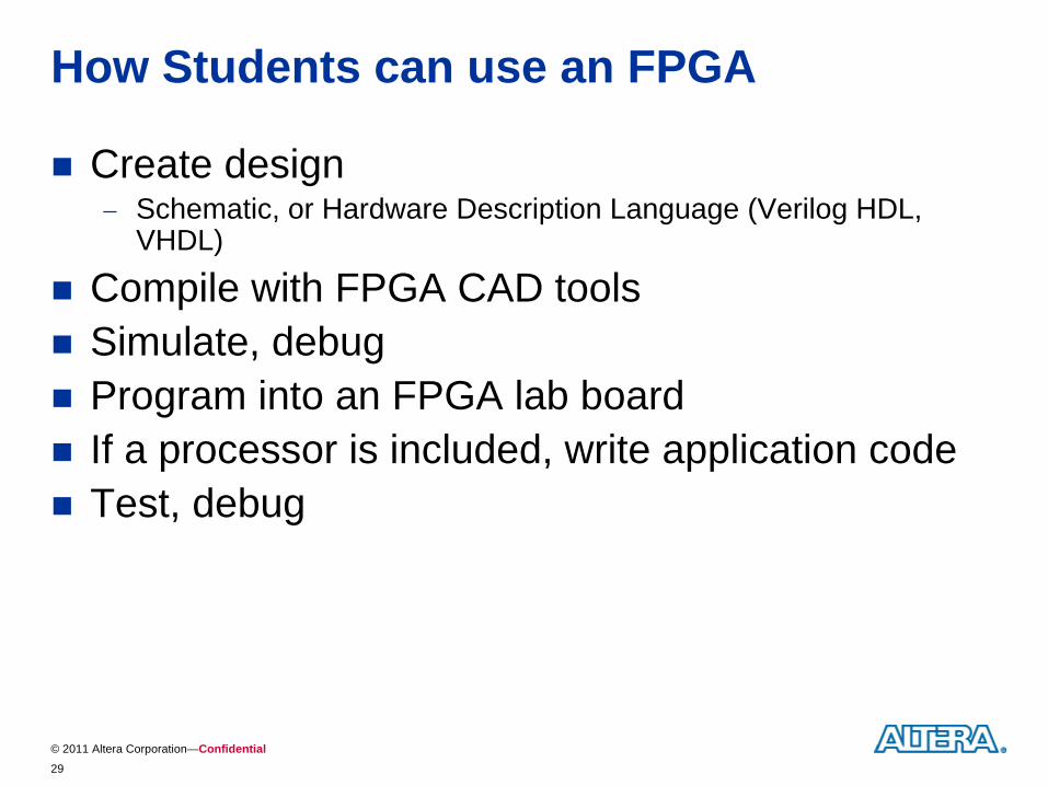
How Students can use an FPGA
Create design
Schematic, or Hardware Description Language (Verilog HDL, VHDL)
Compile with FPGA CAD tools
Simulate, debug
Program into an FPGA lab board
If a processor is included, write application code
Test, debug
© 2011 Altera Corporation—Confidential30
Teaching Materials Needed
FPGA lab board
with all the right pedagogical features
CAD tools – Quartus II
with tutorials to learn how to use the software
Lab experiments
that fit into a modern curriculum
that cover the fundamentals and are fun/challenging/interesting
© 2011 Altera Corporation—Confidential31
Developing Teaching Materials
Materials that help with teaching Digital Logic and Computer Organization
What is our approach?
Examine the material covered in a course
Create exercises that enhance student learning
Creative and Interesting examples
Progressive learning
Build knowledge base with easy examples first
Extend examples to allow students to enhance their understanding
Materials are designed for our Educational Boards (DE2/DE1)
© 2011 Altera Corporation—Confidential32
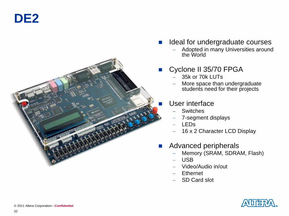
DE2
Ideal for undergraduate courses
Adopted in many Universities around the World
Cyclone II 35/70 FPGA
35k or 70k LUTs
More space than undergraduate students need for their projects
User interface
Switches
7-segment displays
LEDs
16 x 2 Character LCD Display
Advanced peripherals
Memory (SRAM, SDRAM, Flash)
USB
Video/Audio in/out
Ethernet
SD Card slot
© 2011 Altera Corporation—Confidential33
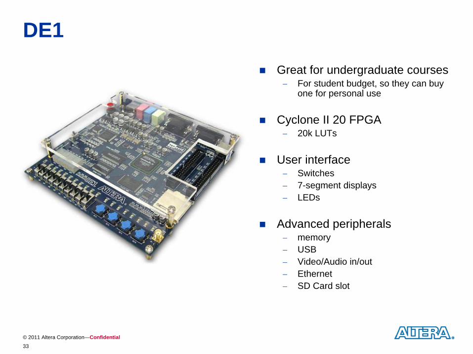
DE1
Great for undergraduate courses
For student budget, so they can buy one for personal use
Cyclone II 20 FPGA
20k LUTs
User interface
Switches
7-segment displays
LEDs
Advanced peripherals
memory
USB
Video/Audio in/out
Ethernet
SD Card slot
© 2011 Altera Corporation—Confidential
Digital Logic ExcecisesDigital Logic Excecises
© 2011 Altera Corporation—Confidential35
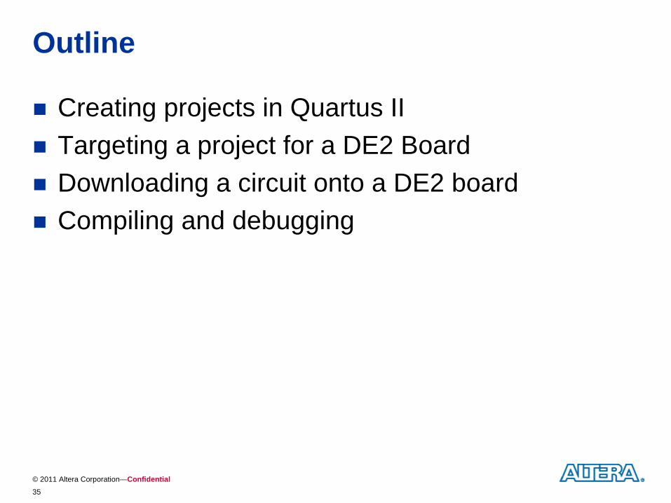
Outline
Creating projects in Quartus II
Targeting a project for a DE2 Board
Downloading a circuit onto a DE2 board
Compiling and debugging
© 2011 Altera Corporation—Confidential36
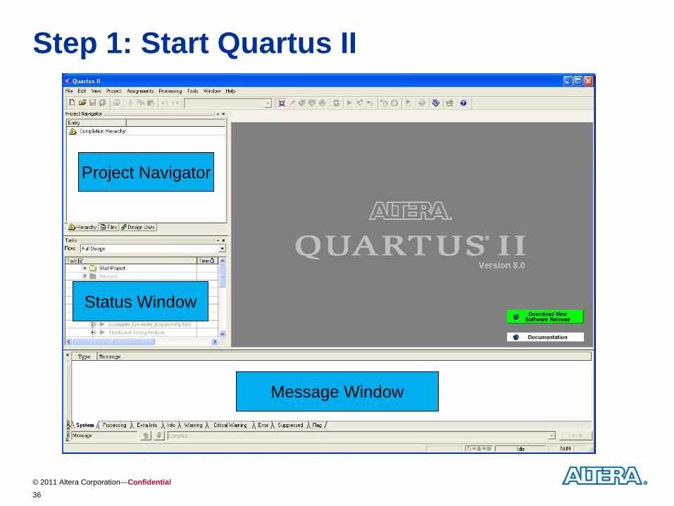
Step 1: Start Quartus II
Message Window
Project Navigator
Status Window
© 2011 Altera Corporation—Confidential37
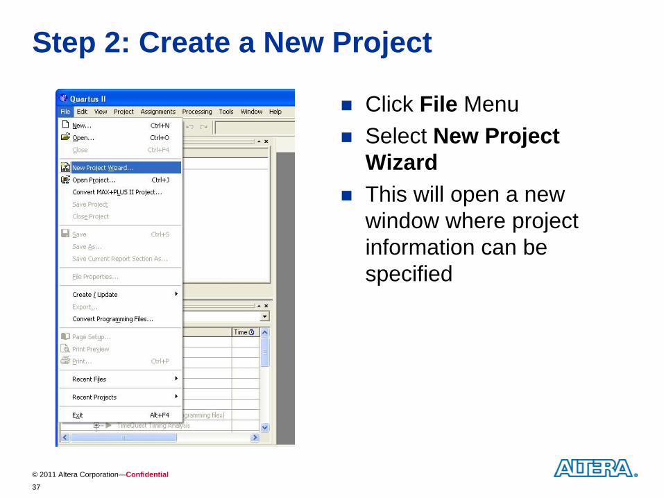
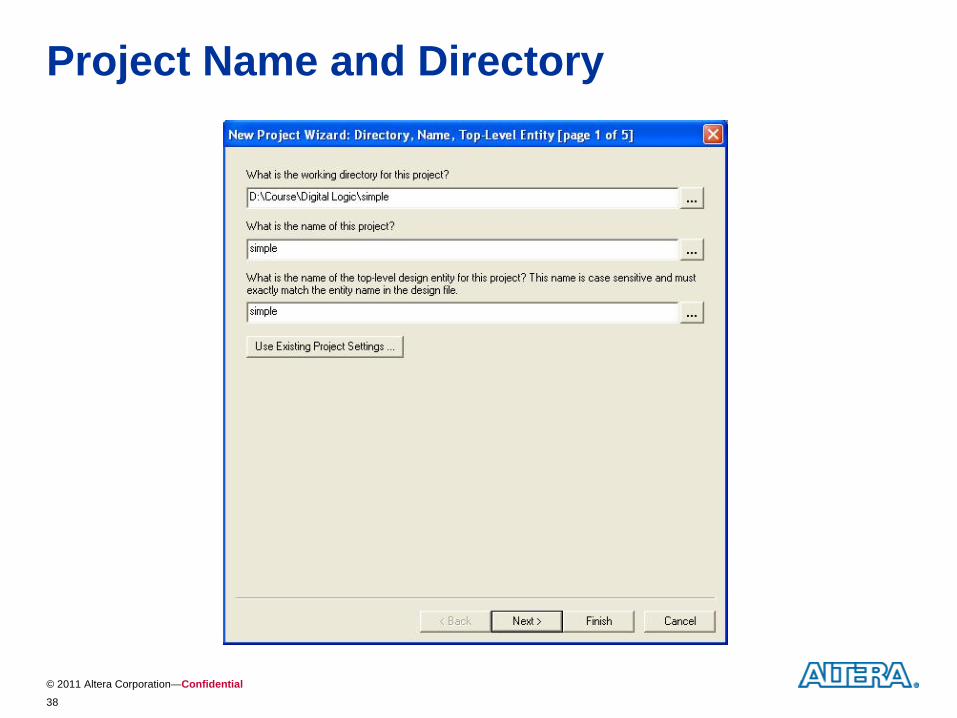
Step 2: Create a New Project
Click File Menu
Select New Project Wizard
This will open a new window where project information can be specified
© 2011 Altera Corporation—Confidential38
Project Name and Directory
© 2011 Altera Corporation—Confidential39
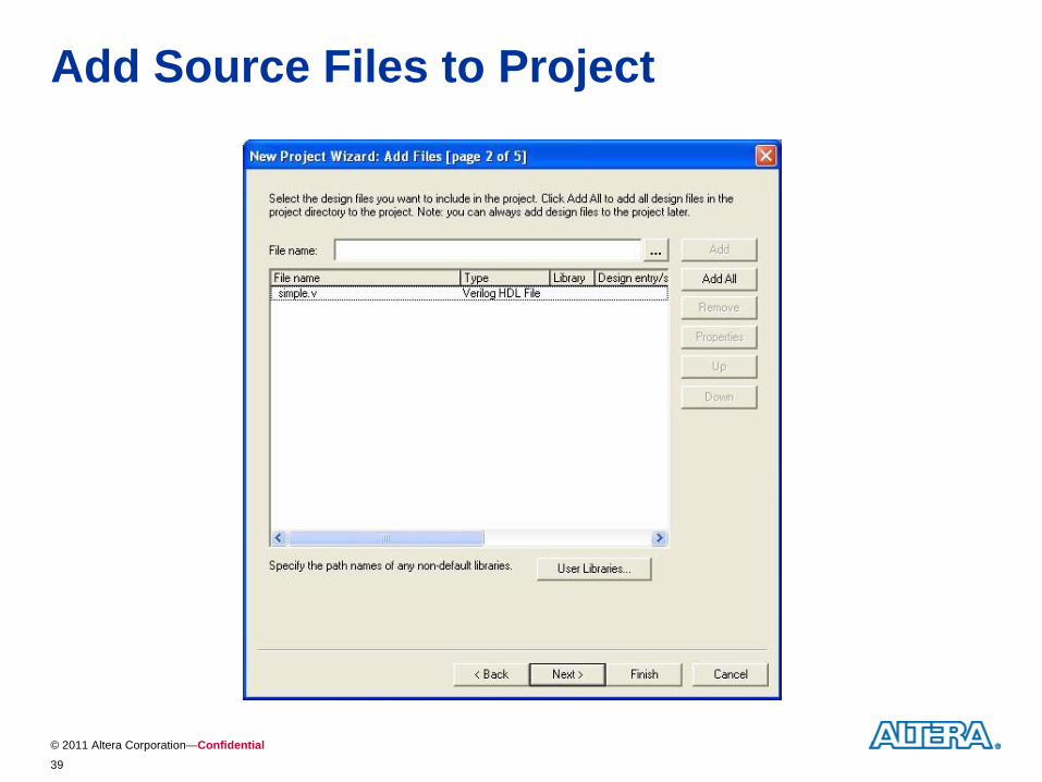
Add Source Files to Project
© 2011 Altera Corporation—Confidential40
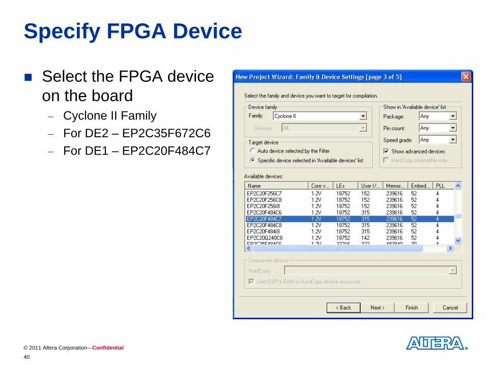
Specify FPGA Device
Select the FPGA device on the board
Cyclone II Family
For DE2 – EP2C35F672C6
For DE1 – EP2C20F484C7
© 2011 Altera Corporation—Confidential41
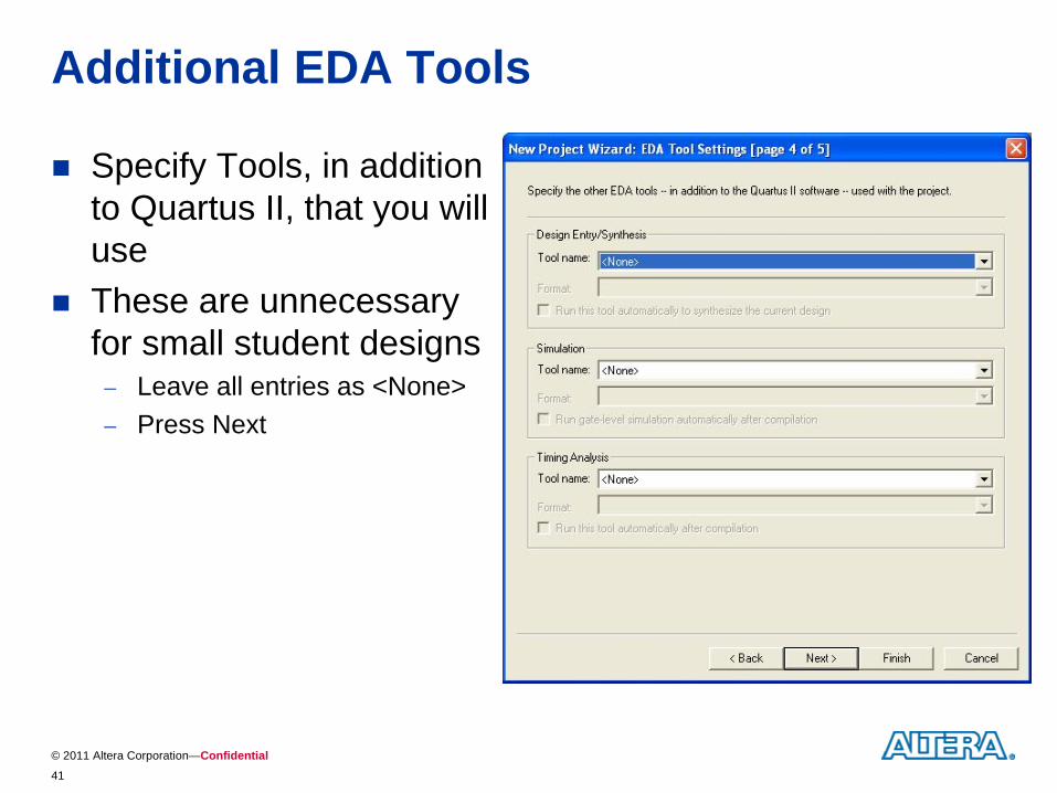
Additional EDA Tools
Specify Tools, in addition to Quartus II, that you will use
These are unnecessary for small student designs
Leave all entries as <None>
Press Next
© 2011 Altera Corporation—Confidential42
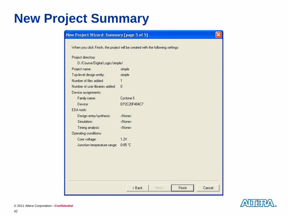
New Project Summary
© 2011 Altera Corporation—Confidential43
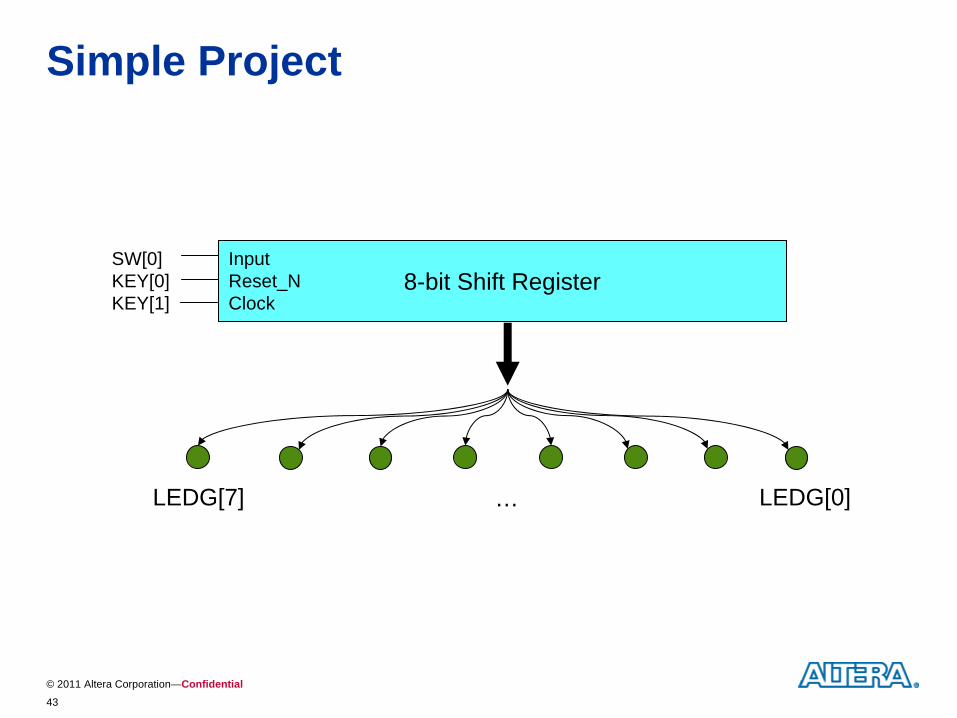
Simple Project
8-bit Shift RegisterInputReset_NClock
SW[0]KEY[0]KEY[1]
LEDG[7] … LEDG[0]
© 2011 Altera Corporation—Confidential44
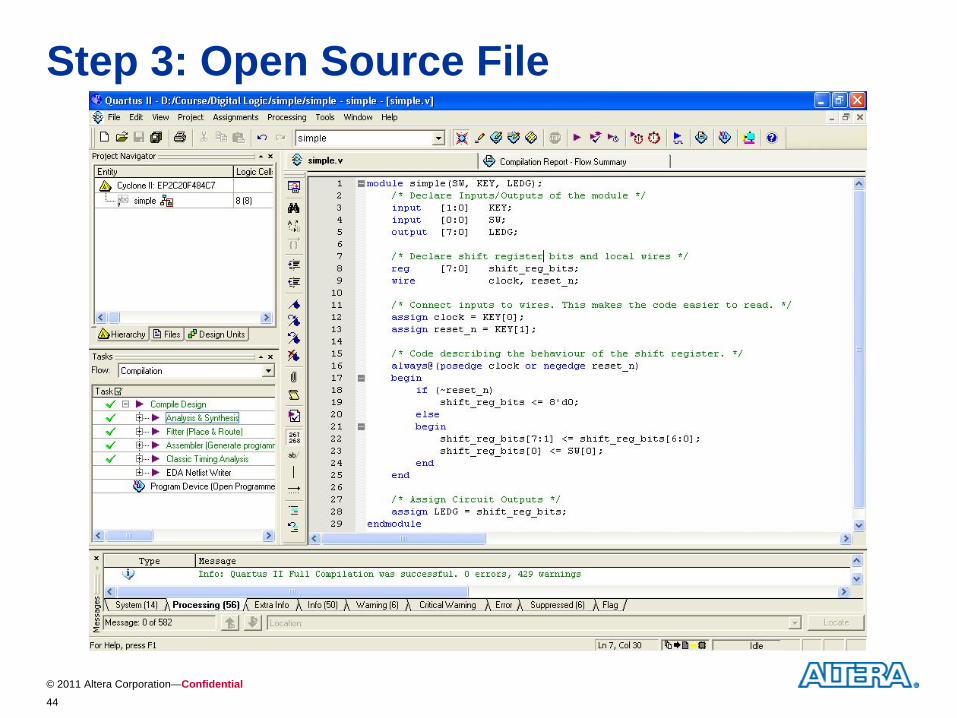
Step 3: Open Source File
© 2011 Altera Corporation—Confidential45
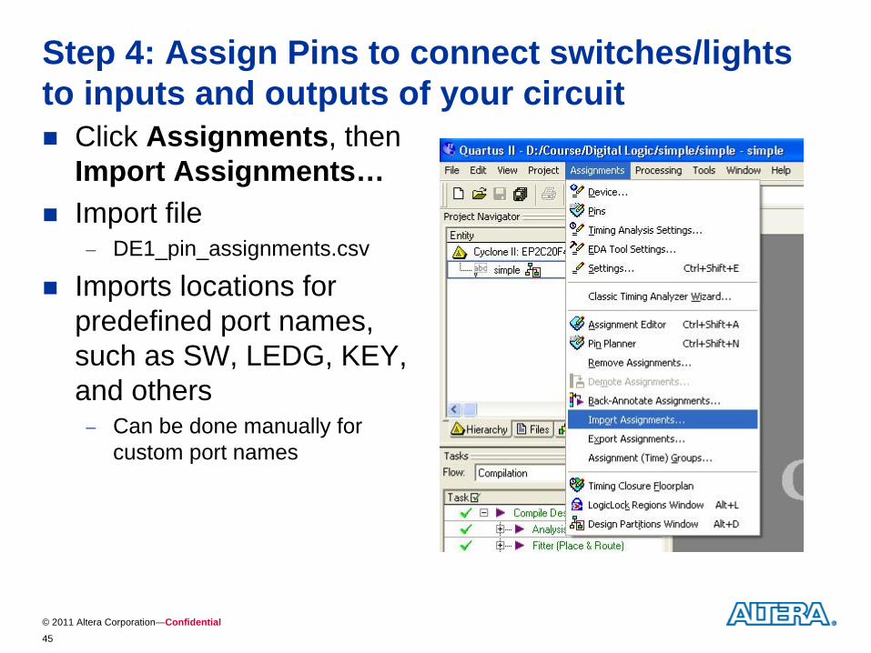
Step 4: Assign Pins to connect switches/lights to inputs and outputs of your circuit
Click Assignments, then Import Assignments…
Import file
DE1_pin_assignments.csv
Imports locations for predefined port names, such as SW, LEDG, KEY, and others
Can be done manually for custom port names
© 2011 Altera Corporation—Confidential46
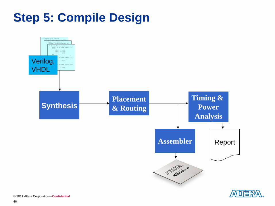
Step 5: Compile Design
SynthesisPlacement& Routing
Timing & Power
Analysis
// Begin: Write Controlalways @ (posedge wrbusy_int)begin
write0 <= 1'b1;write1 <= 1'b0;writex <= 1'b0;
end
always @ (negedge wrbusy_int)begin
write0 <= 1'b0;end
always @ (posedge write0_done)begin
write1 <= 1'b1;
// Begin: Write Controlalways @ (posedge wrbusy_int)begin
write0 <= 1'b1;write1 <= 1'b0;writex <= 1'b0;
end
always @ (negedge wrbusy_int)begin
write0 <= 1'b0;end
always @ (posedge write0_done)begin
write1 <= 1'b1;
// Begin: Write Controlalways @ (posedge wrbusy_int)begin
write0 <= 1'b1;write1 <= 1'b0;writex <= 1'b0;
end
always @ (negedge wrbusy_int)begin
write0 <= 1'b0;end
always @ (posedge write0_done)begin
write1 <= 1'b1;
Verilog,VHDL
ReportAssembler
© 2011 Altera Corporation—Confidential47
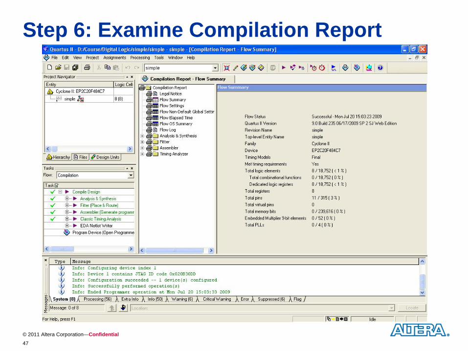
Step 6: Examine Compilation Report
© 2011 Altera Corporation—Confidential48
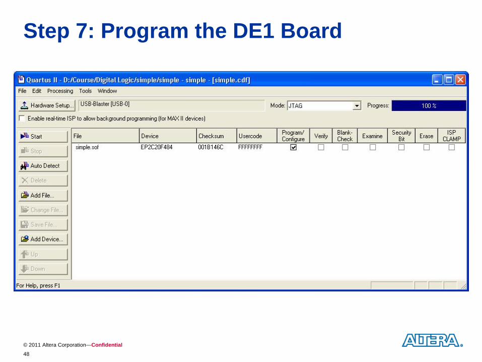
Step 7: Program the DE1 Board
© 2011 Altera Corporation—Confidential49
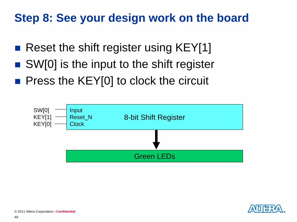
Step 8: See your design work on the board
Reset the shift register using KEY[1]
SW[0] is the input to the shift register
Press the KEY[0] to clock the circuit
Green LEDs
8-bit Shift RegisterInputReset_NClock
SW[0]KEY[1]KEY[0]
© 2011 Altera Corporation—Confidential50
Next Example
Open the Digital Logic Directory
Go into stopper subdirectory
Double-click on stopper.qpf to open an existing project
© 2011 Altera Corporation—Confidential51
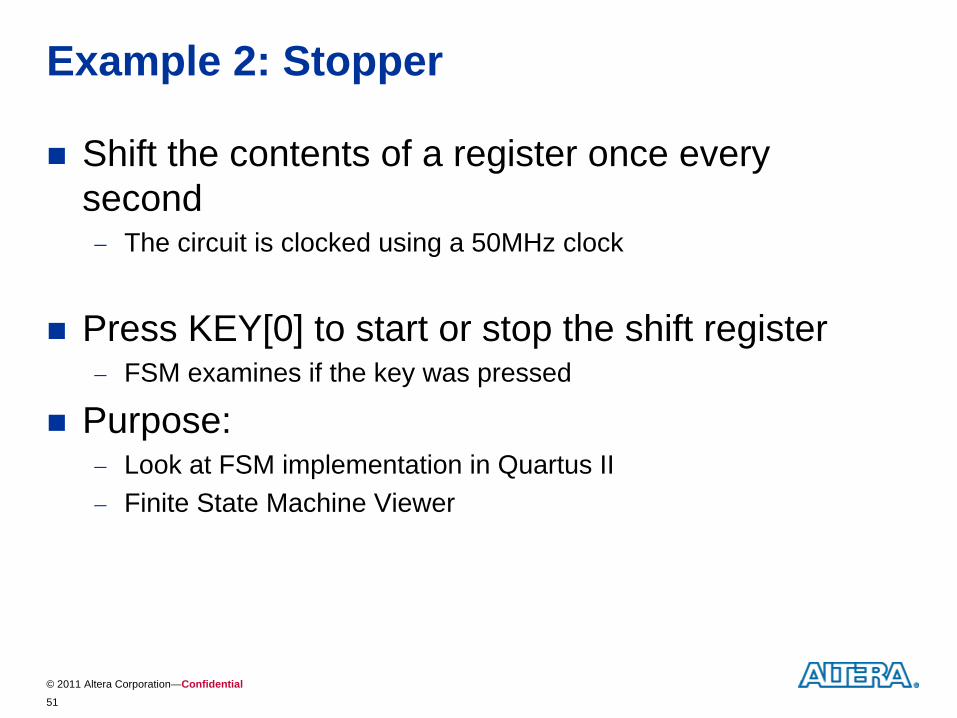
Example 2: Stopper
Shift the contents of a register once every second
The circuit is clocked using a 50MHz clock
Press KEY[0] to start or stop the shift register
FSM examines if the key was pressed
Purpose:
Look at FSM implementation in Quartus II
Finite State Machine Viewer
© 2011 Altera Corporation—Confidential52
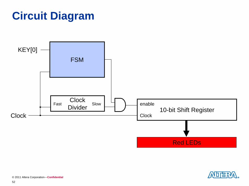
Circuit Diagram
ClockDivider
Fast Slow
Red LEDs
10-bit Shift Registerenable
ClockClock
KEY[0]FSM
© 2011 Altera Corporation—Confidential53
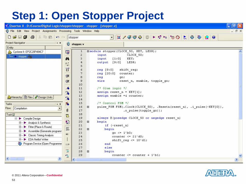
Step 1: Open Stopper Project
© 2011 Altera Corporation—Confidential54
Step 2: Compile and Program
Compile the design
Program the design onto the DE2 board
How does it work?
Press KEY[0] to start/stop the circuit
Press KEY[1] to reset the circuit
© 2011 Altera Corporation—Confidential55
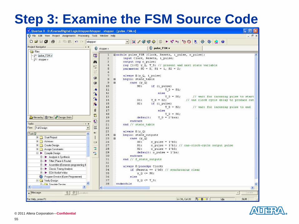
Step 3: Examine the FSM Source Code
© 2011 Altera Corporation—Confidential56
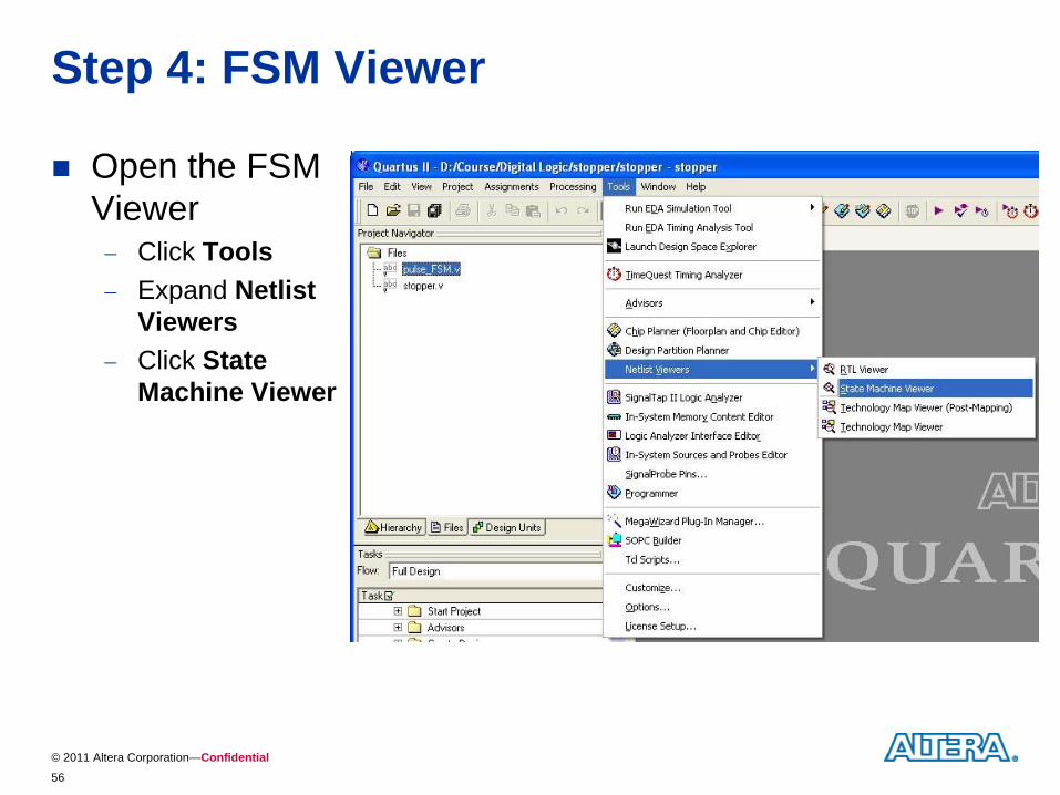
Step 4: FSM Viewer
Open the FSM Viewer
Click Tools
Expand Netlist Viewers
Click State Machine Viewer
© 2011 Altera Corporation—Confidential57
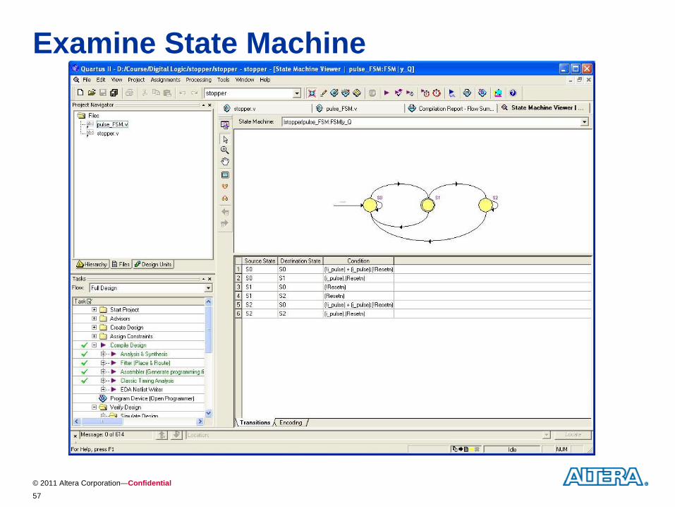
Examine State Machine
© 2011 Altera Corporation—Confidential58
Next Example
Open the Digital Logic Directory
Go into seg_shift subdirectory
Double-click on seg_shift.qpf to open an existing project
© 2011 Altera Corporation—Confidential59
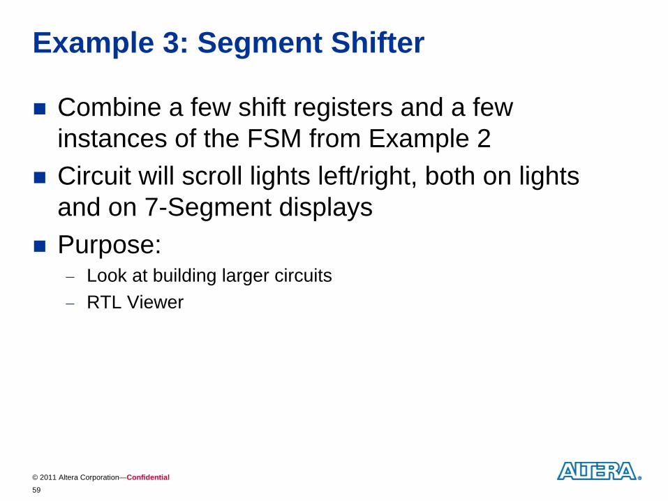
Example 3: Segment Shifter
Combine a few shift registers and a few instances of the FSM from Example 2
Circuit will scroll lights left/right, both on lights and on 7-Segment displays
Purpose:
Look at building larger circuits
RTL Viewer
© 2011 Altera Corporation—Confidential60
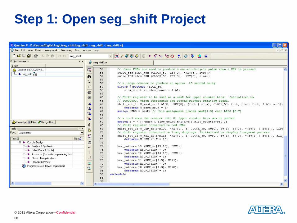
Step 1: Open seg_shift Project
© 2011 Altera Corporation—Confidential61
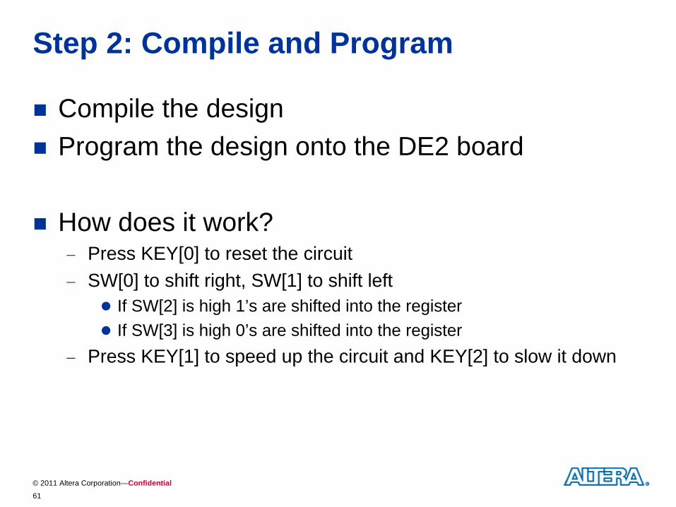
Step 2: Compile and Program
Compile the design
Program the design onto the DE2 board
How does it work?
Press KEY[0] to reset the circuit
SW[0] to shift right, SW[1] to shift left
If SW[2] is high 1’s are shifted into the register
If SW[3] is high 0’s are shifted into the register
Press KEY[1] to speed up the circuit and KEY[2] to slow it down
© 2011 Altera Corporation—Confidential62
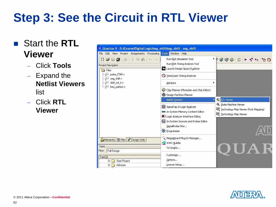
Step 3: See the Circuit in RTL Viewer
Start the RTL Viewer
Click Tools
Expand the Netlist Viewers list
Click RTL Viewer
© 2011 Altera Corporation—Confidential63
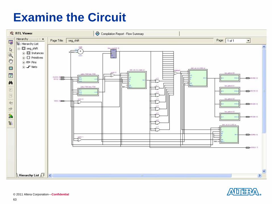
Examine the Circuit
© 2011 Altera Corporation—Confidential64
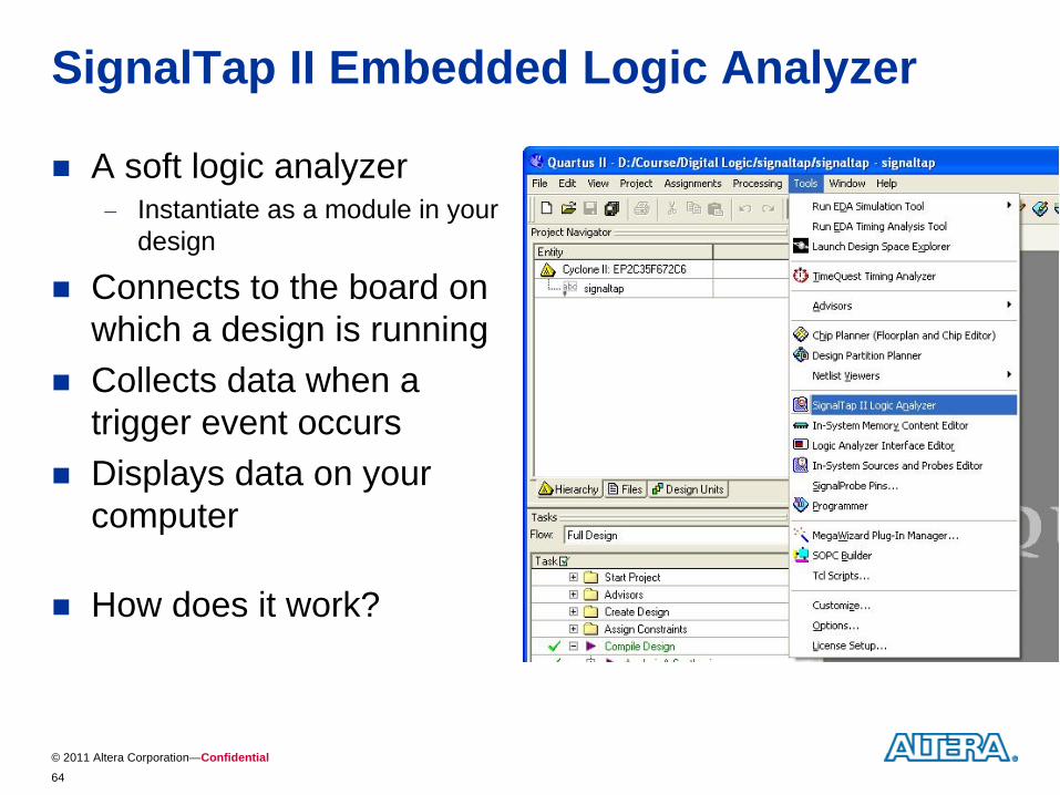
SignalTap II Embedded Logic Analyzer
A soft logic analyzer
Instantiate as a module in your design
Connects to the board on which a design is running
Collects data when a trigger event occurs
Displays data on your computer
How does it work?
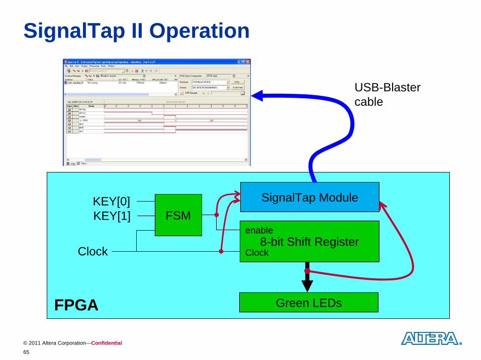
© 2011 Altera Corporation—Confidential65
FPGA
SignalTap II Operation
SignalTap Module
Green LEDs
8-bit Shift Registerenable
ClockClock
FSMKEY[0]KEY[1]
USB-Blastercable
© 2011 Altera Corporation—Confidential66
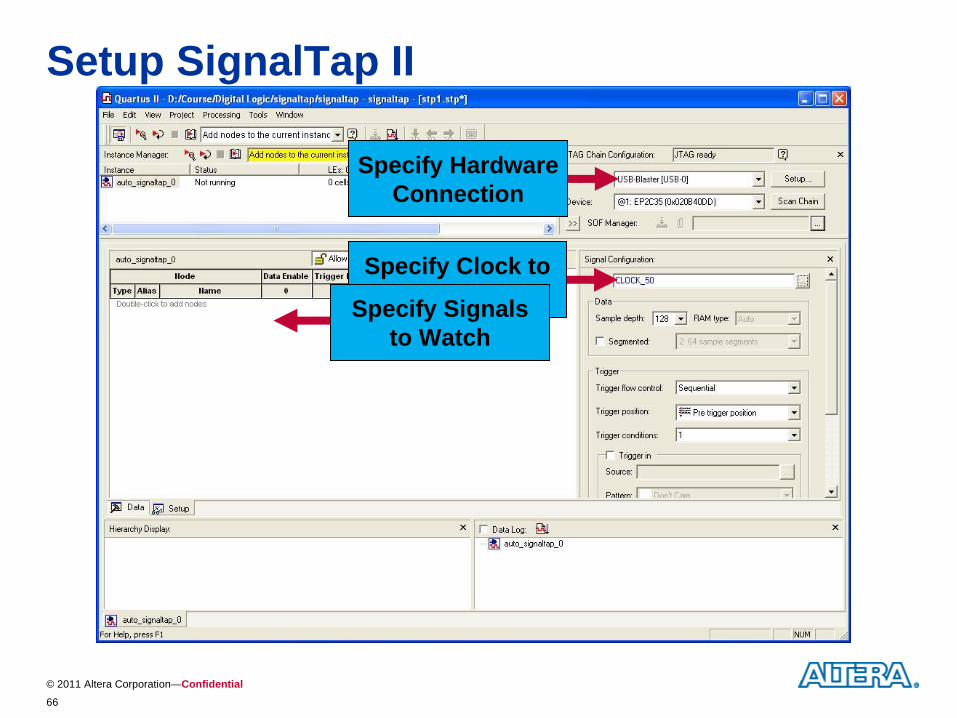
Setup SignalTap II
Specify HardwareConnection
Specify Clock toLatch data onSpecify Signalsto Watch
© 2011 Altera Corporation—Confidential67
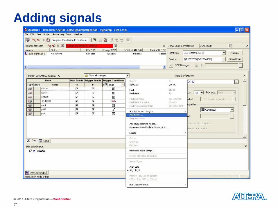
Adding signals
© 2011 Altera Corporation—Confidential68
Recompile Project
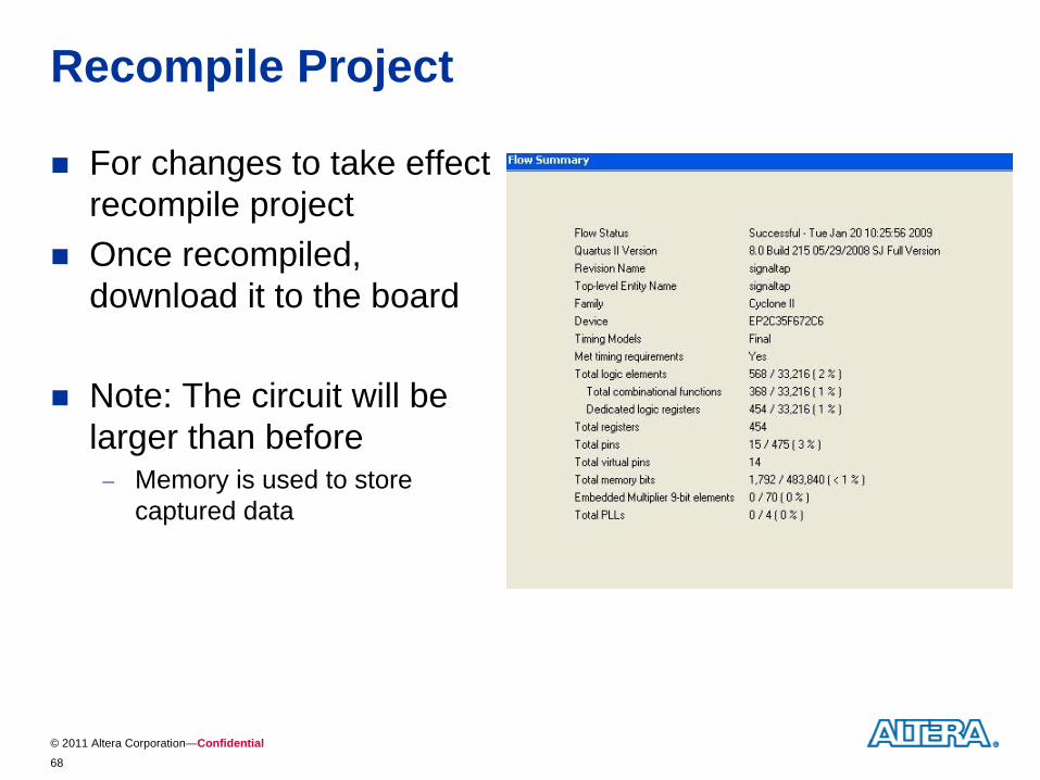
For changes to take effect recompile project
Once recompiled, download it to the board
Note: The circuit will be larger than before
Memory is used to store captured data
© 2011 Altera Corporation—Confidential69
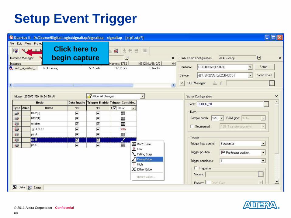
Setup Event Trigger
Click here tobegin capture
© 2011 Altera Corporation—Confidential70
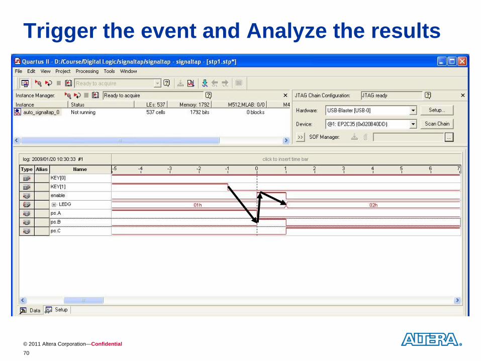
Trigger the event and Analyze the results
© 2011 Altera Corporation—Confidential71
Summary
Learned how to
Use Quartus II CAD Software
Compile projects in Quartus II
Target design onto DE2 board
View results of compilation
Use SignalTapII
Where do we go from here?

© 2011 Altera Corporation—Confidential
Concluding RemarksConcluding Remarks