interconnect optimization for deep-submicron and gigahertz ics
DESCRIPTION
Interconnect Optimization for Deep-Submicron and Gigahertz ICs. Lei He http://cadlab.cs.ucla.edu/~helei UCLA Computer Science Department Los Angeles, CA 90095. Agenda. Background LR-based STIS optimization LR -- local refinement STIS -- simultaneous transistor and interconnect sizing - PowerPoint PPT PresentationTRANSCRIPT

Interconnect Optimization for Deep-Submicron and Gigahertz ICs
Lei HeLei He
http://cadlab.cs.ucla.edu/~heleihttp://cadlab.cs.ucla.edu/~helei
UCLA Computer Science DepartmentUCLA Computer Science Department
Los Angeles, CA 90095Los Angeles, CA 90095

Agenda
Background Background
LR-based STIS optimizationLR-based STIS optimization LR -- local refinementLR -- local refinement STIS -- simultaneous transistor and interconnect sizingSTIS -- simultaneous transistor and interconnect sizing
Conclusions and future worksConclusions and future works

Upcoming Design Challenges
Microprocessors used in server computersMicroprocessors used in server computers 1998 -- 0.25um, 7.5M FETs, 450MHz1998 -- 0.25um, 7.5M FETs, 450MHz 2001 -- 0.18um, ~100M FETs, >1GHz2001 -- 0.18um, ~100M FETs, >1GHz
close to tape-outclose to tape-out 2005 -- 0.10um, ~200M FETS, ~3.5GHz2005 -- 0.10um, ~200M FETS, ~3.5GHz
launch design in 2003launch design in 2003 begin developing design tools in 2001begin developing design tools in 2001 start research right nowstart research right now
We are moving faster than Moore’s LawWe are moving faster than Moore’s Law

Critical Issue: Interconnect Delay
Starting from 0.25um generation, circuit delay is dominated by interconnect delayStarting from 0.25um generation, circuit delay is dominated by interconnect delay Efforts to control interconnect delayEfforts to control interconnect delay
Processing technology: Processing technology: Cu and low K dielectricCu and low K dielectric Design technology:Design technology: interconnect-centric designinterconnect-centric design

Layout Design:Device-Centric versus Interconnect-Centric
Floorplaning
Global Routing
Detailed Routing
Timing Driven PlacementDelay Budgeting
Device-CentricDevice-Centric
FloorplaningInterconnect Planning, and Interconnect Optimization
Global Routingwith Interconnect Optimization
Detailed Routingwith Variable Width and Spacing
Timing Driven PlacementDelay Budgeting
Interconnect-CentricInterconnect-Centric

Topology
Interconnect Optimization
Device locations and constraints:
• Delay
• Power
• Signal integrity
• Skew
...
Automatic solutions guided by accurate interconnect and Automatic solutions guided by accurate interconnect and device modelsdevice models
Sizing
Spacing
Other critical optimizations: buffer insertion, simultaneous Other critical optimizations: buffer insertion, simultaneous device and interconnect sizing …device and interconnect sizing …
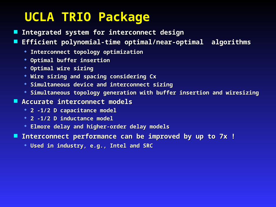
UCLA TRIO Package Integrated system for interconnect designIntegrated system for interconnect design Efficient polynomial-time optimal/near-optimal algorithmsEfficient polynomial-time optimal/near-optimal algorithms
Interconnect topology optimizationInterconnect topology optimization Optimal buffer insertionOptimal buffer insertion Optimal wire sizingOptimal wire sizing Wire sizing and spacing considering CxWire sizing and spacing considering Cx Simultaneous device and interconnect sizingSimultaneous device and interconnect sizing Simultaneous topology generation with buffer insertion and wiresizingSimultaneous topology generation with buffer insertion and wiresizing
Accurate interconnect modelsAccurate interconnect models 2 -1/2 D capacitance model2 -1/2 D capacitance model 2 -1/2 D inductance model2 -1/2 D inductance model Elmore delay and higher-order delay modelsElmore delay and higher-order delay models
Interconnect performance can be improved by up to 7x !Interconnect performance can be improved by up to 7x ! Used in industry, e.g., Intel and SRC Used in industry, e.g., Intel and SRC

UCLA TRIO Package Integrated system for interconnect designIntegrated system for interconnect design Efficient polynomial-time optimal/near-optimal algorithmsEfficient polynomial-time optimal/near-optimal algorithms
Interconnect topology optimizationInterconnect topology optimization Optimal buffer insertionOptimal buffer insertion Optimal wire sizing Optimal wire sizing [Cong-He, ICCAD’95, TODAES’96][Cong-He, ICCAD’95, TODAES’96] Wire sizing and spacing considering Cx Wire sizing and spacing considering Cx [Cong-He+, ICCAD’97, TCAD’99][Cong-He+, ICCAD’97, TCAD’99] Simultaneous device and interconnect sizing Simultaneous device and interconnect sizing [Cong-He, ICCAD’96, TCAD’99][Cong-He, ICCAD’96, TCAD’99]
Simultaneous topology generation with buffer insertion and wiresizingSimultaneous topology generation with buffer insertion and wiresizing
Accurate interconnect modelsAccurate interconnect models 2 -1/2 D capacitance model 2 -1/2 D capacitance model [Cong-He-Kahng+, DAC’97] [Cong-He-Kahng+, DAC’97] (with Cadence)(with Cadence) 2 -1/2 D inductance model 2 -1/2 D inductance model [He-Chang-Lin+, CICC’99] [He-Chang-Lin+, CICC’99] (with HP Labs)(with HP Labs)
Elmore delay and higher-order delay modelsElmore delay and higher-order delay models
Interconnect performance can be improved by up to 7x !Interconnect performance can be improved by up to 7x ! Used in industry, e.g., Intel and SRCUsed in industry, e.g., Intel and SRC

Agenda
BackgroundBackground
LR-based STIS optimizationLR-based STIS optimization Motivation for LR-based optimizationMotivation for LR-based optimization
Conclusions and future worksConclusions and future works

Discrete Wiresizing Optimization[Cong-Leung, ICCAD’93]
Given: A set of possible wire widths { WGiven: A set of possible wire widths { W11, W, W22, …, W, …, Wrr } }
Find: An optimal wire width assignment to minimize Find: An optimal wire width assignment to minimize weighted sum of sink delays weighted sum of sink delays
WiresizingOptimizatio
n

Dominance Relation and Local Refinement
Dominance RelationDominance Relation For all For all EEj j , w(E, w(Ej j )) w'(E w'(Ej j ))
W dominates W’ (i.e., W W’)
WW
W’W’
Local refinement (LR)Local refinement (LR) LR for ELR for E11 to find an optimal to find an optimal
width for Ewidth for E11, assuming widths , assuming widths for other wires are fixed with for other wires are fixed with respect to current width respect to current width assignment assignment
Single-variable optimization Single-variable optimization can be solved efficientlycan be solved efficiently

Dominance Property for Discrete Wiresizing[Cong-Leung, ICCAD’93]
If solution If solution WW dominates optimal solution dominates optimal solution W*W* W’W’ = local refinement of = local refinement of WW
Then, Then, W’W’ dominates dominates W*W*
If solution If solution WW is dominated by optimal solution is dominated by optimal solution W*W* W’W’ = local refinement of = local refinement of WW
Then, Then, W’W’ is dominated by is dominated by W*W*
A highly efficient algorithm to compute A highly efficient algorithm to compute tight lower and upper bounds of optimal solutiontight lower and upper bounds of optimal solution
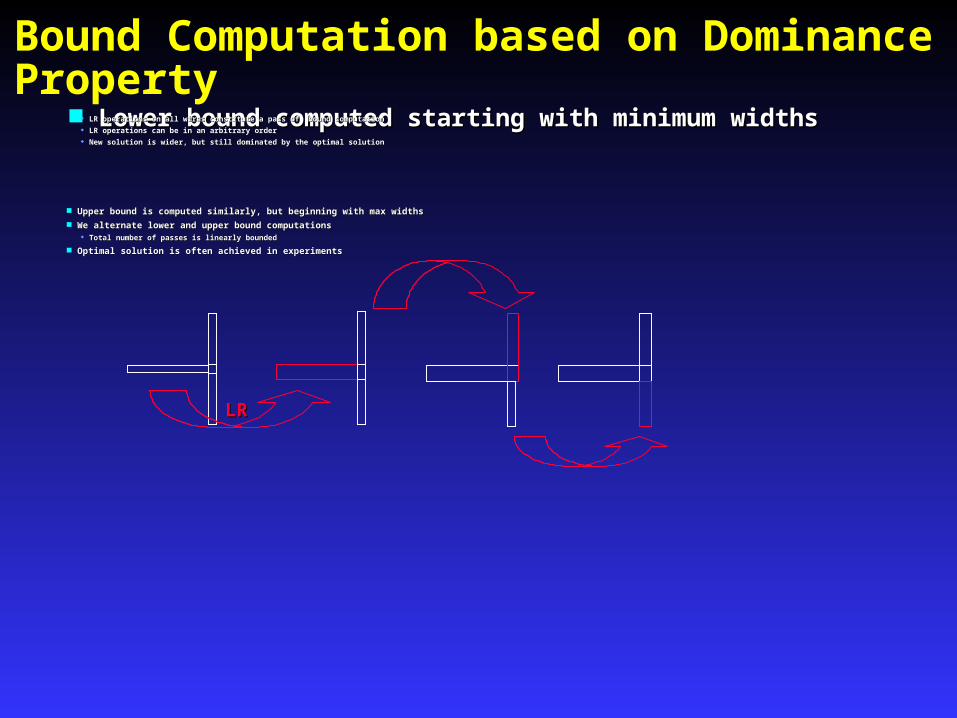
Bound Computation based on Dominance Property
Lower bound computed starting with minimum widthsLower bound computed starting with minimum widths LR operations on all wires constitute a pass of bound computationLR operations on all wires constitute a pass of bound computation LR operations can be in an arbitrary orderLR operations can be in an arbitrary order New solution is wider, but still dominated by the optimal solution New solution is wider, but still dominated by the optimal solution
Upper bound is computed similarly, but beginning with max widthsUpper bound is computed similarly, but beginning with max widths We alternate lower and upper bound computations We alternate lower and upper bound computations
Total number of passes is linearly boundedTotal number of passes is linearly bounded
Optimal solution is often achieved in experimentsOptimal solution is often achieved in experiments
LRLR

Other Problems Solved by LR operation
Multi-source discrete wiresizing Multi-source discrete wiresizing [Cong-He, ICCAD’95][Cong-He, ICCAD’95]
Bundled-LR is proposed to speed up LR by a factor of 100xBundled-LR is proposed to speed up LR by a factor of 100x Continuous wiresizing Continuous wiresizing [Chen-Wong, ISCAS’96][Chen-Wong, ISCAS’96]
Linear convergence is proved Linear convergence is proved [Chu-Wong, TCAD’99][Chu-Wong, TCAD’99]
Simultaneous buffer and wire sizing Simultaneous buffer and wire sizing [Chen-Chang-Wong, [Chen-Chang-Wong, DAC’96]DAC’96] Extended to general gates and multiple netsExtended to general gates and multiple nets [Chu-Chen-Wong, [Chu-Chen-Wong,
ICCAD’98]ICCAD’98]
Why LR operation works?Why LR operation works?
Agenda
BackgroundBackground
LR-based STIS optimizationLR-based STIS optimization Motivation of LR-based optimizationMotivation of LR-based optimization Simple CH-program and application to STIS problemSimple CH-program and application to STIS problem
Conclusions and future worksConclusions and future works

Simple CH-function [Cong-He, ICCAD’96, TCAD’99]
It includes the objective functions for a number of worksIt includes the objective functions for a number of works Discrete or continuous wire sizing Discrete or continuous wire sizing [Cong-Leung, ICCAD’93][Cong-He, ICCAD’95][Chen-Wong,ISCAS’96][Cong-Leung, ICCAD’93][Cong-He, ICCAD’95][Chen-Wong,ISCAS’96] Simultaneous device and wire sizingSimultaneous device and wire sizing [Cong-Koh, ICCAD’94][Chen-Chang-Wong, DAC’96][Cong-Koh-Leung, [Cong-Koh, ICCAD’94][Chen-Chang-Wong, DAC’96][Cong-Koh-Leung,
ILPED’96][Chu-Chen-Wong, ICCAD’98]ILPED’96][Chu-Chen-Wong, ICCAD’98]
is a simple CH-functionis a simple CH-function Coefficients Coefficients aapipi andand b bqjqj are positive constants are positive constants
Examples:Examples:

Simple CH-Program and Dominance Property
To minimize a CH-function is a CH-program. To minimize a CH-function is a CH-program.
Theorem:Theorem: The dominance property holds for simple CH-program w.r.t. theThe dominance property holds for simple CH-program w.r.t. the
LR operation.LR operation. If If XX dominates optimal solution dominates optimal solution X*X*
X’X’ = local refinement of = local refinement of XXThen, Then, X’X’ dominates dominates X*X*
If If XX is dominated by is dominated by X*X*X’X’=local refinement of =local refinement of XXThen, Then, X’X’ is dominated by is dominated by X*X*

Simple CH-function [Cong-He, ICCAD’96, TCAD’99]
It includes the objective functions for a number of worksIt includes the objective functions for a number of works Discrete or continuous wire sizing Discrete or continuous wire sizing [Cong-Leung, ICCAD’93][Cong-He, ICCAD’95][Chen-Wong,ISCAS’96][Cong-Leung, ICCAD’93][Cong-He, ICCAD’95][Chen-Wong,ISCAS’96] Simultaneous device and wire sizingSimultaneous device and wire sizing [Cong-Koh, ICCAD’94][Chen-Chang-Wong, DAC96][Cong-Koh-Leung, [Cong-Koh, ICCAD’94][Chen-Chang-Wong, DAC96][Cong-Koh-Leung,
ILPED’96][Chu-Chen-Wong, ICCAD’98]ILPED’96][Chu-Chen-Wong, ICCAD’98]
is a simple CH-functionis a simple CH-function Coefficients Coefficients aapipi andand b bqjqj are positive constants are positive constants
Examples:Examples: Unified and efficient solutionUnified and efficient solution

General Formulation: STIS Simultaneous Transistor and Interconnect Sizing
Given:Given: Circuit netlist and initial layout design Circuit netlist and initial layout design Determine: Discrete sizes for devices/wiresDetermine: Discrete sizes for devices/wires Minimize:Minimize: Delay + Delay + Power + Power + Area Area
It is the first publication to consider simultaneous It is the first publication to consider simultaneous device and wire sizing device and wire sizing for complex gates and multiple for complex gates and multiple pathspaths

unit-width resistanceunit-width resistance unit-width area capacitanceunit-width area capacitance effective-fringing capacitance effective-fringing capacitance discrete widths and variables for discrete widths and variables for
optimizationoptimization
STIS Objective for Delay Minimization
It is a simple CH-function under It is a simple CH-function under simple modelsimple model assuming assuming RR00, , CC00 and and CC11 are are constantsconstants
STIS can be solved by computing lower and upper bounds via LR STIS can be solved by computing lower and upper bounds via LR operationsoperations Identical lower and upper bounds often achievedIdentical lower and upper bounds often achieved
Res = RRes = R0 0 /x/xCap = CCap = C0 0 * x + (C* x + (Cff + C + Cxx) ) = C= C0 0 * x + C* x + C11

SPICE-Delay reduction of LR-Based STIS STIS optimization versus manual optimization for clock STIS optimization versus manual optimization for clock
net [Chien-et al.,ISCC’94]: net [Chien-et al.,ISCC’94]: 1.2um process, 41518.2 um wire, 154 inverters 1.2um process, 41518.2 um wire, 154 inverters
Two formulations for LR-based optimizationTwo formulations for LR-based optimization sgws sgws simultaneous gate and wire sizingsimultaneous gate and wire sizing stisstis simultaneous transistor and interconnect sizingsimultaneous transistor and interconnect sizing
manual sgws stis
max delay (ns) 4.6324 4.34 (-6.2%) 3.96 (-14.4)power(mW) 60.85 46.1 (-24.3%) 46.3 (-24.2%)clock skew (ps) 470 130 (-3.6x) 40 (-11.7x)
Runtime (wire segmenting: 10um) Runtime (wire segmenting: 10um) LR-based LR-based sgwssgws 1.18s, 1.18s, stisstis 0.88s 0.88s HSPICE simulation HSPICE simulation ~2100s in total ~2100s in total

unit-width resistanceunit-width resistance unit-width area capacitance unit-width area capacitance fringing capacitance fringing capacitance discrete widths and variables for discrete widths and variables for
optimizationoptimization
STIS Objective for Delay Minimization
It is a simple CH-functionIt is a simple CH-function under simple model assuming under simple model assuming RR00 , ,CC00 and and CC11 are constants are constants
Over-simplified for DSM (Deep Submicron) designsOver-simplified for DSM (Deep Submicron) designs

R0 is far away from a Constant!
RR00 depends on size, input slope t depends on size, input slope ttt and output load c and output load cll
May differ by a factor of 2May differ by a factor of 2
size = 100x
cl \ tt 0.05ns 0.10ns 0.20ns
0.225pf 12200 12270 191800.425pf 8135 9719 125000.825pf 8124 8665 10250
size = 400x
cl \ tt 0.05ns 0.10ns 0.20ns
0.501pf 12200 15550 191500.901pf 11560 13360 174401.701pf 8463 9688 12470
effective-resistance R0 for unit-width n-transistor
Using more accurate model like the table-based device model has the potential of Using more accurate model like the table-based device model has the potential of further delay reduction.further delay reduction. But easy to be trapped at local optimum, and tends to be even worse than using simple But easy to be trapped at local optimum, and tends to be even worse than using simple
model model [Fishburn-Dunlop, ICCAD’85][Fishburn-Dunlop, ICCAD’85]

Neither C0 nor C1 is a Constant Both depend on wire width and spacingBoth depend on wire width and spacing
Especially CEspecially C11 = C = Cff +C +Cx x is sensitive to spacingis sensitive to spacing
CCx x accounts for >50% capacitance in DSMaccounts for >50% capacitance in DSM Proper spacing may lead to extra delay reductionProper spacing may lead to extra delay reduction But no existing automatic algorithmBut no existing automatic algorithm
E1 E1
spacingspacing
0
0.05
0.1
0.15
0.2
0.25
0.3
50 100 150 200 250 300
Effective-fringecapacitance(fF/um)
Spacing (nm)Spacing (nm)

STIS-DSM Problem to Consider DSM Effects
STIS-DSM problemSTIS-DSM problem Find: Find: device sizing, and wire sizing and spacing solution device sizing, and wire sizing and spacing solution optimal optimal
with respect to accurate device model and multiple netswith respect to accurate device model and multiple nets
Easier but less appealing formulation: single-net STIS-DSMEasier but less appealing formulation: single-net STIS-DSM Find: Find: device sizing, and wire sizing and spacing solution device sizing, and wire sizing and spacing solution optimal optimal
with respect to accurate device model and with respect to accurate device model and a single-neta single-net Assume: its neighboring wires are fixedAssume: its neighboring wires are fixed
STIS-DSMSTIS-DSM
Agenda
BackgroundBackground
LR-based STIS optimizationLR-based STIS optimization Motivation: LR-based wire sizingMotivation: LR-based wire sizing Simple CH-program and application to STIS problemSimple CH-program and application to STIS problem Bundled CH-program and application to STIS-DSM Bundled CH-program and application to STIS-DSM
problemproblem
Conclusions and future worksConclusions and future works

Go beyond Simple CH-function
It is a simple CH-function ifIt is a simple CH-function if aapipi and and bbqjqj are positive constantsare positive constants
It is a bounded CH-function ifIt is a bounded CH-function if aapipi and and bbqjqj are are functions of functions of XX aapipi and and bbqj qj are positive and boundedare positive and bounded
and and
Examples: Examples:
Objective function for STIS-DSM problemObjective function for STIS-DSM problem

Extended-LR Operation
Extended-LR (ELR) operation is a relaxed LR operationExtended-LR (ELR) operation is a relaxed LR operation Replace Replace aapipi and and bbqj qj by its lower or upper bound during LR operation to assure that by its lower or upper bound during LR operation to assure that
the resulting lower or upper bound isthe resulting lower or upper bound is always correct always correct Lower and upper bounds might be conservativeLower and upper bounds might be conservative..
Example: Example: ELR for a lower bound isELR for a lower bound is
ELR for an upper bound isELR for an upper bound is ??

Theorem (Theorem ([Cong-He, TCAD’99][Cong-He, TCAD’99])) Dominance property holds for bundled CH-program with respect to Dominance property holds for bundled CH-program with respect to
ELR operationELR operation
General Dominance Property
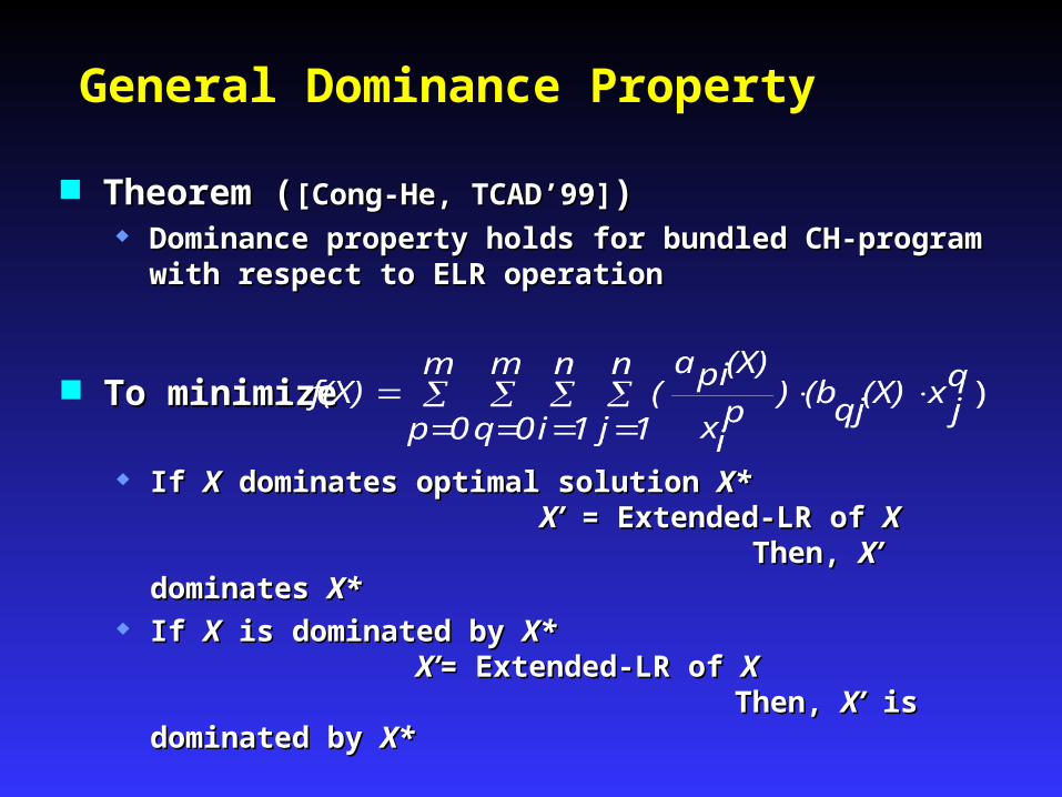
Theorem (Theorem ([Cong-He, TCAD’99][Cong-He, TCAD’99])) Dominance property holds for bundled CH-program with respect to Dominance property holds for bundled CH-program with respect to
ELR operationELR operation
General Dominance Property
To minimize To minimize
If If XX dominates optimal solution dominates optimal solution X*X* X’X’ = Extended-LR of = Extended-LR of XX
Then, Then, X’X’ dominates dominates X*X* If If XX is dominated by is dominated by X*X*
X’X’= Extended-LR of = Extended-LR of XX Then, Then, X’X’ is dominated by is dominated by X*X*

STIS-DSM can be solved as a bundled CH-programSTIS-DSM can be solved as a bundled CH-program Lower bound computed by ELR starting with minimum sizesLower bound computed by ELR starting with minimum sizes Upper bound computed by ELR starting with maximum sizesUpper bound computed by ELR starting with maximum sizes Lower and upper bound computations are alternated to shrink solution spaceLower and upper bound computations are alternated to shrink solution space
Up-to-date lower and upper bounds of RUp-to-date lower and upper bounds of R0 0 , C, C0 0 and Cand C1 1 are usedare used Uncertainty of RUncertainty of R0 0 , C, C0 0 and Cand C1 1 is reduced when the solution space is shrunkis reduced when the solution space is shrunk
There exists an optimal solution to the STIS-DSM problem between final lower and upper boundsThere exists an optimal solution to the STIS-DSM problem between final lower and upper bounds
Solution to STIS-DSM Problem

Gaps between Lower and Upper Bounds Two nets under 0.18um technology:Two nets under 0.18um technology: DCLK DCLK and and 2cm line 2cm line
STIS-DSM uses table-based device model and ELR operationSTIS-DSM uses table-based device model and ELR operation STIS uses simple device model and LR operationSTIS uses simple device model and LR operation
We report average width / average gapWe report average width / average gap
DCLK STIS STIS-DSM STIS STIS-DSM
sgws 5.39/0.07 13.0/1.91 2.50/0.003 2.78/0.025
stis 17.2/1.53 21.6/2.36 2.69/0.017 2.82/0.030
2cm line STIS STIS-DSM STIS STIS-DSM
sgws 108/0.108 112/0.0 4.98/0.004 4.99/0.106
stis 126/0.97 125/1.98 5.05/0.032 5.11/0.091
Transistors Wires
Gap is about 1% of width in most casesGap is about 1% of width in most cases

STIS-DSM versus STIS STIS-DSM versus STIS STIS-DSM uses table-based device model and ELR operationSTIS-DSM uses table-based device model and ELR operation STIS uses simple device model and LR operationSTIS uses simple device model and LR operation
DCLK STIS STIS-DSM
sgws 1.16 (0.0%) 1.08 (-6.8%)
stis 1.13 (0.0%) 0.96 (-15.1%)
2cm line STIS STIS-DSM
sgws 0.82 (0.0%) 0.81 (-0.4%)
stis 0.75 (0.0%) 0.69 (-7.6%)
STIS-DSM achieves up to 15% extra reductionSTIS-DSM achieves up to 15% extra reduction Runtime is still impressiveRuntime is still impressive
Total optimization timeTotal optimization time ~10 seconds~10 seconds
Delay Reduction by Accurate Device Model
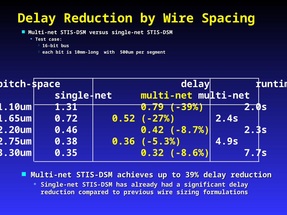
Delay Reduction by Wire Spacing
Multi-net STIS-DSM achieves up to 39% delay reductionMulti-net STIS-DSM achieves up to 39% delay reduction Single-net STIS-DSM has already had a significant delay reduction compared to Single-net STIS-DSM has already had a significant delay reduction compared to
previous wire sizing formulations previous wire sizing formulations
pitch-space delay runtimesingle-net multi-net multi-net
1.10um 1.31 0.79 (-39%) 2.0s1.65um 0.72 0.52 (-27%) 2.4s2.20um 0.46 0.42 (-8.7%) 2.3s2.75um 0.38 0.36 (-5.3%) 4.9s3.30um 0.35 0.32 (-8.6%) 7.7s
Multi-net STIS-DSM versus single-net STIS-DSMMulti-net STIS-DSM versus single-net STIS-DSM Test case:Test case:
16-bit bus16-bit bus each bit is 10mm-long with 500um per segmenteach bit is 10mm-long with 500um per segment

Valid for general problemsValid for general problems
Conclusions Interconnect-centric design is the key to DSM and GHz IC designs Interconnect-centric design is the key to DSM and GHz IC designs Interconnect optimization is able to effectively control Interconnect optimization is able to effectively control
interconnect delayinterconnect delay Problem formulations should consider DSM effectsProblem formulations should consider DSM effects
e.g., LR-based optimization for STIS-DSM probleme.g., LR-based optimization for STIS-DSM problem
More is needed to close the loop of interconnect-centric designMore is needed to close the loop of interconnect-centric design Interconnect planningInterconnect planning Interconnect optimization for noise, and inductanceInterconnect optimization for noise, and inductance Interconnect verification, especially for pattern-dependent noise and delayInterconnect verification, especially for pattern-dependent noise and delay … … ... ...