intel txn13220/1/4/5/7/8 sff 10 gbps optical transceiver ... · optical transceiver with 16-channel...
TRANSCRIPT
Order Number: 273807, 004
26-Oct-2006
Intel® TXN13220/1/4/5/7/8 SFF 10 Gbps Optical Transceiver with 16-Channel Multiplexer/Demultiplexer
Datasheet
Product Features
Applications
� 10 Gbps Optical Transmitter and Receiver Pair with 16 Channel Multiplexer/Demultiplexer
� Typical Receiver Sensitivity < -14 dBm
� Available in Short-Reach (7 km, 12 km, 25 km) and Intermediate-Reach (40 km) Versions
� 300-Pin Multi-Source Agreement Compatible Form Factor and Pin Configuration
� LVDS Data Interface through 300-Pin, Berg Connector
� Optional Jitter Filter
� 9-Bit-Deep FIFO Buffer
� Integral Heat Sinking Designed for 250 Linear Feet per Minute, 55 °C Ambient Air Flow; Flat Top Version Also Available
� Case Operating Temperature -5 °C to 70 °C
� Laser Bias, Laser Temperature, Laser Power, and Receiver Power Monitors
� Receive and Transmit Loss-of-Lock, Receive Loss-of-Avg-Power, Laser Bias, and Laser Temperature Alarms
� Multi-Rate Capability, Digitally Selectable between SONET 9.953 Gbps and FEC 10.709 Gbps Rates or 10Gb Ethernet 10.3 Gbps
� Includes Active Signal Monitoring and Onboard Microprocessor which Uses the I2C Bus
� 1310 nm and 1550 nm Wavelength
Client-side interfaces of Metro/Core Equipment, including:
� Core-enterprise Switches, and Routers
� Multi-service Provisioning Platforms
� Cross-Connects
� Add/Drop Multiplexers
� Dense Wavelength Division Multiplex Terminals
� Other WDM and Non-WDM Metro System Equipment
� Optical Test Equipment
� Optical Transport Solutions

Intel® TXN13220/1/4/5/7/8 SFF 10 Gbps Optical TransceiverDatasheet 26-Oct-20062 Order Number: 273807004
Legal Lines and DisclaimersINFORMATION IN THIS DOCUMENT IS PROVIDED IN CONNECTION WITH INTEL® PRODUCTS. NO LICENSE, EXPRESS OR IMPLIED, BY ESTOPPEL OR OTHERWISE, TO ANY INTELLECTUAL PROPERTY RIGHTS IS GRANTED BY THIS DOCUMENT. EXCEPT AS PROVIDED IN INTEL'S TERMS AND CONDITIONS OF SALE FOR SUCH PRODUCTS, INTEL ASSUMES NO LIABILITY WHATSOEVER, AND INTEL DISCLAIMS ANY EXPRESS OR IMPLIED WARRANTY, RELATING TO SALE AND/OR USE OF INTEL PRODUCTS INCLUDING LIABILITY OR WARRANTIES RELATING TO FITNESS FOR A PARTICULAR PURPOSE, MERCHANTABILITY, OR INFRINGEMENT OF ANY PATENT, COPYRIGHT OR OTHER INTELLECTUAL PROPERTY RIGHT. Intel products are not intended for use in medical, life saving, life sustaining, critical control or safety systems, or in nuclear facility applications.
Intel may make changes to specifications and product descriptions at any time, without notice.
Intel Corporation may have patents or pending patent applications, trademarks, copyrights, or other intellectual property rights that relate to the presented subject matter. The furnishing of documents and other materials and information does not provide any license, express or implied, by estoppel or otherwise, to any such patents, trademarks, copyrights, or other intellectual property rights.
The Intel® TXN13220/7/8 Optical Transceiver may contain design defects or errors known as errata which may cause the product to deviate from published specifications. Current characterized errata are available on request.
Contact your local Intel sales office or your distributor to obtain the latest specifications and before placing your product order.
Copies of documents which have an order number and are referenced in this document, or other Intel literature may be obtained by calling 1-800-548-4725 or by visiting Intel's website at http://www.intel.com.
Intel and the Intel logo are trademarks or registered trademarks of Intel Corporation or its subsidiaries in the United States and other countries.
*Other names and brands may be claimed as the property of others.
Copyright © 2005-2006, Intel Corporation. All Rights Reserved.
Intel® TXN13220/1/4/5/7/8 SFF 10 Gbps Optical Transceiver26-Oct-2006 DatasheetOrder Number: 273807, Revision 004 3
Intel® TXN13220/1/4/5/7/8 SFF 10 Gbps Optical Transceiver
Contents
1.0 Introduction ..............................................................................................................8
1.1 Product Overview ................................................................................................8
1.2 Related Hardware and Documents ....................................................................... 10
2.0 Ratings .................................................................................................................... 11
3.0 Product Configurations and Specifications ............................................................... 12
3.1 Product Configurations ....................................................................................... 13
3.1.1 Summary of Product Configurations .......................................................... 13
3.1.2 Intel® TXN132201013 / TXN132251013 Transceivers.................................. 15
3.1.3 Intel® TXN132271013 / TXN132241013 / TXN132282013 Transceivers ......... 16
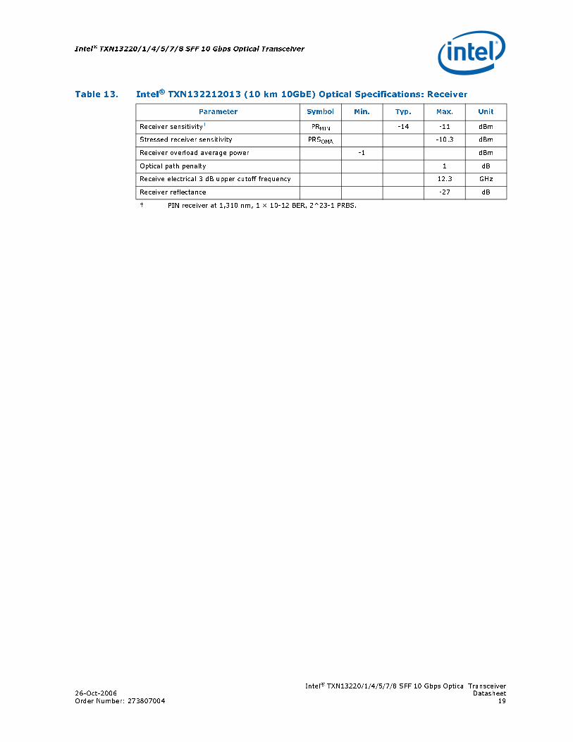
3.1.4 Intel® TXN132212013 Transceiver............................................................ 18
3.1.5 Intel® TXN132204013 / TXN132274013 Transceiver ................................... 20
3.1.6 Intel® TXN132203015 / TXN132273015 Transceivers.................................. 21
3.1.7 Intel® TXN132204015 / TXN132254015 Transceivers.................................. 22
3.1.8 Intel® TXN132274015 / TXN132244015 / TXN132284015 Transceiver........... 23
3.1.9 Intel® TXN132214015 Transceiver............................................................ 25
3.2 Timing ............................................................................................................. 27
3.3 Control and Monitoring Functions......................................................................... 29
3.4 Data Input/Output Configuration ......................................................................... 32
3.5 Pin Configuration............................................................................................... 33
3.6 Input and Output Termination Description ............................................................ 34
3.7 Integrated Power Supply Sequencing ................................................................... 43
3.8 Mechanical Layout and Configuration ................................................................... 43
4.0 Regulatory Compliance ............................................................................................ 47
4.1 Electromagnetic Compatibility Compliance ............................................................ 47
4.2 Safety Compliance............................................................................................. 48
4.3 Compliance with Restriction of Hazardous Substances ............................................ 48
4.4 Product Certification Markings and Compliance Statements ..................................... 49
5.0 Ordering Information .............................................................................................. 50
6.0 Acronyms ................................................................................................................ 51
Figures1 Block Diagram ...........................................................................................................9
2 Intel® TXN13220/1/4/5/7/8 Transceiver – Demux Timing Diagram ................................. 27
3 Intel® TXN13220/1/4/5/7/8 Transceiver – Mux Timing Diagram ..................................... 28
4 Heatsink “A” – 3" x 2.2" × 0.53" ................................................................................ 43
5 Heatsink “B” – 3" x 2.2" × 0.63" ................................................................................ 44
6 Heatsink “C” – 3" x 2.2" × 0.7".................................................................................. 45
7 Heatsink “D” – 3" x 2.2" × 0.53" Flat Top.................................................................... 46
8 Ordering Information................................................................................................ 50
Intel® TXN13220/1/4/5/7/8 SFF 10 Gbps Optical Transceiver
Intel® TXN13220/1/4/5/7/8 SFF 10 Gbps Optical TransceiverDatasheet 26-Oct-20064 Order Number: 273807Revision 004
Tables1 Related Hardware and Documents ..............................................................................10
2 Absolute Maximum Ratings ........................................................................................11
3 Power Supply Requirements.......................................................................................11
4 Product Configurations ..............................................................................................13
5 Intel® TXN132201013 / TXN132251013 (7 km SONET) Optical Specifications: Transmitter .............................................................................................................15
6 Intel® TXN132201013 / TXN132251013 (7 km SONET) Optical Specifications: Link ........................................................................................................................15
7 Intel® TXN132201013 / TXN132251013 (7 km SONET) Optical Specifications: Receiver..................................................................................................................15
8 Intel® TXN132271013 / TXN132241013 / TXN132282013 (7/10 km SONET/10 GbE) Optical Specifications: Transmitter.........................................16
9 Intel® TXN132271013 / TXN132241013 / TXN132282013 (7/10 km SONET/10 GbE) Optical Specifications: Link ...................................................16
10 Intel® TXN132271013 / TXN132241013 / TXN132282013 (7/10 km SONET/10 GbE) Optical Specifications: Receiver .............................................17
11 Intel® TXN132212013 (10 km 10GbE) Optical Specifications: Transmitter........................18
12 Intel® TXN132212013 (10 km 10GbE) Optical Specifications: Link ..................................18
13 Intel® TXN132212013 (10 km 10GbE) Optical Specifications: Receiver ............................19
14 Intel® TXN132204013/TXN132274013 (20 km SONET) Optical Specifications:Transmitter .............................................................................................................20
15 Intel® TXN132204013/TXN132274013 (20 km SONET) Optical Specifications:Link........................................................................................................................20
16 Intel® TXN132204013/TXN132274013 (20 km SONET) Optical Specifications:Receiver..................................................................................................................20
17 Intel® TXN132203015 / TXN132273015 (25 km SONET) Optical Specifications: Transmitter..............................................................................21
18 Intel® TXN132203015 / TXN132273015 (25 km SONET) Optical Specifications: Link ........................................................................................21
19 Intel® TXN132203015 / TXN132273015 (25 km SONET) Optical Specifications: Receiver ..................................................................................21
20 Intel® TXN132204015 / TXN132254015 (40 km SONET) Optical Specifications: Transmitter..............................................................................22
21 Intel® TXN132204015 / TXN132254015 (40 km SONET) Optical Specifications: Link ........................................................................................22
22 Intel® TXN132204015 / TXN132254015 (40 km SONET) Optical Specifications: Receiver ..................................................................................22
23 Intel® TXN132274015 / TXN132244015 / TXN132284015 (40 km SONET/10 GbE) Optical Specifications: Transmitter ............................................23
24 Intel® TXN132274015 / TXN132244015 / TXN132284015 (40 km SONET/10 GbE) Optical Specifications: Link ......................................................23
25 Intel® TXN132274015 / TXN132244015 / TXN132284015(40 km SONET/10 GbE) Optical Specifications: Receiver ................................................24
26 Intel® TXN132214015 (40 km 10 GbE) Optical Specifications: Transmitter .............................................................................................................25
27 Intel® TXN132214015 (40 km SONET/10 GbE) Optical Specifications: Link ........................................................................................................................25
28 Intel® TXN132214015 (40 km SONET/10 GbE) Optical Specifications: Receiver..................................................................................................................26
29 Intel® TXN13220/1/4/5/7/8 Transceiver – Demux Timing-Diagram Parameters ................27
30 Intel® TXN13220/1/4/5/7/8 Transceiver – Mux Timing-Diagram Parameters ....................28
31 Analog Monitoring Signals and Characteristics ..............................................................29
32 Digital Alarms ..........................................................................................................30
33 Digital Control Signals and I2C Bus .............................................................................30
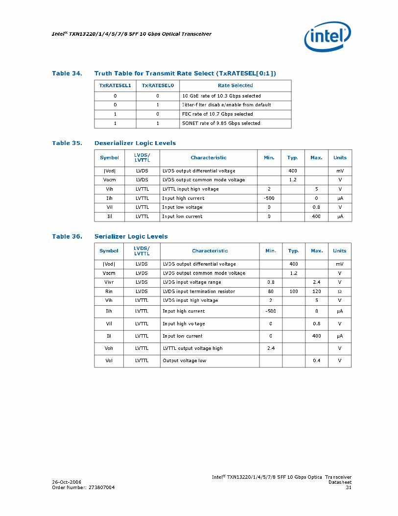
34 Truth Table for Transmit Rate Select (TxRATESEL[0:1]).................................................31
Intel® TXN13220/1/4/5/7/8 SFF 10 Gbps Optical Transceiver26-Oct-2006 DatasheetOrder Number: 273807, Revision 004 5
Intel® TXN13220/1/4/5/7/8 SFF 10 Gbps Optical Transceiver
35 Deserializer Logic Levels ........................................................................................... 31
36 Serializer Logic Levels............................................................................................... 31
37 Data Input/Output Configuration ................................................................................ 32
38 Pin Configuration ..................................................................................................... 33
39 Input and Output Termination Description ................................................................... 34
40 Electromagnetic Compatibility Compliance................................................................... 47
41 Safety Compliance ................................................................................................... 48
42 Product Certification Markings and Compliance Statements ............................................ 49
43 Acronyms ............................................................................................................... 51
Intel® TXN13220/1/4/5/7/8 SFF 10 Gbps Optical Transceiver
Intel® TXN13220/1/4/5/7/8 SFF 10 Gbps Optical TransceiverDatasheet 26-Oct-20066 Order Number: 273807Revision 004
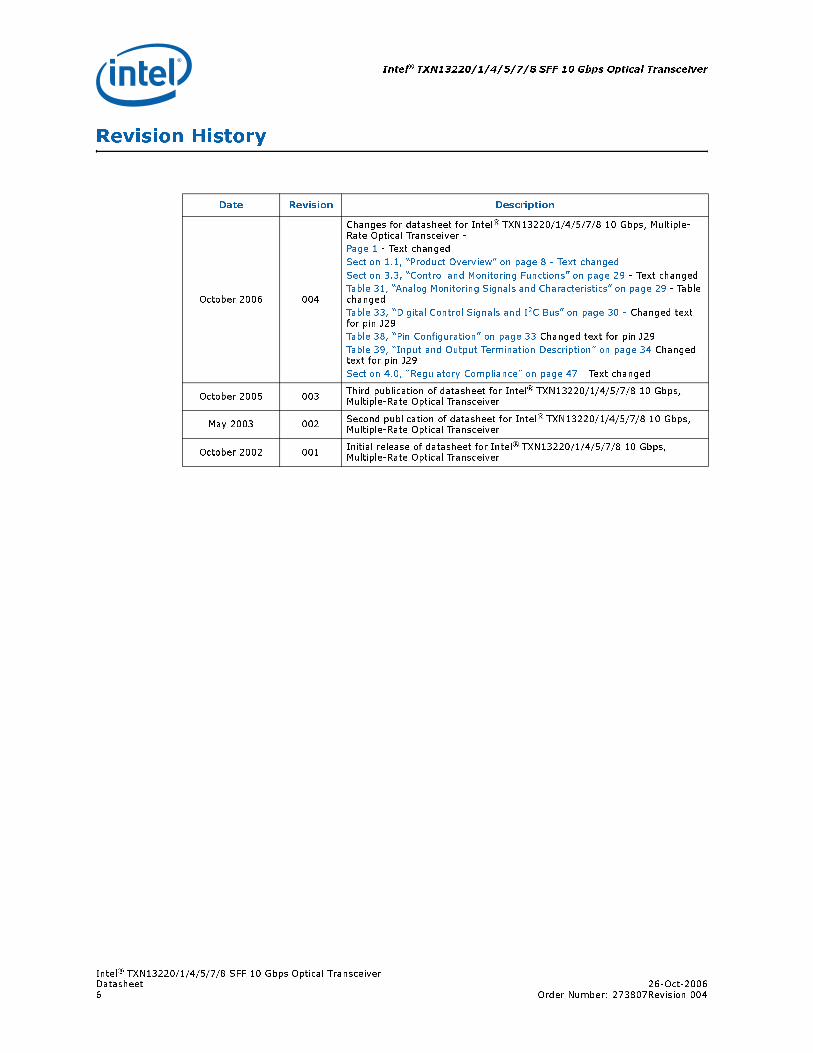
Revision History
Date Revision Description
October 2006 004
Changes for datasheet for Intel® TXN13220/1/4/5/7/8 10 Gbps, Multiple-Rate Optical Transceiver -
Page 1 - Text changed
Section 1.1, “Product Overview” on page 8 - Text changed
Section 3.3, “Control and Monitoring Functions” on page 29 - Text changed
Table 31, “Analog Monitoring Signals and Characteristics” on page 29 - Table changed
Table 33, “Digital Control Signals and I2C Bus” on page 30 - Changed text for pin J29
Table 38, “Pin Configuration” on page 33 Changed text for pin J29
Table 39, “Input and Output Termination Description” on page 34 Changed text for pin J29
Section 4.0, “Regulatory Compliance” on page 47 - Text changed
October 2005 003Third publication of datasheet for Intel® TXN13220/1/4/5/7/8 10 Gbps, Multiple-Rate Optical Transceiver
May 2003 002Second publication of datasheet for Intel® TXN13220/1/4/5/7/8 10 Gbps, Multiple-Rate Optical Transceiver
October 2002 001Initial release of datasheet for Intel® TXN13220/1/4/5/7/8 10 Gbps, Multiple-Rate Optical Transceiver

Intel® TXN13220/1/4/5/7/8 SFF 10 Gbps Optical Transceiver26-Oct-2006 DatasheetOrder Number: 273807, Revision 004 7
Intel® TXN13220/1/4/5/7/8 SFF 10 Gbps Optical Transceiver
Intel® TXN13220/1/4/5/7/8 SFF 10 Gbps Optical Transceiver
Intel® TXN13220/1/4/5/7/8 SFF 10 Gbps Optical TransceiverDatasheet 26-Oct-20068 Order Number: 273807004
1.0 Introduction
This section discusses the following topics:
• Section 1.1, “Product Overview” on page 8
• Section 1.2, “Related Hardware and Documents” on page 10
1.1 Product Overview
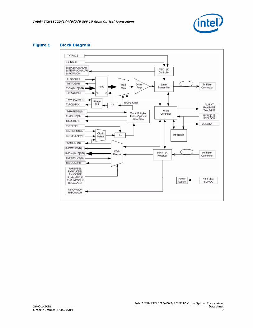
The Intel® TXN13220/7/8 10 Gbps, Multiple-Rate Optical SerDes Transceiver with 16-Channel Multiplexer/Demultiplexer multi-rate line of 10 Gbps SerDes transceivers (called hereafter the TXN13220/1/4/5/7/8 Transceiver) is designed to provide a SONET/SDH, 10 GbE, or FEC interface between the physical layer and the electrical layer. The TXN13220/1/4/5/7/8 Transceiver comprises an optical transmitter and receiver pair, integrated with electrical multiplex and demultiplex functions.
As shown in the Figure 1 block diagram, the TXN13220/1/4/5/7/8 Transceiver transmitter section multiplexes 16 channels from a differential LVDS parallel data bus into a 10 Gbps optical signal launched into a single-mode, optical-fiber pigtail. The transmitter contains a miniature packaged integrated driver with a semi-cooled 1310 nm DFB laser or a cooled 1550 nm EML.
The receiver operates over both the 1.3 µm and 1.5 µm bands and is compliant with SONET/SDH OC-192/STM-64 physical layer specifications and Draft 5.0 of IEEE* 802.3ae 10GBASE-L and 10GBASE-E 10 GbE specifications. The rate at which the TXN13220/1/4/5/7/8 Transceiver operates is digitally selectable. The receiver includes a PIN photodiode and transimpedance amplifier, which operate over both the 1.3 μm and 1.5 μm bands.
The TXN13220/1/4/5/7/8 Transceiver is assembled in a multi-source agreement (MSA) compatible package with dimensions 3.0" L × 2.2" W × 0.53" H. The heatsink was designed for 55 °C ambient temperature/250 linear feet per minute airflow. Alternative heatsink options (for example, 0.63", 0.7" and 0.43” flat top) are also available upon request.
The LVDS interface connection is made using an MSA-compliant, 300-pin, Berg MEG-Array* connector with standard pinout. Optical connections are made with standard SC-UPC or LC-UPC optical connectors. Other optical connection options may be available upon request.
Intel® TXN13220/1/4/5/7/8 SFF 10 Gbps Optical Transceiver26-Oct-2006 DatasheetOrder Number: 273807004 9
Intel® TXN13220/1/4/5/7/8 SFF 10 Gbps Optical Transceiver
Figure 1. Block Diagram
Intel® TXN13220/1/4/5/7/8 SFF 10 Gbps Optical Transceiver
Intel® TXN13220/1/4/5/7/8 SFF 10 Gbps Optical TransceiverDatasheet 26-Oct-200610 Order Number: 273807004
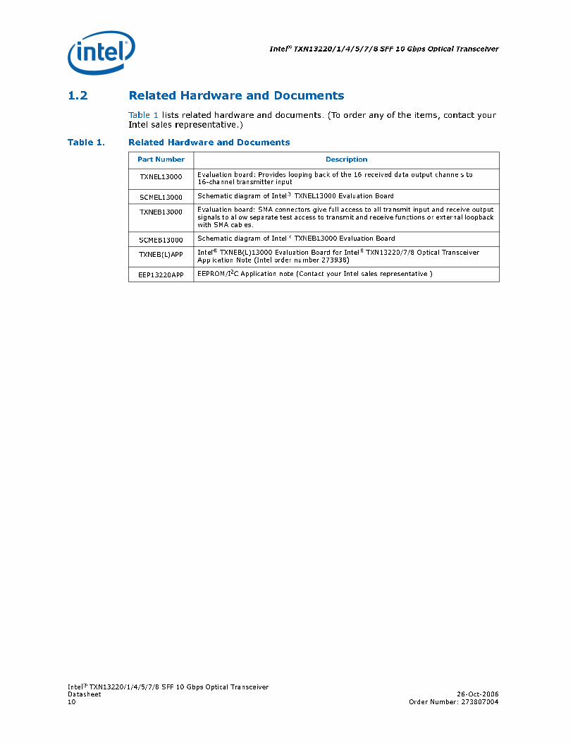
1.2 Related Hardware and Documents
Table 1 lists related hardware and documents. (To order any of the items, contact your Intel sales representative.)
Table 1. Related Hardware and Documents
Part Number Description
TXNEL13000 Evaluation board: Provides looping back of the 16 received data output channels to 16-channel transmitter input
SCMEL13000 Schematic diagram of Intel® TXNEL13000 Evaluation Board
TXNEB13000 Evaluation board: SMA connectors give full access to all transmit input and receive output signals to allow separate test access to transmit and receive functions or external loopback with SMA cables.
SCMEB13000 Schematic diagram of Intel® TXNEB13000 Evaluation Board
TXNEB(L)APP Intel® TXNEB(L)13000 Evaluation Board for Intel® TXN13220/7/8 Optical Transceiver Application Note (Intel order number 273938)
EEP13220APP EEPROM/I2C Application note (Contact your Intel sales representative.)
Intel® TXN13220/1/4/5/7/8 SFF 10 Gbps Optical Transceiver26-Oct-2006 DatasheetOrder Number: 273807004 11
Intel® TXN13220/1/4/5/7/8 SFF 10 Gbps Optical Transceiver
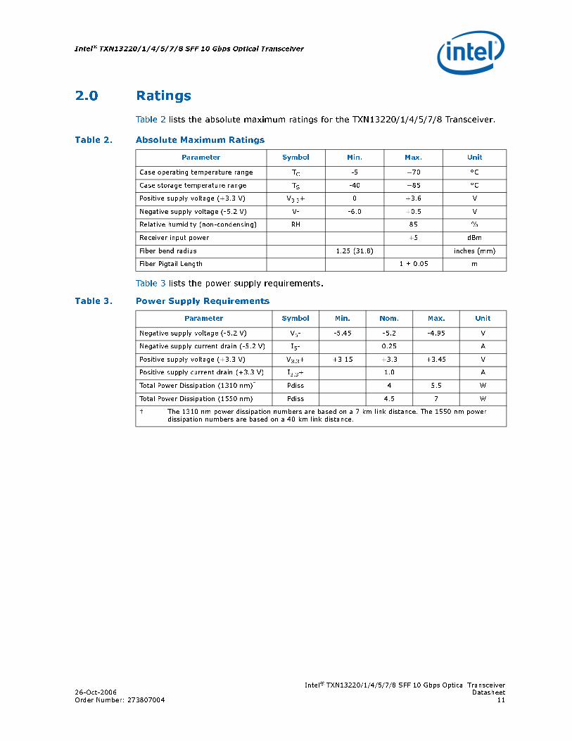
2.0 Ratings
Table 2 lists the absolute maximum ratings for the TXN13220/1/4/5/7/8 Transceiver.
Table 3 lists the power supply requirements.
Table 2. Absolute Maximum Ratings
Parameter Symbol Min. Max. Unit
Case operating temperature range TC -5 +70 °C
Case storage temperature range TS -40 +85 °C
Positive supply voltage (+3.3 V) V3.3+ 0 +3.6 V
Negative supply voltage (-5.2 V) V- -6.0 +0.5 V
Relative humidity (non-condensing) RH 85 %
Receiver input power +5 dBm
Fiber bend radius 1.25 (31.8) inches (mm)
Fiber Pigtail Length 1 ± 0.05 m
Table 3. Power Supply Requirements
Parameter Symbol Min. Nom. Max. Unit
Negative supply voltage (-5.2 V) V5- -5.45 -5.2 -4.95 V
Negative supply current drain (-5.2 V) I5- 0.25 A
Positive supply voltage (+3.3 V) V3.3+ +3.15 +3.3 +3.45 V
Positive supply current drain (+3.3 V) I3.3+ 1.0 A
Total Power Dissipation (1310 nm)† Pdiss 4 5.5 W
Total Power Dissipation (1550 nm)† Pdiss 4.5 7 W
† The 1310 nm power dissipation numbers are based on a 7 km link distance. The 1550 nm power dissipation numbers are based on a 40 km link distance.
Intel® TXN13220/1/4/5/7/8 SFF 10 Gbps Optical Transceiver
Intel® TXN13220/1/4/5/7/8 SFF 10 Gbps Optical TransceiverDatasheet 26-Oct-200612 Order Number: 273807004
3.0 Product Configurations and Specifications
This section discusses the following topics:
• Section 3.1, “Product Configurations” on page 13
• Section 3.2, “Timing” on page 27
• Section 3.3, “Control and Monitoring Functions” on page 29
• Section 3.4, “Data Input/Output Configuration” on page 32
• Section 3.5, “Pin Configuration” on page 33
• Section 3.6, “Input and Output Termination Description” on page 34
• Section 3.7, “Integrated Power Supply Sequencing” on page 43
• Section 3.8, “Mechanical Layout and Configuration” on page 43
Intel® TXN13220/1/4/5/7/8 SFF 10 Gbps Optical Transceiver26-Oct-2006 DatasheetOrder Number: 273807004 13
Intel® TXN13220/1/4/5/7/8 SFF 10 Gbps Optical Transceiver
3.1 Product Configurations
This section discusses the following topics:
• Section 3.1.1, “Summary of Product Configurations” on page 13
• Section 3.1.2, “Intel® TXN132201013 / TXN132251013 Transceivers” on page 15
• Section 3.1.3, “Intel® TXN132271013 / TXN132241013 / TXN132282013 Transceivers” on page 16
• Section 3.1.4, “Intel® TXN132212013 Transceiver” on page 18
• Section 3.1.5, “Intel® TXN132204013 / TXN132274013 Transceiver” on page 20
• Section 3.1.6, “Intel® TXN132203015 / TXN132273015 Transceivers” on page 21
• Section 3.1.7, “Intel® TXN132204015 / TXN132254015 Transceivers” on page 22
• Section 3.1.8, “Intel® TXN132274015 / TXN132244015 / TXN132284015 Transceiver” on page 23
• Section 3.1.9, “Intel® TXN132214015 Transceiver” on page 25
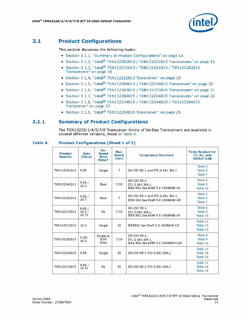
3.1.1 Summary of Product Configurations
The TXN13220/1/4/5/7/8 Transceiver family of SerDes Transceivers are available in several different versions, listed in Table 4.
Table 4. Product Configurations (Sheet 1 of 2)
Product Number
Rate (Gbps)
On-Board Jitter Filter?
Max. Reach (km)
Compliance StandardTable Number for
Tx, Rx, and Optical Link
TXN132201013 9.95 Single 7 GR-253 SR-1 and ITU G.691 I64.1
Table 5
Table 6
Table 7
TXN1322410139.95 / 10.3
Dual 7/10GR-253 SR-1,
ITU G.691 I64.1, IEEE 802.3ae Draft 5.0 10GBASE-LR
Table 8
Table 9
Table 10
TXN1322510139.95 / 10.7
Dual 7GR-253 SR-1 and ITU G.691 I64.1,
IEEE 802.3ae Draft 5.0 10GBASE-LW
Table 5
Table 6
Table 7
TXN1322710139.95 / 10.3 / 10.71
No 7/10GR-253 SR-1,
ITU G.691 I64.1, IEEE 802.3ae Draft 5.0 10GBASE-LR
Table 8
Table 9
Table 10
TXN132212013 10.3 Single 10 IEEE802.3ae Draft 5.0 10GBASE-LR
Table 11
Table 12
Table 13
TXN1322820139.95/10.3
Single at 9.95 Gbps
7/10GR-253 SR-1,
ITU G.691 I64.1, IEEE 802.3ae Draft 5.0 10GBAESE-LR
Table 8
Table 9
Table 10
TXN132203015 9.95 Single 25 GR-253 SR-2 ITU G.691 I64.2
Table 17
Table 18
Table 19
TXN1322730159.95 / 10.71
No 25 GR-253 SR-2 ITU G.691 I64.2
Table 17
Table 18
Table 19
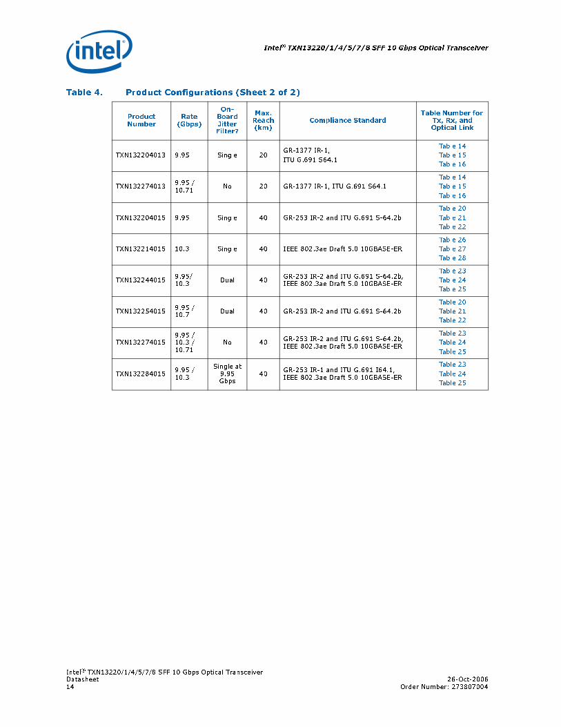
Intel® TXN13220/1/4/5/7/8 SFF 10 Gbps Optical Transceiver
Intel® TXN13220/1/4/5/7/8 SFF 10 Gbps Optical TransceiverDatasheet 26-Oct-200614 Order Number: 273807004
TXN132204013 9.95 Single 20GR-1377 IR-1,
ITU G.691 S64.1
Table 14
Table 15
Table 16
TXN1322740139.95 / 10.71
No 20 GR-1377 IR-1, ITU G.691 S64.1
Table 14
Table 15
Table 16
TXN132204015 9.95 Single 40 GR-253 IR-2 and ITU G.691 S-64.2b
Table 20
Table 21
Table 22
TXN132214015 10.3 Single 40 IEEE 802.3ae Draft 5.0 10GBASE-ER
Table 26
Table 27
Table 28
TXN1322440159.95/10.3
Dual 40GR-253 IR-2 and ITU G.691 S-64.2b, IEEE 802.3ae Draft 5.0 10GBASE-ER
Table 23
Table 24
Table 25
TXN1322540159.95 / 10.7
Dual 40 GR-253 IR-2 and ITU G.691 S-64.2b
Table 20
Table 21
Table 22
TXN1322740159.95 / 10.3 /10.71
No 40GR-253 IR-2 and ITU G.691 S-64.2b,IEEE 802.3ae Draft 5.0 10GBASE-ER
Table 23
Table 24
Table 25
TXN1322840159.95 / 10.3
Single at 9.95 Gbps
40GR-253 IR-1 and ITU G.691 I64.1,IEEE 802.3ae Draft 5.0 10GBASE-ER
Table 23
Table 24
Table 25
Table 4. Product Configurations (Sheet 2 of 2)
Product Number
Rate (Gbps)
On-Board Jitter Filter?
Max. Reach (km)
Compliance StandardTable Number for
Tx, Rx, and Optical Link
Intel® TXN13220/1/4/5/7/8 SFF 10 Gbps Optical Transceiver26-Oct-2006 DatasheetOrder Number: 273807004 15
Intel® TXN13220/1/4/5/7/8 SFF 10 Gbps Optical Transceiver
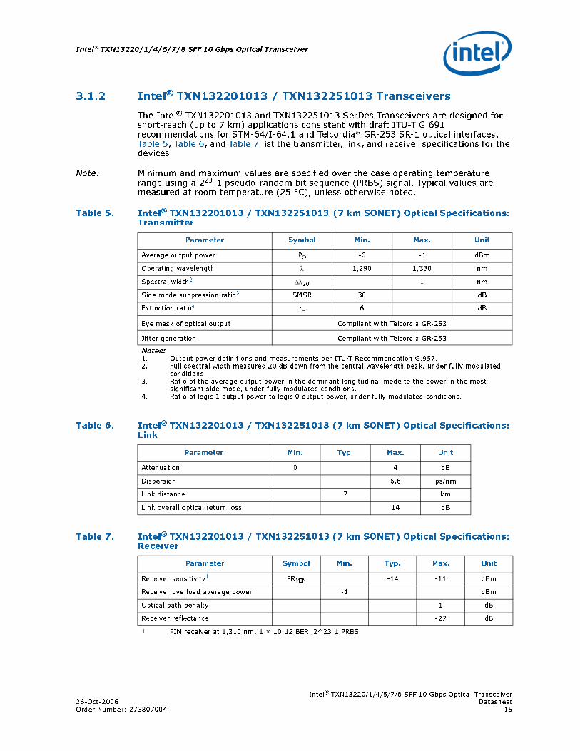
3.1.2 Intel® TXN132201013 / TXN132251013 Transceivers
The Intel® TXN132201013 and TXN132251013 SerDes Transceivers are designed for short-reach (up to 7 km) applications consistent with draft ITU-T G.691 recommendations for STM-64/I-64.1 and Telcordia* GR-253 SR-1 optical interfaces. Table 5, Table 6, and Table 7 list the transmitter, link, and receiver specifications for the devices.
Note: Minimum and maximum values are specified over the case operating temperature range using a 223-1 pseudo-random bit sequence (PRBS) signal. Typical values are measured at room temperature (25 °C), unless otherwise noted.
Table 5. Intel® TXN132201013 / TXN132251013 (7 km SONET) Optical Specifications: Transmitter
Parameter Symbol Min. Max. Unit
Average output power1 PO -6 -1 dBm
Operating wavelength λ 1,290 1,330 nm
Spectral width2 Δλ20 1 nm
Side mode suppression ratio3 SMSR 30 dB
Extinction ratio4 re 6 dB
Eye mask of optical output Compliant with Telcordia GR-253
Jitter generation Compliant with Telcordia GR-253
Notes:1. Output power definitions and measurements per ITU-T Recommendation G.957.2. Full spectral width measured 20 dB down from the central wavelength peak, under fully modulated
conditions.3. Ratio of the average output power in the dominant longitudinal mode to the power in the most
significant side mode, under fully modulated conditions.4. Ratio of logic 1 output power to logic 0 output power, under fully modulated conditions.
Table 6. Intel® TXN132201013 / TXN132251013 (7 km SONET) Optical Specifications: Link
Parameter Min. Typ. Max. Unit
Attenuation 0 4 dB
Dispersion 6.6 ps/nm
Link distance 7 km
Link overall optical return loss 14 dB
Table 7. Intel® TXN132201013 / TXN132251013 (7 km SONET) Optical Specifications: Receiver
Parameter Symbol Min. Typ. Max. Unit
Receiver sensitivity† PRMIN -14 -11 dBm
Receiver overload average power -1 dBm
Optical path penalty 1 dB
Receiver reflectance -27 dB
† PIN receiver at 1,310 nm, 1 × 10-12 BER, 2^23-1 PRBS
Intel® TXN13220/1/4/5/7/8 SFF 10 Gbps Optical Transceiver
Intel® TXN13220/1/4/5/7/8 SFF 10 Gbps Optical TransceiverDatasheet 26-Oct-200616 Order Number: 273807004
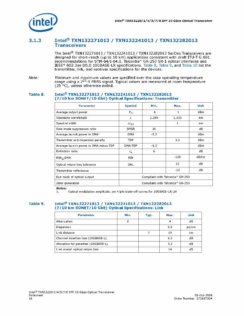
3.1.3 Intel® TXN132271013 / TXN132241013 / TXN132282013 Transceivers
The Intel® TXN132271013 / TXN132241013 / TXN132282013 SerDes Transceivers are designed for short-reach (up to 10 km) applications consistent with draft ITU-T G.691 recommendations for STM-64/I-64.1, Telcordia* GR-253 SR-1 optical interfaces and IEEE* 802.3ae D5.0 10GBASE-LR specifications. Table 8, Table 9, and Table 10 list the transmitter, link, and receiver specifications for the devices.
Note: Minimum and maximum values are specified over the case operating temperature range using a 223-1 PRBS signal. Typical values are measured at room temperature (25 °C), unless otherwise noted.
Table 8. Intel® TXN132271013 / TXN132241013 / TXN132282013 (7/10 km SONET/10 GbE) Optical Specifications: Transmitter
Parameter Symbol Min. Max. Unit
Average output power PO -6 -1 dBm
Operating wavelength λ 1,290 1,330 nm
Spectral width Δλ20 1 nm
Side mode suppression ratio SMSR 30 dB
Average launch power in OMA1 OMA -5.2 dBm
Transmitter and dispersion penalty TDP 3.2 dBm
Average launch power in OMA minus TDP OMA-TDP -6.2 dBm
Extinction ratio re 6 dB
RIN12OMA RIN -128 dB/Hz
Optical return loss tolerance ORL 12 dB
Transmitter reflectance -12 dB
Eye mask of optical output Compliant with Telcordia* GR-253
Jitter generation Compliant with Telcordia* GR-253
Notes:1. Optical modulation amplitude, per triple trade-off curves for 10GBASE-LR/LW
Table 9. Intel® TXN132271013 / TXN132241013 / TXN132282013 (7/10 km SONET/10 GbE) Optical Specifications: Link
Parameter Min. Typ. Max. Unit
Attenuation 0 4 dB
Dispersion 6.6 ps/nm
Link distance 7 10 km
Channel insertion loss (10GBASE-L) 6.2 dB
Allocation for penalties (10GBASE-L) 3.2 dB
Link overall optical return loss 14 dB
Intel® TXN13220/1/4/5/7/8 SFF 10 Gbps Optical Transceiver26-Oct-2006 DatasheetOrder Number: 273807004 17
Intel® TXN13220/1/4/5/7/8 SFF 10 Gbps Optical Transceiver
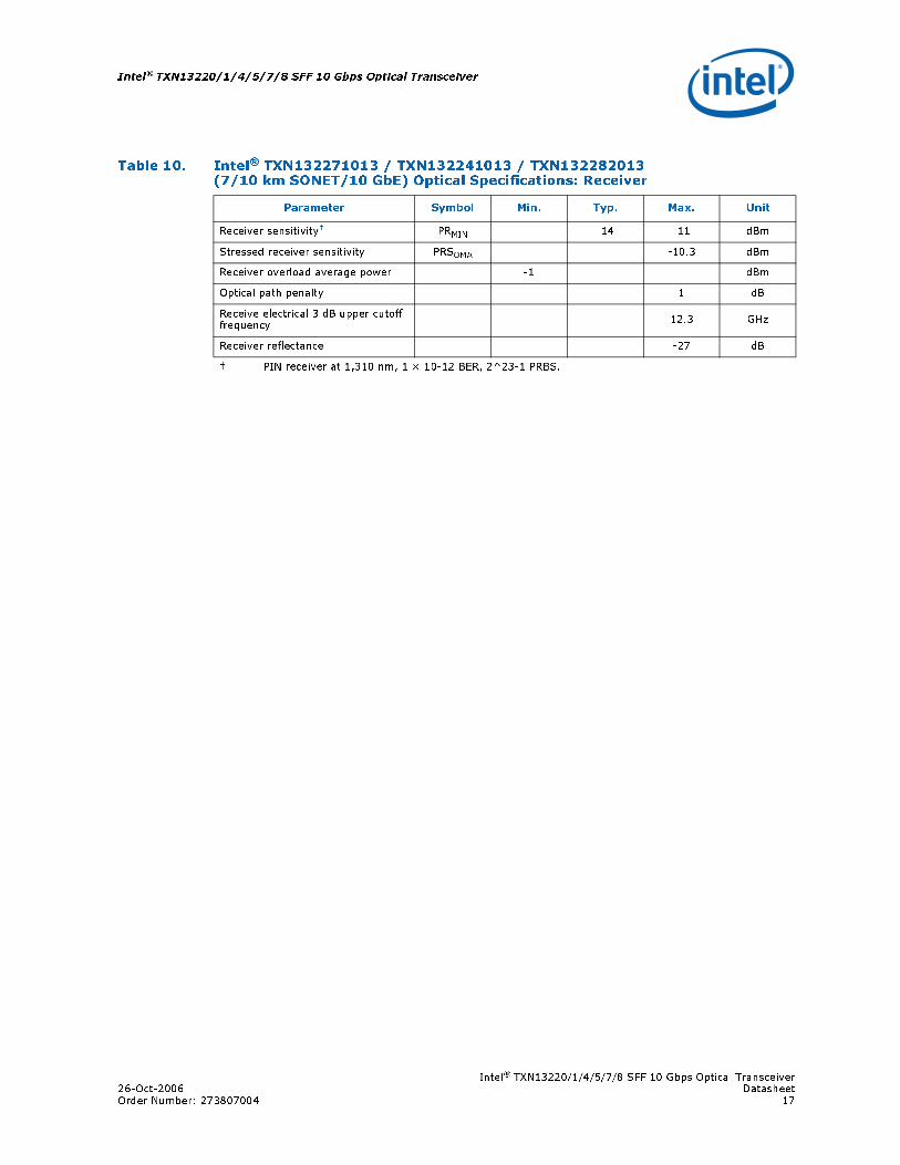
Table 10. Intel® TXN132271013 / TXN132241013 / TXN132282013 (7/10 km SONET/10 GbE) Optical Specifications: Receiver
Parameter Symbol Min. Typ. Max. Unit
Receiver sensitivity† PRMIN -14 -11 dBm
Stressed receiver sensitivity PRSOMA -10.3 dBm
Receiver overload average power -1 dBm
Optical path penalty 1 dB
Receive electrical 3 dB upper cutoff frequency
12.3 GHz
Receiver reflectance -27 dB
† PIN receiver at 1,310 nm, 1 × 10-12 BER, 2^23-1 PRBS.
Intel® TXN13220/1/4/5/7/8 SFF 10 Gbps Optical Transceiver
Intel® TXN13220/1/4/5/7/8 SFF 10 Gbps Optical TransceiverDatasheet 26-Oct-200618 Order Number: 273807004
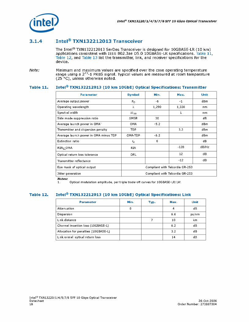
3.1.4 Intel® TXN132212013 Transceiver
The Intel® TXN132212013 SerDes Transceiver is designed for 10GBASE-LR (10 km) applications consistent with IEEE 802.3ae D5.0 10GBASE-LR specifications. Table 11, Table 12, and Table 13 list the transmitter, link, and receiver specifications for the device.
Note: Minimum and maximum values are specified over the case operating temperature range using a 223-1 PRBS signal. Typical values are measured at room temperature (25 °C), unless otherwise noted.
Table 11. Intel® TXN132212013 (10 km 10GbE) Optical Specifications: Transmitter
Parameter Symbol Min. Max. Unit
Average output power PO -6 -1 dBm
Operating wavelength λ 1,290 1,330 nm
Spectral width Δλ20 1 nm
Side mode suppression ratio SMSR 30 dB
Average launch power in OMA1 OMA -5.2 dBm
Transmitter and dispersion penalty TDP 3.2 dBm
Average launch power in OMA minus TDP OMA-TDP -6.2 dBm
Extinction ratio re 6 dB
RIN12OMA RIN -128 dB/Hz
Optical return loss tolerance ORL 12 dB
Transmitter reflectance -12 dB
Eye mask of optical output Compliant with Telcordia GR-253
Jitter generation Compliant with Telcordia GR-253
Notes:1. Optical modulation amplitude, per triple trade-off curves for 10GBASE-LR/LW.
Table 12. Intel® TXN132212013 (10 km 10GbE) Optical Specifications: Link
Parameter Min. Typ. Max. Unit
Attenuation 0 4 dB
Dispersion 6.6 ps/nm
Link distance 7 10 km
Channel insertion loss (10GBASE-L) 6.2 dB
Allocation for penalties (10GBASE-L) 3.2 dB
Link overall optical return loss 14 dB
Intel® TXN13220/1/4/5/7/8 SFF 10 Gbps Optical Transceiver26-Oct-2006 DatasheetOrder Number: 273807004 19
Intel® TXN13220/1/4/5/7/8 SFF 10 Gbps Optical Transceiver
Table 13. Intel® TXN132212013 (10 km 10GbE) Optical Specifications: Receiver
Parameter Symbol Min. Typ. Max. Unit
Receiver sensitivity† PRMIN -14 -11 dBm
Stressed receiver sensitivity PRSOMA -10.3 dBm
Receiver overload average power -1 dBm
Optical path penalty 1 dB
Receive electrical 3 dB upper cutoff frequency 12.3 GHz
Receiver reflectance -27 dB
† PIN receiver at 1,310 nm, 1 × 10-12 BER, 2^23-1 PRBS.
Intel® TXN13220/1/4/5/7/8 SFF 10 Gbps Optical Transceiver
Intel® TXN13220/1/4/5/7/8 SFF 10 Gbps Optical TransceiverDatasheet 26-Oct-200620 Order Number: 273807004
3.1.5 Intel® TXN132204013 / TXN132274013 Transceiver
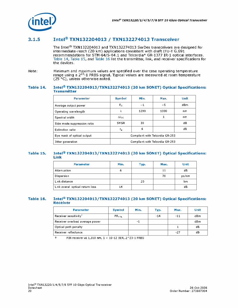
The Intel® TXN132204013 and TXN132274013 SerDes transceivers are designed for intermediate-reach (20 km) applications consistent with draft ITU-T G.691 recommendations for STM-64/S-64.1 and Telcordia* GR-1377 IR-1 optical interfaces. Table 14, Table 15, and Table 16 list the transmitter, link, and receiver specifications for the devices.
Note: Minimum and maximum values are specified over the case operating temperature range using a 223-1 PRBS signal. Typical values are measured at room temperature (25 °C), unless otherwise noted.
Table 14. Intel® TXN132204013/TXN132274013 (20 km SONET) Optical Specifications:Transmitter
Parameter Symbol Min. Max. Unit
Average output power PO +1 +5 dBm
Operating wavelength λ 1290 1330 nm
Spectral width Δλ20 1 nm
Side mode suppression ratio SMSR 30 dB
Extinction ratio re 6 dB
Eye mask of optical output Compliant with Telcordia GR-253
Jitter generation Compliant with Telcordia GR-253
Table 15. Intel® TXN132204013/TXN132274013 (20 km SONET) Optical Specifications:Link
Parameter Min. Typ. Max. Unit
Attenuation 6 11 dB
Dispersion 70 ps/nm
Link distance 20 km
Link overall optical return loss 14 dB
Table 16. Intel® TXN132204013/TXN132274013 (20 km SONET) Optical Specifications:Receiver
Parameter Symbol Min. Typ. Max. Unit
Receiver sensitivity† PRMIN -14 -11 dBm
Receiver overload average power -1 dBm
Optical path penalty 1 dB
Receiver reflectance -27 dB
† PIN receiver at 1,310 nm, 1 × 10-12 BER, 2^23-1 PRBS.
Intel® TXN13220/1/4/5/7/8 SFF 10 Gbps Optical Transceiver26-Oct-2006 DatasheetOrder Number: 273807004 21
Intel® TXN13220/1/4/5/7/8 SFF 10 Gbps Optical Transceiver
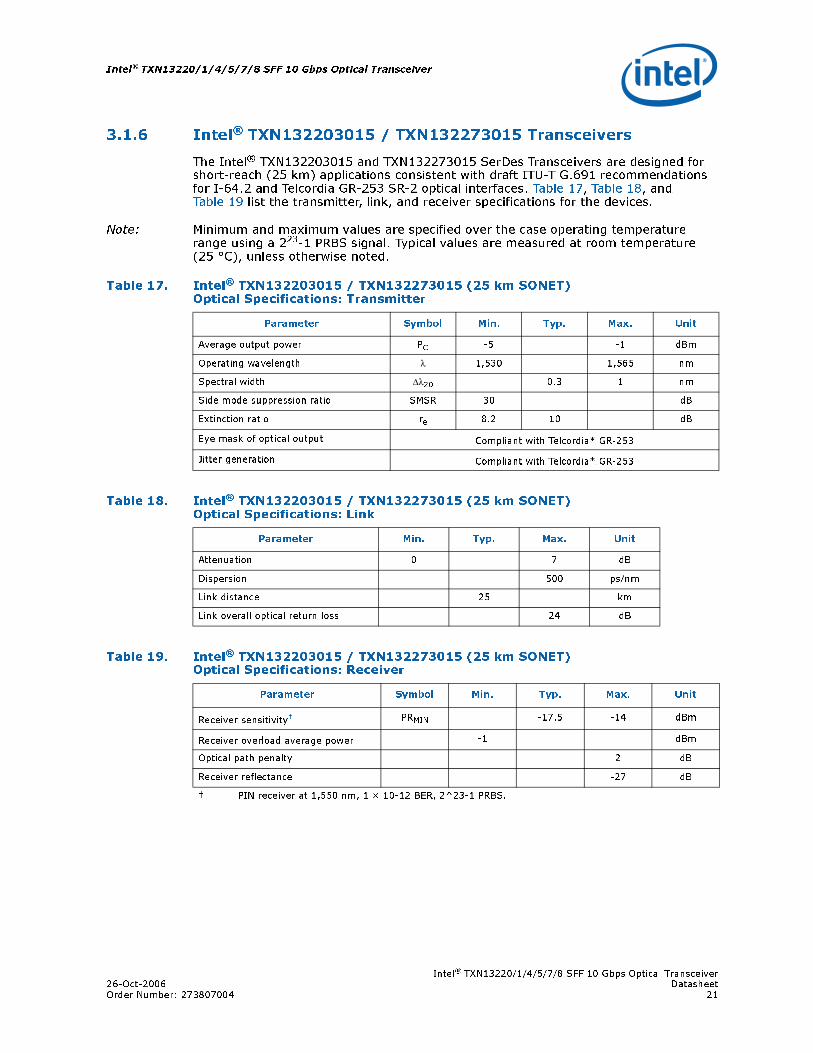
3.1.6 Intel® TXN132203015 / TXN132273015 Transceivers
The Intel® TXN132203015 and TXN132273015 SerDes Transceivers are designed for short-reach (25 km) applications consistent with draft ITU-T G.691 recommendations for I-64.2 and Telcordia GR-253 SR-2 optical interfaces. Table 17, Table 18, and Table 19 list the transmitter, link, and receiver specifications for the devices.
Note: Minimum and maximum values are specified over the case operating temperature range using a 223-1 PRBS signal. Typical values are measured at room temperature (25 °C), unless otherwise noted.
Table 17. Intel® TXN132203015 / TXN132273015 (25 km SONET) Optical Specifications: Transmitter
Parameter Symbol Min. Typ. Max. Unit
Average output power PO -5 -1 dBm
Operating wavelength λ 1,530 1,565 nm
Spectral width Δλ20 0.3 1 nm
Side mode suppression ratio SMSR 30 dB
Extinction ratio re 8.2 10 dB
Eye mask of optical output Compliant with Telcordia* GR-253
Jitter generation Compliant with Telcordia* GR-253
Table 18. Intel® TXN132203015 / TXN132273015 (25 km SONET) Optical Specifications: Link
Parameter Min. Typ. Max. Unit
Attenuation 0 7 dB
Dispersion 500 ps/nm
Link distance 25 km
Link overall optical return loss 24 dB
Table 19. Intel® TXN132203015 / TXN132273015 (25 km SONET) Optical Specifications: Receiver
Parameter Symbol Min. Typ. Max. Unit
Receiver sensitivity† PRMIN -17.5 -14 dBm
Receiver overload average power -1 dBm
Optical path penalty 2 dB
Receiver reflectance -27 dB
† PIN receiver at 1,550 nm, 1 × 10-12 BER, 2^23-1 PRBS.
Intel® TXN13220/1/4/5/7/8 SFF 10 Gbps Optical Transceiver
Intel® TXN13220/1/4/5/7/8 SFF 10 Gbps Optical TransceiverDatasheet 26-Oct-200622 Order Number: 273807004
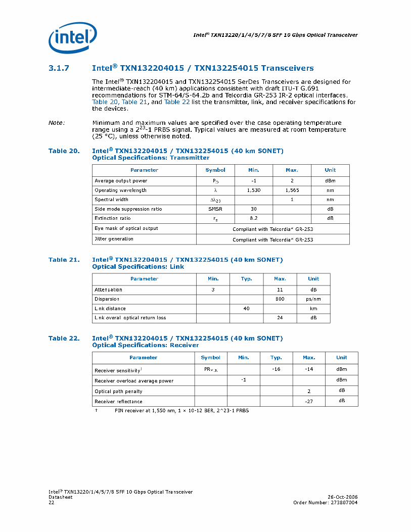
3.1.7 Intel® TXN132204015 / TXN132254015 Transceivers
The Intel® TXN132204015 and TXN132254015 SerDes Transceivers are designed for intermediate-reach (40 km) applications consistent with draft ITU-T G.691 recommendations for STM-64/S-64.2b and Telcordia GR-253 IR-2 optical interfaces. Table 20, Table 21, and Table 22 list the transmitter, link, and receiver specifications for the devices.
Note: Minimum and maximum values are specified over the case operating temperature range using a 223-1 PRBS signal. Typical values are measured at room temperature (25 °C), unless otherwise noted.
Table 20. Intel® TXN132204015 / TXN132254015 (40 km SONET) Optical Specifications: Transmitter
Parameter Symbol Min. Max. Unit
Average output power PO -1 2 dBm
Operating wavelength λ 1,530 1,565 nm
Spectral width Δλ20 1 nm
Side mode suppression ratio SMSR 30 dB
Extinction ratio re 8.2 dB
Eye mask of optical output Compliant with Telcordia* GR-253
Jitter generation Compliant with Telcordia* GR-253
Table 21. Intel® TXN132204015 / TXN132254015 (40 km SONET) Optical Specifications: Link
Parameter Min. Typ. Max. Unit
Attenuation 3 11 dB
Dispersion 800 ps/nm
Link distance 40 km
Link overall optical return loss 24 dB
Table 22. Intel® TXN132204015 / TXN132254015 (40 km SONET) Optical Specifications: Receiver
Parameter Symbol Min. Typ. Max. Unit
Receiver sensitivity† PRMIN -16 -14 dBm
Receiver overload average power -1 dBm
Optical path penalty 2 dB
Receiver reflectance -27 dB
† PIN receiver at 1,550 nm, 1 × 10-12 BER, 2^23-1 PRBS.
Intel® TXN13220/1/4/5/7/8 SFF 10 Gbps Optical Transceiver26-Oct-2006 DatasheetOrder Number: 273807004 23
Intel® TXN13220/1/4/5/7/8 SFF 10 Gbps Optical Transceiver
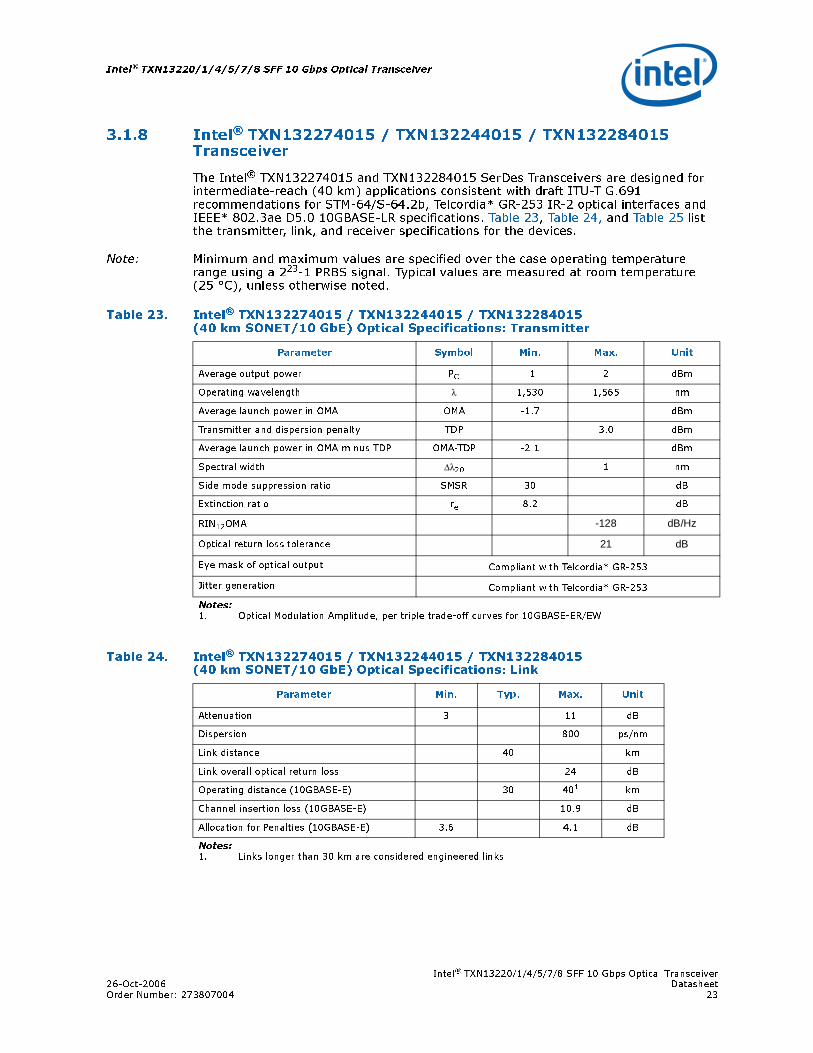
3.1.8 Intel® TXN132274015 / TXN132244015 / TXN132284015 Transceiver
The Intel® TXN132274015 and TXN132284015 SerDes Transceivers are designed for intermediate-reach (40 km) applications consistent with draft ITU-T G.691 recommendations for STM-64/S-64.2b, Telcordia* GR-253 IR-2 optical interfaces and IEEE* 802.3ae D5.0 10GBASE-LR specifications. Table 23, Table 24, and Table 25 list the transmitter, link, and receiver specifications for the devices.
Note: Minimum and maximum values are specified over the case operating temperature range using a 223-1 PRBS signal. Typical values are measured at room temperature (25 °C), unless otherwise noted.
Table 23. Intel® TXN132274015 / TXN132244015 / TXN132284015 (40 km SONET/10 GbE) Optical Specifications: Transmitter
Parameter Symbol Min. Max. Unit
Average output power PO -1 2 dBm
Operating wavelength λ 1,530 1,565 nm
Average launch power in OMA OMA -1.7 dBm
Transmitter and dispersion penalty TDP 3.0 dBm
Average launch power in OMA minus TDP OMA-TDP -2.1 dBm
Spectral width Δλ20 1 nm
Side mode suppression ratio SMSR 30 dB
Extinction ratio re 8.2 dB
RIN12OMA -128 dB/Hz
Optical return loss tolerance 21 dB
Eye mask of optical output Compliant with Telcordia* GR-253
Jitter generation Compliant with Telcordia* GR-253
Notes: 1. Optical Modulation Amplitude, per triple trade-off curves for 10GBASE-ER/EW
Table 24. Intel® TXN132274015 / TXN132244015 / TXN132284015 (40 km SONET/10 GbE) Optical Specifications: Link
Parameter Min. Typ. Max. Unit
Attenuation 3 11 dB
Dispersion 800 ps/nm
Link distance 40 km
Link overall optical return loss 24 dB
Operating distance (10GBASE-E) 30 401 km
Channel insertion loss (10GBASE-E) 10.9 dB
Allocation for Penalties (10GBASE-E) 3.6 4.1 dB
Notes: 1. Links longer than 30 km are considered engineered links
Intel® TXN13220/1/4/5/7/8 SFF 10 Gbps Optical Transceiver
Intel® TXN13220/1/4/5/7/8 SFF 10 Gbps Optical TransceiverDatasheet 26-Oct-200624 Order Number: 273807004
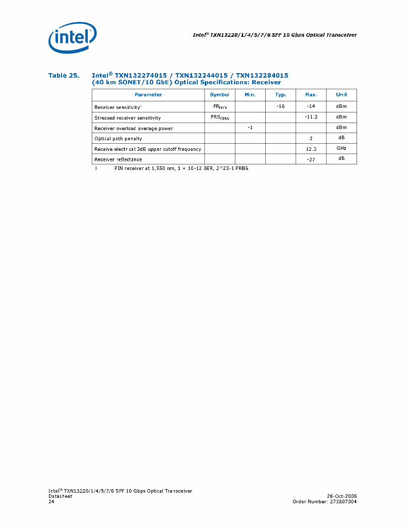
Table 25. Intel® TXN132274015 / TXN132244015 / TXN132284015(40 km SONET/10 GbE) Optical Specifications: Receiver
Parameter Symbol Min. Typ. Max. Unit
Receiver sensitivity† PRMIN -16 -14 dBm
Stressed receiver sensitivity PRSOMA -11.3 dBm
Receiver overload average power -1 dBm
Optical path penalty 2 dB
Receive electrical 3dB upper cutoff frequency 12.3 GHz
Receiver reflectance -27 dB
† PIN receiver at 1,550 nm, 1 × 10-12 BER, 2^23-1 PRBS.
Intel® TXN13220/1/4/5/7/8 SFF 10 Gbps Optical Transceiver26-Oct-2006 DatasheetOrder Number: 273807004 25
Intel® TXN13220/1/4/5/7/8 SFF 10 Gbps Optical Transceiver
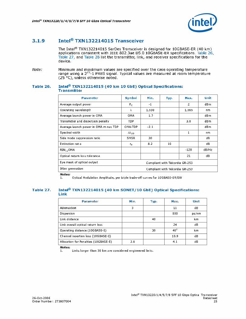
3.1.9 Intel® TXN132214015 Transceiver
The Intel® TXN132214015 SerDes Transceiver is designed for 10GBASE-ER (40 km) applications consistent with IEEE 802.3ae D5.0 10GBASE-ER specifications. Table 26, Table 27, and Table 28 list the transmitter, link, and receiver specifications for the device.
Note: Minimum and maximum values are specified over the case operating temperature range using a 223-1 PRBS signal. Typical values are measured at room temperature (25 °C), unless otherwise noted.
Table 26. Intel® TXN132214015 (40 km 10 GbE) Optical Specifications: Transmitter
Parameter Symbol Min. Typ. Max. Unit
Average output power PO -1 2 dBm
Operating wavelength λ 1,530 1,565 nm
Average launch power in OMA OMA -1.7 dBm
Transmitter and dispersion penalty TDP 3.0 dBm
Average launch power in OMA minus TDP OMA-TDP -2.1 dBm
Spectral width Δλ20 1 nm
Side mode suppression ratio SMSR 30 dB
Extinction ratio re 8.2 10 dB
RIN12OMA -128 dB/Hz
Optical return loss tolerance 21 dB
Eye mask of optical output Compliant with Telcordia GR-253
Jitter generation Compliant with Telcordia GR-253
Notes: 1. Optical Modulation Amplitude, per triple trade-off curves for 10GBASE-ER/EW
Table 27. Intel® TXN132214015 (40 km SONET/10 GbE) Optical Specifications: Link
Parameter Min. Typ. Max. Unit
Attenuation 3 11 dB
Dispersion 800 ps/nm
Link distance 40 km
Link overall optical return loss 24 dB
Operating distance (10GBASE-E) 30 401 km
Channel insertion loss (10GBASE-E) 10.9 dB
Allocation for Penalties (10GBASE-E) 3.6 4.1 dB
Notes: 1. Links longer than 30 km are considered engineered links.
Intel® TXN13220/1/4/5/7/8 SFF 10 Gbps Optical Transceiver
Intel® TXN13220/1/4/5/7/8 SFF 10 Gbps Optical TransceiverDatasheet 26-Oct-200626 Order Number: 273807004
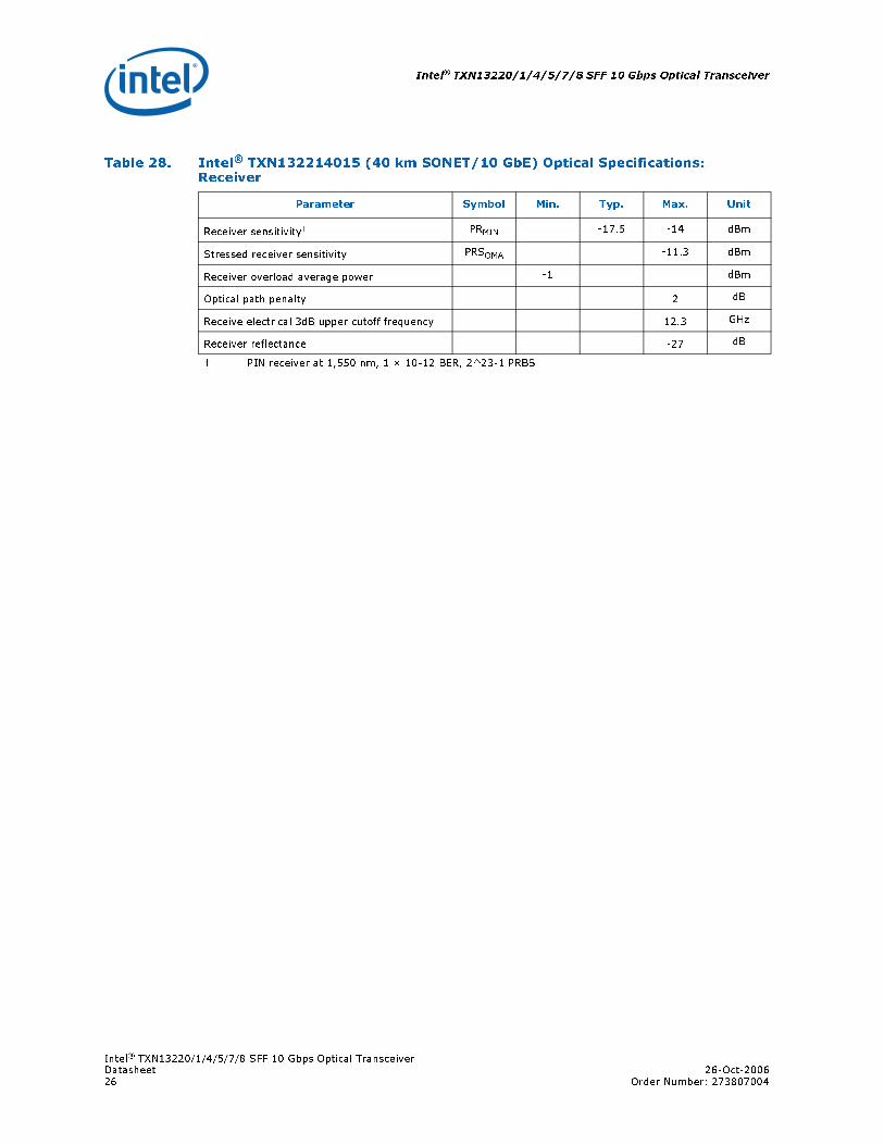
Table 28. Intel® TXN132214015 (40 km SONET/10 GbE) Optical Specifications: Receiver
Parameter Symbol Min. Typ. Max. Unit
Receiver sensitivity† PRMIN -17.5 -14 dBm
Stressed receiver sensitivity PRSOMA -11.3 dBm
Receiver overload average power -1 dBm
Optical path penalty 2 dB
Receive electrical 3dB upper cutoff frequency 12.3 GHz
Receiver reflectance -27 dB
† PIN receiver at 1,550 nm, 1 × 10-12 BER, 2^23-1 PRBS.
Intel® TXN13220/1/4/5/7/8 SFF 10 Gbps Optical Transceiver26-Oct-2006 DatasheetOrder Number: 273807004 27
Intel® TXN13220/1/4/5/7/8 SFF 10 Gbps Optical Transceiver
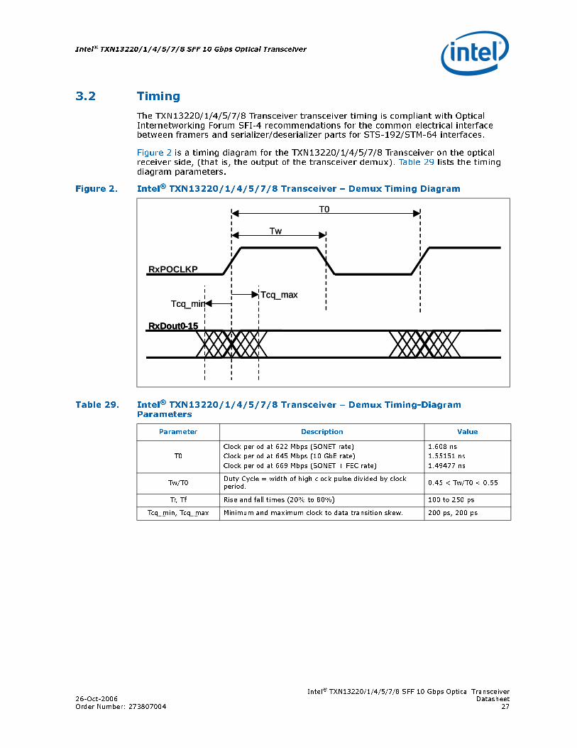
3.2 Timing
The TXN13220/1/4/5/7/8 Transceiver transceiver timing is compliant with Optical Internetworking Forum SFI-4 recommendations for the common electrical interface between framers and serializer/deserializer parts for STS-192/STM-64 interfaces.
Figure 2 is a timing diagram for the TXN13220/1/4/5/7/8 Transceiver on the optical receiver side, (that is, the output of the transceiver demux). Table 29 lists the timing diagram parameters.
Figure 2. Intel® TXN13220/1/4/5/7/8 Transceiver – Demux Timing Diagram
Table 29. Intel® TXN13220/1/4/5/7/8 Transceiver – Demux Timing-Diagram Parameters
Parameter Description Value
T0
Clock period at 622 Mbps (SONET rate)
Clock period at 645 Mbps (10 GbE rate)
Clock period at 669 Mbps (SONET + FEC rate)
1.608 ns
1.55151 ns
1.49477 ns
Tw/T0Duty Cycle = width of high clock pulse divided by clock period.
0.45 < Tw/T0 < 0.55
Tr, Tf Rise and fall times (20% to 80%) 100 to 250 ps
Tcq_min, Tcq_max Minimum and maximum clock to data transition skew. 200 ps, 200 ps
Tcq_min Tcq_max
Tw
T0
RxDout0 - 15
RxPOCLKP
Tcq_min Tcq_max
Tw
T0
RxDout0 - 15 RxDout0 - 15
Intel® TXN13220/1/4/5/7/8 SFF 10 Gbps Optical Transceiver
Intel® TXN13220/1/4/5/7/8 SFF 10 Gbps Optical TransceiverDatasheet 26-Oct-200628 Order Number: 273807004
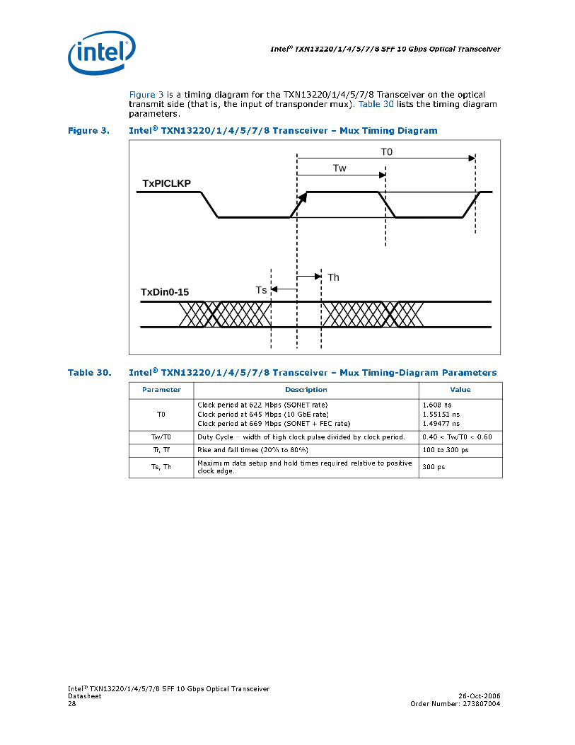
Figure 3 is a timing diagram for the TXN13220/1/4/5/7/8 Transceiver on the optical transmit side (that is, the input of transponder mux). Table 30 lists the timing diagram parameters.
Figure 3. Intel® TXN13220/1/4/5/7/8 Transceiver – Mux Timing Diagram
Table 30. Intel® TXN13220/1/4/5/7/8 Transceiver – Mux Timing-Diagram Parameters
Parameter Description Value
T0
Clock period at 622 Mbps (SONET rate)
Clock period at 645 Mbps (10 GbE rate)
Clock period at 669 Mbps (SONET + FEC rate)
1.608 ns
1.55151 ns
1.49477 ns
Tw/T0 Duty Cycle = width of high clock pulse divided by clock period. 0.40 < Tw/T0 < 0.60
Tr, Tf Rise and fall times (20% to 80%) 100 to 300 ps
Ts, ThMaximum data setup and hold times required relative to positive clock edge.
300 ps
Tw
T0
Th Ts
TxPICLKP
TxDin0-15
Intel® TXN13220/1/4/5/7/8 SFF 10 Gbps Optical Transceiver26-Oct-2006 DatasheetOrder Number: 273807004 29
Intel® TXN13220/1/4/5/7/8 SFF 10 Gbps Optical Transceiver
3.3 Control and Monitoring Functions
The TXN13220/1/4/5/7/8 Transceiver line of transceivers provides a combination of analog and digital control and monitoring functions as listed in Table 31, Table 32, and Table 33.
Note:
• Active signal monitoring using an on-board microprocessor through the I2C bus is available for this optical transceiver. For more information, consult the EEP13220APP application note.
• A fixed content EEPROM, containing many transceiver parameters (for example, calibration data and serial number), can also be accessed through the I2C bus by using a different address. For details, see the EEP13220APP document referenced in Section 1.2, “Related Hardware and Documents” on page 10.
Table 31. Analog Monitoring Signals and Characteristics
Function Pin NamePin
NumberSignal Range
Input optical power
RxPOWMON F3
Output voltage proportional to average received optical power
Referenced to 0 V with typical slope of 1 V/mW (minimum 0.8V/mW and maximum 1.26 V/mW)
Voltage – 0 to 2 V
Current – ± 100 µA
Laser bias monitor
LsBIASMON F18
Output proportional to transmit laser DC bias
V = 20 * (I – Offset) mV where I = laser bias mA.
Voltage – 0 to 2 V
Current – ± 100 µA
Laser temperature monitor
LsTEMPMON D21
Output proportional to transmit laser temperature
V = 0.764*e3887*(1/T – 1/298) volts, where T is temperature in Kelvins.
Nominally 0.4 to 0.6 V under normal operation.
Voltage – 0 to 3.3 V
Current – ±100 µA
Laser power monitor
LsPOWMON D18
Output proportional to transmit laser average output power.
Nominal value of 0.5 V should remain constant due to high gain power control loop.
Voltage – 0 to 2 V
Current – ± 100 µA
Intel® TXN13220/1/4/5/7/8 SFF 10 Gbps Optical Transceiver
Intel® TXN13220/1/4/5/7/8 SFF 10 Gbps Optical TransceiverDatasheet 26-Oct-200630 Order Number: 273807004
Table 32. Digital Alarms
Function Pin NamePin
Num-ber
Logic Logic 0 Logic 1 Condition
Transmitter PLL lock error
TxLOCKERR B30 LVTTLOut of lock
In lockOut of lock when on chip VCO not locked to TxREFCLK
Receiver PLL lock detect
RxLOCKERR B15 LVTTLOut of lock
In lockLow if CDR is unable to recover valid clock from receive optical input signal.
Receiver loss of average power alarm
RxPOWALM F6 LVTTLNo input signal
Input signal present
Logic high for signal above receiver sensitivity. Low for signal < -30 dBm.
Laser bias alarm
LsBIASALM F24 LVTTL Alarm Normal Alarm if laser bias >100 mA
Laser temp alarm
LsTEMPALM F27 LVTTL Alarm NormalAlarm if laser temperature deviates more than 2.5 degrees from initial set point
Receiver alarm interrupt
RxALMINT J14 LVTTL Alarm Normal Electrical OR of all receive alarms
Alarm interrupt ALMINT H15 LVTTL Alarm NormalElectrical OR of all receive and transmit alarms
Transmitter alarm interrupt
TxALMINT J16 LVTTL Alarm Normal Electrical OR of all transmit alarms
Table 33. Digital Control Signals and I2C Bus
Function Pin NamePin
Num-ber
Logic Logic 0 Logic 1
Transmitter laser enable in LsENABLE F21 LVTTL Enabled Disabled
Selects 1/64 line bit rate or 1/16 line bit rate-MHz reference clock for mux - TxREFCLK
TxREFSEL F30 LVTTL1/64 line bit
rate MHz1/16 line bit
rate MHz
Selects 1/64 line bit rate or 1/16 line bit rate of reference clock for demux - RxREFCLK
RxREFSEL F15 LVTTL1/64 line bit
rate1/16 line bit
rate
Selects 1/64 line bit rate or 1/16 line bit rate of demux monitor clock out - RxMCLK
RxMCLKSEL B12 LVTTL1/64 line bit
rate1/16 line bit
rate
Line timing mode internally loops recovered receive clock (RxPOCLK) back to TxREFCLK
TxLINETIMSEL H30 LVTTL Line TimingTxREFCLK
Timing
Receive lock to reference forces the VCO in the receiver clock recovery circuit to lock to RxREFCLK
RxLCKREF B9 LVTTL Lock to ref Normal
Mutes the data outputs of the demux RxMuteDout B6 LVTTLMutes the RxDout [0:15]
Normal
Mutes the RxPOCLK RxMutePOCLK K9 LVTTLMutes the RxPOCLK
Normal
I2C Clock Input I2CCLOCK K15 LVTTL
I2C Data† I2CDATA K18 LVTTL
TxRATESEL1 TxRateSel1 J21 LVTTL See Table 34 See Table 34
TxRATESEL0 TxRateSel0 K21 LVTTL See Table 34 See Table 34
† See the application note for details regarding the contents of the EEPROM.
Intel® TXN13220/1/4/5/7/8 SFF 10 Gbps Optical Transceiver26-Oct-2006 DatasheetOrder Number: 273807004 31
Intel® TXN13220/1/4/5/7/8 SFF 10 Gbps Optical Transceiver
Table 34. Truth Table for Transmit Rate Select (TxRATESEL[0:1])
TxRATESEL1 TxRATESEL0 Rate Selected
0 0 10 GbE rate of 10.3 Gbps selected
0 1 Jitter-filter disable/enable from default
1 0 FEC rate of 10.7 Gbps selected
1 1 SONET rate of 9.85 Gbps selected
Table 35. Deserializer Logic Levels
SymbolLVDS/LVTTL
Characteristic Min. Typ. Max. Units
|Vod| LVDS LVDS output differential voltage 400 mV
Vocm LVDS LVDS output common mode voltage 1.2 V
Vih LVTTL LVTTL input high voltage 2 5 V
Iih LVTTL Input high current -500 0 µA
Vil LVTTL Input low voltage 0 0.8 V
Iil LVTTL Input low current 0 400 µA
Table 36. Serializer Logic Levels
SymbolLVDS/LVTTL
Characteristic Min. Typ. Max. Units
|Vod| LVDS LVDS output differential voltage 400 mV
Vocm LVDS LVDS output common mode voltage 1.2 V
Vivr LVDS LVDS input voltage range 0.8 2.4 V
Rin LVDS LVDS input termination resistor 80 100 120 Ω
Vih LVTTL LVDS input high voltage 2 5 V
Iih LVTTL Input high current -500 0 µA
Vil LVTTL Input high voltage 0 0.8 V
Iil LVTTL Input low current 0 400 µA
Voh LVTTL LVTTL output voltage high 2.4 V
Vol LVTTL Output voltage low 0.4 V
Intel® TXN13220/1/4/5/7/8 SFF 10 Gbps Optical Transceiver
Intel® TXN13220/1/4/5/7/8 SFF 10 Gbps Optical TransceiverDatasheet 26-Oct-200632 Order Number: 273807004
3.4 Data Input/Output Configuration
The TXN13220/1/4/5/7/8 Transceiver product line of transceivers fully compliant with OIF standards for LVDS I/O data format.
Bit ordering is compliant with SONET requirements, whereby the most-significant bit is transmitted first. SONET bit ordering is maintained for all data rates.
Table 37 lists the I/O configuration.
Table 37. Data Input/Output Configuration
Pin NameIn/Out
Description Logic
TxDin0P(N), …, TxDin15P(N)
InTransmitter (1/16 line bit rate) data input, differential pairs.
LVDS, internally 100 Ω terminated
TxPICLKP(N) InTransmitter (1/16 line bit rate) input clock, differential pair, aligned with input data
LVDS, internally 100 Ω terminated
TxREFCLKP(N) InTransmitter reference clock input, differential pair. Selectable between 1/64 line bit rate and 1/16 line bit rate MHz using TxREFSEL
LVPECL, AC Coupled
TxPCLKP(N) OutTransmitter (1/16 line bit rate) reference clock output, differential pair
LVDS
RxDout0P(N), …, RxDout15P(N)
OutReceiver (1/16 line bit rate) data output, differential pairs
LVDS
RxREFCLKP(N) InReceiver reference clock input, differential pair. Selectable between 1/64 line bit rate and 1/16 line bit rate MHz using RxREFSEL
LVPECL, AC Coupled
RxPOCLKP(N) OutReceiver (1/16 line bit rate) MHz clock output, differential pairs, aligned with output data
LVDS
RxMCLKP(N) OutDemultiplexer monitor clock output. Selectable between 1/64 line bit rate and 1/16 line bit rate MHz by using RxMCLKSEL
LVDS
TxMCLKP(N) OutMultiplexer monitor clock output: 1/64 line bit rate MHz
LVDS
Intel® TXN13220/1/4/5/7/8 SFF 10 Gbps Optical Transceiver26-Oct-2006 DatasheetOrder Number: 273807004 33
Intel® TXN13220/1/4/5/7/8 SFF 10 Gbps Optical Transceiver
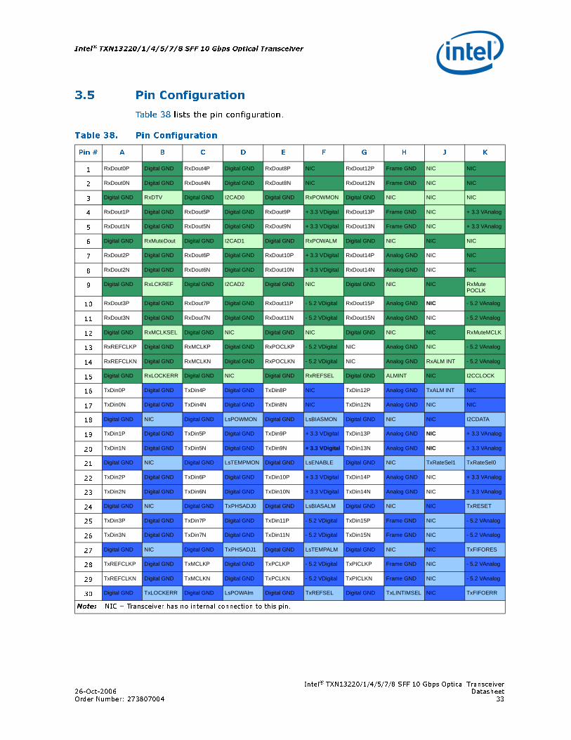
3.5 Pin Configuration
Table 38 lists the pin configuration.
Table 38. Pin Configuration
Pin # A B C D E F G H J K
1 RxDout0P Digital GND RxDout4P Digital GND RxDout8P NIC RxDout12P Frame GND NIC NIC
2 RxDout0N Digital GND RxDout4N Digital GND RxDout8N NIC RxDout12N Frame GND NIC NIC
3 Digital GND RxDTV Digital GND I2CAD0 Digital GND RxPOWMON Digital GND NIC NIC NIC
4 RxDout1P Digital GND RxDout5P Digital GND RxDout9P + 3.3 VDigital RxDout13P Frame GND NIC + 3.3 VAnalog
5 RxDout1N Digital GND RxDout5N Digital GND RxDout9N + 3.3 VDigital RxDout13N Frame GND NIC + 3.3 VAnalog
6 Digital GND RxMuteDout Digital GND I2CAD1 Digital GND RxPOWALM Digital GND NIC NIC NIC
7 RxDout2P Digital GND RxDout6P Digital GND RxDout10P + 3.3 VDigital RxDout14P Analog GND NIC NIC
8 RxDout2N Digital GND RxDout6N Digital GND RxDout10N + 3.3 VDigital RxDout14N Analog GND NIC NIC
9 Digital GND RxLCKREF Digital GND I2CAD2 Digital GND NIC Digital GND NIC NIC RxMutePOCLK
10 RxDout3P Digital GND RxDout7P Digital GND RxDout11P - 5.2 VDigital RxDout15P Analog GND NIC - 5.2 VAnalog
11 RxDout3N Digital GND RxDout7N Digital GND RxDout11N - 5.2 VDigital RxDout15N Analog GND NIC - 5.2 VAnalog
12 Digital GND RxMCLKSEL Digital GND NIC Digital GND NIC Digital GND NIC NIC RxMuteMCLK
13 RxREFCLKP Digital GND RxMCLKP Digital GND RxPOCLKP - 5.2 VDigital NIC Analog GND NIC - 5.2 VAnalog
14 RxREFCLKN Digital GND RxMCLKN Digital GND RxPOCLKN - 5.2 VDigital NIC Analog GND RxALM INT - 5.2 VAnalog
15 Digital GND RxLOCKERR Digital GND NIC Digital GND RxREFSEL Digital GND ALMINT NIC I2CCLOCK
16 TxDin0P Digital GND TxDin4P Digital GND TxDin8P NIC TxDin12P Analog GND TxALM INT NIC
17 TxDin0N Digital GND TxDin4N Digital GND TxDin8N NIC TxDin12N Analog GND NIC NIC
18 Digital GND NIC Digital GND LsPOWMON Digital GND LsBIASMON Digital GND NIC NIC I2CDATA
19 TxDin1P Digital GND TxDin5P Digital GND TxDin9P + 3.3 VDigital TxDin13P Analog GND NIC + 3.3 VAnalog
20 TxDin1N Digital GND TxDin5N Digital GND TxDin9N + 3.3 VDigital TxDin13N Analog GND NIC + 3.3 VAnalog
21 Digital GND NIC Digital GND LsTEMPMON Digital GND LsENABLE Digital GND NIC TxRateSel1 TxRateSel0
22 TxDin2P Digital GND TxDin6P Digital GND TxDin10P + 3.3 VDigital TxDin14P Analog GND NIC + 3.3 VAnalog
23 TxDin2N Digital GND TxDin6N Digital GND TxDin10N + 3.3 VDigital TxDin14N Analog GND NIC + 3.3 VAnalog
24 Digital GND NIC Digital GND TxPHSADJ0 Digital GND LsBIASALM Digital GND NIC NIC TxRESET
25 TxDin3P Digital GND TxDin7P Digital GND TxDin11P - 5.2 VDigital TxDin15P Frame GND NIC - 5.2 VAnalog
26 TxDin3N Digital GND TxDin7N Digital GND TxDin11N - 5.2 VDigital TxDin15N Frame GND NIC - 5.2 VAnalog
27 Digital GND NIC Digital GND TxPHSADJ1 Digital GND LsTEMPALM Digital GND NIC NIC TxFIFORES
28 TxREFCLKP Digital GND TxMCLKP Digital GND TxPCLKP - 5.2 VDigital TxPICLKP Frame GND NIC - 5.2 VAnalog
29 TxREFCLKN Digital GND TxMCLKN Digital GND TxPCLKN - 5.2 VDigital TxPICLKN Frame GND NIC - 5.2 VAnalog
30 Digital GND TxLOCKERR Digital GND LsPOWAlm Digital GND TxREFSEL Digital GND TxLINTIMSEL NIC TxFIFOERR
Note: NIC = Transceiver has no internal connection to this pin.
Intel® TXN13220/1/4/5/7/8 SFF 10 Gbps Optical Transceiver
Intel® TXN13220/1/4/5/7/8 SFF 10 Gbps Optical TransceiverDatasheet 26-Oct-200634 Order Number: 273807004
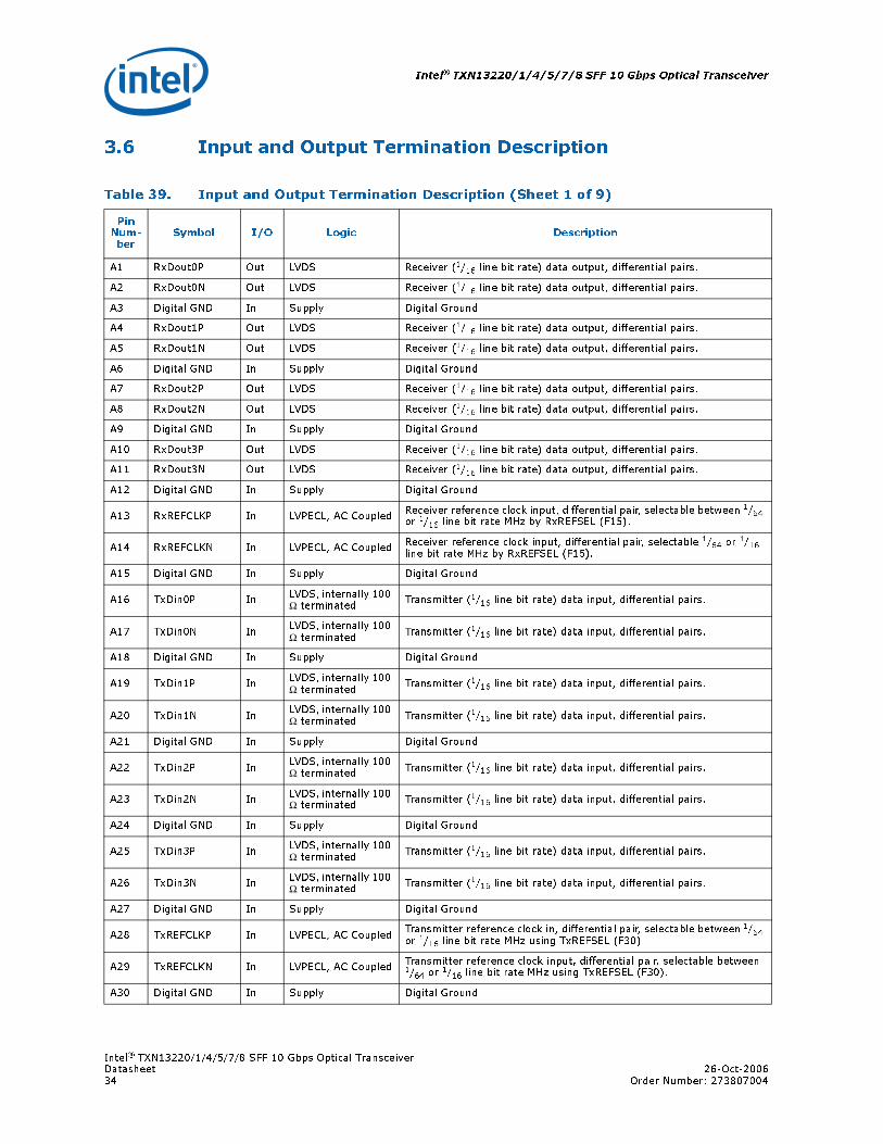
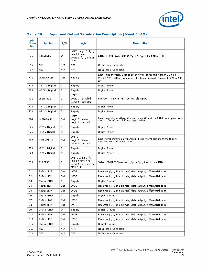
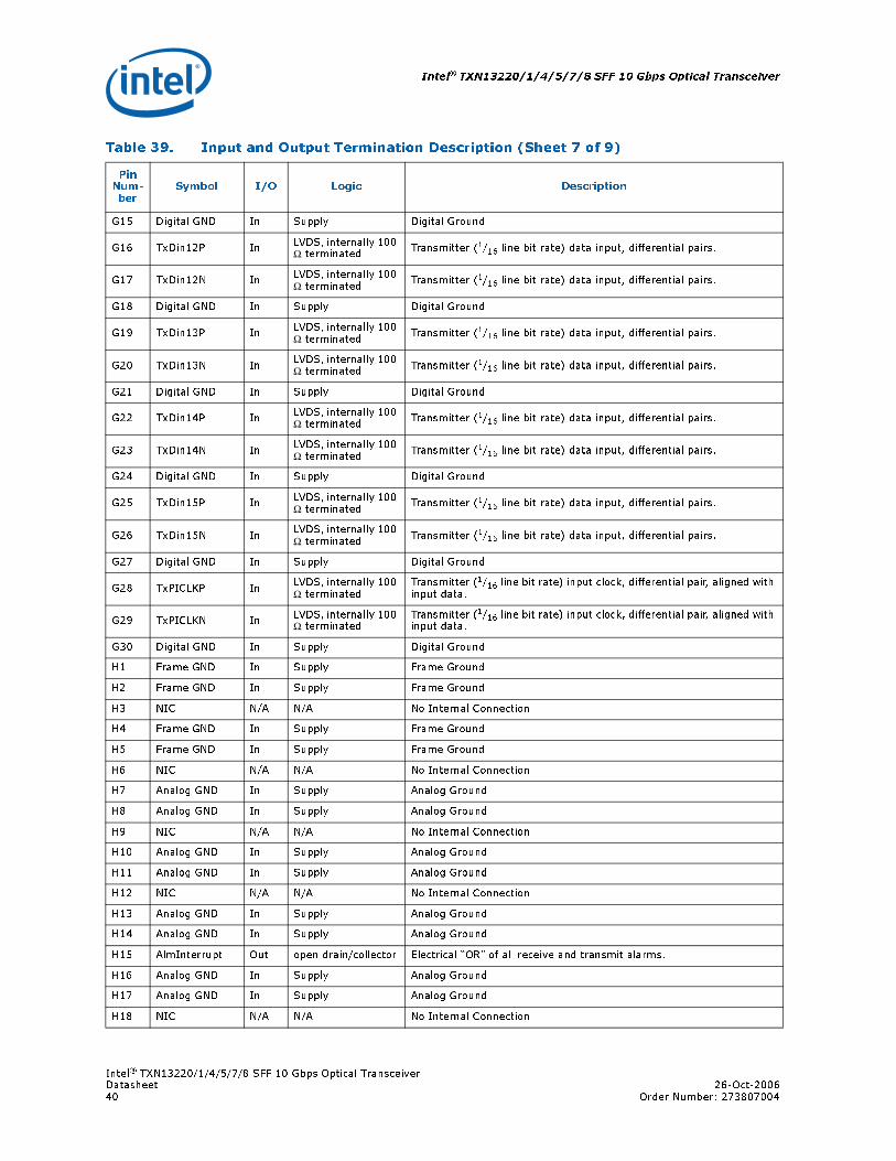
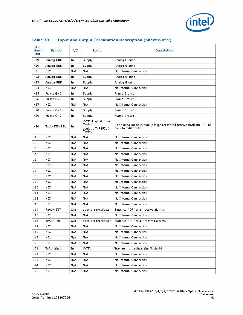
3.6 Input and Output Termination Description
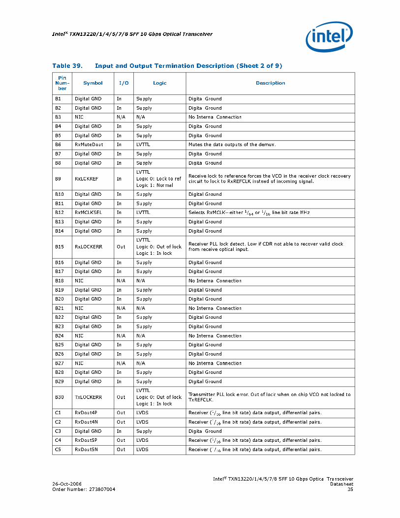
Table 39. Input and Output Termination Description (Sheet 1 of 9)
Pin Num-ber
Symbol I/O Logic Description
A1 RxDout0P Out LVDS Receiver (1/16 line bit rate) data output, differential pairs.
A2 RxDout0N Out LVDS Receiver (1/16 line bit rate) data output, differential pairs.
A3 Digital GND In Supply Digital Ground
A4 RxDout1P Out LVDS Receiver (1/16 line bit rate) data output, differential pairs.
A5 RxDout1N Out LVDS Receiver (1/16 line bit rate) data output, differential pairs.
A6 Digital GND In Supply Digital Ground
A7 RxDout2P Out LVDS Receiver (1/16 line bit rate) data output, differential pairs.
A8 RxDout2N Out LVDS Receiver (1/16 line bit rate) data output, differential pairs.
A9 Digital GND In Supply Digital Ground
A10 RxDout3P Out LVDS Receiver (1/16 line bit rate) data output, differential pairs.
A11 RxDout3N Out LVDS Receiver (1/16 line bit rate) data output, differential pairs.
A12 Digital GND In Supply Digital Ground
A13 RxREFCLKP In LVPECL, AC CoupledReceiver reference clock input, differential pair, selectable between 1/64 or 1/16 line bit rate MHz by RxREFSEL (F15).
A14 RxREFCLKN In LVPECL, AC CoupledReceiver reference clock input, differential pair, selectable 1/64 or 1/16 line bit rate MHz by RxREFSEL (F15).
A15 Digital GND In Supply Digital Ground
A16 TxDin0P InLVDS, internally 100 Ω terminated
Transmitter (1/16 line bit rate) data input, differential pairs.
A17 TxDin0N InLVDS, internally 100 Ω terminated
Transmitter (1/16 line bit rate) data input, differential pairs.
A18 Digital GND In Supply Digital Ground
A19 TxDin1P InLVDS, internally 100 Ω terminated
Transmitter (1/16 line bit rate) data input, differential pairs.
A20 TxDin1N InLVDS, internally 100 Ω terminated
Transmitter (1/16 line bit rate) data input, differential pairs.
A21 Digital GND In Supply Digital Ground
A22 TxDin2P InLVDS, internally 100 Ω terminated
Transmitter (1/16 line bit rate) data input, differential pairs.
A23 TxDin2N InLVDS, internally 100 Ω terminated
Transmitter (1/16 line bit rate) data input, differential pairs.
A24 Digital GND In Supply Digital Ground
A25 TxDin3P InLVDS, internally 100 Ω terminated
Transmitter (1/16 line bit rate) data input, differential pairs.
A26 TxDin3N InLVDS, internally 100 Ω terminated
Transmitter (1/16 line bit rate) data input, differential pairs.
A27 Digital GND In Supply Digital Ground
A28 TxREFCLKP In LVPECL, AC CoupledTransmitter reference clock in, differential pair, selectable between 1/64 or 1/16 line bit rate MHz using TxREFSEL (F30).
A29 TxREFCLKN In LVPECL, AC CoupledTransmitter reference clock input, differential pair, selectable between
1/64 or 1/16 line bit rate MHz using TxREFSEL (F30).
A30 Digital GND In Supply Digital Ground
Intel® TXN13220/1/4/5/7/8 SFF 10 Gbps Optical Transceiver26-Oct-2006 DatasheetOrder Number: 273807004 35
Intel® TXN13220/1/4/5/7/8 SFF 10 Gbps Optical Transceiver
B1 Digital GND In Supply Digital Ground
B2 Digital GND In Supply Digital Ground
B3 NIC N/A N/A No Internal Connection
B4 Digital GND In Supply Digital Ground
B5 Digital GND In Supply Digital Ground
B6 RxMuteDout In LVTTL Mutes the data outputs of the demux.
B7 Digital GND In Supply Digital Ground
B8 Digital GND In Supply Digital Ground
B9 RxLCKREF In
LVTTL
Logic 0: Lock to ref
Logic 1: Normal
Receive lock to reference forces the VCO in the receiver clock recovery circuit to lock to RxREFCLK instead of incoming signal.
B10 Digital GND In Supply Digital Ground
B11 Digital GND In Supply Digital Ground
B12 RxMCLKSEL In LVTTL Selects RxMCLK—either 1/64 or 1/16 line bit rate MHz.
B13 Digital GND In Supply Digital Ground
B14 Digital GND In Supply Digital Ground
B15 RxLOCKERR Out
LVTTL
Logic 0: Out of lock
Logic 1: In lock
Receiver PLL lock detect. Low if CDR not able to recover valid clock from receive optical input.
B16 Digital GND In Supply Digital Ground
B17 Digital GND In Supply Digital Ground
B18 NIC N/A N/A No Internal Connection
B19 Digital GND In Supply Digital Ground
B20 Digital GND In Supply Digital Ground
B21 NIC N/A N/A No Internal Connection
B22 Digital GND In Supply Digital Ground
B23 Digital GND In Supply Digital Ground
B24 NIC N/A N/A No Internal Connection
B25 Digital GND In Supply Digital Ground
B26 Digital GND In Supply Digital Ground
B27 NIC N/A N/A No Internal Connection
B28 Digital GND In Supply Digital Ground
B29 Digital GND In Supply Digital Ground
B30 TxLOCKERR Out
LVTTL
Logic 0: Out of lock
Logic 1: In lock
Transmitter PLL lock error. Out of lock when on chip VCO not locked to TxREFCLK.
C1 RxDout4P Out LVDS Receiver (1/16 line bit rate) data output, differential pairs.
C2 RxDout4N Out LVDS Receiver (1/16 line bit rate) data output, differential pairs.
C3 Digital GND In Supply Digital Ground
C4 RxDout5P Out LVDS Receiver (1/16 line bit rate) data output, differential pairs.
C5 RxDout5N Out LVDS Receiver (1/16 line bit rate) data output, differential pairs.
Table 39. Input and Output Termination Description (Sheet 2 of 9)
Pin Num-ber
Symbol I/O Logic Description
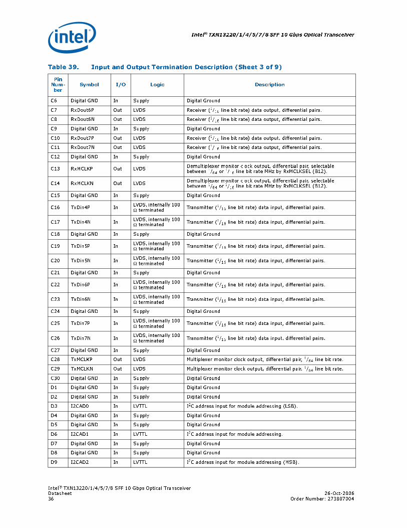
Intel® TXN13220/1/4/5/7/8 SFF 10 Gbps Optical Transceiver
Intel® TXN13220/1/4/5/7/8 SFF 10 Gbps Optical TransceiverDatasheet 26-Oct-200636 Order Number: 273807004
C6 Digital GND In Supply Digital Ground
C7 RxDout6P Out LVDS Receiver (1/16 line bit rate) data output, differential pairs.
C8 RxDout6N Out LVDS Receiver (1/16 line bit rate) data output, differential pairs.
C9 Digital GND In Supply Digital Ground
C10 RxDout7P Out LVDS Receiver (1/16 line bit rate) data output, differential pairs.
C11 RxDout7N Out LVDS Receiver (1/16 line bit rate) data output, differential pairs.
C12 Digital GND In Supply Digital Ground
C13 RxMCLKP Out LVDSDemultiplexer monitor clock output, differential pair, selectable between 1/64 or 1/16 line bit rate MHz by RxMCLKSEL (B12).
C14 RxMCLKN Out LVDSDemultiplexer monitor clock output, differential pair, selectable between 1/64 or 1/16 line bit rate MHz by RxMCLKSEL (B12).
C15 Digital GND In Supply Digital Ground
C16 TxDin4P InLVDS, internally 100 Ω terminated
Transmitter (1/16 line bit rate) data input, differential pairs.
C17 TxDin4N InLVDS, internally 100 Ω terminated
Transmitter (1/16 line bit rate) data input, differential pairs.
C18 Digital GND In Supply Digital Ground
C19 TxDin5P InLVDS, internally 100 Ω terminated
Transmitter (1/16 line bit rate) data input, differential pairs.
C20 TxDin5N InLVDS, internally 100 Ω terminated
Transmitter (1/16 line bit rate) data input, differential pairs.
C21 Digital GND In Supply Digital Ground
C22 TxDin6P InLVDS, internally 100 Ω terminated
Transmitter (1/16 line bit rate) data input, differential pairs.
C23 TxDin6N InLVDS, internally 100 Ω terminated
Transmitter (1/16 line bit rate) data input, differential pairs.
C24 Digital GND In Supply Digital Ground
C25 TxDin7P InLVDS, internally 100 Ω terminated
Transmitter (1/16 line bit rate) data input, differential pairs.
C26 TxDin7N InLVDS, internally 100 Ω terminated
Transmitter (1/16 line bit rate) data input, differential pairs.
C27 Digital GND In Supply Digital Ground
C28 TxMCLKP Out LVDS Multiplexer monitor clock output, differential pair, 1/64 line bit rate.
C29 TxMCLKN Out LVDS Multiplexer monitor clock output, differential pair, 1/64 line bit rate.
C30 Digital GND In Supply Digital Ground
D1 Digital GND In Supply Digital Ground
D2 Digital GND In Supply Digital Ground
D3 I2CAD0 In LVTTL I2C address input for module addressing (LSB).
D4 Digital GND In Supply Digital Ground
D5 Digital GND In Supply Digital Ground
D6 I2CAD1 In LVTTL I2C address input for module addressing.
D7 Digital GND In Supply Digital Ground
D8 Digital GND In Supply Digital Ground
D9 I2CAD2 In LVTTL I2C address input for module addressing (MSB).
Table 39. Input and Output Termination Description (Sheet 3 of 9)
Pin Num-ber
Symbol I/O Logic Description
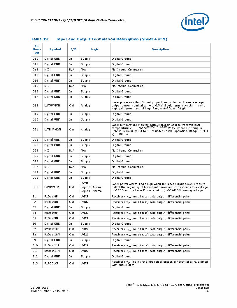
Intel® TXN13220/1/4/5/7/8 SFF 10 Gbps Optical Transceiver26-Oct-2006 DatasheetOrder Number: 273807004 37
Intel® TXN13220/1/4/5/7/8 SFF 10 Gbps Optical Transceiver
D10 Digital GND In Supply Digital Ground
D11 Digital GND In Supply Digital Ground
D12 NIC N/A N/A No Internal Connection
D13 Digital GND In Supply Digital Ground
D14 Digital GND In Supply Digital Ground
D15 NIC N/A N/A No Internal Connection
D16 Digital GND In Supply Digital Ground
D17 Digital GND In Supply Digital Ground
D18 LsPOWMON Out AnalogLaser power monitor. Output proportional to transmit laser average output power. Nominal value of 0.5 V should remain constant due to high gain power control loop. Range: 0–2 V, ± 100 µA
D19 Digital GND In Supply Digital Ground
D20 Digital GND In Supply Digital Ground
D21 LsTEMPMON Out Analog
Laser temperature monitor. Output proportional to transmit laser temperature V = 0.764*e3887*(1/T - 1/298) Volts, where T is temp in Kelvins. Nominally 0.4 to 0.6 V under normal operation. Range: 0–3.3 V, ± 100 µA
D22 Digital GND In Supply Digital Ground
D23 Digital GND In Supply Digital Ground
D24 NIC N/A N/A No Internal Connection
D25 Digital GND In Supply Digital Ground
D26 Digital GND In Supply Digital Ground
D27 NIC N/A N/A No Internal Connection
D28 Digital GND In Supply Digital Ground
D29 Digital GND In Supply Digital Ground
D30 LsPOWALM Out
LVTTL
Logic 0: Alarm
Logic 1: Normal
Laser power alarm. Logic high when the laser output power drops to half of the beginning of life output power, and corresponds to a voltage of 0.25 V on the Laser Power Monitor (LsPOWMON) analog voltage.
E1 RxDout8P Out LVDS Receiver (1/16 line bit rate) data output, differential pairs.
E2 RxDout8N Out LVDS Receiver (1/16 line bit rate) data output, differential pairs.
E3 Digital GND In Supply Digital Ground
E4 RxDout9P Out LVDS Receiver (1/16 line bit rate) data output, differential pairs.
E5 RxDout9N Out LVDS Receiver (1/16 line bit rate) data output, differential pairs.
E6 Digital GND In Supply Digital Ground
E7 RxDout10P Out LVDS Receiver (1/16 line bit rate) data output, differential pairs.
E8 RxDout10N Out LVDS Receiver (1/16 line bit rate) data output, differential pairs.
E9 Digital GND In Supply Digital Ground
E10 RxDout11P Out LVDS Receiver (1/16 line bit rate) data output, differential pairs.
E11 RxDout11N Out LVDS Receiver (1/16 line bit rate) data output, differential pairs.
E12 Digital GND In Supply Digital Ground
E13 RxPOCLKP Out LVDSReceiver (1/16 line bit rate MHz) clock output, differential pairs, aligned with output data.
Table 39. Input and Output Termination Description (Sheet 4 of 9)
Pin Num-ber
Symbol I/O Logic Description
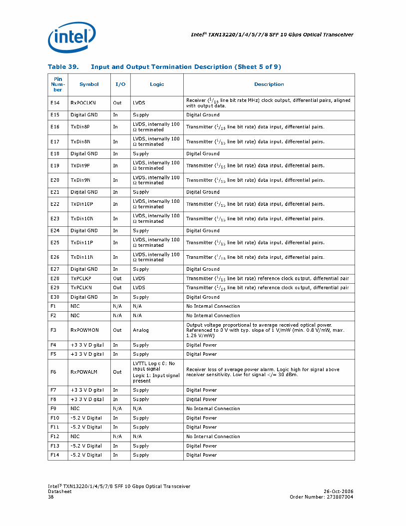
Intel® TXN13220/1/4/5/7/8 SFF 10 Gbps Optical Transceiver
Intel® TXN13220/1/4/5/7/8 SFF 10 Gbps Optical TransceiverDatasheet 26-Oct-200638 Order Number: 273807004
E14 RxPOCLKN Out LVDSReceiver (1/16 line bit rate MHz) clock output, differential pairs, aligned with output data.
E15 Digital GND In Supply Digital Ground
E16 TxDin8P InLVDS, internally 100 Ω terminated
Transmitter (1/16 line bit rate) data input, differential pairs.
E17 TxDin8N InLVDS, internally 100 Ω terminated
Transmitter (1/16 line bit rate) data input, differential pairs.
E18 Digital GND In Supply Digital Ground
E19 TxDin9P InLVDS, internally 100 Ω terminated
Transmitter (1/16 line bit rate) data input, differential pairs.
E20 TxDin9N InLVDS, internally 100 Ω terminated
Transmitter (1/16 line bit rate) data input, differential pairs.
E21 Digital GND In Supply Digital Ground
E22 TxDin10P InLVDS, internally 100 Ω terminated
Transmitter (1/16 line bit rate) data input, differential pairs.
E23 TxDin10N InLVDS, internally 100 Ω terminated
Transmitter (1/16 line bit rate) data input, differential pairs.
E24 Digital GND In Supply Digital Ground
E25 TxDin11P InLVDS, internally 100 Ω terminated
Transmitter (1/16 line bit rate) data input, differential pairs.
E26 TxDin11N InLVDS, internally 100 Ω terminated
Transmitter (1/16 line bit rate) data input, differential pairs.
E27 Digital GND In Supply Digital Ground
E28 TxPCLKP Out LVDS Transmitter (1/16 line bit rate) reference clock output, differential pair
E29 TxPCLKN Out LVDS Transmitter (1/16 line bit rate) reference clock output, differential pair
E30 Digital GND In Supply Digital Ground
F1 NIC N/A N/A No Internal Connection
F2 NIC N/A N/A No Internal Connection
F3 RxPOWMON Out AnalogOutput voltage proportional to average received optical power. Referenced to 0 V with typ. slope of 1 V/mW (min. 0.8 V/mW, max. 1.26 V/mW)
F4 +3.3 V Digital In Supply Digital Power
F5 +3.3 V Digital In Supply Digital Power
F6 RxPOWALM Out
LVTTL Logic 0: No input signal
Logic 1: Input signal present
Receiver loss of average power alarm. Logic high for signal above receiver sensitivity. Low for signal </= 30 dBm.
F7 +3.3 V Digital In Supply Digital Power
F8 +3.3 V Digital In Supply Digital Power
F9 NIC N/A N/A No Internal Connection
F10 -5.2 V Digital In Supply Digital Power
F11 -5.2 V Digital In Supply Digital Power
F12 NIC N/A N/A No Internal Connection
F13 -5.2 V Digital In Supply Digital Power
F14 -5.2 V Digital In Supply Digital Power
Table 39. Input and Output Termination Description (Sheet 5 of 9)
Pin Num-ber
Symbol I/O Logic Description
Intel® TXN13220/1/4/5/7/8 SFF 10 Gbps Optical Transceiver26-Oct-2006 DatasheetOrder Number: 273807004 39
Intel® TXN13220/1/4/5/7/8 SFF 10 Gbps Optical Transceiver
F15 RxREFSEL In
LVTTL Logic 0: 1/64 line bit rate
Logic 1: 1/16 line bit rate
Selects RxREFCLK—either 1/64 or 1/16 line bit rate MHz.
F16 NIC N/A N/A No Internal Connection
F17 NIC N/A N/A No Internal Connection
F18 LsBIASMON Out AnalogLaser bias monitor. Output proportional to transmit laser DC bias
V = 20 * (1 - Offset) mV where I = laser bias mA. Range: 0–2 V, ± 100 µA
F19 +3.3 V Digital In Supply Digital Power
F20 +3.3 V Digital In Supply Digital Power
F21 LsENABLE In
LVTTL
Logic 0: Enabled
Logic 1: Disabled
Function: Transmitter laser enable input.
F22 +3.3 V Digital In Supply Digital Power
F23 +3.3 V Digital In Supply Digital Power
F24 LsBIASALM OutLVTTL Logic 0: AlarmLogic 1: Normal
Laser bias alarm. Alarm if laser bias > 80 mA for 1310 nm applications and > 100 mA for 1550 nm applications.
F25 -5.2 V Digital In Supply Digital Power
F26 -5.2 V Digital In Supply Digital Power
F27 LsTEMPALM Out
LVTTL
Logic 0: Alarm
Logic 1: Normal
Laser temperature alarm. Alarm if laser temperature more than 5 degrees from initial set point.
F28 -5.2 V Digital In Supply Digital Power
F29 -5.2 V Digital In Supply Digital Power
F30 TxREFSEL In
LVTTL Logic 0: 1/64 line bit rate MHz
Logic 1: 1/16 line bit rate MHz
Selects TxREFSEL—either 1/64 or 1/16 line bit rate MHz.
G1 RxDout12P Out LVDS Receiver (1/16 line bit rate) data output, differential pairs.
G2 RxDout12N Out LVDS Receiver (1/16 line bit rate) data output, differential pairs.
G3 Digital GND In Supply Digital Ground
G4 RxDout13P Out LVDS Receiver (1/16 line bit rate) data output, differential pairs.
G5 RxDout13N Out LVDS Receiver (1/16 line bit rate) data output, differential pairs.
G6 Digital GND In Supply Digital Ground
G7 RxDout14P Out LVDS Receiver (1/16 line bit rate) data output, differential pairs.
G8 RxDout14N Out LVDS Receiver (1/16 line bit rate) data output, differential pairs.
G9 Digital GND In Supply Digital Ground
G10 RxDout15P Out LVDS Receiver (1/16 line bit rate) data output, differential pairs.
G11 RxDout15N Out LVDS Receiver (1/16 line bit rate) data output, differential pairs.
G12 Digital GND In Supply Digital Ground
G13 NIC N/A N/A No Internal Connection
G14 NIC N/A N/A No Internal Connection
Table 39. Input and Output Termination Description (Sheet 6 of 9)
Pin Num-ber
Symbol I/O Logic Description
Intel® TXN13220/1/4/5/7/8 SFF 10 Gbps Optical Transceiver
Intel® TXN13220/1/4/5/7/8 SFF 10 Gbps Optical TransceiverDatasheet 26-Oct-200640 Order Number: 273807004
G15 Digital GND In Supply Digital Ground
G16 TxDin12P InLVDS, internally 100 Ω terminated
Transmitter (1/16 line bit rate) data input, differential pairs.
G17 TxDin12N InLVDS, internally 100 Ω terminated
Transmitter (1/16 line bit rate) data input, differential pairs.
G18 Digital GND In Supply Digital Ground
G19 TxDin13P InLVDS, internally 100 Ω terminated
Transmitter (1/16 line bit rate) data input, differential pairs.
G20 TxDin13N InLVDS, internally 100 Ω terminated
Transmitter (1/16 line bit rate) data input, differential pairs.
G21 Digital GND In Supply Digital Ground
G22 TxDin14P InLVDS, internally 100 Ω terminated
Transmitter (1/16 line bit rate) data input, differential pairs.
G23 TxDin14N InLVDS, internally 100 Ω terminated
Transmitter (1/16 line bit rate) data input, differential pairs.
G24 Digital GND In Supply Digital Ground
G25 TxDin15P InLVDS, internally 100 Ω terminated
Transmitter (1/16 line bit rate) data input, differential pairs.
G26 TxDin15N InLVDS, internally 100 Ω terminated
Transmitter (1/16 line bit rate) data input, differential pairs.
G27 Digital GND In Supply Digital Ground
G28 TxPICLKP InLVDS, internally 100 Ω terminated
Transmitter (1/16 line bit rate) input clock, differential pair, aligned with input data.
G29 TxPICLKN InLVDS, internally 100 Ω terminated
Transmitter (1/16 line bit rate) input clock, differential pair, aligned with input data.
G30 Digital GND In Supply Digital Ground
H1 Frame GND In Supply Frame Ground
H2 Frame GND In Supply Frame Ground
H3 NIC N/A N/A No Internal Connection
H4 Frame GND In Supply Frame Ground
H5 Frame GND In Supply Frame Ground
H6 NIC N/A N/A No Internal Connection
H7 Analog GND In Supply Analog Ground
H8 Analog GND In Supply Analog Ground
H9 NIC N/A N/A No Internal Connection
H10 Analog GND In Supply Analog Ground
H11 Analog GND In Supply Analog Ground
H12 NIC N/A N/A No Internal Connection
H13 Analog GND In Supply Analog Ground
H14 Analog GND In Supply Analog Ground
H15 AlmInterrupt Out open drain/collector Electrical “OR” of all receive and transmit alarms.
H16 Analog GND In Supply Analog Ground
H17 Analog GND In Supply Analog Ground
H18 NIC N/A N/A No Internal Connection
Table 39. Input and Output Termination Description (Sheet 7 of 9)
Pin Num-ber
Symbol I/O Logic Description
Intel® TXN13220/1/4/5/7/8 SFF 10 Gbps Optical Transceiver26-Oct-2006 DatasheetOrder Number: 273807004 41
Intel® TXN13220/1/4/5/7/8 SFF 10 Gbps Optical Transceiver
H19 Analog GND In Supply Analog Ground
H20 Analog GND In Supply Analog Ground
H21 NIC N/A N/A No Internal Connection
H22 Analog GND In Supply Analog Ground
H23 Analog GND In Supply Analog Ground
H24 NIC N/A N/A No Internal Connection
H25 Frame GND In Supply Frame Ground
H26 Frame GND In Supply Frame Ground
H27 NIC N/A N/A No Internal Connection
H28 Frame GND In Supply Frame Ground
H29 Frame GND In Supply Frame Ground
H30 TxLINETIMSEL In
LVTTL Logic 0: Line Timing
Logic 1: TxREFCLK Timing
Line timing mode internally loops recovered receive clock (RxPOCLK) back to TxREFCLK.
J1 NIC N/A N/A No Internal Connection
J2 NIC N/A N/A No Internal Connection
J3 NIC N/A N/A No Internal Connection
J4 NIC N/A N/A No Internal Connection
J5 NIC N/A N/A No Internal Connection
J6 NIC N/A N/A No Internal Connection
J7 NIC N/A N/A No Internal Connection
J8 NIC N/A N/A No Internal Connection
J9 NIC N/A N/A No Internal Connection
J10 NIC N/A N/A No Internal Connection
J11 NIC N/A N/A No Internal Connection
J12 NIC N/A N/A No Internal Connection
J13 NIC N/A N/A No Internal Connection
J14 RxALM INT Out open drain/collector Electrical “OR” of all receive alarms.
J15 NIC N/A N/A No Internal Connection
J16 TxALM INT Out open drain/collector Electrical “OR” of all transmit alarms.
J17 NIC N/A N/A No Internal Connection
J18 NIC N/A N/A No Internal Connection
J19 NIC N/A N/A No Internal Connection
J20 NIC N/A N/A No Internal Connection
J21 TxRateSel1 In LVTTL Transmit rate select. See Table 34.
J22 NIC N/A N/A No Internal Connection
J23 NIC N/A N/A No Internal Connection
J24 NIC N/A N/A No Internal Connection
J25 NIC N/A N/A No Internal Connection
Table 39. Input and Output Termination Description (Sheet 8 of 9)
Pin Num-ber
Symbol I/O Logic Description
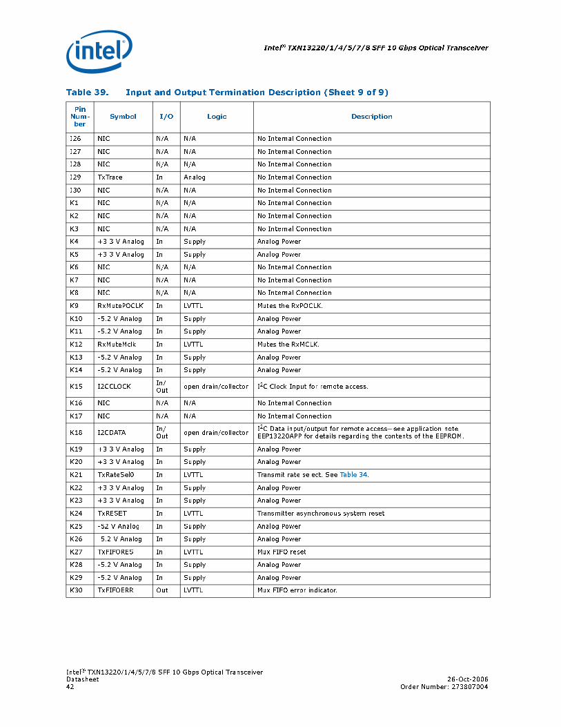
Intel® TXN13220/1/4/5/7/8 SFF 10 Gbps Optical Transceiver
Intel® TXN13220/1/4/5/7/8 SFF 10 Gbps Optical TransceiverDatasheet 26-Oct-200642 Order Number: 273807004
J26 NIC N/A N/A No Internal Connection
J27 NIC N/A N/A No Internal Connection
J28 NIC N/A N/A No Internal Connection
J29 TxTrace In Analog No Internal Connection
J30 NIC N/A N/A No Internal Connection
K1 NIC N/A N/A No Internal Connection
K2 NIC N/A N/A No Internal Connection
K3 NIC N/A N/A No Internal Connection
K4 +3.3 V Analog In Supply Analog Power
K5 +3.3 V Analog In Supply Analog Power
K6 NIC N/A N/A No Internal Connection
K7 NIC N/A N/A No Internal Connection
K8 NIC N/A N/A No Internal Connection
K9 RxMutePOCLK In LVTTL Mutes the RxPOCLK.
K10 -5.2 V Analog In Supply Analog Power
K11 -5.2 V Analog In Supply Analog Power
K12 RxMuteMclk In LVTTL Mutes the RxMCLK.
K13 -5.2 V Analog In Supply Analog Power
K14 -5.2 V Analog In Supply Analog Power
K15 I2CCLOCKIn/Out
open drain/collector I2C Clock Input for remote access.
K16 NIC N/A N/A No Internal Connection
K17 NIC N/A N/A No Internal Connection
K18 I2CDATAIn/Out
open drain/collectorI2C Data input/output for remote access—see application note EEP13220APP for details regarding the contents of the EEPROM.
K19 +3.3 V Analog In Supply Analog Power
K20 +3.3 V Analog In Supply Analog Power
K21 TxRateSel0 In LVTTL Transmit rate select. See Table 34.
K22 +3.3 V Analog In Supply Analog Power
K23 +3.3 V Analog In Supply Analog Power
K24 TxRESET In LVTTL Transmitter asynchronous system reset
K25 -52 V Analog In Supply Analog Power
K26 -5.2 V Analog In Supply Analog Power
K27 TxFIFORES In LVTTL Mux FIFO reset
K28 -5.2 V Analog In Supply Analog Power
K29 -5.2 V Analog In Supply Analog Power
K30 TxFIFOERR Out LVTTL Mux FIFO error indicator.
Table 39. Input and Output Termination Description (Sheet 9 of 9)
Pin Num-ber
Symbol I/O Logic Description
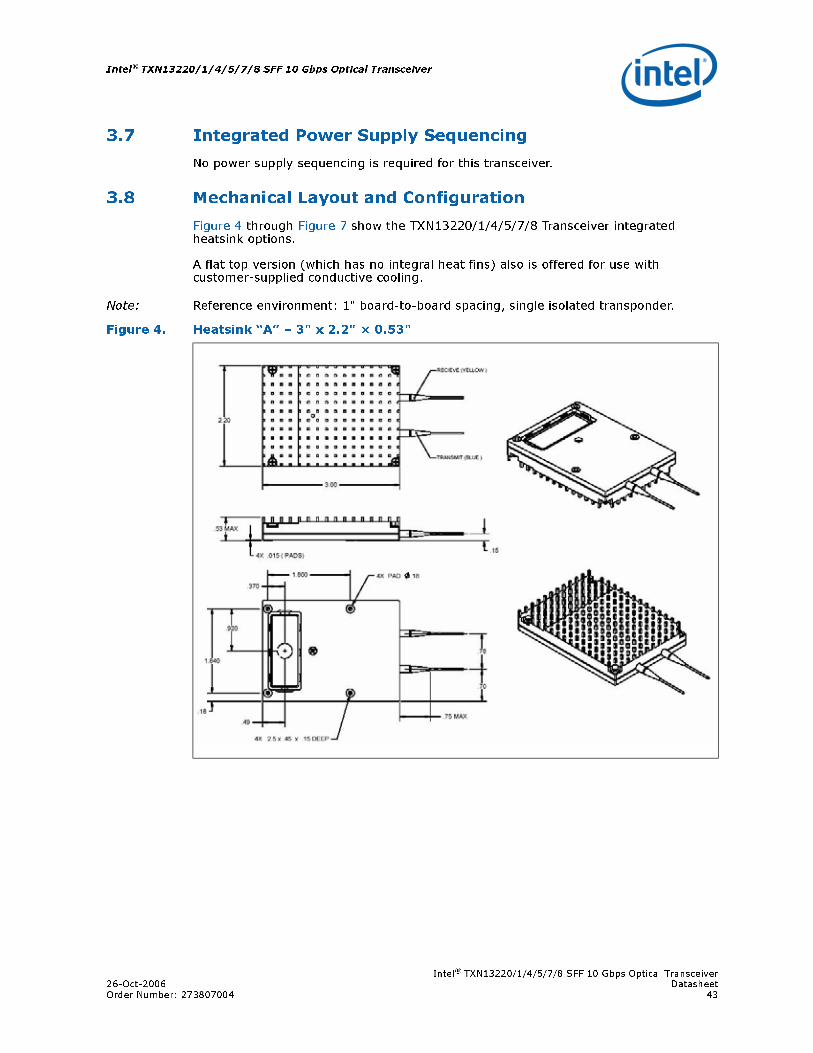
Intel® TXN13220/1/4/5/7/8 SFF 10 Gbps Optical Transceiver26-Oct-2006 DatasheetOrder Number: 273807004 43
Intel® TXN13220/1/4/5/7/8 SFF 10 Gbps Optical Transceiver
3.7 Integrated Power Supply Sequencing
No power supply sequencing is required for this transceiver.
3.8 Mechanical Layout and Configuration
Figure 4 through Figure 7 show the TXN13220/1/4/5/7/8 Transceiver integrated heatsink options.
A flat top version (which has no integral heat fins) also is offered for use with customer-supplied conductive cooling.
Note: Reference environment: 1" board-to-board spacing, single isolated transponder.
Figure 4. Heatsink “A” – 3" x 2.2" × 0.53"
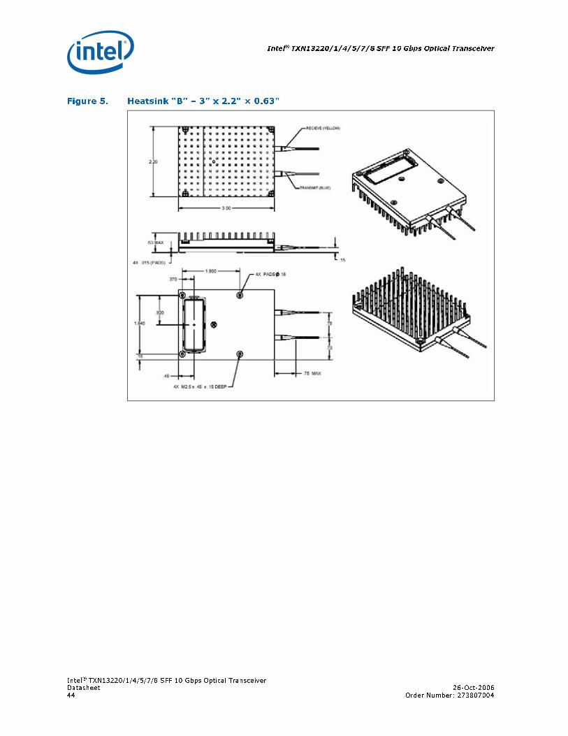
Intel® TXN13220/1/4/5/7/8 SFF 10 Gbps Optical Transceiver
Intel® TXN13220/1/4/5/7/8 SFF 10 Gbps Optical TransceiverDatasheet 26-Oct-200644 Order Number: 273807004
Figure 5. Heatsink “B” – 3" x 2.2" × 0.63"
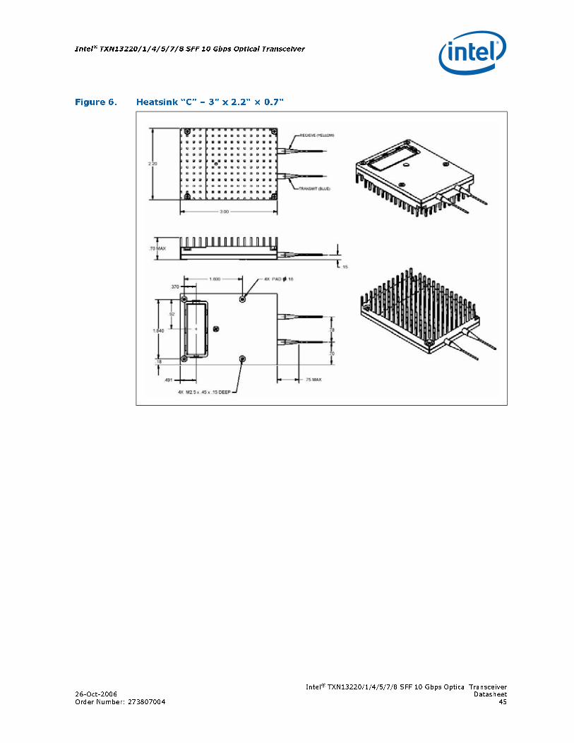
Intel® TXN13220/1/4/5/7/8 SFF 10 Gbps Optical Transceiver26-Oct-2006 DatasheetOrder Number: 273807004 45
Intel® TXN13220/1/4/5/7/8 SFF 10 Gbps Optical Transceiver
Figure 6. Heatsink “C” – 3" x 2.2" × 0.7"
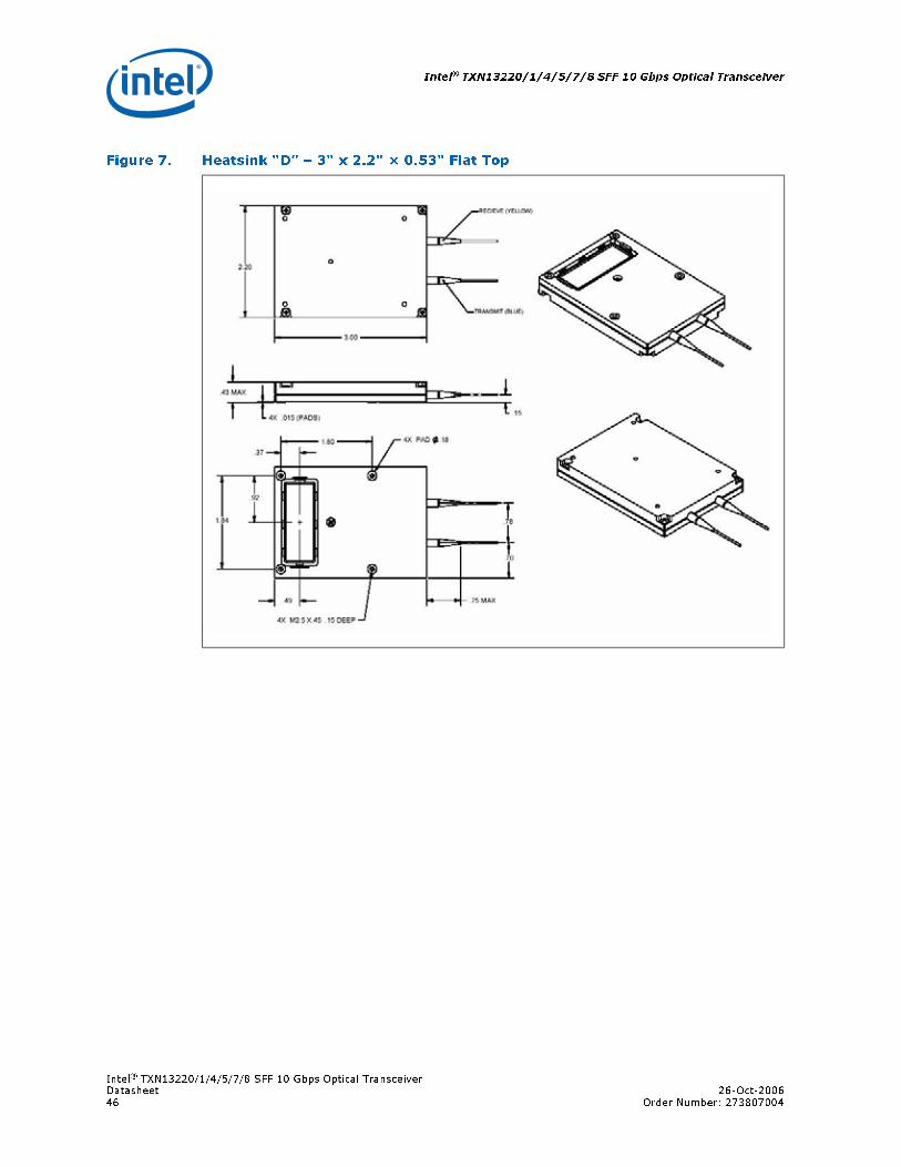
Intel® TXN13220/1/4/5/7/8 SFF 10 Gbps Optical Transceiver
Intel® TXN13220/1/4/5/7/8 SFF 10 Gbps Optical TransceiverDatasheet 26-Oct-200646 Order Number: 273807004
Figure 7. Heatsink “D” – 3" x 2.2" × 0.53" Flat Top
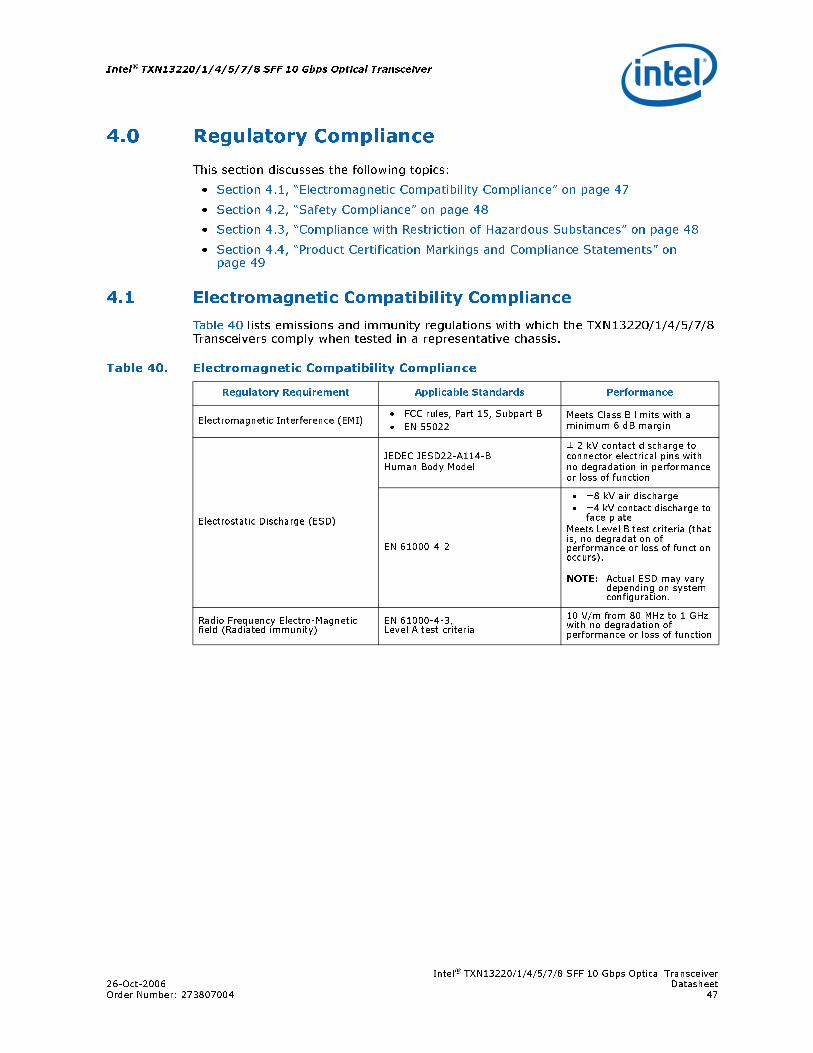
Intel® TXN13220/1/4/5/7/8 SFF 10 Gbps Optical Transceiver26-Oct-2006 DatasheetOrder Number: 273807004 47
Intel® TXN13220/1/4/5/7/8 SFF 10 Gbps Optical Transceiver
4.0 Regulatory Compliance
This section discusses the following topics:
• Section 4.1, “Electromagnetic Compatibility Compliance” on page 47
• Section 4.2, “Safety Compliance” on page 48
• Section 4.3, “Compliance with Restriction of Hazardous Substances” on page 48
• Section 4.4, “Product Certification Markings and Compliance Statements” on page 49
4.1 Electromagnetic Compatibility Compliance
Table 40 lists emissions and immunity regulations with which the TXN13220/1/4/5/7/8 Transceivers comply when tested in a representative chassis.
Table 40. Electromagnetic Compatibility Compliance
Regulatory Requirement Applicable Standards Performance
Electromagnetic Interference (EMI)• FCC rules, Part 15, Subpart B
• EN 55022Meets Class B limits with a minimum 6 dB margin
Electrostatic Discharge (ESD)
JEDEC JESD22-A114-B Human Body Model
± 2 kV contact discharge to connector electrical pins with no degradation in performance or loss of function
EN 61000-4-2
• ±8 kV air discharge• ±4 kV contact discharge to
face plate Meets Level B test criteria (that is, no degradation of performance or loss of function occurs).
NOTE: Actual ESD may vary depending on system configuration.
Radio Frequency Electro-Magnetic field (Radiated immunity)
EN 61000-4-3, Level A test criteria
10 V/m from 80 MHz to 1 GHz with no degradation of performance or loss of function
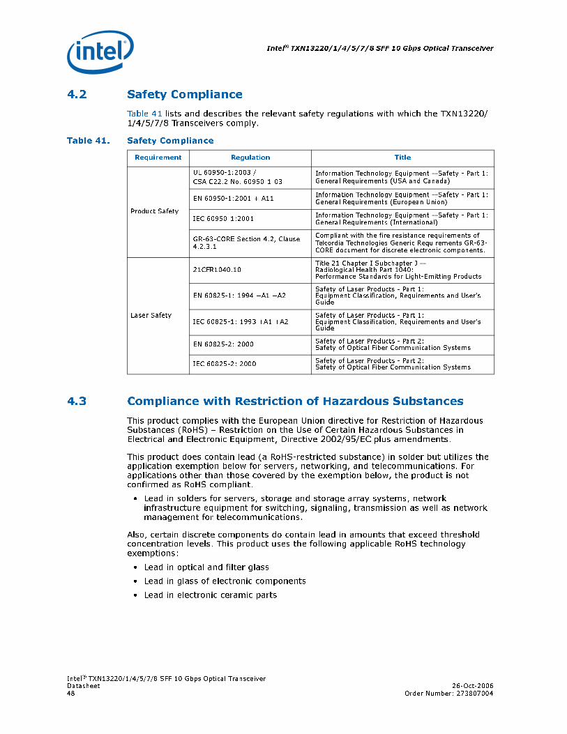
Intel® TXN13220/1/4/5/7/8 SFF 10 Gbps Optical Transceiver
Intel® TXN13220/1/4/5/7/8 SFF 10 Gbps Optical TransceiverDatasheet 26-Oct-200648 Order Number: 273807004
4.2 Safety Compliance
Table 41 lists and describes the relevant safety regulations with which the TXN13220/1/4/5/7/8 Transceivers comply.
4.3 Compliance with Restriction of Hazardous Substances
This product complies with the European Union directive for Restriction of Hazardous Substances (RoHS) – Restriction on the Use of Certain Hazardous Substances in Electrical and Electronic Equipment, Directive 2002/95/EC plus amendments.
This product does contain lead (a RoHS-restricted substance) in solder but utilizes the application exemption below for servers, networking, and telecommunications. For applications other than those covered by the exemption below, the product is not confirmed as RoHS compliant.
• Lead in solders for servers, storage and storage array systems, network infrastructure equipment for switching, signaling, transmission as well as network management for telecommunications.
Also, certain discrete components do contain lead in amounts that exceed threshold concentration levels. This product uses the following applicable RoHS technology exemptions:
• Lead in optical and filter glass
• Lead in glass of electronic components
• Lead in electronic ceramic parts
Table 41. Safety Compliance
Requirement Regulation Title
Product Safety
UL 60950-1:2003 /
CSA C22.2 No. 60950-1-03Information Technology Equipment – Safety - Part 1:General Requirements (USA and Canada)
EN 60950-1:2001 + A11Information Technology Equipment – Safety - Part 1:General Requirements (European Union)
IEC 60950-1:2001Information Technology Equipment – Safety - Part 1:General Requirements (International)
GR-63-CORE Section 4.2, Clause 4.2.3.1
Compliant with the fire resistance requirements of Telcordia Technologies Generic Requirements GR-63-CORE document for discrete electronic components.
Laser Safety
21CFR1040.10Title 21 Chapter I Subchapter J – Radiological Health Part 1040: Performance Standards for Light-Emitting Products
EN 60825-1: 1994 +A1 +A2Safety of Laser Products - Part 1: Equipment Classification, Requirements and User's Guide
IEC 60825-1: 1993 +A1 +A2Safety of Laser Products - Part 1: Equipment Classification, Requirements and User's Guide
EN 60825-2: 2000 Safety of Laser Products - Part 2: Safety of Optical Fiber Communication Systems
IEC 60825-2: 2000 Safety of Laser Products - Part 2: Safety of Optical Fiber Communication Systems
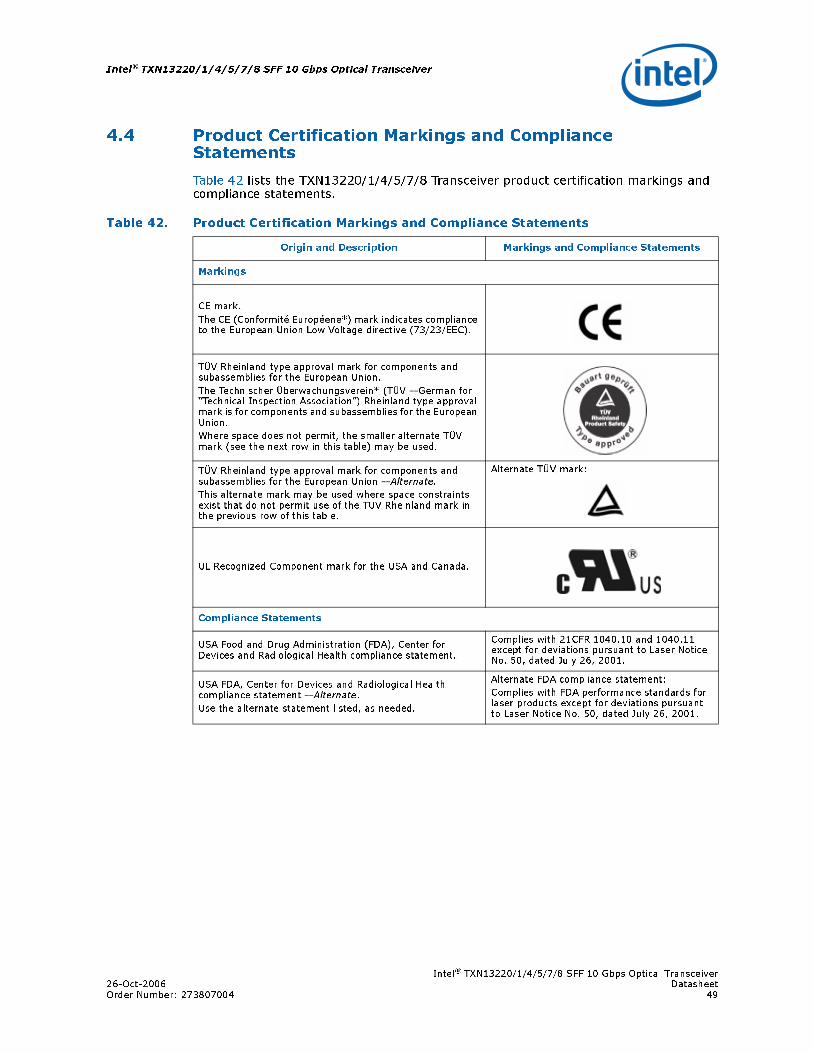
Intel® TXN13220/1/4/5/7/8 SFF 10 Gbps Optical Transceiver26-Oct-2006 DatasheetOrder Number: 273807004 49
Intel® TXN13220/1/4/5/7/8 SFF 10 Gbps Optical Transceiver
4.4 Product Certification Markings and Compliance Statements
Table 42 lists the TXN13220/1/4/5/7/8 Transceiver product certification markings and compliance statements.
Table 42. Product Certification Markings and Compliance Statements
Origin and Description Markings and Compliance Statements
Markings
CE mark.
The CE (Conformité Européene*) mark indicates compliance to the European Union Low Voltage directive (73/23/EEC).
TÜV Rheinland type approval mark for components and subassemblies for the European Union.
The Technischer Überwachungsverein* (TÜV – German for “Technical Inspection Association”) Rheinland type approval mark is for components and subassemblies for the European Union.
Where space does not permit, the smaller alternate TÜV mark (see the next row in this table) may be used.
TÜV Rheinland type approval mark for components and subassemblies for the European Union – Alternate.
This alternate mark may be used where space constraints exist that do not permit use of the TUV Rheinland mark in the previous row of this table.
Alternate TÜV mark:
UL Recognized Component mark for the USA and Canada.
Compliance Statements
USA Food and Drug Administration (FDA), Center for Devices and Radiological Health compliance statement.
Complies with 21CFR 1040.10 and 1040.11 except for deviations pursuant to Laser Notice No. 50, dated July 26, 2001.
USA FDA, Center for Devices and Radiological Health compliance statement – Alternate.
Use the alternate statement listed, as needed.
Alternate FDA compliance statement:
Complies with FDA performance standards for laser products except for deviations pursuant to Laser Notice No. 50, dated July 26, 2001.
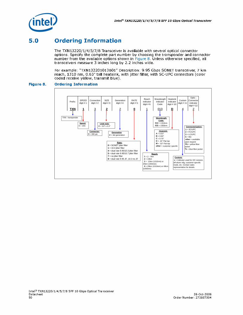
Intel® TXN13220/1/4/5/7/8 SFF 10 Gbps Optical Transceiver
Intel® TXN13220/1/4/5/7/8 SFF 10 Gbps Optical TransceiverDatasheet 26-Oct-200650 Order Number: 273807004
5.0 Ordering Information
The TXN13220/1/4/5/7/8 Transceiver is available with several optical connector options. Specify the complete part number by choosing the transponder and connector number from the available options shown in Figure 8. Unless otherwise specified, all transceivers measure 3 inches long by 2.2 inches wide.
For example: “TXN132201013B01” Description: 9.95 Gbps SONET transceiver, 7 km reach, 1310 nm, 0.63" tall heatsink, with jitter filter, with SC-UPC connectors (color coded receive yellow, transmit blue).
Figure 8. Ordering Information
Prefix:SPEED digit # 1:
Connection digit # 2:
SIZE digit # 3:
Generation digit # 4:
RATE digit # 5:
Reach indicator digit # 6:
Wavelength indicator Code:
Heatsink indicator
digit # 10:
Custom digit # 11:
Optic - Connector indicator digit # 12:
TXN 1 3 2 2 0 1 013 D 4 2
TXN - transponder
Speed: 1 = 10G
CASE SIZE: 2 = 3.0" x 2.2"
Generation 2 = 3rd generation
Rate: 0 = SONET jitter filter 1 = 10.3 jitter filter 4 = dual rate 9.95/10.3 jitter filter 5 = dual rate 9.95/10.7 jitter filter 7 = no jitter filter 8 = dual rate 9.95 JF, 10.3 no JF
Connector: 3 = 300 pin
Reach: 1 = 2 - 7km 2 = 10km 3 = 12km (1310nm) or 25km (1550nm) 4 = 20km (1310nm) or 40km (1550nm)
Wavelength Code:
013 = 1310nm015 = 1550nm
Heatsink: A = 0.53" B = 0.60" C = 0.70" D = .43" Flat top M = .53" Flat top other = customer specific
Connectorization: 1 = SC/UPC 2 = FC/UPC 3 = LC/UPC 5 = MU other = available upon request Rx = yellow fiber jacketTx = blue fiber jacket
Custom: x = Indicator used for I2C revision, off-shore mfg, customer specific mods, etc. Contact sales representative for details.
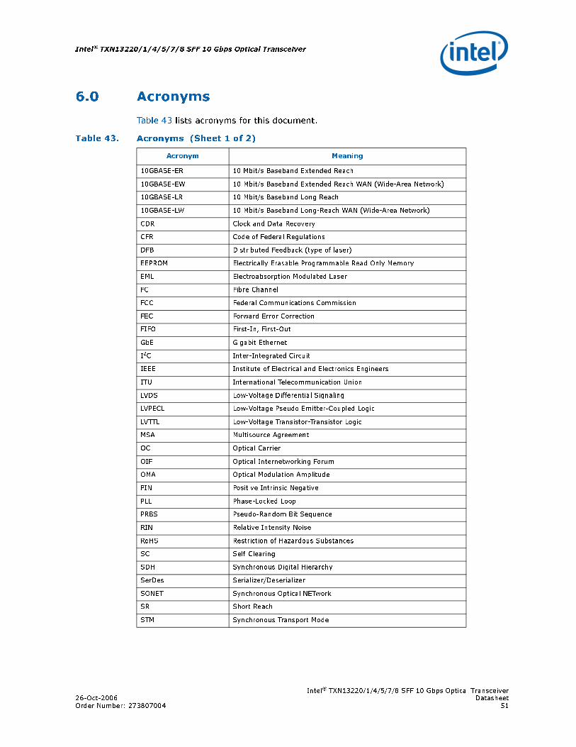
Intel® TXN13220/1/4/5/7/8 SFF 10 Gbps Optical Transceiver26-Oct-2006 DatasheetOrder Number: 273807004 51
Intel® TXN13220/1/4/5/7/8 SFF 10 Gbps Optical Transceiver
6.0 Acronyms
Table 43 lists acronyms for this document.
Table 43. Acronyms (Sheet 1 of 2)
Acronym Meaning
10GBASE-ER 10 Mbit/s Baseband Extended Reach
10GBASE-EW 10 Mbit/s Baseband Extended Reach WAN (Wide-Area Network)
10GBASE-LR 10 Mbit/s Baseband Long Reach
10GBASE-LW 10 Mbit/s Baseband Long-Reach WAN (Wide-Area Network)
CDR Clock and Data Recovery
CFR Code of Federal Regulations
DFB Distributed Feedback (type of laser)
EEPROM Electrically Erasable Programmable Read Only Memory
EML Electroabsorption Modulated Laser
FC Fibre Channel
FCC Federal Communications Commission
FEC Forward Error Correction
FIFO First-In, First-Out
GbE Gigabit Ethernet
I2C Inter-Integrated Circuit
IEEE Institute of Electrical and Electronics Engineers
ITU International Telecommunication Union
LVDS Low-Voltage Differential Signaling
LVPECL Low-Voltage Pseudo Emitter-Coupled Logic
LVTTL Low-Voltage Transistor-Transistor Logic
MSA Multisource Agreement
OC Optical Carrier
OIF Optical Internetworking Forum
OMA Optical Modulation Amplitude
PIN Positive Intrinsic Negative
PLL Phase-Locked Loop
PRBS Pseudo-Random Bit Sequence
RIN Relative Intensity Noise
RoHS Restriction of Hazardous Substances
SC Self-Clearing
SDH Synchronous Digital Hierarchy
SerDes Serializer/Deserializer
SONET Synchronous Optical NETwork
SR Short Reach
STM Synchronous Transport Mode
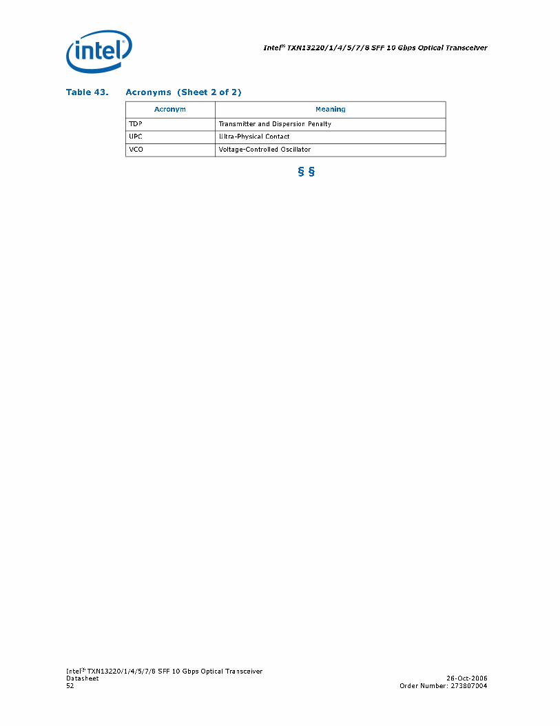
Intel® TXN13220/1/4/5/7/8 SFF 10 Gbps Optical Transceiver
Intel® TXN13220/1/4/5/7/8 SFF 10 Gbps Optical TransceiverDatasheet 26-Oct-200652 Order Number: 273807004
§ §
TDP Transmitter and Dispersion Penalty
UPC Ultra-Physical Contact
VCO Voltage-Controlled Oscillator
Table 43. Acronyms (Sheet 2 of 2)
Acronym Meaning