“digital coherent transceiver for optical communications ... · 1 universitat politÈcnica de...
TRANSCRIPT

1
UNIVERSITAT POLITÈCNICA DE CATALUNYA
“Digital coherent transceiver for optical communications.
From Design to Implementation”
-Master Thesis-
Esdras Anzuola Valencia
February 2012

2
3
“Digital coherent transceiver for optical communications. From Design to Implementation “
Author: Esdras Anzuola Valencia
Director: Aniceto Belmonte Molina
Tutor: Aniceto Belmonte Molina
Departament of Communication and Signal Theory
Technical University of Catalonia (UPC)
February 2012

4

5
Keywords
Coherent Detection, Optical Communications, Phase Shift Keying, Shot Noise, Phase
estimation, Frequency estimation.
Abstract
Recent coherent optical communication systems address modulation and
detection techniques for high spectral efficiency and robustness against transmission
impairments. As a consequence of this technical reality and its potential achievements,
the proposed objective of this project is to develop and demonstrate the coherent
optical infrastructure and signal processing to produce robust high-capacity links over
the 1.5-micron spectral band.
In this project we analyze the theoretical models of optical coherent
communication systems as well as the front-end arquitectures used to implement them.
Key concepts as balanced photo detection and quantum limit are explained and
studied. Complex modulation schemes maximize spectral efficiency and power
efficiency by encoding information in two degrees of freedom. Homodyne and
heterodyne downconvertion are shown to be linear processes that can fully recover the
received signal field. When optical downconverted signals are sampled, compensation
of transmission impairments can be performed using digital signal processing (DSP).
Clock recovery, frequency offset compensation and phase offset compensation
algorithms are studied and their performance is shown.
Based on the theory analyzed, an optical coherent transceiver is designed using
commercially available devices. A system and device characterization is performed.
Implementation effects as bandwidth limitations, laser source deviation and different
noise sources are studied. Modulation and demodulation impairments introduced by
real devices are analyzed in order to evaluate their penalization over the signal quality
at the receiver. The experimental set-up is then implemented and parameterized. The
system performance is validated and the receiver robustness is tested under the
presence of additive white gaussian noise (AWGN).

6

7
Chapter 1. Introduction…………………………………………………………………………………………………………13
1.1. Introduction…………………………………………………………..……………………………………………13 1.2. Motivation and thesis objectives …………………………………………………………………………16 1.3. Thesis organization ……………………………………………………………………………………………..17
Chapter 2. Basic concepts of optical coherent systems………………………………………………………….19
2.1. Optical hybrids and balanced photo detection……………………………………………………..20 2.2. Generic block system for optical coherent systems………………………………………………22 2.3. Homodyne detection…………………………………………………………………………………………..24 2.4. Heterodyne detection…………………………………………………………………………………………..27 2.5. Modulation formats…………………………………………………………………………………………….30
Chapter 3. Design of a digital coherent system……………………………………………………………………..33
3.1. Digital system overview……………………………………………………………………………………….33 3.2. Digital transmitter……………………………………………………………………………………………….34
3.3. Digital receiver…………………………………………………………………………………………………….35 3.3.1. Carrier frequency estimator………………………………………………………………….36 3.3.2. Clock recovery…………..………………………………………………………………………….38 3.3.3. Phase offset compensation…………………………………………………………………..39 3.4. System performance evaluation block…………………………………………………………………41
Chapter 4. Experimental set-up……………………………………………………………………………………………..38 4.1. System arquitecture…………………………………………………………………………………………….43 4.1.1. Optical transmitter……………………………………………………………………………….44 4.1.2. Optical receiver……………………………………………………………………………………45 4.2. Device Characterization……………………………………………………………………………………….47 4.3. Implementation limits and impairment effects……………………………………………………54 4.3.1. Bandwidth limitations………………………………………………………………………….54 4.3.2. Laser line width effects…………………………………………………………………………56 4.3.3. Central frequency laser deviation and path difference fading………………57 4.3.4. Modulation imbalance factors……………………………………………………………..60 4.3.5. Effects of asymmetric hybrids………………………………………………………………62 4.4. System parameters ……………………………………………………………………………………….…….66 Chapter 5. System validation ………………………………………………………………………………………………..69 Chapter 6. Conclusions and future work………………………………………………………………………………..77 Bibliography…………………………………………………………………………………………………………………………..81 Appendix………………………………………………………………………………………………………………………………..85

8

9
GLOSSARY
Analog- to-Digital Converter, ADC:
An analog-to-digital converter is a device that converts continuous signals to discrete
digital numbers.
Balanced detection:
A balanced detector, or balanced receiver, is a device that measures the difference in
the intensity of two laser beams. It is a part of a receiver front-end architecture that
provides better power efficiency for the receiver.
Band-Pass Filter, BPF:
A band-pass filter is a device that passes frequencies within a certain range and rejects
(attenuates) frequencies outside that range.
Birefringence:
The double refraction of light in a transparent, molecularly ordered material, which is
manifested by the existence of orientation-dependent differences in refractive index.
Bit Error Rate, BER:
Number of erroneous bit per transmitted bits.
Bit Rate, Rb:
The number of bits transmitted per unit of time.
Coherence Time:
The time over which a propagating wave (especially a laser) may be considered
coherent. In other words, it is the time interval within which its phase is, on average,
predictable.
Digital Signal Processing, DSP:
The group of numerical techniques that treat a digital signal. These techniques are very
useful because of their stability due to error detection and correction and their reduced
vulnerability to noise. In the design of the digital coherent receiver DSP is used for
compensation of chromatic dispersion, polarization mode dispersion and tracking the
phase of the received signal.

10
Direct Detection Receiver, DD Receiver:
A receiver that works converting optical power directly to electrical domain. These
kinds of detectors are not able to recover the information on the phase of the optical
signal.
Intersymbol Interference, ISI:
The overlapping between symbols, in which one symbol interferes with subsequent
symbols due to a distortion in the received signal that causes the spread of the
symbols. In optical communication the distortion that causes this effect is dispersion.
Local Oscillator, LO:
Laser located in the receiver. Its lightwave is mixed with the incoming signal in the
coherent optical receiver. The mixing lets to obtain the phase of the received signal
Mach-Zender modulator, MZ modulator:
External optical modulator able to modulate phase or and amplitude of an optical
lightwave.
Optical Coherent Detection Receiver:
A receiver that mixes the incoming optical signal with a local optical source lightwave
before converting the signal into electrical domain.
Optical Coupler:
A passive device for branching or coupling an optical signal. Generally, a coupler is
centralized by joining the two fibers together so that the light can pass from the sender
unit to the two receivers, or else it can be made by juxtaposing the two "receiver" fibers
which will then be aligned and positioned so as to be facing the "sender" fiber. In our
design the optical coupler is used to mix the incoming lightwave and the local oscillator
lightwave.
Phase shifter:
Passive device that introduces a delay into an optic path. The phase delay can be fixed
or simply adjusted with a controllable voltage.

11
Phase Diversity Receiver:
A coherent receiver front-end architecture that is able to extract phase information from
the incoming signal by mixing it with a local oscillator signal and it is independent of the
phase difference between them.
Quantum Limit:
A physical low bound for the BER that an optical can achieve due to the quantum
nature of light. In optics, the quantum limit is imposed by the shot noise that occurs
when a sufficient small number of photons generate an occurrence of independent and
significant random events described by a Poisson distribution.
Responsivity of photodiode, R:
A parameter of the photodiode than represents the ability of the device to generate an
electron hole when light hit its surface.
Spectral Efficiency:
A concept that refers to the information bit rate that can be transmitted over a given
bandwidth.
Shot Noise:
A fundamental noise mechanism responsible for current fluctuations in all optical
receivers even when the incident optical power Pin is constant. It is a manifestation of
the fact than an electric current consists of a stream of electrons that are generated at
random times.
Thermal Noise:
A variable current generated by the photodiode due to the fact that, at a finite
temperature, electrons move randomly in any conductor. Random thermal motion of
electrons in a resistor manifests as a fluctuating current even in the absence of an
applied voltage. Thermal noise sets a fundamental lower limit to what can be
measured.

12

13
Chapter 1
1.1. Introduction
In this thesis an optical coherent communication system is designed and
implemented. These types of systems have some advantages over others based on
direct detection, which have been used historically in optical communications. One of
the properties of a coherent receiver is that it provides the possibility of using digital
signal processing (DSP) once the signal has been detected. Through these methods
we are able to compensate the impairments of optical coherent communications as
clock recovery, carrier frequency and phase estimation, modulation imbalance
impairments or additive Gaussian noise.
In optical communications there are two major kinds of detectors: direct
detection and coherent detection. The direct detection is so named because the
incoming signal is detected directly with the photodiode which is the element in charge
of converting the optical power into a current (Figure 1). These detectors can only obtain
the amplitude of the signal, losing its phase. With the direct detection only the
amplitude of the signal can be obtained, losing its phase.

14
Figure 1. Direct detection receiver scheme. The incoming optical signal Es(t )is band pass filtered Efs(t) and its
intensity is directly detected with a photodiode, which converts the optical power into a current I(t).
On other hand, for coherent detection the incoming light wave is mixed with
other light beam coming from the local oscillator (LO) before being detected by the
photodiode (Figure 2). The signal detected by the coherent detector preserves both the
amplitude and the phase of the signal.
Figure 2. Coherent receiver generic scheme. The coherent detector (CohD RX) uses a local oscillator signal (Elo) to convert the optical signal into a currents. These current or set of currents are sent to the Digital Receiver, which is responsible for the demodulation process. The CohD together with the Digital Receiver is called Digital Coherent
Receiver.
For coherent detection there are two basic schemes depending on how the
downconvertion from optical frequencies to baseband frequencies is performed. These
schemes are called heterodyne detection and homodyne detection.
In homodyne detection the local oscillator is tuned so that the output of the
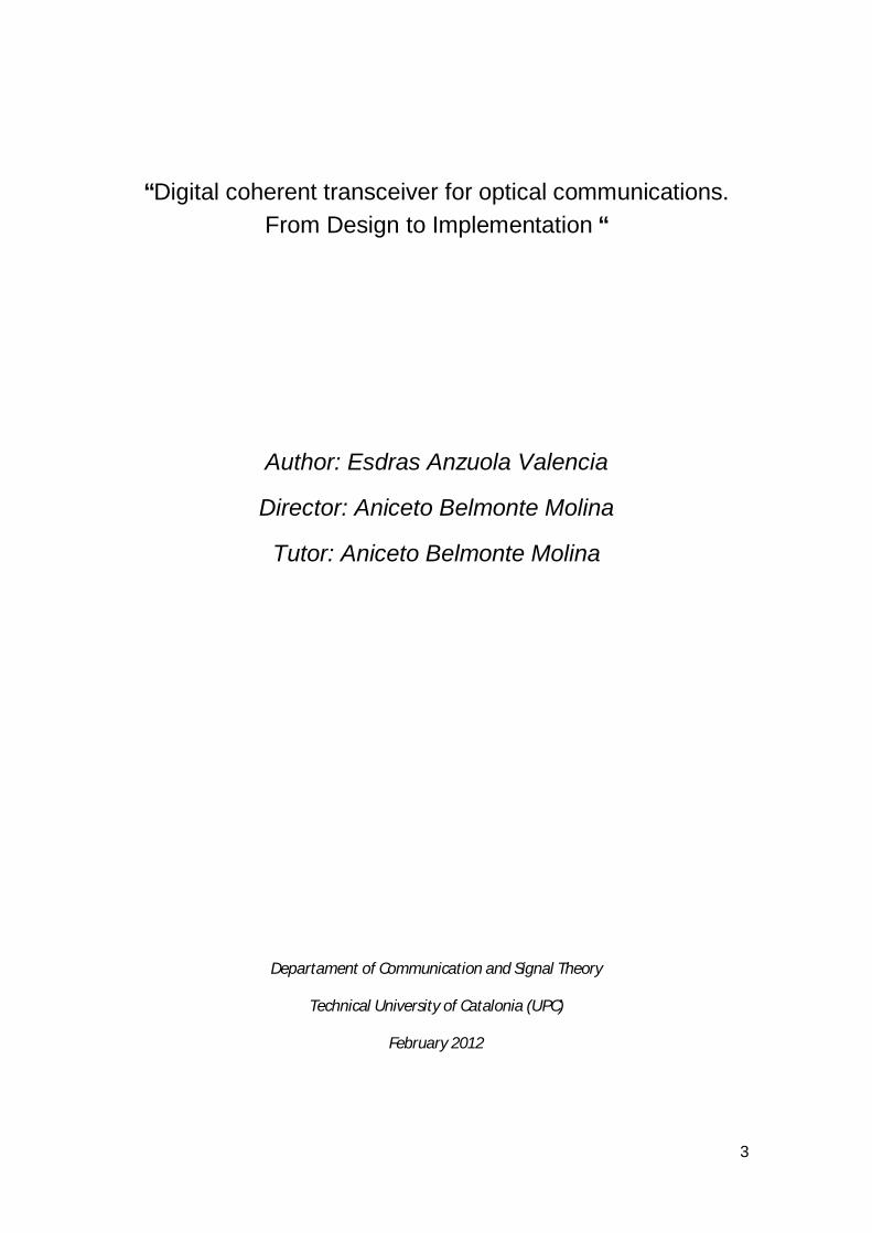
optical mixer is at baseband frequencies (Figure 3)
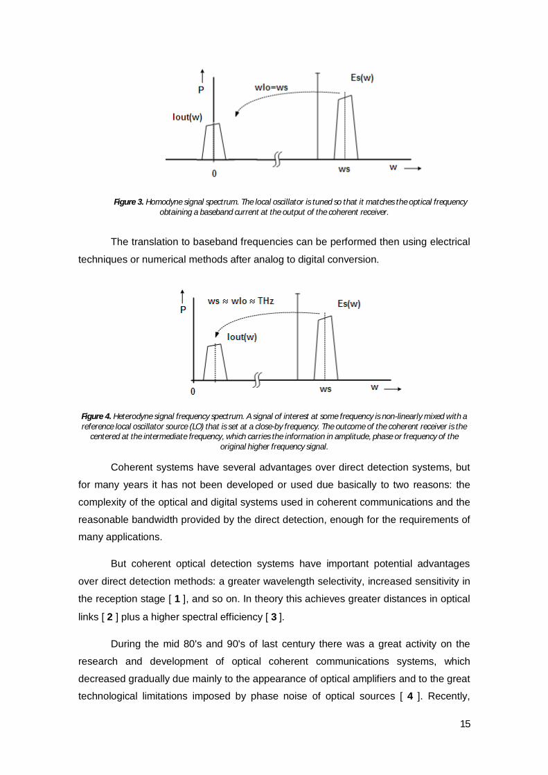
In heterodyne detection, a signal of interest at some frequency is non-linearly
mixed with a reference local oscillator source (LO) that is set at a close-by frequency.
The outcome is centered at the difference frequency, which carries the information in
amplitude, phase or frequency of the original higher frequency signal, but oscillating at
intermediate carrier frequency (Figure 4) which can be handled easily.
15
Figure 3. Homodyne signal spectrum. The local oscillator is tuned so that it matches the optical frequency obtaining a baseband current at the output of the coherent receiver.
The translation to baseband frequencies can be performed then using electrical
techniques or numerical methods after analog to digital conversion.
Figure 4. Heterodyne signal frequency spectrum. A signal of interest at some frequency is non-linearly mixed with a reference local oscillator source (LO) that is set at a close-by frequency. The outcome of the coherent receiver is the
centered at the intermediate frequency, which carries the information in amplitude, phase or frequency of the original higher frequency signal.
Coherent systems have several advantages over direct detection systems, but
for many years it has not been developed or used due basically to two reasons: the
complexity of the optical and digital systems used in coherent communications and the
reasonable bandwidth provided by the direct detection, enough for the requirements of
many applications.
But coherent optical detection systems have important potential advantages
over direct detection methods: a greater wavelength selectivity, increased sensitivity in
the reception stage [ 1 ], and so on. In theory this achieves greater distances in optical
links [ 2 ] plus a higher spectral efficiency [ 3 ].
During the mid 80's and 90's of last century there was a great activity on the
research and development of optical coherent communications systems, which
decreased gradually due mainly to the appearance of optical amplifiers and to the great
technological limitations imposed by phase noise of optical sources [ 4 ]. Recently,

16
however, has revived the interest in such systems [ 5 ], on a quest to increase the
capacity and in view of new technological developments in the area of optical sources,
balanced photoreceptors, digital processing of high-speed signals [ 6 ] and applying
innovative techniques of coding and synchronization. The current trend in coherent
optical communications is primarily oriented to the digital processing and compensation
of phase perturbations in optical systems with phase modulation [ 7 ][ 8 ].
1.2. Motivation and Thesis Objectives
It has been shown that there are many advantages that coherent reception
can bring to optical communications [ 2 ]. The present project has as its main
objective the design, implementation and test of an optical coherent transceiver.
The following objectives are targeted to be accomplished in this project:
Describe and study the basic concepts involved in coherent communications.
Analyze and model the optical coherent communication system as well as the
front-end arquitectures used to implement the homodyne and heterodyne
detection methods.
Study the theoretical limits and performance of an optical coherent
communication system using different modulation formats.
Implementation and performance study of the different compensation
techniques needed in a real optical coherent receiver such as: o Clock recovery o Frequency offset estimation o Phase offset estimation
Design of an experimental set-up in order to implement an optical coherent
communication system using commercially available devices.
Characterize the physical devices involved on the system, as well as measure
and quantify the impairments introduced by these non-ideal devices.
Study the implementation limits introduced by the devices used as: o Bandwidth limitations o Laser source deviation. o Modulation imbalance factors o Asymmetric demodulation factors.
Implementation of an optical coherent communication system.
17
Test our communication system and study its performance in the presence
of additive white gaussian noise (AWGN).
1.3. Thesis Organization
In Chapter 2 the basics of optical coherent communications systems will be
described, explaining the main concepts of homodyne and heterodyne detection, and
exposing the theory and the main differences between the two coherent methods. Also
some concepts about modulation formats, shot noise and quantum limit will be
introduced.
In Chapter 3, the coherent system algorithms will be studied. We will indicate
the compensating modules that must be present on a real coherent system as well as
their theoretical fundamentals. The performance of each module will be tested in
different scenarios in order to characterize their response in real systems.
In Chapter 4 we will describe the experimental set-up, showing the system
overview, device characterization, hardware limitations and impairments and system
parameters.
In Chapter 5 we present our analysis results. It is dedicated to study each
module involved in the system. We will test their individual properties and we will
characterize the whole system performance in different scenarios.
In Chapter 6 the conclusions obtained are presented and the ideas for future
work on coherent systems are extracted from the project.

18

19
Chapter 2
Chapter 2 – Basic Concepts of Optical Coherent Systems
In this section the basics of coherent detection are explained. Concepts about
homodyne and heterodyne systems as well as their mathematical models are covered.
The different system arquitectures will be shown and we will describe the main
advantages of coherent detection over direct detection methods, such us sensitivity
and system performance.
We will also discuss the modulation formats used for this project, as well as a
brief description of the signal nature and spectrum, in order to better understand effects
explained on further chapters.

20
2.1. Optical Hybrids and Balanced Photo detection
There are two important devices that must be explained before describing how
a coherent system is designed. First, an optical hybrid is generally described as a
device that is able to mix light beams. Second, balanced photo detectors are devices
which optimize the translation of optical fields into currents.
2.1.1. Optical Hybrids
In coherent systems we need an optical hybrid in order to mix an optical signal
with a local oscillator source. The simplest hybrid is a 3dB coupler, also called 50/50
beam splitter or 1800 hybrid, This device can be modeled as shown in Figure 5.
1
2
3
4
Ei1(t)
Ei2(t)
Eo1(t)=Ei1(t) +jEi2(t)
Eo2(t)=jEi1(t) +Ei2(t)
Figure 5. Optical 1800 hybrid. Each input field is splitted into two output ports. A phase shift of 180 degrees is introduced in one of the branches
Here, each one of the two input fields is splitted into the two output ports and a phase
shift of 180 degrees is introduced in one of the branches. Mathematically this device
can be modeled as:
퐸퐸 =
1√2
1 푗푗 1
퐸푖퐸
(2. 1)
where 퐸 , 퐸 [V/m] are the input fields and 퐸 ,퐸 [V/m] are the output fields. Its
diagram is shown in figure 5.
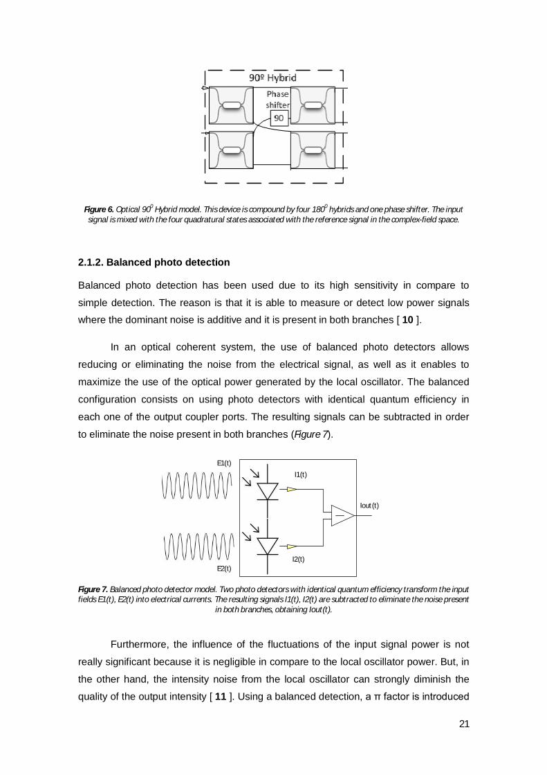
A 90° optical hybrid is a six-port device that is used for coherent signal demodulation
(Figure 6). It would mix the incoming signal with the four quadratural states associated
with the reference signal in the complex-field space.
21
Figure 6. Optical 900 Hybrid model. This device is compound by four 1800 hybrids and one phase shifter. The input signal is mixed with the four quadratural states associated with the reference signal in the complex-field space.
2.1.2. Balanced photo detection
Balanced photo detection has been used due to its high sensitivity in compare to
simple detection. The reason is that it is able to measure or detect low power signals
where the dominant noise is additive and it is present in both branches [ 10 ].
In an optical coherent system, the use of balanced photo detectors allows
reducing or eliminating the noise from the electrical signal, as well as it enables to
maximize the use of the optical power generated by the local oscillator. The balanced
configuration consists on using photo detectors with identical quantum efficiency in
each one of the output coupler ports. The resulting signals can be subtracted in order
to eliminate the noise present in both branches (Figure 7).
E1(t)
E2(t)
I1(t)
I2(t)
Iout(t)
Figure 7. Balanced photo detector model. Two photo detectors with identical quantum efficiency transform the input fields E1(t), E2(t) into electrical currents. The resulting signals I1(t), I2(t) are subtracted to eliminate the noise present
in both branches, obtaining Iout(t).
Furthermore, the influence of the fluctuations of the input signal power is not
really significant because it is negligible in compare to the local oscillator power. But, in
the other hand, the intensity noise from the local oscillator can strongly diminish the
quality of the output intensity [ 11 ]. Using a balanced detection, a π factor is introduced

22
in one of the branches, so that the common signal is subtracted and the differential
signal is amplified.
Also, in a simple photo detector a significant part of the power is lost. In the
balanced photo detector almost all the power is exploited, increasing the receptor
sensitivity in compare to a simple detector [ 12 ].
In practice, the performance of a balanced photo detector is not perfect due to
differences on the detectors responsitivities, electrical path length or other non-
idealities. So the performance is characterized in terms of the CMRR (Common Mode
Rejection Ratio), which is defined as the capacity of attenuate the common terms and
amplify the differential ones [ 13 ].
퐶푀푅푅 = 20log퐴퐴
[푑퐵] (2. 2)
Here 퐴 is the differential gain and 퐴 is the common gain.
2.2. Generic Block System for Coherent Communications
The most basic idea on a coherent system is that, in the reception stage, the
modulated optical signal is mixed with a local oscillator. Figure 2.1 shows the basic
block diagram of a coherent system.
Figure 8. Basic Coherent System. Transmitter: A light coming from the laser source is shaped at the modulator by an electrical signal coming from the signal generator obtaining a transmitted optical signal 푬푺(풕). The signal is sent through the channel and mixed with the light generated at the local oscillator 푬푳푶(풕) using an optical Hybrid. The output of the mixer is translated into a current, which after A/D
conversion is converted to data by the demodulator. In transmission, the light coming from the laser source is shaped by an electrical signal
by the modulator. This electrical signal is generated based on the data to be
transmitted and on the modulation format used. The transmitted optical signal 퐸 (푡)
[푉/푚] can be represented as:
퐸 (푡) = 푃 ∗ 푒 ∅ ∗ 푒 ∗ (2. 3)
23
where 푃 [푊],푤 [푟푎푑/푠]and∅푺[푟푎푑] are the power, frequency and phase of the optical
signal, respectively.
The signal is sent through the channel and in the receiver stage is mixed with
the light generated by the local oscillator (LO), which can be represented as:
퐸 (푡) = 푃 ∗ 푒 ∅ ∗ 푒 ∗ (2. 4)
Here, 푃 [푊],푤 [푟푎푑/푠]and∅푳푶[푟푎푑] are the power, frequency and phase of the local
oscillator signal [ 9 ].
Both signals are mixed in an optical hybrid and its outputs are sent to the digital
receiver. As we have mentioned in the introduction, depending on the relationship
between the optical frequencies of the signal and the local oscillator we will have two
different demodulation schemes. In heterodyne detection 푤 ≠ 푤 [rad/s] and the
downconvertion is performed in two separated steps. The coherent detector is a 1800
hybrid which outputs are converted into a current 퐼 (푡) [A] by one single balanced
photo detector. The output intensity is centered at a frequency 푤 = 푤 −푤
[rad/s].This current is digitally processed and the baseband conversion is performed by
a digital downconvertion. The resulting basebands currents are 퐼 , (푡) [A] and
퐼 , (푡) [A], which correspond to the in-phase and quadrature branches of a complex
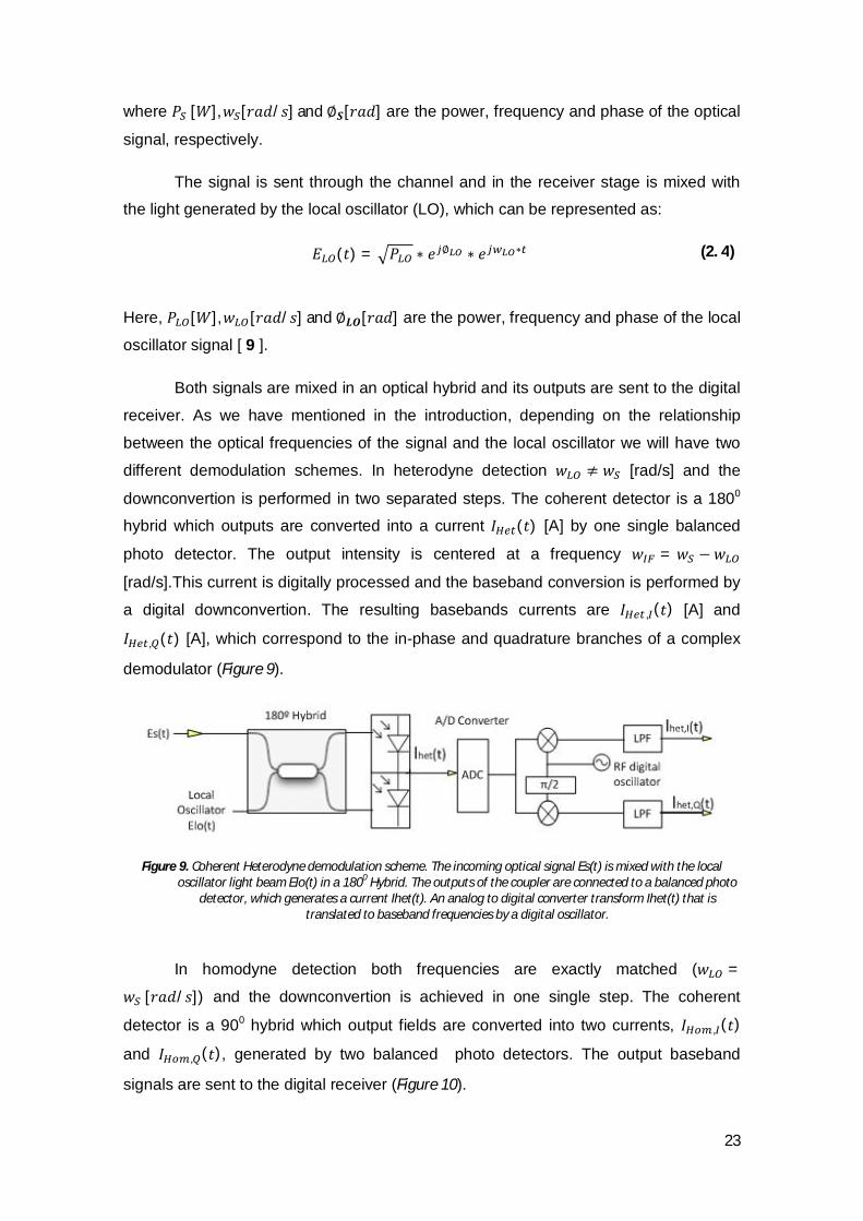
demodulator (Figure 9).
Figure 9. Coherent Heterodyne demodulation scheme. The incoming optical signal Es(t) is mixed with the local
oscillator light beam Elo(t) in a 1800 Hybrid. The outputs of the coupler are connected to a balanced photo detector, which generates a current Ihet(t). An analog to digital converter transform Ihet(t) that is
translated to baseband frequencies by a digital oscillator.
In homodyne detection both frequencies are exactly matched (푤 =
푤 [푟푎푑/푠]) and the downconvertion is achieved in one single step. The coherent
detector is a 900 hybrid which output fields are converted into two currents, 퐼 , (푡)
and 퐼 , (푡), generated by two balanced photo detectors. The output baseband
signals are sent to the digital receiver (Figure 10).

24
Figure 10. Coherent Homodyne demodulation scheme. The incoming optical signal Es(t) is mixed with the local oscillator light beam Elo(t) in a 900 Hybrid, which is composed by four 1800 hybrids and a 900 phase shifter. The outputs of the hybrid are connected to two balanced photo detectors, which generate two baseband currents
퐼 , (푡) and 퐼 , (푡). An analog to digital converter transform both currents into a digital signal, which can be processed by the digital demodulator.
Both schemes are able to demodulate correctly the transmitted signal but they
accomplish the task in two different ways, which means that after this point we will
have to study both systems separated.
2.3. Homodyne detection
In this coherent detection technique, the local oscillator frequency 푤 is chosen
to match exactly the information signal frequency.
The incoming optical signal 퐸 (푡) [V/m] is mixed in the receiver with the local
oscillator signal 퐸 (푡) [V/m] using a 90 degrees hybrid. This hybrid is formed by four
hybrids of 1800 and a 90 degrees phase shifter.
90
Es(t)
Elo(t)
Ihom,I(t)
Ihom,Q(t)
90º Hybrid
1
2
3
4
8
7
5
6
9
10
Figure 11. Coherent homodyne optical downvertion scheme. The incoming optical signal Es(t) and local oscillator signal Elo(t) enter the 90º hybrid through ports 1 and 2. The output fields of the hybrid, corresponding to ports 5, 6, 9
and 10, are translated into the baseband currents 푰풉풐풎,푰(풕) and 푰풉풐풎,푸(풕) by two balanced photo detectors.
25
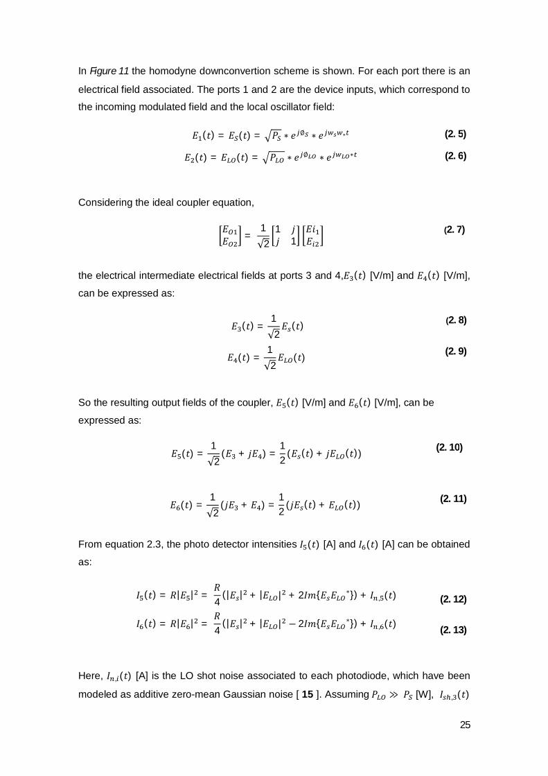
In Figure 11 the homodyne downconvertion scheme is shown. For each port there is an
electrical field associated. The ports 1 and 2 are the device inputs, which correspond to
the incoming modulated field and the local oscillator field:
퐸 (푡) = 퐸 (푡) = 푃 ∗ 푒 ∅ ∗ 푒 ∗ (2. 5)
퐸 (푡) = 퐸 (푡) = 푃 ∗ 푒 ∅ ∗ 푒 ∗ (2. 6)
Considering the ideal coupler equation,
퐸퐸 =
1√2
1 푗푗 1
퐸푖퐸 (2. 7)
the electrical intermediate electrical fields at ports 3 and 4,퐸 (푡) [V/m] and 퐸 (푡) [V/m],
can be expressed as:
퐸 (푡) =1√2
퐸 (푡) (2. 8)
퐸 (푡) =1√2
퐸 (푡) (2. 9)
So the resulting output fields of the coupler, 퐸 (푡) [V/m] and 퐸 (푡) [V/m], can be
expressed as:
퐸 (푡) =1√2
(퐸 + 푗퐸 ) =12
(퐸 (푡) + 푗퐸 (푡)) (2. 10)
퐸 (푡) =1√2
(푗퐸 + 퐸 ) =12
(푗퐸 (푡) + 퐸 (푡)) (2. 11)
From equation 2.3, the photo detector intensities 퐼 (푡) [A] and 퐼 (푡) [A] can be obtained
as:
퐼 (푡) = 푅|퐸 | = 푅4
(|퐸 | + |퐸 | + 2퐼푚{퐸 퐸 ∗}) + 퐼 , (푡)
(2. 12)
퐼 (푡) = 푅|퐸 | = 푅4
(|퐸 | + |퐸 | − 2퐼푚{퐸 퐸 ∗}) + 퐼 , (푡) (2. 13)
Here, 퐼 , (푡) [A] is the LO shot noise associated to each photodiode, which have been
modeled as additive zero-mean Gaussian noise [ 15 ]. Assuming푃 ≫푃 [W], 퐼 , (푡)
26
[A] has a two sided psd of 푆 , (푓) = 푞푅 [ ], where q is the elementary charge of
an electron and 푅 [A/W] is the photo detector responsivity. This fact means that we are
working on the shot noise limited scenario, where we can neglect other noise sources
as thermal noise and dark current photo detector noise [ 14 ].
Using the same procedure, we can obtain the electrical fields at the
intermediate ports 7 and 8 of the device.
퐸 (푡) =푗√2
∗ 푗퐸 (푡) = −1√2
∗ 퐸 (푡) (2. 14)
퐸 (푡) =푗√2
퐸 (푡) =푗√2
퐸 (푡) (2. 15)
Applying equation 2.9, the output electrical fields at ports 9 and 10 can be expressed
as:
퐸 (푡) =1√2
(퐸 + 푗퐸 ) =1√2
−1√2
퐸 (푡) −1√2
퐸 (푡) (2. 16)
퐸 (푡) =1√2
(푗퐸 + 퐸 ) =1√2
−푗√2
퐸 (푡) +푗√2
퐸 (푡) (2. 17)
From these equations we can obtain the intensities (푖(푡) = |퐸| ) generated by the
photo detectors placed at the output of ports 9 and 10:
퐼 (푡) = 푅|퐸 | = 푅4
(|퐸 | + |퐸 | + 퐸 퐸 ∗ + 퐸 퐸 ∗) + 퐼 , (푡)
=푅4
(|퐸 | + |퐸 | + 2푅푒{퐸 퐸 ∗}) + 퐼 , (푡)
(2. 18)
퐼 (푡) = 푅|퐸 | = 푅4
(|퐸 | + |퐸 | − 퐸 퐸 ∗ − 퐸 퐸 ∗) + 퐼 , (푡)
=푅4
(|퐸 | + |퐸 | − 2푅푒{퐸 퐸 ∗}) + 퐼 , (푡)
(2. 19)
Using balanced detection at the output of both couplers, 퐼 , (푡) [A] and 퐼 , (푡) [A]
can be expressed as:
퐼 , (푡) = 푅 푃 푃 ∗ 푐표푠[(∅ − ∅ )] + 퐼 , (푡) (2. 20)
퐼 , (푡) = 푅 푃 푃 ∗ 푠푖푛[(∅ − ∅ )] + 퐼 , (푡) (2. 21)
27
where 퐼 , (푡) [A] and 퐼 , (푡) [A], considering equal responsivities and independent
noise for each photodiode, are white zero-mean additive noises with two-sided PSD of
[ 15 ]:
푆 (푓) = 푞푅
푃2[퐴퐻푧
] (2. 22)
Since it can be shown that thermal noise is always negligible compared to shot
noise [ 9 ], and that we will not consider ASE noise in our system (no optical
amplification will be used), we have neglected this terms in equations (2. 20) and (2. 21)
Finally, the two resulting intensities are the in-phase and quadrature
components of the transmitted signal, which allows the use of complex modulation
formats and the associated bandwidth gain. As we can see, the intensities on both
branches are directly proportional to the local oscillator power, which allows improving
the SNR at the receiver and reach the shot noise limit [ 9 ].
In the other hand, the control of the local oscillator phase ∅ [rad] is needed in
order to extract all the information from the incoming signal. This is because, as we see
in equations (2. 20)(2. 21), the presence of this term will affect directly the output photo
detector currents. This means that an additional module is needed in order to
compensate this effect.
Also the local oscillator optical frequency has to match exactly the signal optical
frequency, condition that introduces strict hardware design requirements. Some of
these problems are avoided using heterodyne detection, which will be discussed in the
next section.
2.4. Heterodyne detection
In heterodyne detection the local oscillator frequency 푤 [푟푎푑/푠] is not
matched with the signal central frequency 푤 [rad/s]so the detected signal is present
around an intermediate frequency 푤 [푟푎푑/푠] (Figure 12).

28
Figure 12. Signal spectrum heterodyne optical downconvertion. The incoming optical signal Es(w) centered at 풘푺 is
translated from optical frequencies (THz) to an intermediate frequency by mixing it with a local oscillator source centered at 풘푳푶. After photo detection, 푰풉풆풕(풘) is obtained.
The equation analysis is based on the demodulation scheme that uses an
optical coupler, which mixes the incoming signal and the local oscillator generated field
(Figure 13).
Figure 13. Coherent Heterodyne optical downconvertion block. The incoming optical signal 푬푺(풕) and the local oscillator signal 푬푳푶(풕) enter the 1800 hybrid using ports 1 and 2 respectively. The output fields 푬ퟑ(풕) and 푬ퟒ(풕),
generated at ports 3 and 4 respectively, are sent to the balanced photo detector obtaining the current 푰풉풆풕(풕).
Using equation (2. 1). and assuming that 퐸 (푡) = 퐸 (푡) and 퐸 (푡) = 퐸 (푡) we obtain:
퐸 (푡) =1√2
(퐸 + 푗퐸 ) = 1√2
(퐸 + 푗퐸 ) (2. 23)
퐼 (푡) = 푅 ∗ |퐸 (푡)| = 푅2
(|퐸 | + |퐸 | + 2퐼푚{퐸 퐸 ∗}) + 퐼 , (푡) (2. 24)
Here, 퐼 , (푡) [A] is the LO shot noise associated to the first photodiode and It has a two
sided PSD of 푆 , (푓) = 푞푅푃 [ ] assuming a shot noise limited scenario. We get
퐼 (푡) [A] using the same analysis:
퐸 (푡) =1√2
(푗퐸 + 퐸 ) =1√2
푗퐸 ∗ 푒 + 퐸 ∗ 푒 (2. 25)

29
퐼 (푡) = 푅 ∗ |퐸 (푡)| = 푅 퐸 (푡) ∗ 퐸∗(푡)
= 푅2
(|퐸 | + |퐸 | + 푗퐸 퐸 ∗ − 푗(퐸 퐸 ∗)∗
= 푅2
(|퐸 | + |퐸 | − 2퐼푚{퐸 퐸 ∗}) + 퐼 , (푡)
(2. 26)
Applying the balanced photo detection:
퐼 (푡) = 퐼 (푡) − 퐼 (푡) = 2푅 ∗ 퐼푚{퐸 퐸 ∗} + 퐼 (푡) (2. 27)
where 퐼 (푡) = 퐼 , (푡) − 퐼 , (푡) is approximated as a zero-mean Gaussian noise.
Assuming that we are working on the shot noise limit, the noise PSD can be expressed
as [ 16 ]:
푆 (푓) = 푞푅(푃 + 푃 )[
퐴퐻푧
] ≅ 푞푅푃 [퐴퐻푧
] (2. 28)
The PSD’s of the two noise processes can be added because they are generated by
different photodiodes, which are independent. Substituting in (2.29), we get:
퐼 (푡) = 2푅 푃 푃 ∗ 푠푖 푛[(푤 푡 + (∅ − ∅ )] + 퐼 (푡) (2. 29)
It is feasible to send information in amplitude, phase and frequency using this signal.
Also, we can still use the local oscillator power to amplify the received signal improving
the SNR. After optical down-conversion to an intermediate frequency, we need an
electrical demodulation in order to extract the I and Q components. For that purpose,
the widely known scheme Figure 14 is used:
Figure 14. Digital demodulation scheme for coherent heterodyne. The input current 푰풉풆풕(풕) is multiplied by a sine signal 푰푹푭(풕) generated by a digital RF oscillator. After low pass filtering, the baseband in-phase (I) current 푰풉풆풕,푰(풕) is generated. To generate the quadrature (Q) current 푰풉풆풕,푸(풕), the incoming current 푰풉풆풕(풕) is multiplied by 푰푹푭(풕)
shifted 흅/ퟐ [rad] and low pass filtering is applied.
Here, the different intensities can be expressed as:
퐼 (푡) = 퐼 ∗ 푠푖푛(푤 푡 + ∅ ) (2. 30)
퐼 , (푡) = 퐼 (푡) ∗ 퐼 (푡) (2. 31)

30
퐼 , (푡) = 퐼 (푡) ∗ 퐼 ∗ 푠푖푛(푤 푡 + ∅ −
휋2
) (2. 32)
Assuming a perfect frequency match between 푤 [rad/s] and 푤 [rad/s] we can
express the resulting baseband signals and after low pass filtering we obtain the
intensities for each branch:
퐼 , (푡) = 푅 푃 푃 퐼 ∗ 푐표푠[(∅ − ∅ − ∅ )] + 퐼 , (푡) (2. 33)
퐼 , (푡) = 푅 푃 푃 퐼 ∗ 푠푖푛[(∅ − ∅ − ∅ )]+퐼 , (푡) (2. 34)
where 퐼 , (푡) [A] and 퐼 , (푡) [A] have a resulting PSD of 푆 (푓) = 푞푅 [ ]. This
means that the resulting baseband signals for the heterodyne case have exactly the
same expression that the homodyne cases, as well as all the noises have the same
PSD’s. Hence, the heterodyne and the two-quadrature homodyne down converters
have the same performance [ 17 ].
A difference between heterodyne and homodyne down conversion only occurs
when the transmitted signal occupies one quadrature (e.g. 2-PSK) and the system is
LO shot noise limited. This fact enables the use of a single-quadrature homodyne down
converter that uses exactly the same scheme as the heterodyne case, which implies
that the signal term is doubled (four times the power), while the shot noise power is
only increased by two [ 18 ], obtaining a sensitivity improvement of 3 dB compared to
the heterodyne and two-quadrature case.
The main advantage of using a heterodyne optical system is that we are using
only one balanced photo detector and the simple 1800 optical hybrid is used. However,
the photocurrent in the heterodyne case has a larger bandwidth than the homodyne
case due to the fact that the information signal is modulated in an intermediate
frequency. Typically, this frequency 푤 is chosen to be close to the signal bandwidth
(BW), which implies a total required bandwidth of twice the bandwidth for the
heterodyne case. This implies an extra bandwidth requirement, doubling the required
bandwidth of the homodyne case.
2.5. Modulation formats
As we saw in the previous chapter, coherent receivers maintain the phase of
the received signal, so information can be sent in the phase, the frequency or in the
amplitude of the signal. Many studies have been performed and the discussion of

31
the modulation formats has been widely covered. Our objective in this project is to
develop a practical system that offers us the best advantages of a coherent system,
so we need to define the key parameter in order to choose our modulation format.
Typical parameters are the bit-error-rate (BER), sensitivity and spectral
efficiency. Having a look to previous work [ 19 ], [ 20 ], [ 21 ] we obtain the following
results shown in Figure 15.
Figure 15. Sensitivity (photons/bit) VS. Modulation formats.
As we see, PSK and QAM modulation formats exhibit advantages in all the
parameters considered.
Phase-shift keying (PSK) is a digital modulation scheme that conveys data by
changing or modulating the phase of a reference signal. In the case of PSK format the
information is coded on the phase of the optical signal while the amplitude and
frequency are kept constant.
For binary PSK, the phase takes two values: 0 and π depending on the bit
transmitted. The sensitivity of such modulation is even better than the quantum
0
10
20
30
40
50
60
70
80
90
Modulation Formats
Sen
sitiv
ity (p
hoto
ns/b
it)
2-PSKHomodyne
PSKHet-Sync
IM/DDQuantumLimit
FSK - Het-Sync
FSK - Het-aSync
ASKHet-Sync
ASKHom
DPSKHet-Diff
ASKHet-aSync
9
18 20 20
36 36
40
72
80

32
limit. An interesting aspect of PSK modulation is that the optical intensity remains
constant and therefore, the amplitude decision thresholds remain constant.
Figure 16. M-PSK IQ constellations. A) M=2 b) M=4
The use of the PSK format requires that the phase of the optical carrier remains
stable so that the phase information can be extracted at the receiver without
ambiguity; this requirement puts a stringent condition on the tolerable line widths of
the lasers involved. The laser line width can be seen as an additive phase noise,
represented by 휑(푡), at the output of a noise free modulator:
퐸(푡) = 퐴 ∗ cos(푤푡 + ∅ (푡) + 휑(푡))[푊] (2. 35)
where ∅ (푡)[푟푎푑] is the modulated phase and A is the signal amplitude. In order to
be able to extract any phase information we need that 휑(푡)[푟푎푑]fulfill some specific
requirements that will be explained in chapter 4.

33
Chapter 3 – Design of a Digital Coherent System
3.1 Digital System Overview
In order to implement an optical coherent communication system first we need
to study and design the digital transmitter and digital receiver arquitecture, as well as
the methods that will allow us to study the system performance. Based on this
principle, we will generate a digital system that contains:
Digital transmitter, responsible for data and signal generation.
Digital receiver, responsible for impairment compensation and data
demodulation.
Digital control system, responsible for error counting and performance
evaluation.

34
Figure 17. Digital system design overview. The control system receives information from the transmitter and receiver to calculate the system performance
3.2. Digital transmitter
The digital transmitter is the block responsible for data and signal generation.
First, a pseudo-random sequence of data is generated and it will act as the information
message to be transmitted. Then a unique word preamble is added. This preamble is
needed in order to detect the beginning of the message and to design an ambiguity
resolution circuitry at the receiver that will help us with the demodulation (see 3.3). The
data bits are grouped depending on the modulation order (M). Each group of data
generates a particular signal, called symbol, which depends on the modulation format
chosen. In our project complex modulations are of special interest, so at the output of
the signal generator two signals will be produced: the in-phase and quadrature signals.
In the homodyne case these signals will be sent through different output
channels due to their baseband nature (Figure 18). If not, an overlap would be produced
with the consequent lost of information.
Figure 18. Homodyne digital transmitter.
For the heterodyne case the same procedure for data generation is applied, but
instead of sending the data trough different channels, the I and Q branches are
upconverted by multiplying each one of them by the sine and cosine of the selected

35
carrier frequency 푤 [rad/s], respectively. Both branches are then added and the
resulting signal is sent through the channel to the receiver (Figure 19).
Figure 19. Heterodyne Digital transmitter. Signals are generated using the same procedure than in the homodyne case. When the in-phase 푺풊[풏] and quadrature 푺푸[풏] signals are generated, they are multiplied by the cosine and sine of the carrier frequency 풘풄. Both branches are then added and the resulting signal is sent through the channel
to the receiver
In our project we will use no return to zero (NRZ) signaling, which implies that
the generated waveform is suppressed carrier in nature [ 22 ]. The power spectrum of
the baseband signals generated for each branch in the homodyne case is shown in
Figure 20.
Figure 20. Power spectrum of NRZ signaling. Tb is the symbol time and L is the pattern length.
In the heterodyne case the signal spectrum is exactly the same, but centered
around 푤 instead of around the zero frequency.
3.3. Digital Receiver
The demodulation process of a coherent system can be divided into several
major sections (Figure 21). First, since the incoming waveform is suppressed carrier in
nature coherent detection is required. This means that the first action must be recover
the intermediate frequency (heterodyne case) in order to translate the modulated data

36
into the baseband frequencies or compensate any frequency drift between the central
frequency of the signal and the central frequency of the local oscillator (homodyne
case). Next, the input waveform is multiplied by the estimated carrier frequency, which
allows us to derive the clock-synchronization information that will indicate us the
optimal sampling points.
ClockRecovery
Frequency estimation
&compensation
Phase offsetcompensation
SymbolDemodulation
Figure 21. Digital coherent receiver block system.
Once we have the sampled data, we can work with the obtained points to
estimate the phase shift introduced by the constant phase difference between the
transmitter source and the optical and electrical sources at the receiver. After preamble
decoding, the demodulator is able to translate the data into bits, which will be
compared to the transmitted bits in order to get the number of error, obtaining this way
the bit error rate of the system.
3.3.1. Carrier Frequency Estimator
Ideally, the carrier frequency of a system could be parameterized and this block
would be unnecessary. The receiver would know the exact frequency that the
transmitter is using and no error would be produced. In practice, we find that the
received frequency doesn’t match exactly the transmitted frequency. This offset is
generated by the difference between the transmitter and local oscillator laser, as well
as differences in the clock rates between the two systems.
A frequency offset produces a phase shift on the constellation and it introduces
errors, leading in most of the times to a complete loss of the data (Figure 22).

37
Figure 22. Constellation rotations due to frequency drift a) 10 MHz b) 1GHz
The demodulated signal for both heterodyne and homodyne cases, can be
explained through the expressions obtained in the previous chapter modeling the
frequency mismatch as ∆푤:
퐼 (푘푇 ) = 퐴 ∗ 푐표푠 ∆푤푘푇 + (∅ , − ∆∅ (푘푇 )) + 퐼 , (푘푇 )[퐴] (3. 1)
where ∅ = 푛 + ∅ [푟푎푑] is the modulated phase corresponding to a M-PSK
system,퐴 is the intensity amplitude, and ∆∅ (푘푇 )[푟푎푑] is the total phase offset,
which will be covered in the next section. Here we have to introduce the assumption
that the line widths of the lasers are very narrow, so we can consider ∆∅ [푟푎푑]
constant over a number of symbol periods so it becomes time independent. In that
expression k indicates the number of samples taken by the sampler and 푇 indicates
the sampling time.
We can easily notice that the phase drift corresponds to a constant frequency offset,
which can be expressed as:
∆휑 = 2휋∆푓푇 [푟푎푑] (3. 2)
This expression helps us to express the frequency drift in terms of the phase variation
of consecutive samples. We can calculate the frequency offset as an average of K-1
data points containing the phase difference between samples. It has to be noticed that
each symbol contains a phase jump inherent to the phase modulation, which will have
to be discard in order to neglect the modulation effect. For that purpose we will use the
phase increment estimation algorithm proposed in [ 24 ], which provide a good
performance for real-time communication systems.
This estimator is based on the multiply-filter-divide concept, which takes
advantage of the self-multiplication in order to remove the modulation components. It
works following the scheme shown in Figure 23.

38
Figure 23. Multiply-Filter-Divide estimator (M=4). The input signal phase is multiplied by the modulation order (M) to neglect the modulation factor. Then it is band-pass filtered around the frequency M*풘풄. The frequency obtained is
divided by the modulation order in order to obtain the carrier frequency.
The input signal is power to the M-order, which deletes the modulation phase
∅ = 푛 [푟푎푑] by trigonometrical identity, turning the modulation phase into a 2휋
modulus phase. Then, a band pass filter is applied around 푓 = 푀 ∗ 푓 [퐻푧], which
contains the pure carrier component multiplied by M. Then we will have just to divide
the frequency in order to extract the exact carrier frequency and use it to demodulate
the incoming signal.
3.3.2. Clock Recovery
The common receivers are configured to select a concrete number of samples
depending on their sampling frequency and frequency modulation in order to find the
correct sampling points. A reference clock difference between transmitter and receiver
can produce a misalignment on the symbol duration having:
푇 , = 푁 ∗ 푇 , [푠] (3. 3)
푇 , = 푀 ∗ 푇 , [푠] (3. 4)
where 푇 , ≠ 푇 , . Many solutions have been proposed and studied, many
of them based on edge detectors that look for transitions between zero and one [ 25 ].
Generally, these methods are based on statistical parameters, which introduce some
uncertainty, especially in noisy scenarios [25]. In our project we will consider an easy
and robust method, based basically on the previous characterization of the clock
difference of transmitter and receiver. In the other hand, we will have no flexibility to
change the transmitter or receiver without changing the system parameters.
Our method is based on the previous calculation of the coefficient 푇 , /푇 , , which is
used in the receiver to resample the incoming waveform:

39
퐾 =푇 ,
푇 ,=
푁푓 ,푀푓 ,
=푓 ,
푓 ,∗푁푀
(3. 5)
This implies that the incoming waveform will have to be re-sampled in order to have the
same number of samples that the transmitter. This way, the symbol durations in both
places are matched. We can neglect the noise added by the re-sampling process if we
consider that the sampling frequency is much higher than the data rate. Finally we
obtain the re-sampling frequency as:
푓 , = 퐾 ∗ 푓 , ∗푀푁[퐻푧] (3. 6)
3.3.3. Phase offset compensation
Since the line widths of the lasers used in this project are small (10 KHz) in
compare to the modulation bandwidth, the variations of the carrier phase are much
slower that the modulated phase. Therefore, as we saw in the section 3.2, by
averaging the carrier phase over many symbol intervals lead us to an accurate
demodulation, where we obtain the baseband signals for the heterodyne and
homodyne case. In this section we will consider that the frequency estimation is ideal,
leading to the general expressions:
퐼 (푡) = 푅 푃 푃 ∗ 푐표푠[∅ − ∆∅ ] + 퐼 , (푡) (3. 7)
퐼 (푡) = 푅 푃 푃 ∗ 푠푖푛[(∅ − ∆∅ )] + 퐼 , (푡) (3. 8)
where ∅ is the modulated carrier phase and ∆∅ is the phase offset introduced by the
total phase difference of the system sources. This offset is calculated differently for
homodyne and heterodyne case due to the fact that, as we already mentioned, the
heterodyne case impose an additional downconvertion, which adds an additional phase
offset coming from the electrical oscillator:
∆∅ , = ∅ − ∅ − ∅ (3. 9)
∆∅ , = ∅ − ∅ (3. 10)
where ∅ [푟푎푑] is the reference phase of the laser source in transmission, ∅ [푟푎푑] is
the phase reference of the laser source at the local oscillator, and ∅ [푟푎푑] is the
reference phase of the recovered intermediate carrier, which only makes sense in the
heterodyne case. So the objective of this block is to calculate ∆∅ [푟푎푑] in order to be

40
able to extract the absolute modulated phase ∅ [푟푎푑], which contains the information.
For that purpose, we can digitally reconstruct the signal samples as:
푍(푡) = 퐼 (푡) + 푗퐼 (푡) = 푅 푃 푃 ∗ 푒 (∅ ∆∅ ) + 푛(푡) (3. 11)
The random process 푛(푡) models the shot noise in the system and it is associated with
a complex zero mean Gaussian distribution characterized by 푁(0,휎 ) [ 26 ]. In order to
obtain the phase offset, the M-PSK data modulation can be deleted by calculating
푍(푡) , since 푀 ∗ ∅ = 2휋푛 + 휋[푟푎푑]. If we define ∅ [푟푎푑] as the phase offset
calculated to compensate ∆∅ and considering no noise effect we would have that:
∅ =1푀푎푟푔{푍(푡) }∗
(3. 12)
Here, all the information required to calculating the phase offset is at hand.
Unfortunately, there are two sources of error to consider here. The factor 1/푀 in this
operation introduces an M-fold phase ambiguity [ 23 ], which can be eliminated using a
correction scheme that uses a known sequence that acts as a data preamble. A
second error source is the mentioned shot noise present in each sample, which distorts
the phase estimation. To mitigate this effect, a filter is employed [ 26 ]. The filter
implements a phase averaging over the entire block of symbols selected, acting as a
low pass filter. The phase estimate is, thus, given as:
∅ , =1푀푎푟푔 푍(푡)
∗[푟푎푑] (3. 13)
This shot noise can be compensated by the filter, but this estimation will inherently
introduce some error on the phase estimation. It is obvious that the higher number of
samples we consider, the better estimation we will get. But in practical systems we
cannot consider as many samples as we want due basically to two reasons. First, it is
the line width laser limitations, which constraints the time when the phase offset
∆∅ [푟푎푑] can be considered constant in time. If the acquisition time is higher than the
correlation time of the laser, the estimation will reduce the phase accuracy of each
sample instead of increasing it. Second, real-time systems have limited memory and
calculation power, which impose a physical limitation to achieve the calculation rate
needed.

41
3.3. System performance evaluation block and error counting
A digital control between transmitter and receiver is needed in order to evaluate
the performance of the system. After the signal is demodulated by the receiver, the
data obtained is compared to the data sent by the transmitter. The performance of the
system is calculated based on the bit error rate (BER) calculation. This parameter is
calculated as:
퐵퐸푅 =#푏푖푡푒푟푟표푟푠
#푡푟푎푛푠푚푖푡푡푒푑푏푖푡 (3. 14)

42

43
Chapter 4 – Experimental set-up
Chapter 4 – Experimental Set Up
On the previous chapter we have defined the necessary blocks for the reception
and demodulation on an optical coherent system. In this chapter we will define our
experimental set up, describe different devices compounding the system and
characterize several effects introduced by hardware limitations.
4.1. System architecture
The idea is to build a complete coherent system using the devices that are
commercially available in order to study the feasibility of a real coherent communication
system. For that purpose we will use a mix of digital, electrical and optical devices. The
digital devices are the front-end blocks, which correspond to the digital transmitter and
digital receiver.

44
4.1.1. Coherent optical transmitter
As we mentioned on the previous chapter the digital transmitter is responsible
for the signal generation and all the subsystems included on it: modulation format
selection, and system parameters configuration. An Arbitrary Waveform Generator
(AWG) is use to conform the electrical signals. We need to take into account that two
channels are needed for the homodyne case and only one for the heterodyne case.
This electrical signal is used to modulate the optical signal, which is generated on the
laser source. This light coming from the laser at 1550nm is transmitted through an
optical isolator, which protects the source of possible back reflections, and through an
optical beam splitter 90/10. The function of the beam splitter is to divide the incoming
signal on two: the optical signal that will be modulated and the optical signal that will
act as local oscillator. The electrical signal generated on the AWG modulates the
optical signal using a Mach-Zehnder optical modulator.
In the heterodyne case, the output electrical signal coming from the AWG is
used to modulate the optical signal using a Mach-Zehnder optical modulator, as shown
in Figure 24.
Figure 24. Heterodyne optical modulation system. The light beam coming from the laser is sent through an optical isolator. The resulting signal in divided by a beam splitter 90/10. The high power signal is sent through a circulator 푬풊풏(풕) to the one-single-port Mach Zenhder modulator where the modulated optical signal 푬푺(풕) is generated. The
modulator is driven by the heterodyne current 푰풉풆풕(풕) generated at the arbitrary waveform generator (AWGN).
In the homodyne case, the two baseband signals coming from the AWG shape
the optical signal using a Mach Zenhder modulator of two branches, one shifted 900
from the other. The scheme is shown in Figure 25.

45
Figure 25. Homodyne optical modulation system. The light beam coming from the laser is sent through an optical isolator. The resulting signal in divided by a beam splitter 90/10. The high power signal is sent through a circulator to
the two channel Mach-Zenhder modulator 퐸 (푡). The modulator is driven by the two baseband currents 퐼 , (푡) and 퐼 , (푡) generated by an arbitrary waveform generator (AWGN). The output modulated signal is 퐸 (푡).
Using Labview we are able to control the digital modulator as well as the AWG.
The control panel embeds all the parameters needed on the transmitter. The Labview
software responsible for the transmitter is shown in Figure 26.
Figure 26. Transmitter software design using Labview
4.1.2. Optical coherent receiver
We have already presented in previous chapters the basic scheme of
heterodyne and homodyne receivers. In order to implement it we will reproduce exactly
the same designs, but substituting each block for commercial devices. One important
difference to mention is that we will use part of the power sent by the transmitter as a
local oscillator on the receiver. This way we will only need one laser source on the

46
complete system, which makes the system more affordable. This is called self-
homodyne and self-heterodyne detection,
At the receiver a variable attenuator is used to control the power of the light that
act as local oscillator. In order to down convert the optical signal we will use the two
different configurations that have already been described in chapter 2. For the
heterodyne case, a 180º hybrid is used and its outputs will be transformed into an
electrical signal using one balanced photo detector (Figure 28).
Figure 27. Self-Heterodyne optical receiver set-up. The signal coming from the channel 푬푺(풕) is mixed in the hybrid with the one sent from the splitter 90/10 on the transmitter, which is passed through an attenuator. The hybrid
outputs are connected to a balanced photo detector, which generates the intermediate frequency current 푰풉풆풕(풕). This current is translated to the digital domain by an analog to digital converter in order to apply digital
compensation methods and demodulation techniques.
For the homodyne case, as we have shown in chapter 2, a 90º Hybrid will be used
instead and two balanced photo detectors are needed (Figure 29).
Figure 28. Self-homodyne optical receiver set-up. The signal coming from the channel 푬푺(풕) is mixed in the hybrid with the one sent from the splitter 90/10 on the transmitter, which is passed through an attenuator to obtain 푬푳푶(풕). The hybrid outputs are connected to two balanced photo detectors, which generate the baseband
frequency currents 푰풉풐풎,푰(풕) and 푰풉풐풎,푰(풕). This currents are translated to the digital domain by an analog to digital converter in order to apply digital compensation methods and demodulation techniques.
47
The electrical signals coming from the balanced photo detectors are converted
into digital signals using an Analog to Digital Converter (ADC). At this point we will be
able to apply the digital processing algorithms explained in chapter 3 in order to
recover the transmitted data. Also, we will be able to introduce any channel error, as
channel impairments or additive or multiplicative noises. The system parameters
defined for the transmitter will be used in the receiver, and we will be able to extract the
system throughput and the system BER.
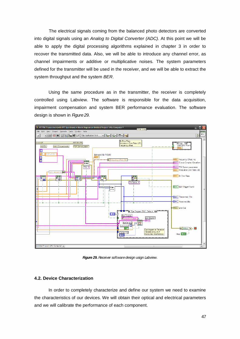
Using the same procedure as in the transmitter, the receiver is completely
controlled using Labview. The software is responsible for the data acquisition,
impairment compensation and system BER performance evaluation. The software
design is shown in Figure 29.
Figure 29. Receiver software design usign Labview.
4.2. Device Characterization
In order to completely characterize and define our system we need to examine
the characteristics of our devices. We will obtain their optical and electrical parameters
and we will calibrate the performance of each component.
48
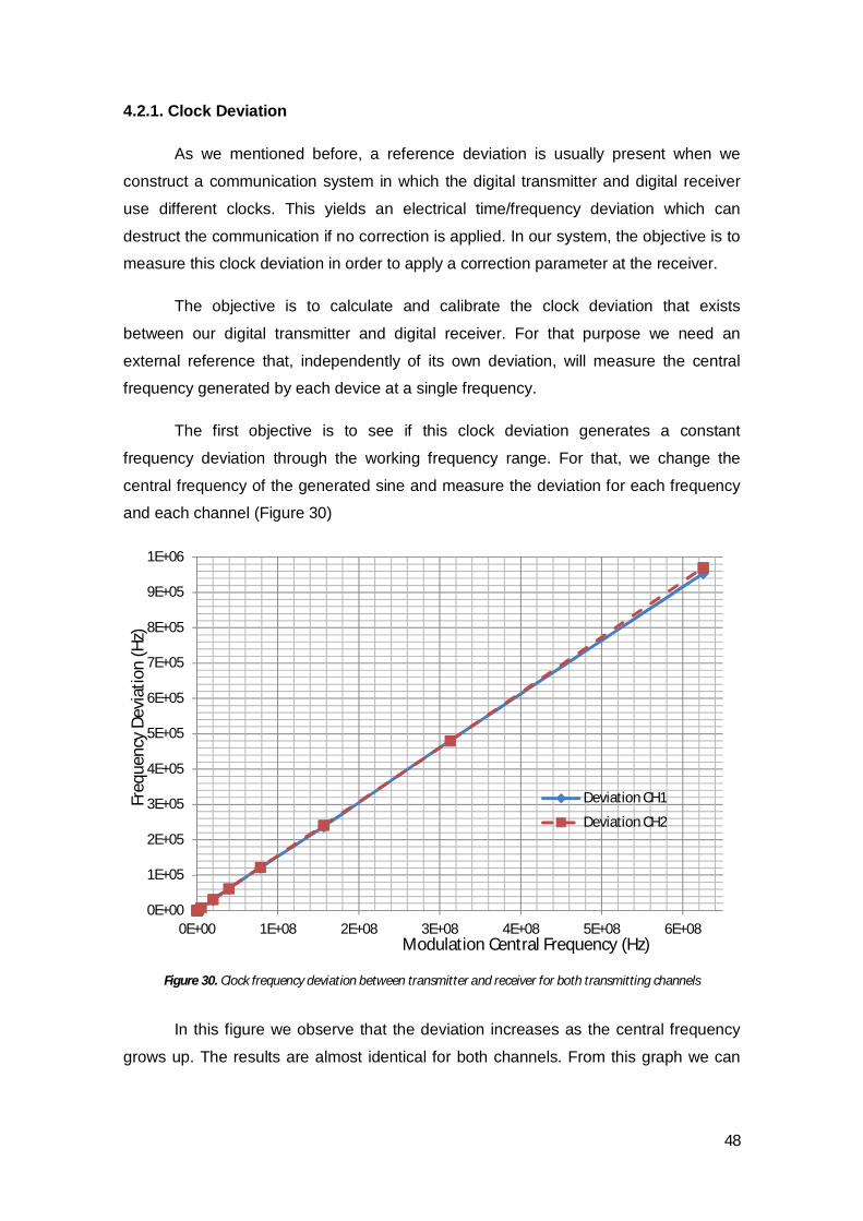
4.2.1. Clock Deviation
As we mentioned before, a reference deviation is usually present when we
construct a communication system in which the digital transmitter and digital receiver
use different clocks. This yields an electrical time/frequency deviation which can
destruct the communication if no correction is applied. In our system, the objective is to
measure this clock deviation in order to apply a correction parameter at the receiver.
The objective is to calculate and calibrate the clock deviation that exists
between our digital transmitter and digital receiver. For that purpose we need an
external reference that, independently of its own deviation, will measure the central
frequency generated by each device at a single frequency.
The first objective is to see if this clock deviation generates a constant
frequency deviation through the working frequency range. For that, we change the
central frequency of the generated sine and measure the deviation for each frequency
and each channel (Figure 30)
Figure 30. Clock frequency deviation between transmitter and receiver for both transmitting channels
In this figure we observe that the deviation increases as the central frequency
grows up. The results are almost identical for both channels. From this graph we can
0E+00
1E+05
2E+05
3E+05
4E+05
5E+05
6E+05
7E+05
8E+05
9E+05
1E+06
0E+00 1E+08 2E+08 3E+08 4E+08 5E+08 6E+08
Freq
uenc
y De
viat
ion
(Hz)
Modulation Central Frequency (Hz)
Deviation CH1
Deviation CH2

49
extract that the deviation is linear and depends on the working frequency. Another way
to look at it is by plotting the percentual deviation present for both channels.
From this graph we can extract that the deviation can be modeled as a percentual
deviation around 0.0015%. With this calibration we will be able to adjust the clock of
both systems in order to compensate this effect.
Other parameters that could influence this deviation were studied, as output
power, pre-distortion filters or output filters, but no dependences were found.
Figure 31. Relative clock frequency deviation between transmitter and receiver for both transmitting channels
4.2.2. Isolator – Thorlabs: IO-H-1550-APC
This device, which allows the transmission of light in only one direction, is
placed at the output of the laser in order to prevent the entry of any light beam into it,
which could damage our source.
Figure 32. Isolator diagram. Transmission of light is only in one direction, from port 1 to port 2.
0.0013
0.0014
0.0014
0.0015
0.0015
0.0016
0.0016
0.0017
0.0017
0E+00 1E+08 2E+08 3E+08 4E+08 5E+08 6E+08
Freq
uenc
y Dev
iatio
n (%
)
Central Frequency (Hz)
Deviation CH1Deviation CH2

50
The key characteristics of this device are obtained using a power source and a power
meter while changing the input and output.
Insertion Loss (dB) Return Loss (dB) Isolation (dB)
0.81 55.32 36.4 Table 1. Isolator characteristics
4.2.3. Circulator – Thorlabs: 6015-3-APC
This is a three-port device designed such that light entering any port exits from
the next. Circulators can be used to achieve bi-directional transmission over a single
fiber. In our system it is used to monitory the back reflections and control any possible
failure on the set-up.
Figure 33. Optical circulator scheme
The measured characteristics are:
Direction Insertion Loss (dB) Return Loss (dB) Isolation (dB)
1 -> 2 1.21 53.6
2 -> 3 1.36 53.76
2 -> 1 53.76 49.61
3 -> 2 53.24 54.703 Table 2. Circulator characteristics
4.2.4. Polarization controller – FPC030
This device allows us to modify the polarization state of the incoming light from
the laser. In our system, the modulator works only with one polarization, so we have to
adjust the polarization state at their entry on order to maximize the modulated power. In
this case it is a three freedom degree, manually controlled polarizator.

51
Direction Insertion Loss (dB) Return Loss (dB)
Input -> Output 0.293 49.76
Output -> Input 0.502 51.707 Table 3.Polarizator Controller characteristics
4.2.5 Mach Zenhder Modulator – Covega 056-003
This device is used to modulate the optical intensity by using optical
interferometry. The incoming light is divided in two beams. One of these branches is
delayed by the radiofrequency signal coming from the AWG. At the output, these two
beams are mixed, generating a constructive or destructive wave. This way we are able
to obtain an intensity modulated signal. The main characteristic of the device is the
output power as a function of the applied voltage. The results are presented on figure
34.
Figure 34. Transmission function of MZ modulator Covega 056
-20
-15
-10
-5
0
5
10
-10 -8 -6 -4 -2 0 2 4 6 8
Out
put P
ower
(dBm
)
Input Voltage (V)

52
By default, this device has been “bias trimmed” such that it’s zero-volt operating
point is near negative-slope quadrature. The implication of operating on the negative
slope quadrature point is that the modulator will cause data inversion. It can also be
corrected by applying a bias voltage to achieve operation on the positive slope
quadrature point. This is not a preferred solution as the required bias voltage will be
quite large. In our system we have the advantage that the phase offset will be
corrected by software. This means that an inversion of the data will not affect our
system and that we are able to work at the optimal bias voltage. Another important data
extracted from Figure 34. is that the maximum input voltage is ±2 V. If not, we would
introduce modulation errors and undesired effects.
Figure 35. Single port Mach Zenhder modulator model.
The chirp parameter is a key characteristic of any optical modulator. In our case
the device is zero-chirp designed, so we can neglect its effects. Other parameters are
shown in table 4.
Insertion Loss (dB) Return Loss(dB) E/O Bandwidth (GHz)
4.0 40 10.2 (data sheet) Table 4. MZ modulator Covega 056 characteristics
4.2.6. Optical attenuator – Thorlabs: CWD-AL-10H
An optical attenuator is a device used to reduce the power level of an optical
signal. In our system we use it as a local oscillator power controller.
1 2
Figure 36. Optical attenuator diagram

53
This way we can modify several parameters as the working regime or the SNR.
Insertion Loss (dB) Return Loss (dB) Maximum attenuation (dB)
1.18 55.32 160 (data sheet) Table 5. Attenuator characteristics
4.2.7. Phase shifter – Phoenix photonics VPS 15
The phase shifter is a compact, simple to operate, all-fiber device for wideband
operation. Applying a voltage to the pins it gives a controlled modification of the phase
shift through the device. The phase shifter provides phase shifts up to 50π over a
broad wavelength range.
Figure 37. Phoenix photonics phase shifter
The main characteristic we are interested in is the frequency response, shown in
Figure 38. We will use it to change the phase of the local oscillator signal in order to
prevent the power variations at the mixer output, which are due to the variation of the
laser central frequency and the path difference.
Figure 38. Phase shifter frequency response
-25
-20
-15
-10
-5
0
5
0 5 10 15 20 25 30 35
Mag
nitu
de R
espo
nse
(dB)
Frequency (KHz)

54
Also, the input voltage needed to perform a phase shift of π is calculated to be
0.05V. Other important parameters are shown in table 6.
Insertion Loss (dB) Return Loss(dB) E/O Bandwidth (KHz)
3.2 47 18.25 Table 6. Phase shifter characteristics
4.2.8. Balanced photo detector – U2T - BPDV2020R
The balanced photo detection has been widely covered on chapter 2 and its
importance has been demonstrated. In table 7 the characterization of our detector is
shown.
Return Loss (dB)
CMRR (dB) E/O Bandwidth (GHz) DC Responsivity (A/W)
24.7 15 40 (data sheet) 0.51 Table 7. Balanced photo detector characteristics
4.3. Implementation limitations and impairment effects
The main problems that exist in coherent communications have been explained
theoretically in chapter 3, but in a real system we have to take in account a greater
number of non-idealities that can influence in different manners to the obtained results.
In order to address these effects, in this chapter we will try to define this impairments,
how they influence our system, and the means to minimize its consequences.
4.3.1. Bandwidth and transmitter limitations
Considering that every device has a well-defined frequency range, where it can
work properly, we would have to define the maximum bandwidth that we can use
assuming a correct frequency response. In our case, as we can see in Table 8, the
most limited device is the arbitrary waveform generator. This means that the maximum
bandwidth that we can use to transmit data is 625MHz.
Device 3dB Bandwidth
Arbitrary Waveform Generator N82341A 625 MHz
Mach-Zehnder Covega 056 10GHz
Mach-Zehnder Covega 060 10 GHz
Balanced Photodetector BPVD-2020R 40 GHz

55
RF Amplifier ZFL-1200 1 GHz Table 8. System device bandwidths
The arbitrary waveform generator presents several parameters providing
different advantages or disadvantages with regards to the working and filtering regime
at its output. There are three key tools that control our signal generator.
The first tool is an integrated pre-distortion filter, which compensates for the
variation in the magnitude response of the output response as a function of frequency.
This process creates a linear phase response and attenuates the lower frequency
signals. The consequence is both a small dynamic range and a reduced output voltage
at all frequencies.
Another integrated tool is the reconstruction filter at 500MHz realized as a 7-pole
elliptical filter plus thru-line output. The filter purpose is to attenuate the harmonics
generated by the DAC and reduce the noise floor. In the other hand, they cause a
power loss around 2 dB and reduces the bandwidth to 500MHz.
The last parameter we can configure in the signal generator is the amplification
level. It consists on an analog amplifier, placed after the DAC, which amplifies the RF
signal. Unfortunately, it diminishes the signal purity and increase the noise floor.
In order to decide which parameters would provide us a better solution, we
present the AWG results in the table 9. Here we can see that the best noise floor level
and an acceptable harmonic generation are obtained with the pre-distortion filter active.
In this scenario, introducing the reconstruction filter doesn’t improve the performance of
the noise floor, but it would mean a high power loss.
Predist. Filter
Amplification Reconstr. Filter
Max. Power(dBm)
Noise Floor (dB)
2ndHarmonic (dB)
x x 0 -82 -53
x -0.82 -80 -71
x x x -5.84 -96 -75.19
x x -6.11 -96 -75
x -7.2 -100 -77
-10.1 -100.1 -80.3 x x -11.4 -100.1 -82.2
x -16.27 -105 -87.11
Table 9. AWG performance with different configuration tools

56
4.3.2. Laser source: line width effects.
As we saw in chapter 3, there is a phase offset ∅푺[풓풂풅] that must be calculated
in order to demodulate any M-PSK signal. Since usually the line frequency width is
much smaller than the symbol rate, it is reasonable to assume that ∅푺[풓풂풅] is
constant over each symbol duration. In real systems, we have to consider how this line
width influences the bit error rate of the system. For that we use the expression
obtained in [27]:
퐵퐸푅 =1
2휋휎푒 /( )푑휑
(4. 1)
where 휎 = 2휋휏 ∗ ∆휗[푊], 휏[푠] is the coherence time, and ∆휗[퐻푧] is the laser line
width. In Figure 39 we can see the influence of the variance on the bit error of an ideal
PSK demodulator.
Figure 39. BER performace for synchronous PSK (homodyne and heterodyne) in presence of phase noise
with a variance 흈ퟐ
Our laser specifications indicate that its Lorentzian line width is less than 0.1
Khz. Also, as we see in Figure 39, if the laser variance 휎 is lower than 0.01 there is
no effect on the system BER. This means that we can calculate the maximum
coherence time so we can avoid this effect:
휏 =
휎 ,
2휋∆휗=
0.012휋 ∗ 100
= 1.59155 × 10 [푠]
(4. 2)
This time corresponds to a symbol frequency of 62.831 Khz. The maximum
bandwidth in our system is 625 MHz, which means that the phase offset can be
calculated calculated over a maximum number of symbols 푁 calculated as:

57
푁 =
퐵푊푓
=625푥10
62.831푥10≅ 10 [푠푦푚푏표푙푠]
(4. 3)
where BW is our system bandwidth [Hz] and 푓 is the symbol frequency [Hz]. This
means that using a maximum of 10 symbols we will avoid the laser phase noise
influence over the phase offset estimation.
4.3.3. Central frequency deviation and path difference fading
Another effect that is present in self-heterodyne systems is the low frequency
beat due to the combination of two effects: the variation of the central frequency of the
laser and the path difference. At the receiver, the two optical signals are mixed in the
hybrid. These two signals have travelled through different paths which may differ on the
length (Figure 40).
Source
Beam Splitter
Signal optical pathdsi
LO optical pathdLO
CoherentDetector
Es(t)
Elo(t)
Ela(t) Eo1(t)
Eo2(t)
Figure 40. Optical path difference in self-homodyne and heterodyne systems. The light beam generated at the source 푬풍풂(풕) is separated into two beams. One will act as signal beam, 푬풐ퟏ(풕) and is sent through the system travelling a distance 풅풔풊. 푬풐ퟐ(풕) is sent to the coherent detector travelling a distance 풅푳푶, where it acts as local
oscillator 푬푳푶(풕).
If we consider that the central frequency of the laser is time-varying, at the
receiver we would have a time-dependent phase factor due to the path difference:
∆∅(푡) = ∅ (푡) − ∅ (푡) = (푑 − 푑 ) ∗2휋휆(푡)
[푟푎푑]
(4. 3)
where 푑 is the signal path, 푑 is the local oscillator path, and 휆(푡) is the
instantaneous wavelength of the laser at a concrete time t. We can express this phase
offset as a sum of two terms, a constant one and a time-dependent one:
∆∅(푡) = (푑 − 푑 )2휋푐푓 + (푑 − 푑 )
2휋푐∆푓(푡) = ∅ + ∅ (푡)[푟푎푑]
(4. 4)

58
The term ∆푓(푡)[퐻푧] introduces a time-varying phase, which self-modulates the signal
at the output of the hybrid and reduces the power detected at the balanced photo
detectors, having:
퐼(푡) = 퐾 ∗ cos[푤 푡 + ∅ − ∅ ] = 퐾 ∗ cos[푤 푡 + ∅ + ∅ (푡)][퐴] (4. 5)
To clarify the effect of this varying phase we can use the standard identity:
cos(퐴 + 퐵) = sin퐴푐표푠퐵 + 푐표푠퐴푠푖푛퐵 (4. 6)
This way we obtain an expression that relates directly the output intensity and the time-
varying phase:
퐼(푡) = 퐾{cos[푤 푡 + ∅ ] cos[∅ (푡)] − sin[푤 푡 + ∅ ] sin[∅ (푡)]}[퐴] (4. 7)
This effect can result in destructive signal interference. In order to compensate
this effect, we have to introduce a new block to control the phase of the local oscillator.
For that purpose we introduce a phase shifter after the variable attenuator. A digitally
controlled voltage source applies a voltage that controls the phase shifter. The scheme
is shown in Figure 41.
Figure 41. Local Oscillator phase controller system
The algorithm that controls the voltage source is based on the second
derivative algorithm. The objective of this algorithm is to apply phase shift
∅ (푡)[푟푎푑]that compensates the time dependent term ∅ (푡)[푟푎푑] so we get:
∅ (푡) = ∅ (푡) + ∅ (푡) = 푛휋2[푟푎푑]; 푛 = 0,1,2,3 (4. 8)

59
Theoretically, if this term is well estimated we would have only one sinusoidal
term in equation 4.7, which is our objective. In order to estimate this phase term
∅ (푡)[푟푎푑] we will focus on maximize the term |퐼(푡)|[퐴] that we get in the receiver.
By maximizing the power obtained we ensure that the resulting signal is only over one
projection of the plane. The algorithm is based on minimize the second derivative of
the intensity power by applying a phase-step with the phase shifter. Depending on the
new derivative result we will apply again the same phase-step or the negative.
In order to optimize the algorithm we need to calculate two basic parameters.
The first one is the phase step introduced by our phase shifter. Here, the voltage
source imposes a lower limit due to its minimum resolution (0.001 [V]) that corresponds
to a minimum phase step of 30. The second parameter is the sampling time used to
update the phase shifter voltage. The combination of these two parameters describes
the system response. A higher phase step at a high sampling rate could be able to
correct faster changes but it would introduce a higher ripple on stationary conditions.
On the other hand, by using a low phase step we would accurately obtain a phase
correction on stationary conditions but it won’t be able to correct fast laser changes.
For that purpose we analyze and measure the effect of these two parameters
over the losses on the average received power and on the relative fading
variance휎 /푃 , where 휎 is the power variance and 푃 is the average power.
Figure 42. Fading variance and power losses in the presence of different phase steps and sampling periods. The
ripple and power losses are minimized for a phase step of 10 degrees with an update every 50 ms.
0 5 10 15 20 25 300
1
2
3
Phase step (degrees)
Pow
er L
oss
(dB
)
0 5 10 15 20 25 30-30
-20
-10
0
Phase step (degrees)
Fadi
ng v
aria
nce
(dB
)
50 ms20 ms10 ms
50 ms20 ms10 ms

60
As we see in Figure 42 the ripple and power losses are minimized for a phase
step of 10 degrees with an update every 50 ms. The power loss at this point is 0.208
dB and the fading variance is -29.8 dB. With these results we demonstrate the
functionality of the closed loop compensation technique
4.3.4. Modulation imbalance factors
When characterizing modulation measurements, it is important to note that the
phase, amplitude, and frequency of the RF signal is obtained based on the amplitude
of each I and Q vector. Thus, errors in the baseband signal translate to errors in the RF
signal. When we work in the heterodyne scenario this effect is negligible, because the
RF signal is generated digitally, which provide us a high accuracy. In the other hand,
when we work with homodyne systems, these parameters are defined by the optical
modulator at the transmitter. Actually, this factor can increase the bit error rate. In this
section we will explain how they influence the system quality and what is the error
introduced by our own modulator. In this case we will describe the effect of the two
main factors in our system: the gain imbalance factor and the quadrature skew.
Mathematically, we can describe these effects as [28]:
퐼 = 푎 ∗ 퐼 (4. 9)
푄 = 푎 ∗ sin(휑) ∗ 퐼 + 푏 ∗ cos(휑) ∗ 푄 (4. 10)
Here 휑 is the quadrature skew, 푎 is the modulation gain at the I branch and 푏 is
modulation gain in the Q branch. The gain imbalance factor is defined as:
훾 = 20log(푎푏
)[푑퐵] (4. 11)
The gain imbalance indicates the ratio of I gain to Q gain in dB. This effect is
present in many modulators due to the possible differences between the two
modulation channels. Also, it is usually caused by amplitude errors in the DAC’s or
because of inconsistencies between each of the analog mixers. This effect, even with a
few dB, can prevent proper demodulation of the signal. In order to see how it affects
our receiver we simulate this error in the transmitter. The results can be seen in Figure
43.

61
Figure 43. System BER in the presence of different gain imbalance factors
This source of error is typically observed in the optical modulator or in the local
oscillator splitter. The problem here is that the phase introduced between the I and Q
channels is not exactly 90º. Some systems specify up to 3 degrees or more of skew
[29]. For lower order modulation schemes, quadrature skew has relatively small effect
on the system throughput. However, like other sources of error, higher order
modulation schemes are significantly impaired. In the figure 4.12, we show the
performance of our system for different magnitudes of the quadrature skew.
Figure 44. System BER in presence of quadrature skew imbalance
2 3 4 5 6 7 8 9 1010
-6
10-5
10-4
10-3
10-2
10-1
100
SNR per bit
BE
R
Ideal BER1 dB Gain Imbalance2 dB Gain Imbalance4 dB Gain Imbalance
5 5.5 6 6.5 7 7.5 8 8.5 9 9.5 1010
-6
10-5
10-4
10-3
10-2
SNR per bit
Sys
tem
BE
R
Ideal BER2 degrees4 degrees8 degrees10 degrees

62
4.4.4. Effect of asymmetric hybrids
In chapter 2 we defined the demodulation schemes and their equations
considering ideal hybrids. Now we will analyze the same equations using a generic
description of the coupler considering all the non-ideal parameters. For that, we will
model the basic coupler as [30] :
퐸퐸 = √1− 휀 √휀 ∗ 푒 ∅
√휀 ∗ 푒 ∅ √1− 휀퐸퐸 푒
(4. 12)
where ∅[rad] is the phase introduced between the two branches and 휌[푟푎푑]is the
phase shift due to the coupler. Following the same procedure as in chapter 2, we have
that:
퐸 (푡) = (√1 − 휀 ∗ 퐸 + √휀 ∗ 퐸 푒 ∅)푒 (4. 13)
from there we can obtain the correspondent intensity.
퐼 (푡) = 푅 ∗ |퐸 (푡)| = 푅 퐸 (푡) ∗ 퐸∗(푡) (4. 14)
Developing the expression we find the intensity as:
퐼 (푡) = 푅(1− 휀)|퐸 | + 푅 ∗ 휀|퐸 | + 2푅(1− 휀)휀
∗ |퐸 ||퐸 |푐표푠[(푤 − 푤 )푡 + 휃 − 휃 + 휃]
(4. 15)
Applying the same procedure for 퐼 (푡)we have that:
퐼 (푡) = 푅(1− 휀)|퐸 | + 푅 ∗ 휀|퐸 | + 2푅(1− 휀)휀
∗ |퐸 ||퐸 |푐표푠[(푤 − 푤 )푡 + 휃 − 휃 − 휃]
(4. 16)
Using balanced detection and after applying a band pass filter, the resulting
intensity is obtained as:
퐼 (푡) = 퐼 (푡) − 퐼 (푡)
= 퐾{푐표푠[(푤 − 푤 )푡 + 휃 − 휃 + 휃]
− 푐표푠[(푤 −푤 )푡 + 휃 − 휃 − 휃]}
(4. 17)
where 퐾 = 2푅(1− 휀)휀 ∗ |퐸 ||퐸 |[퐴]. In the ideal case 휃 = 휋/2[푟푎푑], which
would simplify the equations. Applying the trigonometric identity cos(훼 + 훽) =
cos(훼) cos(훽) − sin(훼) sin(훽) and substituting 훼 = (푤 − 푤 )푡 + 휃 − 휃 and 훽 = 휃we
have that the resulting intensity is:
퐼 (푡) = −2 ∗ 퐾 ∗ sin[휃] ∗ 푠푖푛[(푤 − 푤 )푡 + 휃 − 휃 ] (4. 18)
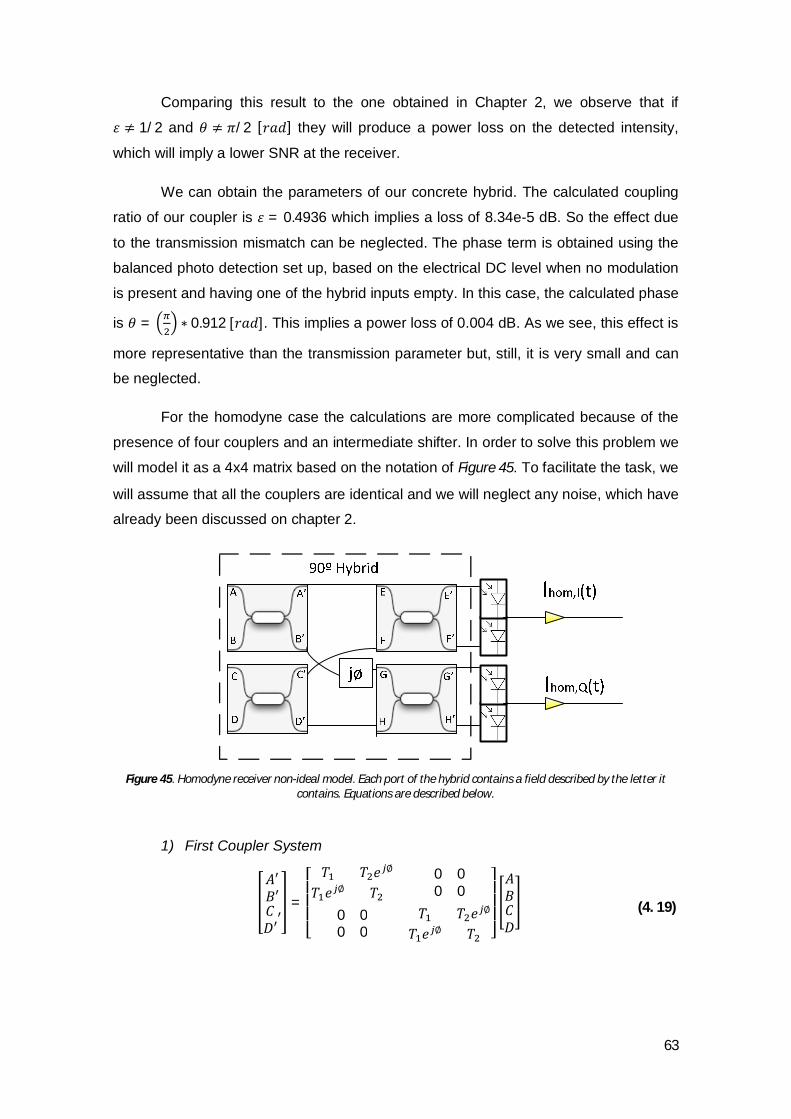
63
Comparing this result to the one obtained in Chapter 2, we observe that if
휀 ≠ 1/2 and 휃 ≠ 휋/2[푟푎푑] they will produce a power loss on the detected intensity,
which will imply a lower SNR at the receiver.
We can obtain the parameters of our concrete hybrid. The calculated coupling
ratio of our coupler is 휀 = 0.4936 which implies a loss of 8.34e-5 dB. So the effect due
to the transmission mismatch can be neglected. The phase term is obtained using the
balanced photo detection set up, based on the electrical DC level when no modulation
is present and having one of the hybrid inputs empty. In this case, the calculated phase
is 휃 = ∗ 0.912[푟푎푑]. This implies a power loss of 0.004 dB. As we see, this effect is
more representative than the transmission parameter but, still, it is very small and can
be neglected.
For the homodyne case the calculations are more complicated because of the
presence of four couplers and an intermediate shifter. In order to solve this problem we
will model it as a 4x4 matrix based on the notation of Figure 45. To facilitate the task, we
will assume that all the couplers are identical and we will neglect any noise, which have
already been discussed on chapter 2.
Figure 45. Homodyne receiver non-ideal model. Each port of the hybrid contains a field described by the letter it
contains. Equations are described below.
1) First Coupler System
퐴′퐵′퐶퐷′′
=
⎣⎢⎢⎢⎡ 푇 푇 푒 ∅
푇 푒 ∅ 푇0 00 0
0 00 0
푇 푇 푒 ∅
푇 푒 ∅ 푇 ⎦⎥⎥⎥⎤ 퐴퐵퐶퐷
(4. 19)
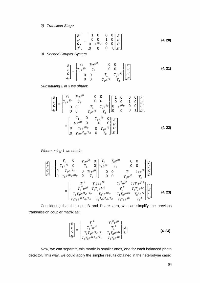
64
2) Transition Stage
퐸′퐹′퐺퐻′′
=
1 00 0
0 01 0
0 푒 ∅
0 00 00 1
퐴′퐵′퐶′퐷′
(4. 20)
3) Second Coupler System
퐸퐹퐺퐻
=
⎣⎢⎢⎢⎡ 푇 푇 푒 ∅
푇 푒 ∅ 푇0 00 0
0 00 0
푇 푇 푒 ∅
푇 푒 ∅ 푇 ⎦⎥⎥⎥⎤ 퐸′퐹′퐺′퐻′
(4. 21)
Substituting 2 in 3 we obtain:
퐸퐹퐺퐻
=
⎣⎢⎢⎢⎡ 푇 푇 푒 ∅
푇 푒 ∅ 푇0 00 0
0 00 0
푇 푇 푒 ∅
푇 푒 ∅ 푇 ⎦⎥⎥⎥⎤ 1 0
0 00 01 0
0 푒 ∅
0 00 00 1
퐴퐵퐶퐷
=
⎣⎢⎢⎢⎡
푇 0푇 푒 ∅ 0
푇 푒 ∅ 0푇 0
0 푇 푒 ∅
0 푇 푒 ∅푒 ∅0 푇 푒 ∅
0 푇 ⎦⎥⎥⎥⎤ 퐴퐵퐶퐷
(4. 22)
Where using 1 we obtain:
퐸퐹퐺퐻
=
⎣⎢⎢⎢⎡
푇 0푇 푒 ∅ 0
푇 푒 ∅ 0푇 0
0 푇 푒 ∅
0 푇 푒 ∅푒 ∅0 푇 푒 ∅
0 푇 ⎦⎥⎥⎥⎤
⎣⎢⎢⎢⎡ 푇 푇 푒 ∅
푇 푒 ∅ 푇0 00 0
0 00 0
푇 푇 푒 ∅
푇 푒 ∅ 푇 ⎦⎥⎥⎥⎤ 퐴퐵퐶퐷
=
⎣⎢⎢⎢⎡ 푇 푇 푇 푒 ∅
푇 푒 ∅ 푇 푇 푒 ∅푇 푒 ∅ 푇 푇 푒 ∅
푇 푇 푇 푒 ∅
푇 푇 푒 ∅푒 ∅ 푇 푒 ∅
푇 푇 푒 ∅푒 ∅ 푇 푒 ∅푒 ∅푇 푇 푒 ∅ 푇 푒 ∅
푇 푇 푒 ∅ 푇 ⎦⎥⎥⎥⎤ 퐴퐵퐶퐷
(4. 23)
Considering that the input B and D are zero, we can simplify the previous
transmission coupler matrix as:
퐸퐹퐺퐻
=
⎣⎢⎢⎢⎡ 푇
푇 푒 ∅푇 푒 ∅
푇푇 푇 푒 ∅푒 ∅
푇 푇 푒 ∅푒 ∅푇 푇 푒 ∅
푇 푇 푒 ∅ ⎦⎥⎥⎥⎤퐴퐶
(4. 24)
Now, we can separate this matrix in smaller ones, one for each balanced photo
detector. This way, we could apply the simpler results obtained in the heterodyne case:

65
퐸퐹 = 푇 1 푒 ∅
푒 ∅ 1퐴퐶 (4. 25)
퐺퐻 = 푇 푇 푒 ∅ 푒 ∅ 푒 ∅
푒 (∅ ∅ ) 1퐴퐶 = 푇 푇 푒 ∅ 1 푒 ∅
푒 ∅ 1퐴푒 ∅
퐶 (4. 26)
If we observe these equations we can notice that both are very similar in
concept. The expression (4. 25) is the same as eq. (4. 12). but having the entry A shifted
∅ , which ideally is 90º. Considering perfect frequency match we can derive the
expression for the output currents of the photo detectors:
퐼 (푡) = 퐼 (푡) − 퐼 (푡) = 퐾 ∗ {푐표푠[휃 − 휃 + 휃] − 푐표푠[휃 − 휃 − 휃]}
= 2퐾 sin[휃] ∗ 푠푖푛[휃 − 휃 ]
(4. 27)
퐼 (푡) = 퐼 (푡) − 퐼 (푡)
= 퐾 ∗ {푐표푠[휃 − 휃 + ∅ + 휃] − 푐표푠[휃 − 휃 + ∅ − 휃]}
= 2퐾 sin[휃] ∗ 푠푖푛[휃 − 휃 + ∅ ]
(4. 28)
where 퐾 = 2푅푇 |퐸 ||퐸 |[퐴] and 퐾 = 2푅푇 푇 |퐸 ||퐸 |[퐴] .So we have a
very similar scenario than in the heterodyne case. The influence of the transmission
coefficients for each branch is exactly the same than in the heterodyne case, so we
can assume that their influence on the power loss is negligible. To analyze the phase
term we have to separate the two branches: for the I branch, the effect is the same as
in the heterodyne case (sin[휃]factor), but in the Q branch the sum and difference of
∅ [푟푎푑] and 휃[푟푎푑] may increase the error introduced. Let’s assume that:
∅ =휋2
+ 훿; (4. 29)
Substituting in (4. 28) we have:
퐼 (푡) = 2퐾 sin[휃] ∗ 푠푖푛 휃 − 휃 +휋2
+ 훿 = 2퐾 sin[휃] 푐표푠[휃 − 휃 + 훿]
= 2퐾 sin[휃] [cos(휃 − 휃 ) cos(훿) − sin(휃 − 휃 ) sin(훿)][퐴]
(4. 30)
This parameter cannot be neglected. As we see, it affects to the orthogonality of
I and Q branches, which may cause an additional error in compare to the heterodyne
case. The phase deviation of our hybrid is 3º, which would imply a power penalty of
0.12 dB in the worst scenario.
The effect of the transmissions parameters 푇 and 푇 is demonstrated to
diminish the output intensity of each branch. Assuming the model used before, where
푇 = √1 − 휀 and 푇 = √휀, we have that the penalization on the in-phase branch is

66
0.00223 dB and the penalization on the quadrature-branch is 1.423∗ 10 dB. We
observe that the penalization increases in compare to the heterodyne case. This is due
to the fact that the signal passes through twice the couplers. Still, the penalization is
small enough to be neglected.
4.4. System parameters
In order to test the behavior of the transmitter, channel and receiver
implementation, LabView software is used. The whole transmission system is
developed using LabView, which performs the digital signal processing and controls
the surrounding equipment using standard drivers and functions.
Figure 46. Transmitter control panel using Labview. From this panel the digital transmission parameters are configured as well as the control over the arbitrary waveform generator.
The prototype is designed with the main objective of validating the transceiver of an
optical coherent system that uses complex modulation formats as well as direct

67
methods at a maximum symbol rate of 625 MHz on single polarization. All the devices
used are commercial equipment with real and non-ideal behavior.
The signal in the heterodyne case is modulated by an electrical signal which
contains data at 312.5 Msymbols/s using a carrier at 312.5 MHz. The number of
symbols sent is based on the laser line width characterization derived on section 3.4.2.,
which implies that, at this data rate, we are able to send a maximum of 5푥10 symbols
assuming a constant phase offset. For the homodyne case we can use the whole
bandwidth available, having a data rate of 625 Msymbols/s, which implies that the
maximum number of symbols while the phase offset is constant is10 . In both systems,
the data rate is chosen to be the maximum allowed by the AWG, which implies that the
transmitter will be using 2 samples per symbol in the homodyne case and 4 in the
heterodyne case. The AWG works in the optimal scenario shown in chapter 3.4.1.,
using a pre-distortion filter, maximum amplification and no filter at 500MHz.
Figure 47. Receiver control panel using Labview. From this panel we are able to control the receiver parameters, the A/D acquisition configuration and the local oscillator phase control. At the same time it implements the
demodulation process, presenting the IQ diagram and demodulated I and Q signals.

68
The shape filter used can be modified by parameterization, being able to use
raised cosine, root raised cosine, Gaussian filter or none. The fixed preamble used to
solve the phase ambiguity at the receiver is chosen to be eleven symbols and it is
configured in order to be unique. In the transmitter it is also possible to configure other
parameters as frequency deviation, white noise addition or IQ impairments.
At the receiver, a variable attenuator controls the local oscillator power that
arrives to the hybrids of 90º and 180º. In the heterodyne case a phase shifter controlled
by a low bandwidth AWG is introduced. Balanced photo detectors translate the optical
signal into electrical signals, which are sampled by a digital oscilloscope working at a
sampling rate of 4 GHz, which uses 8 and 16 samples per symbol for the homodyne
and heterodyne case. Digital filtering is applied by re-sampling and channel
impairments are optionally applied using additive and multiplicative noises. The digital
signal processing algorithms explained in chapter 2 are used applying the system
parameters defined in the transmitter.
After demodulation in burst mode the system bit error rate can be calculated
under different simulation characteristics and system parameters, which allow us a high
flexibility on the system definition.

69
Chapter 5
Chapter 5. System Validation
In this Chapter the robustness of the whole coherent system is tested. First of all, the
functionality of the receiver in absence of impairments is checked to demonstrate the system
validation. We will calculate the signal to noise ratio for the homodyne and heterodyne cases.
We will compare the throughput of the system to the ideal receiver and theoretic limit. Then,
we continue testing the behavior of our system in presence of shot noise (white Gaussian
additive noise, AWGN).
From our tests, it is demonstrated that the system is able to send and receive
information using a single polarization complex modulation, achieving different data rate as a
function of the system parameters used. We will also test the BER performance of the system
in absence of each compensation block, which will indicate the performance improvement and
penalization that introduces each block. From this study it is shown that the phase and
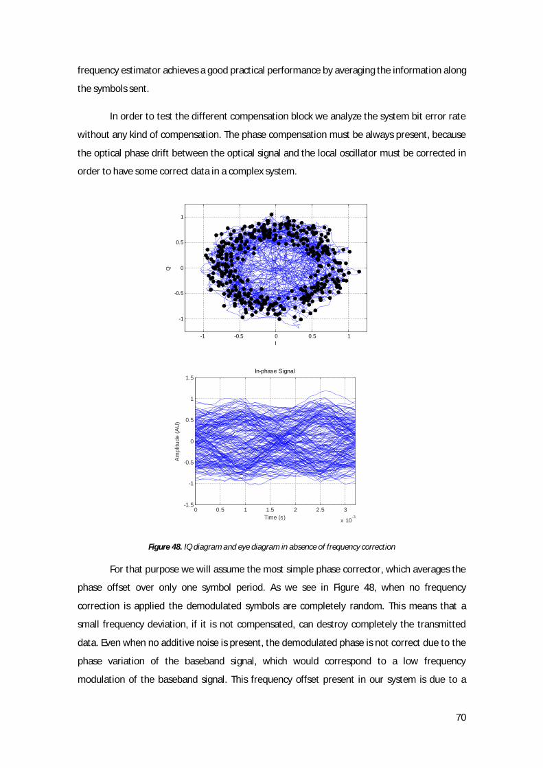
70
frequency estimator achieves a good practical performance by averaging the information along
the symbols sent.
In order to test the different compensation block we analyze the system bit error rate
without any kind of compensation. The phase compensation must be always present, because
the optical phase drift between the optical signal and the local oscillator must be corrected in
order to have some correct data in a complex system.
Figure 48. IQ diagram and eye diagram in absence of frequency correction
For that purpose we will assume the most simple phase corrector, which averages the
phase offset over only one symbol period. As we see in Figure 48, when no frequency
correction is applied the demodulated symbols are completely random. This means that a
small frequency deviation, if it is not compensated, can destroy completely the transmitted
data. Even when no additive noise is present, the demodulated phase is not correct due to the
phase variation of the baseband signal, which would correspond to a low frequency
modulation of the baseband signal. This frequency offset present in our system is due to a
-1 -0.5 0 0.5 1
-1
-0.5
0
0.5
1
I
Q
0 0.5 1 1.5 2 2.5 3
x 10-3
-1.5
-1
-0.5
0
0.5
1
1.5In-phase Signal
Time (s)
Am
plitu
de (A
U)
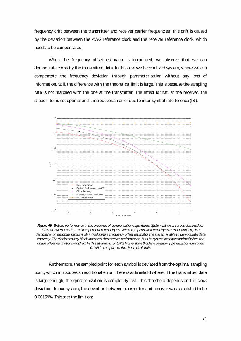
71
frequency drift between the transmitter and receiver carrier frequencies. This drift is caused
by the deviation between the AWG reference clock and the receiver reference clock, which
needs to be compensated.
When the frequency offset estimator is introduced, we observe that we can
demodulate correctly the transmitted data. In this case we have a fixed system, where we can
compensate the frequency deviation through parameterization without any loss of
information. Still, the difference with the theoretical limit is large. This is because the sampling
rate is not matched with the one at the transmitter. The effect is that, at the receiver, the
shape filter is not optimal and it introduces an error due to inter-symbol-interference (ISI).
Figure 49. System performance in the presence of compensation algorithms. System bit error rate is obtained for
different SNR scenarios and compensation techniques. When compensation techniques are not applied, data demodulation becomes random. By introducing a frequency offset estimator the system is able to demodulate data correctly. The clock recovery block improves the receiver performance, but the system becomes optimal when the phase offset estimator is applied. In this situation, for SNRs higher than 8 dB the sensitivity penalization is around
0.1dB in compare to the theoretical limit.
Furthermore, the sampled point for each symbol is deviated from the optimal sampling
point, which introduces an additional error. There is a threshold where, if the transmitted data
is large enough, the synchronization is completely lost. This threshold depends on the clock
deviation. In our system, the deviation between transmitter and receiver was calculated to be
0.00159%. This sets the limit on:
2 4 6 8 10 1210-6
10-5
10-4
10-3
10-2
10-1
100
SNR per bit (dB)
BE
R
Ideal HeterodyneSystem Performance N=500Clock RecoveryFrquency Offset CorrectionNo Compensation

72
푁 , =1
0.00159= 628[푠푦푚푏표푙푠]; (4. 31)
The BER shown in Figure 49 is calculated using 500 symbols (N) in order to avoid this
situation for the scenario without clock recovery.
When the clock recovery block is included, the behavior of the receiver improves up to
6dB, obtaining a closer curve to the theoretic results. At this point we still have a penalization
close to 1.5 dB, which can be improved by estimating the phase offset over a higher number of
symbols. In this case we use the same number of symbols that in the no-clock recovery
scenario. The resulting BER after averaging over 500 symbols almost matches the theoretical
limit when the SNR is higher than 8dB. The small deviation present at higher SNR may be
caused by some of the impairments explained in chapter 4 as asymmetric hybrids, limited
bandwidth, or by small deviations on the frequency clock parameter estimation.
Figure 50. Receiver performance in low SNR scenarios in the presence of different compensation algorithms.
Working with a SNR of 8 dB the penalty introduced by the system over the SNR is 1.02dB. In the worst scenario, when SNR per bit is 1, the maximum penalization introduced by our receiver is 2dB.
Working with a SNR of 8 dB the penalty introduced over the SNR is 1.02 dB (Figure 50).
For lower SNRs the phase estimator losses some accuracy and the differences are higher. The
maximum penalization introduced by this block is around 2dB in the worst scenario
considered. This additional error is caused by the phase unwrapping stage, which transform a
continuous phase into a circular one. This block is needed for averaging and it uses a LMS
1 2 3 4 5 6 7 810-3
10-2
10-1
100
SNR per bit (dB)
BE
R
Ideal HeterodyneSystem Performance N=500Clock RecoveryFrquency Offset CorrectionNo Compensation

73
algorithm to implement it. At low SNRs, phase jumps are not detected and contribute
significantly to the calculated average. When the SNR is good enough to avoid this jumps the
penalty introduced is less than 0.1dB (Figure 51).
Figure 51. Receiver performance in high SNR scenarios in the presence of different compensation algorithms. The system performance working with SNR per bit higher than 8 dB almost matches the theoretical limit. The maximum
penalization introduced is 0.1dB, which demonstrates the viability of the system
From this study, the functionality of the system and blocks has been validated. The considered case is the optimal one, where the frequency offset is calculated through deterministic methods instead of using statistical ones. The results demonstrate the viability of the system and the performance of the blocks
By taking a look to the IQ diagrams we can visualize the effects already mentioned. When clock recovery is not applied the sampled point are not optimally chosen so we have a high dispersion around each ideal symbol. By adding the phase recovery at this point we see that the performance improves but the phase offset is not correctly estimated. This is due to the fact that the phase offset is calculated by using the sampled points. If these points contain an error, it will be transmitted to the phase offset estimator.
When clock recovery is applied, the sampled points are chosen to be optimal and they
are more compact around the constellation point. Still, the IQ diagram is phase shifted and the
phase estimator is needed is order to avoid errors. We get the optimum scenario by applying
both algorithms. Here, the IQ diagram presents the demodulated symbols around the ideal
8 8.5 9 9.5 10 10.5 11 11.5 12 12.5 1310-6
10-5
10-4
10-3
10-2
10-1
100
SNR per bit (dB)
BE
R
Ideal HeterodyneSystem Performance N=500Clock RecoveryFrquency Offset CorrectionNo Compensation

74
constellation points (Figure 52). The distance to the ideal point is mainly due to the additive
noise and bandwidth limitations.
The same conclusions can be obtained from the eye diagrams (Figure 53). Here the eye
opening is clearly maximized by using the whole chain of algorithm already described.
Another parameter to be studied is the number of symbols used for the phase offset
estimation. As we mentioned, there is a maximum limit of 10 symbols imposed by the
coherence time of the laser. The number of symbols to be chosen must ensure that the phase
offset is constant over that time. As we saw in previous chapters, other effects may influence
this coherent time. The central frequency deviation of the laser introduces a phase variation,
which depends on the magnitude of this variation and the path difference between signal and
local oscillator. This effect reduces the maximum limit imposed by the laser line width.
Figure 52. Demodulated IQ diagram working with an SNR of 10 dB and (a) No clock recovery and no phase estimation (b) no clock recovery and phase estimation (c) clock recovery and no phase estimation (d) frequency and phase
compensation and clock recovery.
-1 -0.5 0 0.5 1
-1
-0.5
0
0.5
1
I
Q
No Clock Recovery & No Phase Estimation
-1 -0.5 0 0.5 1
-1
-0.5
0
0.5
1
I
QSystem Performance
-1 -0.5 0 0.5 1
-1
-0.5
0
0.5
1
I
Q
No Clock Recovery & Phase Estimation
-1 -0.5 0 0.5 1
-1
-0.5
0
0.5
1
I
Q
Clock Recovery & No Phase Estimation

75
We proved that the maximum frequency variations produced at the receiver are
around 1 Hz, so to ensure a constant offset the maximum coherence time must be much lower
than this quantity.
In order to measure this effect in our receiver we calculate the system BER for a
different number of symbols. The results are shown in Figure . The objective is to find an
optimal number of symbols which minimizes the penalization. In the graph we observe that by
choosing N=50 or N= 200 we introduce a penalization around 0.5dB. This is because the phase
estimator has not enough data to completely estimate the phase in the presence of noise. If
we increase N up to 500 symbols the optimum BER is obtained. When we keep increasing the
number of symbols we get a slightly higher penalization, which is approximately 0.3dB. The
reason of this penalization is that, despite the better theoretical performance in presence of
noise, we reach the phase coherence time.
Figure 53. Eye diagram at the receiver using (a) No clock recovery and no phase estimation (b) no clock recovery and phase estimation (c) clock recovery and no phase estimation (d)
frequency and phase compensation and clock recovery.
0 1 2 3
x 10-3
-1
-0.5
0
0.5
1
Time (s)
Am
plitu
de (A
U)
0 1 2 3
x 10-3
-1
-0.5
0
0.5
1
Time (s)A
mpl
itude
(AU
)
0 1 2 3
x 10-3
-1
-0.5
0
0.5
1
Time (s)
Am
plitu
de (A
U)
0 1 2 3
x 10-3
-1
-0.5
0
0.5
1
Time (s)
Am
plitu
de (A
U)
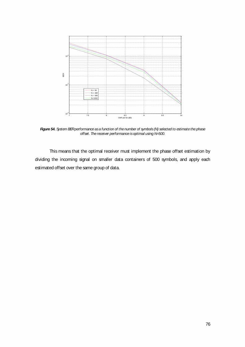
76
Figure 54. System BER performance as a function of the number of symbols (N) selected to estimate the phase
offset. The receiver performance is optimal using N=500.
This means that the optimal receiver must implement the phase offset estimation by
dividing the incoming signal on smaller data containers of 500 symbols, and apply each
estimated offset over the same group of data.
7 7.5 8 8.5 9 9.5 1010-4
10-3
10-2
SNR per bit (dB)
BE
R
N = 50N = 200N = 500N=1000

77
Chapter 6
6. Conclusions and future work
In this work a study and implementation of an optical coherent transmission system
has been made and demonstrated. The theory and basics of this technology are presented, as
well as the digital system processing needed to obtain a robust communication system.
Afterwards, a practical system has been designed, implemented and tested. The coherent
system implementation has shown the viability of optical communications using complex
modulation formats, which improves the spectral efficiency and provides better sensitivity at
the receiver.
The following objectives and conclusions have been accomplished in this project:
An optical coherent communication system has been designed and implemented.
Its robustness has been demonstrated by reaching the theoretical performance
limit in the presence of AWGN for SNR higher than 10 dB.

78
For SNRs lower than 10 dB we cannot model the system as ideal, but still the
system performance is 1.5 dB from the theoretical limit.
Digital signal processing has been proved to be advantageous and essential in a real
optical coherent receiver. A frequency offset estimation algorithm is mandatory in any
system. Also, phase estimation and clock recovery strongly improve the receiver
performance.
The implementation limits have been studied. The performance penalization
introduced by the parameters of physical devices has been studied and quantified.
A feed-back control system was implemented in order to compensate the power
fading due to destructive interferometry at the receiver.
With coherent communications we are able to introduce information in the phase,
frequency and amplitude signal by using the front-end architectures described in this project.
Balanced photo detection is today a must in coherent detection due to two main reasons: it
provides twice the power than non-balanced detection and minimizes the effect of the noise
present in the photodiodes. Once the received signal is translated to the digital domain we are
able to implement real-time algorithms that are able to compensate the main impairments
that affect optical communications. This work is focused on the receiver design and also on the
system requirements that a prototype must have in order to provide a good practical
performance.
In this project we have shown the different coherent systems that are present
nowadays considering the advantages and disadvantages of each detection system as well as
the different sensitivities needed for each modulation format. Complex modulation formats
have been chosen due to their high spectral efficiency, their low sensitivity and the capacity of
build a practical system based on commercial devices that exist in the present.
The algorithms needed in any coherent system have been presented, studied and
implemented. Our system is based on three compensation techniques specially implemented
for coherent systems. First, a clock recovery algorithm has been designed and implemented.
Due to the fact that other existing algorithms based on statistical methods impose a
penalization on the system BER, we have decided to apply a more robust compensation. By
taking advantage of our system parameters and calibration, we are able to compensate the
clock deviation, assuming negligible the penalization introduced. Phase and frequency
estimation are implemented by using a multiply-filter-divide method, which eliminates the

79
modulation factor on phase-shift-keying communications and allow us to use statistical
algorithms to estimate these factors.
An experimental set-up has been implemented using commercial devices. We have
accomplished a detailed device characterization in order to study any possible influence of
these devices on the system. Some of these devices present some limitations that generate
differences from the ideal scenario. The penalization introduced by each one of these limiting
devices has been calculated or compensated. The bandwidth limitations impose us a
transmission upper limit of data rate. The laser source deviation introduces a maximum
coherence time that limits the number of symbols that can be used for the frequency and
phase estimation. The penalization associated to this deviation was found to be under 0.001
dB, so it can be neglected.
We have shown how the modulation imbalance factors may affect the
communications and the receiver performance. Using this theoretical approach we have been
able to calculate the penalization introduced by our modulator. For the heterodyne case, this
modulation imbalance factors can be digitally controlled and minimized, which allow us to
consider a penalization close to zero. In the homodyne case these factors could be electrically
compensated at the modulator by introducing an offset voltage or by modifying the
transmitted signal at the digital transmitter.
Also the effect and penalization of asymmetric hybrids have been studied in detail. We
have obtained the equations that show their behavior and the penalization introduced. In the
heterodyne case, the penalization introduced by our modulator is very small: 8.34e-5 dB due
to the transmission factor and 0.004 dB due to the phase deviation. In the homodyne case, our
modulator would introduce a penalization of 0.2 dB, which cannot be neglected.
We have demonstrated the system and receiver implementation viability. Our system
is able to compensate the most influential effects that appear in practical systems. It is shown
that the phase estimator achieves an excellent performance by averaging the estimation along
enough number of symbols(N). The optimal N is calculated to be around 500 samples. In this
scenario and under good SNR conditions, higher than 10 dB, we are able to maintain a system
BER very close to the theoretical limit.

80
Under these conditions our system only adds a penalization of 0.01 dB, which demonstrate the
full functionality of our prototype. Under low SNR conditions, below 8 dB, our phase estimator
introduces higher penalization due to the phase noise and phase jumps that cannot be
compensated. Still, the maximum penalization in the worst possible scenario (1dB of SNR) is
only 2.5 dB.
Figure 51. System BER on presence of AWGN. System bit error rate is obtained for different SNR scenarios and compensation techniques. When compensation techniques are not applied, data demodulation becomes random. By
introducing a frequency offset estimator the system is able to demodulate data correctly but introducing many errors. The clock recovery block improves the receiver performance, but the system becomes optimal when the
phase offset estimator is applied. In this situation, for SNRs higher than 8 dB the sensitivity penalization is around 0.1dB in compare to the theoretical limit.
This project is part of a research that, based on the implemented prototype, will study
the viability of optical coherent technology in free-space communications using compensation
techniques. The objective is to increase the flexibility of the transceiver by adding different
modulation formats as well as new optical techniques that will try to compensate the effects
introduced by the atmosphere. The results presented on this project will be the base of further
studies about the coherent receiver performance on free space communications.
2 4 6 8 10 12 1410-7
10-6
10-5
10-4
10-3
10-2
10-1
100
Eb/N0 (dB)
BE
R
Ideal HeterodyneSystem Performance N=500Clock RecoveryFrquency Offset CorrectionNo Compensation

81
Bibliography
[ 1 ] E.E. Basch and T.G. Brown, “Introduction to coherent optical fiber transmission”, IEEE Commun. Mag., vol. 23, pp. 23-30, May 1985.
[ 2 ] K.-P. Ho and J. M. Kahn, “Ultimate spectral efficiency limits in DWDM systems”, in OFC, Anaheim, CA, 2002, Paper 12B22-1.
[ 3 ] I. Lyubomirsky, C.-C. Chien, "Optical duobinary spectral efficiency versus transmission performance: Is there a tradeoff? ," Conf. Lasers . 18, 598-600 (2006).
[ 4 ] L. Kazovsky, Benedetto, S., y Willner, A. (1996). Optical fiber Communication Systems. Artech House, Norwood, primera edition. 690 pp.
[ 5 ] I. Lyuborminsky, Coherent Detection for Optical Duobinary Communications Systems. IEEE, 18(7): 868–870. (2006).
[ 6 ] Taylor, M. (2004). Coherent Detection Method Using DSP for Demodulation of Signal and Subsequent Equalization of Propagation Impairments. IEEE Photonics Technology Letters, 16(2): 674–676.
[ 7 ]Tsukamoto, S. Coherent Detection of Optical Quadrature Phase-Shift Keying Signals with Carrier Phase Estimation. Journal of Lightwave Technology, 24(1): 12–21. (2006).
[ 8 ]Ramirez Iniguez, R., Idrus, S. M., y Sun, Z. Optical Wireless Communications, IR for Wireless Connectivity. Taylor and Francis, New York, second edition. 344 pp (2008).
[ 9 ]Agrawal, G. P. Fiber-Optic Communication Systems. John Wiley and Sons, New York, third edition. 546 pp. (2002).
[ 10 ] Marsland, R. ABalanced Photoreceivers Challenge Shot-Noise Limit. Suplement to Laser Focus World, Detector Handbook. . (1994).
[ 11 ] Abbas, G. L., S., C. V.W., y Yee, T. K. Local-oscillator Excess Noise Suppresion for Homodyne and Heterodyne Detection. Optics Letters, 8(8): 419–421. (1983).
[ 12 ] Ebskamp, F. y Pedersen, R. The Application of a balanced 6-15 GHz low noise Tuned Optical Front end in a 5 Gbits/s CPFSK Heterodyne System. 18th European Conference on Optical Communication, Berlin 23-27 May, 1(1): 1375–1378. (1992).
[ 13 ] Okoshi, T. y Kikuchi, K. Coherent Optical Fiber Communications. KTK Scientific Publishers, Norwell, first edition. 261 pp. (1988).
[ 14 ] Garret, I., Bond, J., J., W., D., L., y G., J. Impact of Phase Noise inWeakly Coherent Systems: a New and Accurate Approach. Journal of Lightwave Technology, 8(4): 329–337(1990).
[ 15 ] Salz, J. Modulation and detection for coherent lightwave communication systems, IEEE Comun. Mag., vol 24, pp.38-49. (1986).
[ 16 ] Barry R.J., Lee E.A. Performance of Coherent Optical Receivers. Proceedings of the IEEE, vol. 78, no. 8, pp. 1369-1394, August 1990.

82
[ 17 ] J. R. Barry and J.M. Kahn, “Carrier synchronization for homodyne and heterodyne detection of optical quadriphase-shift keying,” J. Lightwave Technol. 10, 1939–1951 (1992).
[ 18 ] Bar-David I., Saltz J., On dual Optical detection: Homodyne and reansmitted-reference heterodyne reception. IEEE Trans. Commun, vol 36, pp.1309-1315, Dec. 1988.
[ 19 ] A. Leven, N. Kaneda, U.-V. Koc and Y.-K. Chen, “Coherent receivers for practical optical communication systems,” in Proceedings of IEEE Conference on Optical Fiber Communications, (Institute of Electrical and Electronics Engineers, Anaheim, 2007).
[ 20 ] J. G. Proakis, Digital Communications, 4th ed. McGraw-Hill, New York, 2001.
[ 21 ] Ezra Ip, Alan Pak Tao Lau, Daniel J. F. Barros, Joseph M. Kahn. Coherent detection in optical fiber systems. Optics Express , Vol. 16, No. 2. 2008.
[ 22 ] Redd, Justin. Spectral content of NRZ test patterns. The Design Magazine of the Electronics Industry Vol. 49 No. 18 p67-72. 2004.
[ 23 ] Dany-Sebastien Ly-Gagnon, Satoshi Tsukamoto, Kazuhiro Katoh, and Kazuro Kikuchi. Coherent Detection of Optical Quadrature Phase-Shift Keying Signals With Carrier Phase Estimation. Journal of lightwave technology, vol. 24, No. 1, January 2006
[ 24 ] Andreas Leve, Noriaki Kaneda, Ut-Va Koc, Young-Kai Chen, ”Frequency Estimation in Intradyne Reception”, Optical Fiber Communication and the National Fiber Optic Engineers Conference, 25-29 March 2007, pp. 1 – 3.
[ 25 ] John Francis Canny, “Finding edges and lines in images”, June 1983.
[ 26 ] D. Ly-Gagnon, S. Tsukamoto, K. Katoh, and K. Kikuchi, “Coherent detection of Optical Quadrature Phaseshift keying signals with carrier phase estimation,” J. Lightwave Technol. 24, 12-21 (2006).
[ 27 ] G. Goldfarb and L- Guifang, “BER estimation of QPSK homodyne detection with carrier phase estimation using digital processing” Optics Express, Vol 14, No 18, 2006.
[ 28 ] R. Noé, “PLL-Free Synchronous QPSK Polarization Multiplex/Diversity Receiver Concept With Digital I&Q Baseband Processing,” IEEE Photon. Technol. Lett., Vol. 17, pp. 887-889, April 2005.
[ 29 ] R. Noé. Essentials of Modern Optical Fiber Communication. Springer, 2010.
[ 30 ] H. Meyr, M. Moeneclaey, and S. Fechtel, “Digital Communication Receiver”. New York: Wiley, ch. 8.2.2. 1998.
[ 31 ] Ling Liao, Dean Samara-Rubio, Michael Morse, Ansheng Liu, Dexter Hodge, Doron Rubin, Ulrich Keil, and Thorkild Franck, "High speed silicon Mach-Zehnder modulator," Opt. Express 13, 3129-3135, 2005.
[ 32 ] T. Waite. “A Balanced Mixer for Optical Heterodyning”. Proc IEEE, Vol 54, 1966, p.334.
[ 33 ] K. Birch and M. Downs. “An updated Edlen equation for the refractive index of air”. Metrologia, 30:155-162, 1993.

83
[ 34 ] Freitas J., “Analysis of laser source birefringence and dichronism on nonlinearity in heterodyne interferometry. Measurenents” Science and technology, 8(11): 1356-1359, 1997.
[ 35 ] N. Oldman, J. Kramar and E. Teague. “Electronic limitations in phase meters for heterodyne interferometry”. Precision Engineering, 15(3):173-179, 1993.
[ 36 ] M. Wu and R. Deslattes. “Interferometry – Analytical modeling od the periodic nonlinearity in heterodyne interferometry”. Applied Optics, 37(28):6696-6700, 1998.
[ 37 ] W. Hou and X. Zhao. “Drift of non linearity in the heterodyne interferometry”. Precision Engineering, 16(1):25-35, 1994.
[ 38 ] D. Payne, A. Barlow and J. Hansen. “Development of low and high birefringent optical fibers”. IEEE journal of quantum electronics, 18(4):477-487, 1982.

84