integrated circuits for local digital …messer/papers/ieee/may...integrated circuits for local...
TRANSCRIPT

INTEGRATED CIRCUITS FOR LOCAL DIGITAL SWITCHING
LINE INTERFACES
Paul R. Gray and David G. Messerschmitt
Technological advances make exploitation of the most advanced ideas in telecommunications systems
,economically feasible.
The technology of telephony is undeniably evolving at 1950’s [3], but was not realized until the early 1970’s [4]. the fastest rate in its history. This is due only in part to In both cases, the delay from conception to realization current conceptual advances in communication theory was due to a lack of available devices to make exploita- and technique. In fact, many of the system concepts tion sufficiently economical and reliable. currently being implemented were invented and under- In the more recent case of digital switching, the first stood to have many advantages two decades ago or application was to local switches (interconnecting sub- more, but were not commercially developed at that time scribers) in France [4], and the first application in the because they were too complicated to be realized eco- United States was to toll switches [5] (interconnecting nomically or reliably. The primary driving force behind other switches). The toll application is easier to prove-in the current rapid evolution in telecommunications is economically, since the trunk interface is relatively sim- integrated circuit technology, which has increased by ple and economical as compared to the interface to a orders of magnitude the system complexity which can be subscriber line. realized economically. As a direct result of integrated To illustrate this fact, Fig. 1 shows a simplified version circuitry, our ability to economically implement tele- of an analog telephone connection in which the long-haul communications systems is finally catching up with our toll switching is done on a four-wire basis (two directions most advanced ideas as to how they should be realized. of transmission are separated on different facilities). On
. There is no better example of the foregoing than inte- the other hand, the local switch and short subscriber line grated digital transmission and switching, which is one of are two-wire (both directions share the same wire pair) to the strongest trends in the current evolution of teleph- . save copper. Conversion from two- to four-wire is ony. The technical advantages of digital pulse-code performed by a device called a hybrid, to be discussed modulation (PCM) were understood by communications later. Replacement of this analog toll switch with a digital engineers in the 1940’s [ 11, but the first PCM system was switch simply involves A/D and D/A conversion at the not commercially available until 1962 [2]. Digital switch- switch interface in the. case of an analog transmission ing of PCM streams was in an experimental state in the trunk, and more complicated but nevertheless inexpen-
sive functions such as synchronization and framing in the
Computer Sciences, University of California, Berkeley, CA 94720. Replacement of the local switch by one which switches The authors are with the Department of Electrical Engineering and case Of a digital transmission trunk.
0163-6804/80/0500-0012 $00.75 0 1980 IEEE 12 IEEE Communications Magazine

b I I
Subscriber loop
1 Fow;ire
switch
Two-wire Four-wire
b I Two-wire Four-wire
switch switch * local < p H toll
9
^ ^ . ........... .......
Fig. 1. Typical analog telephone connection.
signals in a digital PCM format is a more radical change, as shown in Fig. 2. One reason is that a digital switch must inherently separate the two directions of trans- mission, that is, it is four-wire. Thus, the hybrid moves to the subscriber side of the local switch, and must be implemented on a per subscriber line basis. A second reason is that many interface functions, such as ringing and testing, are needed to interface a subscriber line. These involve high voltages and cannot be performed by a small number of service circuits operating through the switch network itself, as was the case with metallic cross- point analog switches.
A simplified block diagram of the transmission inter-
. . I " . . . . . . . . , _ _ . I.
face between a local digital switch and a subscriber line is shown in Fig. 3. The line interface performs the hybrid function, provides dc power to the phone, and other functions. The transmit low-pass filter prevents aliasing distortion resulting from any frequency components above 4 kHz, half the subsequent sampling rate of 8 kHz. The A/D converter then converts individual samples to the digital format used internally in the switch. On the receive side, the D/A converter generates analog sam- ples and the low-pass filter reconstructs the analog speech waveform. The A/D and D/A converters to- gether are called a codec (for coder-decoder).
Virtually none of the functions in Fig. 3 is required at
I Four-wire Toil-connect
local trunk switch switch
Four-wire toll < b H
Subscriber loop
<
Two-wire Four-wire
* b
Four-wire
switch switch
Four-wire b H toll local
9 < - - I .- .- . . . . . - . . . . . . . . . . . . . . . . . . . . . . . . - ............................. -. . I . .- -- .- i
Fig. 2. Typical digital telephone connection.
May 1980 13

. . .. .. . ..
Anti-aliasing
High Z D LPF Coder
(ND conv) s Transmit
- -
Four-wire digital signal
Two-wire Line or trunk impedance
Hybrid Balancing
A
- -
Low 2 LPF
Decoder (DIA conv)
< Receive
Reconstruction I . . .. ..
Fig. 3. Block diagram of a line interface circuit. - .. i
the subscriber-line interface to a metallic crosspoint ana- log switch, since these functions are associated with A/D conversion and four-wire to two-wire conversion. There- fore, they must be implemented very inexpensively to re- sult in an economically competitive switch. Fortunately, there are offsetting savings in the local digital switch. The switching function itself is more economically realized, and the interface to digital PCM transmission trunks and subscriber line multiplex systems are much cheaper. Because these other functions are so cheap, the total cost of the digital switch is, in fact, dominated by the cost of the functions shown in Fig. 3, together with the related functions of battery feed, protection, and ringing and test access.
Because the functions on Fig. 3 must be realized inex- pensively, and because they are replicated on every sub- scriber line' and therefore will be produced in high volume, they are a natural application for special- purpose integrated circuits. This is being pursued aggressively by the vertically integrated telephone equip- ment manufacturers, and because of the potentially vast market, by many independent semiconductor manu- facturers.
The purpose of this paper is to review the functional and interface requirements, as well as circuit and tech- nology alternatives for integrated circuit codecs, filters, and line interfaces.
CODEC REQUIREMENTS The codecs utilized in telephony employ nonuniform
quantization; that is, their step size increases as the magnitude of the signal sample increases. The so-called
'Another approach to reducing the cost of these functions, an analog crosspoint concentrator switch between subscriber lines and the digi- tal switch line interfaces, will not be discussed here.
14
/I = 255 law [6] is standard in North America and Japan; Europe uses a slightly different standard, the A-law [6]. These laws provide a wide dynamic range over which the signal-to-quantization noise ratio is approximately con- stant and a very small step size near the origin.
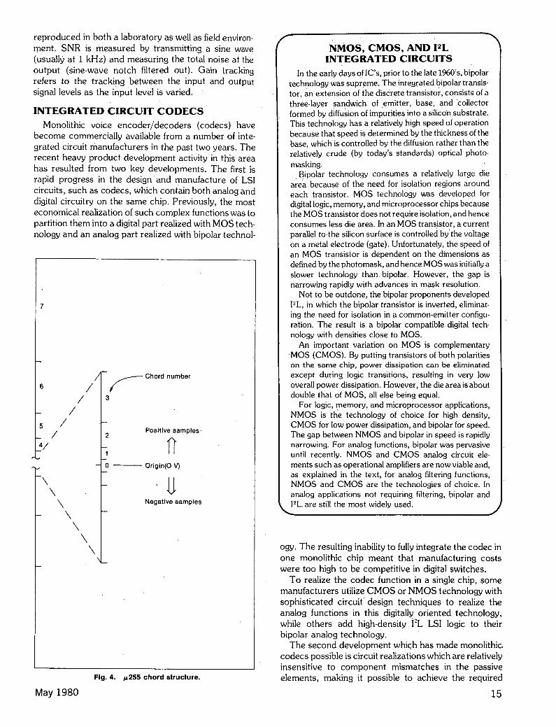
The /I = 255 coder generates an 8-bit sample, so that 256 intervals of signal level must be distinguished. The total signal range is first divided into 16 intervals (called chords), 8 for positive signals and 8 for negative. These chords double in length as they move away from the origin, as illustrated in Fig. 4. Finally, each chord is divided into 16 equal intervals to yield the 256 total intervals. There is one sign bit, three bits to specify one of eight chords, and four bits to specify the interval (out of 16) on a chord.
There are four types of requirements which are rele- vant to codec design:
1) idle channel noise 2) crosstalk coupling 3) signal-to-quantizing noise ratio (SNR) 4) gain tracking.
The first two items relate to the overall system design, rather than the coder specifically. However, relative to the design of the coder, the idle channel noise specifica- tion cannot be reliably met unless the very small step size on the lowest chord is reasonably accurate. Further, the crosstalk requirements will not be reliably achieved unless the bias of the coder for an idle channel is accurately maintained. For this reason, so-called auto zero-set circuitry is often incorporated in the codec to maintain accurate idle channel bias. It works by adjusting the bias in a feedback loop to force a positive and nega- tive sign bit with equal frequency.
The last two requirements relate to the accuracy of the A/D thresholds and D/A outputs. They are specified by simple sine-wave measurements, which are readily
IEEE Communications Magazine
reproduced in both a laboratory as well as field environ- ment. SNR is measured by transmitting a sine wave (usually at 1 kHz) and measuring the total noise at the output (sine-wave notch filtered out). Gain tracking refers to the tracking between the input and output signal levels as the input level is varied.
INTEGRATED CIRCUIT CODECS Monolithic voice encoder/decoders (codecs) have
become commercially available from a number of inte- grated circuit manufacturers in the past two years. The recent heavy product development activity in this area has resulted from two key developments. The first is rapid progress in the design ' and manufacture of LSI circuits, such as codecs, which contain both analog and digital circuitry on the same chip. Previously, the most economical realization of such complex functions was to partition them into a digital part realized with MOS tech- nology and an analog part realized with bipolar technol-
r 1
~ r Chord number 3
- n Positive samples
l? 0 - Origin(0 v) -
Negative samples -
Fig. 4. a255 chord structure. J
May 1980
NMOS, CMOS, AND 12L INTEGRATED CIRCUITS
In the early days of IC's, prior to the late 1960's, bipolar technology was supreme. The integrated bipolar transis- tor, an extension of the discrete transistor, consists of a three-layer sandwich of ,emitter, base, and 'collector formed by diffusion of impurities into a silicon substrate. This technology has a relatively high speed of operation because that speed is determined by the thickness of the base, which is controlled by the diffusion rather than the relatively crude (by today's standards) optical photo- masking.
.Bipolar technology consumes a relatively large die area because of the,need for isolation regions around each transistor. MOS technology was developed for digital logic, memory, and microprocessor chips because the MOS transistor does not require isolation, and hence consumes less die area. In an MOS transjstor, a current parallel to.the silicon surface is controlled bythe voltage on a metal electrode (gate). Unfortunately, the speed of an MOS transistor is dependent on the dimensions as defined by the photomask, and hence MOS was initially a slower technology than. bipolar. However, the gap is narrowing rapidly with advances in.mask resolution.
Not to be outdone, the bipolar proponents developed IZL, in which the bipolar transistor is inverted, eliminat- ing the need for isolation in a common-emitter configu- ration. The result is a bipolar compatible digital tech- nology with densities close to MOS.
An important variation on MOS is complementary .MOS (CMOS). By putting transistors of both polarities on the same chip, power dissipation can be eliminated except during logic transitions, resulting in very low overall power dissipation. However, the die areais about double that of MOS, all else being equal.
For logic, memory, and microprocessor applications, NMOS is the technology of choice for high density, CMOS for low power dissipation, and bipolar for speed. The gap between NMOS and bipolar in speed is rapidly narrowing. For analog functions, bipolar was pervasive until recently. NMOS and CMOS analog circuit ele- ments such as operational amplifiers are now viable and, as explained in the text, for analog filtering functions, NMOS and CMOS are the technologies of choice. In analog applications not requiring filtering, bipolar and I2L. are still the most widely used.
ogy. The resulting inability to fully integrate the codec in one monolithic chip meant that manufacturing costs were too high to be competitive in digital switches.
To realize the codec function in a single chip, some manufacturers utilize CMOS or NMOS technology with sophisticated circuit' design techniques to realize the analog functions in this digitally oriented technology, while others add high-density , 12L LSI logic to their bipolar analog technology.
The second development which has made monolithic codecs possible is circuit realizations which are relatively insensitive to component mismatches in the passive elements, making it possible to achieve the required
15

xmit > SIH Companding
DAC
A
.... xmit
4 Data clock > SAR Data buffer
xmit PCM data
< Control
< clock($ Controlltiming and
I I .1 .1 - RCV
e- Data clock RCV V Data buffer
RCV
SIH < Companding < I . . . a Data in DAC . . .
6
I ^ ^ . . . " ^ . " .
Fig. 5. Basic'WA per line codec components.
transmission performance without any trimming or other adjustment of internal components.
Beyond these common factors, the commercially available devices vary widely in their technological and circuit implementation, as well as in the peripheral features provided. In the following discussion, we survey the circuit techniques and technology used in these devices.
BASIC CODEC ARCHITECTURES Perhaps the most fundamental architectural feature of
the codec is whether one codec. is used for each subscriber line as in Fig. 3, or a high-speed coder is shared over many lines using an analog multiplexer. Shared coders result in hardware savings, but present difficult design problems in a completely monolithic realization, such as difficulty in achieving a low level of line-to-line crosstalk and in achieving the high-speed operation required. As a result, shared codecs tend to be implemented on several chips, which reduces but does not negate their potential economic advantages. A second drawback of shared coders is the larger number of lines lost upon a failure (although reasonable reliability requirements can still be met). A third drawback is that analog time-division multiplexing is more difficult and less flexible than digital multiplexing. Despite these draw- backs, shared coders will continue to receive attention in the future due to their economic advantage. 16
Most of the new product development effort in the recent past has been devoted to per-channel coders, based on the belief that a standard per-line coder can be manufactured in higher volume, resulting in a cost as low as for the shared approach. Although many algorithms have been proposed, the pervasive monolithic codec realization in the devices produced commercially is the traditional successive-approximation technique illus- trated in Fig. 5. In the encode direction, the four-wire. signal from the subscriber line, hybrid, and anti-aliasing low-pass filter (Fig..3) is sampled in the input sample/hold amplifier, and encoded using the companding DAC, voltage comparator, and successive-approximation reg- ister. The resulting data are loaded in the transmit data buffer and subsequently shifted out serially under the control of the transmit data clock. In the receive direction, the data to be decoded are shifted in serially under the control of the receive data clock, and subse- quently the decode D/A converter produces an analog voltage which is held in the output sample/hold amplifier. This signal is then connected to the reconstruction low-, pass filter (Fig. 3). In some codecs, a single DAC is time shared between the encode and decode directions (which requires complex logic in asynchronous applica- tions), and in other codecs two DAC's are used (elimi- nating this logic and the decoding sample/hold function).
The principle analog components in the codec are the D/A converter, the sample/hold amplifier, and the com-
IEEE Communications Magazine

parator: The implementation of the remaining logic cir- DAC, IMPLEMENTATION cuitry is straightforward in NMOS, CMOS, or I2L tech- In the current switching DAC, binary weighted cur- nology. The different commercially available codecs are rent sources are routed either to the output or to ground distinct primarily in the technique and technology used through current switches under the control of the digital to implement the DAC. We now discuss briefly the three input to the DAC, as shown in Fig. 6. This technique, primary approaches to the.realization of DAC’s: current which has been used for many years in uniform step-size switching, resistor string, and charge redistribution. codecs (monolithic, hybrid and discrete), is well suited to
- - -
(1 - 11/16) I, 1 i n / 1 6 I,
16-step - 4-bit current digital divider step number
Analog out
T
May 1980
Current source array
rJ - -# -!At this point
I goes directly to output
Digital in
Fig. 6. Current-switched companding DAC.
1, V-
17

bipolar technology. An important advance in the devel- opment of monolithic current-switched codecs was the development of circuit techniques in which the trans- mission properties of a nonuniform step-size codec are relatively insensitive to the mismatch in the resistors controlling the current sources. The current switched DAC is capable of high-speed operation, but also requires a relatively large silicon area. It has been imple- mented in both I*L [7] and CMOS [8] technologies.
Much of the early work on codecs was directed to- + wards realizing the DAC in MOS technology so that the
dense MOS logic could be used for the digital portions. For the implementation of analog circuits, the MOS transistor is inherently more suited to voltage and charge switching than is the bipolar transistor, has essentially infinite input impedance when used as an amplifier, and MOS technology inherently produces capacitors of very high linearity and stability. These capabilities have led to
.. .
the use of two nontraditional techniques to implement DAC’s in MOS technology: resistor string voltage switched DAC’s and capacitive charge-redistribution DAC’s.
An example of a resistor string DAC is shown in Fig. 7 [9], [ 101. In this case, the voltage at each junction of the resistor ladder is one-half that at the junction above it. Each of the resistors is divided into 16 segments, and the taps between these segments are connected to a tree of MOS transistors, through which any of the 256 taps of the string can be connected to the ouput.
A second MOS-compatible approach, the charge- redistribution codec [11]-[ 141, utilizes capacitors, rather than resistors, as precision elements. A simplified schematic diagram of a charge-redistribution coder is shown in Fig. 8. The input voltage is first stored on the top array of capacitors (hence, this type of coder has an inherent sample-and-hold capability), and by shuffling
18 Fig. 7. Resistor-string companding DAC‘s.
IEEE Communications Magazine

8-bit multiplying DAC/samp,ie-hold %c" , fi"" " * '
Comparator -
I ' 1 I 1 1 1 1 1
out
. -
Fig. 8. Charge redistribution coder.
charges'around among the capacitors using the MOS switches, the successive bits are generated in eight comparison/decision cycles.
The primary advantages of this type of coder are,the inherent sample/hold capability, the low power dissipa- tion because no current flows in the array, and good behavior through the origin. A disadvantage is that two DAC's are required for a complete codec.
FILTERS Both the transmit and receive filters are basically low-
pass filters which reject frequencies above 3 kHz. However, the transmit filter must also attenuate any 60 Hz input component (such as could be induced into the subscriber loop from nearby power lines), and thus becomes in reality a bandpass filter from 300 to 3000 Hz. As with most filters the performance specifications are in terms of passband and stopband attenuation. In this case, the passband ripple. specification is quite tight because of concern about transmission quality when a number of these filters are placed in tandem (they appear in PCM digital transmission systems as well). The stop- band attenuation requirements relate to frequencies above 4 kHz, which would alias back in-band due to sampling.
In addition to attenuation requirements, the filters will also contribute to crosstalk and idle channel noise. If more than one filter is put in a single monolithic device, care must be exercised to ensure a large crosstalk
attenuation between them and little crosstalk coupling through the power supply.
' One additional filter requirement relates to the phase response, which is important in voiceband data trans- mission. The phase response must meet certain linearity requirements, which are usually specified by PAR (peak- to-average ratio) [ 151.
MONOLITHIC FILTERS Great progress has been made in the past several
years in the area of monolithic analog filters, which as late as 1975 did not appear to be feasible. CCD (charge- coupled device) transversal filters had been under devel- opment since 1969, but since they were NMOS devices, there was no way to include the peripheral signal extrac- tion circuitry and a number of peripheral operational amplifiers, etc., were required to implement a complete filter function.
Three developments have changed this picture. First, techniques have evolved for the design of NMOS opera tional amplifiers [ 161, [ 171 and other analog functions, so that these can now be included on the CCD chip in a completely self-contained filter. Seco'nd, two new mono- lithic filtering techniques evolved, including the MOS- compatible switched capacitor filter and the bipolar- compatible frequency-locked filter [ 181. The latter appears to be significantly inferior to CCD and switched capacitor filters in terms of die area and so will not be discussed further here.
We next review the basic principles of operation of CCD and switched capacitor filters.
May 1980 19

CCD TRANSVERSAL FILTERS A CCD consists of a series of potential wells under
which charges can be moved under the control of elec- trodes on the surface of the silicon. The device can realize a transversal filter function by injecting charge packets at one end proportional to the input signal, and using surface electrodes along the channel to sense the charges and develop a weighted sum of the delayed samples of the input signal.
An important problem in CCD filters has been the fact that the output signal sensing amplifier had to sense small differences in charge output in the presence of large common-mode charges, resulting in severe re- quirements on the MOS-com'patible sensing amplifier and an inadequate dynamic range. This problem has been solved using the double-split electrode struc- ture [19] in which a large center section of the CCD electrodes is electrically grounded. This plus the devel- opment of NMOS operational amplifiers for on-chip signal extraction circuitry has made the self-contained CCD filter a viable competitor to the traditional hybrid and discrete component approaches.
r i
Fig. 9. Switched-capacitor resistor.
SWITCHED CAPACITOR FILTERS The switched capacitor filter utilizes a small capacitor
switched at a high rate to emulate the behavior of a resis- tor, and permits most classical active RC filtering tech- niques to be realized in completely monolithic form.
The basic concept of the switched capacitor "resistor" is illustrated in Fig. 9 [20], [21]. If the capacitor is first charged to voltage V1, and subsequently discharged to voltage V2, then an amount of charge equal to C ( Vl-V2) will have flowed from source V1 to source V2. If the switching operation is performed at a rate f , then the average current is simplyfC(Vl-V2). Thus, the switched capacitor behaves like a resistance l/fC. The delay inherent in the switching process must also be taken into account in the detailed design process.
The application of the concept in a simple single-time- constant circuit is illustrated-in Fig. 10. Here the continu- ous resistor is replaced by the switched capacitor resis- tor to yield a single-pole filter whose cutoff frequency depends only on a capacitor ratio and the externally supplied dock frequency rather than the RC product as in the continuous case. Capacitor ratios can be accu- rately controlled in MOS technology without trimming or other adjustments.
The transmission performance requirements on PCM filters generally dictate that they be realized with a five- pole, four-zero elliptic configuration. A doubly termi-
Fig. 10. Switched-capacitor filter elements.
nated passive LC network realization has excellent sensitivity properties and can be transformed into an active ladder equivalent [22], [23] and then to aswitched capacitor equivalent (by simply replacing the analog inte- grators with switched capacitor integrators).
Switched-capacitor filters which are commercially available [24] include both transmit and receive filters, internal clock generation, continuous anti-aliasing filters, the 50/60 Hz high-pass hum rejection filter, and a trans- former driver to interface directly with a hybrid trans- former.
LINE INTERFACES The seven primary functions which a line interface
must provide are 1) battery feed (powering the telephone) 2) line supervision (determining when the telephone is
3) ringing access 4) test access 5) overvoltage protection 6) two-wire to four-wire conversion (hybrid) 7) balanced to unbalanced transmission conversion
(for immunity to noise on the subscriber loop). Items 3) and 4) are generally provided by interrupting
the line with a relay. The battery feed circuit must pro- vide. a relatively low impedance at dc and simultaneously a high impedance at voice frequencies to avoid shorting out the signal path (traditionally done with a large series inductance). Supervision is defined as the detection of dc current flowing in the loop, indicating an off-hook tele- phone (and also used to detect dial pulses, which consist of a periodic interruption of dc continuity). Overvoltages which must be protected against include induced 60'Hz from power lines and the occasional power line cross or lightning strike (limited by external protective devices to about 1000 V).
The purpose of the hybrid can be seen in Fig. 11. The four-wire path constitutes a closed feedback path through the two hybrids on each end of a connection. The hybrid must present a high loss from the four-wire port to four-wire port, thereby preventing oscillation and the two types of echo shown, while simultaneously presenting a low loss on the talker speech path from the two-wire port to both four-wire ports. It can be imple- mented with transformer windings or with a single can- celling filter, and in both cases requires knowledge of the subscriber loop impedance to achieve balance.
off-hook)
20 IEEE Communications Magazine

One problem which has arisen in local digital switching is that when the switch desirably has no insertion loss between two-wire ports, the loss around the four-wire path is not always adequate when a single compromise balance impedance is used [25], [26]. However, studies have shown that two balance impedances, one for each of two common types of subscriber loops, would be adequate. Techniques for selecting the appropriate balance network automatically are being developed.
The final line interface requirement is the balanced-to- unbalanced conversion. Induced 60 Hz, noise, and crosstalk from the subscriber loop are common mode signals, appearing equally on both wires (in telephony, a common-mode signal is called a longitudinal signal). Thus, by inputting to the filter only the difference be- tween the voltages on the two wires (called the metallic signal), these unwanted longitudinal signals are rejected.
MONOLITHIC LINE INTERFACE CIRCUITS Considerable effort is currently underway in the semi-
conductor industry and at telephone industry labora- tories to provide a low-cost all-silicon replacement for the line interface function which is now performed with a transformer. Parallel efforts are underway to provide the
L r
Talker Listener
x
I ! I
Talker ! speech path
Talker echo path I
i !
Listener echo path
I
i ! Desired hybrid characteristics:
Ports LOSS
! A to C Low -
i B t o A Low 6 t o C High
Fig. 11. Hybrid and echo paths.
May 1980
same function at lower cost by using an LSI device in conjunction with an inexpensive transformer.
The basic functional configuration for an all-silicon approach is shown in block diagram form in Fig. 12. The transmit and receive four-wire signals to and from the filter are shown on the left, and the two leads of the sub- scriber line are shown on the right. The two other essen- tial connections are battery ground and the -48 to -56 v battery voltage. The overriding consideration is that voltage surges on the order of 1000 V can occur, but the maximum voltage difference that can be accommodated between any two leads on integrated circuits with low- cost production technologies available today is about 100 V. This means that an external series element must be placed in the subscriber line leads to provide the re- maining 900 V or so of voltage drop, and some form of diode clamp must be provided to clamp the terminals of the IC so that they do not exceed the battery voltage. Perhaps the most straightforward way of achieving this is shown in Fig. 12.
Once this basic configuration is adopted, a second problem is that normal operation must be maintained in the presence of large common-mode (longitudinal) volt- ages. One possibility would be to have the T' and R' terminals of the IC behave like a floating voltage source for common-mode signals so that no current would flow as a result of these common-mode signals. Unfortu- nately, this would cause the protection diodes to forward bias, making normal operation impossible. The only remaining option is to make the line circuit look like a short circuit to common-mode signals, so that the T'and R terminals maintain a constant dc voltage with respect to each other and with respect to ground when the common-mode signals are applied. This implies large longitudinal currents that must be absorbed in the mono- lithic circuit; resulting in substantially increased power dissipation as compared to a transformer interface.
In addition, the line interface must provide the basi- cally inductive impedance variation with frequency (low impedance at dc and high impedance at voice frequen- cies), which implies internal active circuitry. This active circuitry can take two forms: current drive with voltage sensing, and voltage drive with current sensing. In the current drive configuration, two controlled equal current sources are used to drive the line. The voltage across the line is sensed by a differential amplifier, and a control circuit is used to provide an active feedback path to give the desired relation between line voltage and line cur- rent. Since the desired ac and dc imped.ances are differ- ent, the control function contains a frequency selective filter. The advantage of this circuit is that it appears to be possible to implement it rather simply using a current mirror [27]. The basic voltage drive configuration, which requires less power dissipation in the presence of large longitudinal currents, consists of two voltage amplifiers connected as a bridge output amplifier. The loop cur- rent is sensed by two series resistors and converted to a single-ended signal. This signal is then used to make the
21

Fig. 12. Basic considerations in SLIC's.
loop voltage have the desired dependence on loop cur- rent so as to achieve the correct impedance.
The hybrid function can be realized without a trans- former by inserting a voltage divider to model the voltage divider formed by the output impedance of the line interface unit and the impedance presented by the line, and using the output of this voltage divider to cancel the unwanted feedthrough from the four-wire path to the four-wire path. Typically the required balance network is a very simple RC network, which can conveniently be realized using the switched capacitor techniques de- sc.ribed earlier.
Several manufacturers have under development fully integrated line interface circuitry which utilizes current drive with voltage sensing with either external or internal high current transistors to realize the current sources.
Perhaps the most difficult problem facing the solid- state line circuits is reliability. The devices will have to operate in an .environment where they are thermally cycled, experience high voltage, and experience large surges in current and voltage. Whether or not such devices can achieve the stringent reliability requirements under such conditions remains to be seen. In the next few years, it should become apparent whether the opti- mum solution to the problem is an all-silicon line inter- face or one which incorporates a transformer.
As can now be better appreciated, the transformer is a simple device beautifully suited to the task of providing simultaneously isolation from foreign potentials, the correct impedance levels, battery feed, and longitudinal signal rejection. Its primary problem is that, in the traditional configuration, it must carry the large dc bat- tery feed current, which requires a bulky and expensive core to avoid magnetic saturation. However, at least two methods have been investigated to essentially eliminate this dc magnetic flux, yielding a smaller and less expen- sive transformer; One method is to drive a secondary winding with a current source so as to null the dc flux. The primary current can be sensed (partially negating the isolation advantages of the transformer) or the magnetic flux can be sensed directly, as with a Hall effect device.'The disadvantage of this approach,'its additional power consumption, is overcome by the other approach, which i s to use a floating battery feed circuit on the pri-
mary side of the transformer, with a capacitor blocking the current from flowing in the transformer itself [28]. Because the circuit is at a floating potential with respect to ground, it is inherently insusceptible to longitudinal foreign potentials, and longitudinal balance is inherently very good. It can also be designed to have a lower power dissipation than traditional battery feed circuits.
CONCLUSIONS It is clear that the devices which have been described
here have already made a major impact in the telephone industry. The prime example is local digital switching, which is economical largely as a result of these devices, and is being actively pursued by every major telephone switching equipment manufacturer.
FUTURE TRENDS IN TELECOM IC's Advances in both circuit techniques and in technology
will result in the combination of the codec and filter func- tions on a single chip within the next two years, sub- stantially reducing the cost of these functions. In fact, one such combination chip has reached the production stage [19]. The first of these combination chips will almost certainly utilize NMOS technology because of the higher density achievable in the digital portions.of the circuit. Beyond this development, higher circuit density may allow the inclusion of the filtering and coding func- tions for two, four, or eight lines on one chip.
Another significant development is the heavy empha- sis in the semiconductor industry at the present time on the development of high-density silicon-gate CMOS LSI technologies for low-power microprocessors and mem- ories. The result will likely be production CMOS tech- nologies which are very dense and- can be applied to telecommunications products to narrow the gap in cost between CMOS and NMOS implementations of codecs and filters. Because of the importance of power dissipa- tion in many system applications, this development could result in a long-term shift towards CMOS for these types of products.
In the line interface area, the next few years should make it clear whether an all-solid state interface or one involving a transformer is more cost effective in PBX and/or central office applications.
For the longer term, it is clear that there are other opportunities for application of special-purpose inte- grated circuits in telephony. Two which are already looming on the horizon are digital transmission. on the subscriber loop all the way to the customer premises, and techniques for the reduction of bit rate for speech transmission, of interest in subscriber loop and long-haul applications. Digital subscriber loop transmission re- quires full-duplex 64 kbit/s data transmission on a pair of wires, and will presumably require measures fo5 com- pensating for a wide range of line characteristics auto- matically. Putting codec and filter at the subscriber instrument requires low power dissipation (suggesting CMOS) in order to be powered over the loop, but also
22 IEEE Communications Magazine

will relax their transmission performance requirements (for example, the anti-aliasing low-pass filter will prob- ably be much simpler because there is no crosstalk and reduced noise). Bit rate reduction for speech would reduce the 64 kbits/s, which is difficult on longer sub- scriber loops, and would basically be an extension of the present codec technology.
The only limitation in the use of LSI components is their availability. At present, the demand for the compo- nents is greater than their supply.
REFERENCES [ l ] B.M. Oliver, J.R. Pierce,andC.E. Shannon,“PhilosophyofPCM,”
Proc. IRE, vol. 36, p. 1324, 1948. [2] D.F. Hoth, “T1 carrier system,” Bell Lab. Rec., vol. 40, p. 358,
1962. [3] H.E. Vaughn, “Research model for time separation integrated
communications,” Bell Syst. Tech. J. , vol. 38, p. 909, July 1959. [4] J. Bourbao and J.B. Jacob, “New development in E-10 digital
switching systems,” in Int. Switching Symp. Rec., 1976, p. 421. [5] H.E. Vaughn, “An introduction to No. 4 ESS,” in Int. Switching
Symp. Rec., 19,72, p. 19. [6] H. Kaneko, “A unified formulation of segment companding laws
and synthesis codecs and digital compandors,” BellSyst. Tech. J., vol. 49, p. 1555, Sept. 1970.
[7] R.A. Blauschil et al.,“A single chipI2LPCM codec,”/€EEJ. Solid- State Circuits, vol. SC-14, Feb. 1979.
[8] S. Kelley and D. Ulmer, “A single-chip CMOS PCM codec,”IEEE J . Solid-State Circuits, vol. SC-14, Feb. 1979.
[9] A.J. Cecil et a/., “A two-chip PCM codec for pecchannel appli- , cations,” in Dig. Tech. Papers, 1979 Int. Solid-State Circuits
[lo] M.E. Hoff, J . Huggins, and B.M. Warren, “An NMOS telephone ’ codec for transmission and switching applications.”lEE€J. Solid-
Conf., San Francisco, CA, Feb. 1979.
State Circuits, vol. SC-24, Feb. 1979. Y.P. Tsividis, P.R. Gray, D.A. Hodges, and J . Chacko,.‘‘A seg- mented p-255 law PCM voice encoder using NMOS technology,” IEEE 4. Solid-state Circuits, vol. SC-10, Dec. 1975. G.F. Landsburgh and G.F. Smarandious, “A two-chip PCM codec,” in Dig. Tech. Papers, 1978Int. Solid-state Circuits Conf., Feb. 1978. J.T. Daves et a/ . , “A PCM voice codec with on-chip filters,” EEE J . Solid-State Circuits, vol. SC-14, Feb. 1979. K.B. Ohri and M.J. Callahan, “Integrated PCM codec,” IEEE J. Solid-State Circuits, vol. SC-14, Feb. 1979. L.W. Campbell, “The PAR meter: Characteristics of a new voice- band rating system,” IEEE Trans. Commun. Techno!., vol. COM- 18, p. 147;Apr. 1970. Y.P. Tsividis and P.R. Grav. “An intesrated NMOS ooerational _ ,
amplifier with internal compensation,;’ IEEE J . Solid-State Cir- cuits, vol. SC-11. Dec. 1976. D. Senderowics, D.A. Hodges, and P.R. Gray, “High-perfor- mance NMOS operational amplifier,” IEEE J . Solid-state Cir- cuits, vol. SC-13, Dec. 1978. K:S. Tan and P.R. Gray, “Fully integrated analog filters using bipolar JFET technology,” !€E€ J . Solid-state Circuits, vol. SC-13, Dec. 1978. A.A. Inrahim. G.J. Huoe. andT.G. Foxall.“Double solit electrode
-. .
. , transversal filter for te~ecommunicationS appIicatiAs,” IEEE J. Solid-state Circuits, vol. SC-14, Feb: 1979. B.J. Hostica, R.W. Brodersen, and P.R. Gray, “MOS sampled data recursive filters using state switched capacitor integrators,” \E€€ J . Solid-state Circuits, vol. SC-12, Dec. 1977. J.T. Caves, M. C,opeland, C.F. Rahim, and S.D. Rosenbaum, “Sampled data analog filtering using switched capacitors as re- sistors equivalents,” IEEE J. Solid-State Circuits, vol. SC-12, Dec. 1977. D.J. Allstott, R.W. Brodersen, and P.R. Gray, “MOS switched capacitor ladder filters,” IEEE J. Solid-State Circuits, vol. SC-14, Dec. 1978. G.M. Jacobs, D.J. AIIStott, R.W. Brodersen, and P.R. Gray, “Design techniques for MOS switched capacitor ladder filters,” I€EE Trans. Circuits Syst., Dec. 1978.
May 1980
P.R. Gray, D. Senderowics, H. Ohara, and B.W. Warren, “A single chip NMOS dual channel filter for PCM telephony applica- tions,” in Dig. Tech. Papers, 1979Int. Solid-State Circuits Conf., Feb. 1979. L.S. DiBiaso, “Transmission considerations for the local switched digital network,” Telephony, p. 40, Oct. 23, 1977. R.L. Bunker, F.J. Scida, and R.P. McCabe, “Line matching net- works to support zero-loss operation in digital class 5 offices,” presented at the Int. Conf. on Subscriber Loops and Syst., Atlanta, GA, Mar. 1978. F. Boxall, “Hybrid circuit,” U S . Patent 4 004 109, Jan. 18, 1977. H.E. Mussman and D.F. Smith, “Design techniques which reduce the size and power of the subscriber interface to a local exchange,” in Conf. Rec., 1978 Zurich Seminar on Digital Commun
Paul R. Gray was born in Jonesboro, AR, on December 8, 1942. He received the B.S., MS., and Ph.D. degrees in 1963, 1965, and 1969, respectively, from the University of Arizona, Tucson.
From 1969 to 1971 he was a member of the Technical Staff at Fairchild Research and Development Laboratories, where he was involved in the development of new circuit techniques and technologies for use in analog integrated circuits. In 1971 he became a Visit-
ing Lecturer in the Department of Electrical Engineering and Com- puter Sciences, University of California, Berkeley, where he is now a Professor. His research activity at Berkeley has involved new circuit techniques and computer design aids for MOS and bipolar integrated circuits, and he has coauthored a book on the subject.
Dr. Gray has served as Consultant to a number of semiconductor manufacturers. During the academic year 1977-1978 he took a leave of absence from Berkeley to serve as Project Manager for PCM filter development with Intel Corporation. Dr. Gray is a member of Eta Kappa Nu and Sigma Xi, and served as Editor of the IEEE JOURNAL OF SOLID-STATE CIRCUITS from 1977 through 1979.
23