inelastic effects in low-energy electron reflectivity of
TRANSCRIPT

Inelastic effects in low-energy electron reflectivity of two-dimensional materialsQin Gao, Patrick C. Mende, Michael Widom, and Randall M. Feenstra Citation: Journal of Vacuum Science & Technology B 33, 02B105 (2015); doi: 10.1116/1.4903361 View online: http://dx.doi.org/10.1116/1.4903361 View Table of Contents: http://scitation.aip.org/content/avs/journal/jvstb/33/2?ver=pdfcov Published by the AVS: Science & Technology of Materials, Interfaces, and Processing Articles you may be interested in Role of multilayer-like interference effects on the transient optical response of Si3N4 films pumped with free-electron laser pulses Appl. Phys. Lett. 104, 191104 (2014); 10.1063/1.4875906 Field-effect control of tunneling barrier height by exploiting graphene's low density of states J. Appl. Phys. 113, 136502 (2013); 10.1063/1.4795542 An effective structure prediction method for layered materials based on 2D particle swarm optimization algorithm J. Chem. Phys. 137, 224108 (2012); 10.1063/1.4769731 Atomic structure of interface between monolayer Pd film and Ni(111) determined by low-energy electrondiffraction and scanning tunneling microscopy J. Appl. Phys. 108, 103521 (2010); 10.1063/1.3514156 Thickness monitoring of graphene on SiC using low-energy electron diffraction J. Vac. Sci. Technol. A 28, 958 (2010); 10.1116/1.3301621
Redistribution subject to AVS license or copyright; see http://scitation.aip.org/termsconditions. Download to IP: 128.2.118.23 On: Fri, 05 Dec 2014 20:31:27
Inelastic effects in low-energy electron reflectivity of two-dimensionalmaterials
Qin Gao, Patrick C. Mende, Michael Widom, and Randall M. Feenstraa)
Department of Physics, Carnegie Mellon University, Pittsburgh, Pennsylvania 15213
(Received 21 August 2014; accepted 24 November 2014; published 5 December 2014)
A simple method is proposed for inclusion of inelastic effects (electron absorption) in computations
of low-energy electron reflectivity (LEER) spectra. The theoretical spectra are formulated by
matching of electron wavefunctions obtained from first-principles computations in a repeated
vacuum–slab–vacuum geometry. Inelastic effects are included by allowing these states to decay in
time in accordance with an imaginary term in the potential of the slab, and by mixing of the slab
states in accordance with the same type of distribution as occurs in a free-electron model. LEER
spectra are computed for various two-dimensional materials, including free-standing multilayer
graphene, graphene on copper substrates, and hexagonal boron nitride on cobalt substrates. VC 2014American Vacuum Society. [http://dx.doi.org/10.1116/1.4903361]
I. INTRODUCTION
For decades, low-energy electrons (0–300 eV) have been
employed as a probe of the geometric and electronic struc-
ture of surfaces. Since these electrons interact very strongly
with atoms, any electrons that are elastically scattered
from the surface necessarily originate from only the top few
surface layers, hence providing a sensitive probe of the near-
surface region. In particular, the technique of low-energy
electron diffraction (LEED) has been developed by many
workers, both experimentally and theoretically.1,2 In a con-
ventional LEED instrument, a monoenergetic electron beam
is directed toward a surface, and the pattern of diffracted
beams is recorded. Each diffracted beam can be labeled by
one (or more) reciprocal lattice vector(s), g ¼ ðgx; gyÞ. These
diffraction vectors are often denoted by two integer or frac-
tional values (p,q) such that g ¼ pb1 þ qb2, where b1 and b2
are the basis vectors of the reciprocal lattice of the projected
bulk structure.3 The intensity of the diffracted beams as a
function of incident energy, IgðEÞ, can be measured. Such
IgðEÞ curves contain valuable information on the geometric
structure of the surface, in particular, for cases when the sur-
face is reconstructed giving rise to fractional p and q values.
However, in most cases, the actual atomic positions are very
difficult to directly deduce from simple inspection of the
IgðEÞ curves, so that it is necessary to perform a detailed
comparison between experimentally measured and theoreti-
cally predicted curves in order to determine the structure.1–3
The development of a theory by which LEED IgðEÞ curves
could be computed is a problem that was intensively studied
during the 1970s and 1980s.1,2 A method for addressing the
problem was eventually developed in which multiple scatter-
ing of the incident electrons was included. This procedure
entailed first considering scattering by individual atoms, then
by a collection of atoms forming a layer, and finally by a
collection of layers to form the solid. By about 1990, the the-
oretical procedures (and computer implementation) existed,
whereby the IgðEÞ curves could be computed with a fair
degree of confidence, although the theory was not reliable for
energies< 50 eV. One reason for this inaccuracy at ener-
gies< 50 eV is that the detailed electronic structure of the
solid (e.g., formation of bands) is, in fact, largely untreated in
the theory. Since that time, two important developments in
low-energy electron research have occurred: First, the devel-
opment of the low-energy electron microscope (LEEM) has
enabled measurement of IgðEÞ curves over energies of typi-
cally 0–50 eV, particularly for the (0,0) nondiffracted beam,
I0ðEÞ.4 Such measurements were performed even prior to the
LEEM,5 but they greatly gained in popularity with the advent
of the LEEM.6–12 Second, computational methods for obtain-
ing the electronic band structure of solids have greatly
advanced (i.e., not specifically for LEED), with the eventual
establishment for public-domain computer codes such as the
Vienna ab initio simulation package (VASP),13–15 which have
large numbers of experienced users and for which the pack-
ages experience continual improvements (e.g., with new
pseudopotentials and new density functionals).
With these developments, we undertook a project two years
ago in which a theoretical description of low-energy electron
reflectivity (LEER) spectra at very low energies of 0–20 eV
was formulated, employing first-principles wavefunctions
obtained from VASP.12,16,17 Linear combinations of the VASP
pseudowavefunctions were formed, such that they matched
incoming or outgoing waves in the vacuum (or the substrate).
At the very low energies, good results for LEER spectra were
obtained for the case of multilayer graphene films, both free-
standing or on a metal substrate such as copper. However,
despite this success, several limitations in the theory remained:
(1) it did not incorporate inelastic effects (electron absorption);
(2) for a film on a substrate, only simple metals having free-
electronlike states at the relevant energies could be dealt with;
and (3) the theory for diffracted beams was not developed.
In this work, we present a model for addressing the first
of these limitations regarding electron absorption. In the
model, an imaginary component to the potential in the slab
is introduced, as in past LEED theory. Then, considering
wavepackets centered about each of the VASP wavefunctions,
a phase-shift analysis on the reflected wave is employed ina)Electronic mail: [email protected]
02B105-1 J. Vac. Sci. Technol. B 33(2), Mar/Apr 2015 2166-2746/2015/33(2)/02B105/11/$30.00 VC 2014 American Vacuum Society 02B105-1
Redistribution subject to AVS license or copyright; see http://scitation.aip.org/termsconditions. Download to IP: 128.2.118.23 On: Fri, 05 Dec 2014 20:31:27
order to evaluate the time spent in the slab by the wave-
packet. From that time, and using the imaginary component
of the potential, an attenuation factor for each of the VASP
states is obtained. Then, considering the spatial exponential
decay of the actual electron wavefunctions in the near-
surface region, a distribution of the VASP states is formed to
permit that decay (with the form of the distribution taken
from a free-electron model for the states in the slab). With
this distribution, the final values for the electron reflectivity
including absorption are evaluated by summing over the
states, weighting each term by its known attenuation factor.
It is important to note that a rigorous theoretical method
for incorporating inelastic effects in very low-energy LEER
spectra already exists, from the work of Krasovskii and co-
workers.18–20 Their methodology goes well beyond the ear-
lier LEED analysis procedures in that it addresses the
detailed band structure of the solid. It also includes electron
attenuation (dealt with, again, by using an imaginary compo-
nent of the potential) as well as electron states that decay
spatially into the material, i.e., evanescent states with imagi-
nary wavevector values. The theory of Krasovskii et al. dif-
fers from our own simulation procedure for LEER spectra in
that it more exactly incorporates these evanescent (imagi-
nary wavevector) and inelastic (imaginary potential) terms
in a complete “inverse band-structure” formulation of the
problem. Their results provide a benchmark against which
we can compare our approximate results.
We emphasize that we have not in any way incorporated
the imaginary term of the potential directly into the VASP
code. Such an approach would lead to non-Hermitian matri-
ces within VASP, which would require very significant modifi-
cation of the code to handle. Rather, our approach is purely
based on postprocessing of the VASP eigenstates. We treat
these states first by neglecting any inelastic effects and form-
ing the electron reflectivity as described in our prior
works.12,16,17 We then incorporate the imaginary part of the
potential in a two-step procedure, considering both the time-
decay of individual eigenstates as well as the mixing of
eigenstates with ones nearby in energy.
This paper is organized as follows. In Sec. II, we provide
a detailed description of the model that we use for incorpo-
rating inelastic effects. In Sec. III, we provide computational
results for multilayer graphene, both free-standing and on
copper. Absorption effects are found to be small in those
cases. We also consider the case of hexagonal boron nitride
(h-BN) on cobalt substrates, for which electron absorption
effects are found to be large (due to the band structure of the
h-BN films). In general, our computed results compare well
with published experimental LEER spectra for the various
materials, and with our computational results we are able to
provide improved understanding of those spectra. Finally,
our work is summarized in Sec. IV.
II. THEORETICAL METHODOLOGY
A. Reflectivity computations without inelastic effects
Our method for obtaining the reflectivity, I0ðEÞ normal-
ized to the incident beam current, has been previously
described.12,16,17 Briefly, we first consider a periodically
repeated vacuum–slab–vacuum system, with the slab con-
sisting typically of several graphene layers (for computing
reflectivity of free-standing multilayer graphene), or several
layers of a substrate material covered on one or both sides
by layer(s) of some overlayer material (for computing reflec-
tivity of the overlayer on the substrate). In both cases, VASP
computations are performed to obtain the eigenvalues and
eigenstates of the system, usually performing computations
for a few different widths of the vacuum layer. For the case
of free-standing graphene, linear combinations of these VASP
wavefunctions are formed such that there is only an outgoing
wave on the right-hand side of the slab. On the left-hand
side, there then exist both incoming and reflected waves, and
by taking the ratio of their respective amplitudes the reflec-
tivity is obtained. For the case of an overlayer on a substrate,
the methodology also requires a VASP computation of the
bulk band structure of the periodically repeated substrate
material. For the simple-metal substrates considered to date,
they are found to have nearly free-electron (NFE) states
located above the vacuum energy, and linear combinations
of the slab states are formed to match these NFE states prop-
agating into the substrate. Then, by examination of the inci-
dent and reflected waves on the left-hand side of the slab, the
reflectivity is deduced. Our method used in the present work
is identical to that of our previous work, except for one tech-
nical detail having to do with the manner in which we reject
states of “mixed” character (which act to couple slabs in
adjoining simulation cells) from the analysis; Appendix A
describes an improved method for dealing with such states.
B. Model for inelastic effects
We now consider the inclusion of inelastic effects in the
reflectivity computation, something that was not considered
in our prior work. Consider a wavepacket centered about
some energy E, incident on a surface. In LEER measure-
ments, we are concerned with the wavepacket that is
reflected from the surface. To include inelastic effects in the
reflectivity, we employ a model consisting of two parts. In
the first part, we perform a rigorous computation of the scat-
tering phase shift of the reflected wave, and from that we can
deduce both the travel time for the reflected wavepacket and
its dwell time in the slab. This underlying basis for this anal-
ysis is well described by Merzbacher.21 Using our previous
notation,12 we consider a simulation cell extending over
�zS � z � zS, with our slab of material in the center of this
cell. We evaluate the ratio of the reflected to incident wave-
function amplitudes at the far left-hand of the cell, z ¼ �zS.
The magnitude squared of that complex quantity gives us the
reflectivity, as described previously.12,17 We then employ
the phase / of this ratio, corresponding to the phase shift
between incident and reflected waves. As discussed by
Merzbacher, the round trip time of a wavepacket from
z ¼ �zS, to (and within) the slab, and back to z ¼ �zS, is
given simply by �hðd/=dEÞ. In principle, the phase obtained
at each energy is known only modulo 2p (and an additional
uncertainty of p arises since the reflected wave has a 6p=2
02B105-2 Gao et al.: Inelastic effects in LEER of two-dimensional materials 02B105-2
J. Vac. Sci. Technol. B, Vol. 33, No. 2, Mar/Apr 2015
Redistribution subject to AVS license or copyright; see http://scitation.aip.org/termsconditions. Download to IP: 128.2.118.23 On: Fri, 05 Dec 2014 20:31:27

phase shift as detailed in Ref. 21). However, by carefully
examining the results as a function of energy, the requisite
factors of p can be inserted such that a smooth /ðEÞ curve is
obtained.
To obtain a dwell time for the wavepacket within the
slab, we must subtract the time spent traveling in the vac-
uum. For this purpose, we must define an edge of the slab,
which we denote by z ¼ �zE. For example, we can take the
left-most atomic layer of the slab and define �zE to be at one
atomic radius farther to the left of that plane. In order to min-
imize any influence of this choice of �zE on our resulting
dwell time, we subtract the travel time in the vacuum includ-
ing the presence of the potential (averaged over the x and ydirections) in the vacuum. We denote that potential by VðzÞwith VðzÞ ! 0 for z� 0 and VðzÞ < 0 everywhere. For a
state with energy E, a semiclassical velocity is given byffiffiffiffiffiffiffiffiffiffiffiffiffiffiffiffiffiffiffiffiffiffiffiffiffiffiffiffiffi2½E� VðzÞ�=m
p, and the travel time is obtained by integrat-
ing the inverse of this quantity over the range z ¼ �zS to
�zE. Thus, our final expression for the dwell time in the slab
for a state a with energy Ea is given by
Dta ¼ �hd/dE
� �Ea
� 2
ð�zE
�zS
dzffiffiffiffiffiffiffiffiffiffiffiffiffiffiffiffiffiffiffiffiffiffiffiffiffiffiffiffiffiffiffiffi2 Ea � V Zð Þ½ �=m
p ; (1)
with the derivative evaluated at E ¼ Ea and where the factor
of 2 before the integral sign arises since we require the round
trip travel time in the vacuum. With this definition, we find
that resultant values for Dta are only weakly dependent on
our choice of �zE, as demonstrated in Sec. III.
As discussed by Merzbacher, the dwell time is large when
the energy of the incident wave corresponds to the energy of
a state in the slab. Such states are all resonances, of course,
since they are degenerate with the continuum of propagating
states in the vacuum. When a particular resonant state has a
narrow energy spread, it can produce a long dwell time, i.e.,
the incident electron spends considerable time “bouncing to
and fro” in the slab before being reflected.21 Given the dwell
time, we then assume some imaginary component of the
potential in the slab, �iVi with Vi > 0, and we thus arrive at
an attenuation factor expð�Dta=sÞ, where a characteristic
decay time is given by s ¼ �h=2Vi (the factor of 2 in the
denominator arising since we are considering the magnitude
squared of the wavefunction).22
Having obtained this attenuation factor as a function of
energy, we could in principle use that to compute a reflectiv-
ity spectrum. We would simply correct the elastically com-
puted reflectivity at each energy by its respective attenuation
factors. However, comparing such results to experiment, we
find poor agreement in certain cases. In particular, when a
sharp resonance with its concomitant long dwell time pro-
duces strong attenuation, it is found experimentally that this
attenuation extends out to neighboring energies, over a range
of >1 eV. Such effects are clearly apparent in the rigorous
computations of Krasovskii et al., e.g., Fig. 2 of Ref. 18, in
which the strong attenuation associated with narrow elasti-
cally computed reflectivity minima is seen to broaden out to
neighboring energies.
The reason for this broadening or smearing of the attenua-
tion is clear if we reconsider the inelastic (electron–electron)
interactions. The incident wavepacket, centered at an energy
E, will be spatially attenuated as it propagates into the
solid.22 This exponentially decaying wave in the solid will in
general be described by a linear combination of the single-
particle states. Hence, we can view the incident states as
mixing with other states; this mixing is the second part of
our methodology, and for this we employ a free-electron
model to describe the distribution of mixed states. That is,
we assume that this distribution is the same in the real
system as it is for a free-electron model with the slab charac-
terized simply by a constant inner potential, �V0, where
V0> 0. By combining these two parts of the model, first mix-
ing the incident wavepackets into a distribution of states
in the slab, and then attenuating each component of that
mixture in accordance with its dwell time in the slab, we
arrive at a complete (albeit phenomenological) model for the
inelastic effects.
The relevant exponential decay length in the solid can be
obtained by multiplying some velocity times the decay time
�h=Vi ¼ 2s. This velocity should, in principle, be the group
velocity of our wavepacket. However, for the narrow
resonances discussed above that group velocity is relatively
small, corresponding to rather short (perhaps unphysical)
decay lengths. Moreover, to decompose that spatially expo-
nentially decaying state into single-particle (nondecaying)
states of the slab would be a complex procedure. Therefore,
at this point we employ a model based on a free-electron
description of the states in the slab. In that case, the velocity
is given simply byffiffiffiffiffiffiffiffiffiffiffiffiffiffiffiffiffiffiffiffiffiffiffiffiffi2½E� V0�=m
pcorresponding to a decay
length of ka ¼ 2sffiffiffiffiffiffiffiffiffiffiffiffiffiffiffiffiffiffiffiffiffiffiffiffiffiffiffi2½Ea � V0�=m
pfor energy Ea. We con-
sider a state in the slab with exponentially decaying
form given by expðikazÞ expð�z=kaÞ for z > 0, where ka ¼ffiffiffiffiffiffiffiffiffiffiffiffiffiffiffiffiffiffiffiffiffiffiffiffiffiffiffiffiffiffiffiffi2mðEa þ V0Þ=h2
pis the wavevector in the z-direction. This
form is Fourier analyzed to obtain the distribution of single-
particle states labeled by b that compose it, yielding a distri-
bution with terms proportional to 1=½ðka � kbÞ2 þ ð1=kaÞ2�,where kb ¼
ffiffiffiffiffiffiffiffiffiffiffiffiffiffiffiffiffiffiffiffiffiffiffiffiffiffiffiffiffiffiffiffiffi2mðEb þ V0Þ=h2
p. We take the square of these
terms, i.e., as applicable to the wavefunction squared, yield-
ing the distribution
Fab �ca
ka � kbð Þ2 þ 1=kað Þ2h i2
; (2)
where the normalization factor ca is set by the condition thatPbFab ¼ 1. With this distribution, inelastic effects are then
computed by the following procedure: (1) for a given spec-
trum computed without inelastic effects, we have the reflec-
tivities RðEÞ and phases /ðEÞ from which we obtain the
dwell times, Dta, and the attenuation factors, expð�Dta =sÞ,for a state a; (2) for each state we compute the distribution
Fab; and (3) the resultant reflectivity for the state is given byPbFab RðEaÞ expð�Dtb =sÞ.The above free-electron picture involves modeling the
states of the semi-infinite solid by assuming a constant
potential �V0 in the solid, where V0> 0 is known as the
02B105-3 Gao et al.: Inelastic effects in LEER of two-dimensional materials 02B105-3
JVST B - Nanotechnology and Microelectronics: Materials, Processing, Measurement, and Phenomena
Redistribution subject to AVS license or copyright; see http://scitation.aip.org/termsconditions. Download to IP: 128.2.118.23 On: Fri, 05 Dec 2014 20:31:27
inner potential. Inner potentials are commonly employed in
approximate treatments of electron interactions with solids;
they are deduced by a variety of means, yielding different
results depending on the method and the energy range of the
states of interest.23,24 In our case, we are interested in very
low-energy electron states, typically 0–15 eV above the vac-
uum level or, equivalently, 5–20 eV above the Fermi level.
To deduce an inner potential applicable to that energy range,
we examine the band structure of the material, matching that
to a free-electron model with bands of the form
En ¼ �V0 þ�h2
2mjkþGnj2; (3)
where k is the electron wavevector with components
kx; ky; kz all ranging from �1 to þ1, and Gn are reciprocal
lattice vectors (n being a band index) chosen such that kþGn falls within the first Brillouin zone (BZ).25 We focus on
the wavevector direction that is perpendicular to the surface
we are considering; as part of our standard reflectivity analy-
sis (i.e., even without inelastic effects) we have already com-
puted, by first principles, band structures in that direction.
For example, consider the band structure for Cu in the
(111) direction shown in Fig. 6 of Ref. 17. A dispersive band
intersects the edge of the BZ for an energy of 16.7 eV. We
can match the bands near that energy with free-electron
bands from Eq. (3), employing an inner potential of 7.4 eV
relative to the Fermi energy and with reciprocal lattice
vectors of 2 and �3 times that of the first reciprocal lattice
vector for periodically repeated ABC-stacked Cu. (Other
bands of the first-principles results are also approximately
matched by the free-electron model, though less precisely.)
Then, to deduce an inner potential relative to the vacuumenergy, we match the computed potential for the bulk Cu
with one consisting of a free-standing three-layer copper
slab. From that, we deduce a work-function for the Cu(111)
surface of 4.7 eV, and thus, the inner potential is 12.1 eV
relative to the vacuum level. Of course, this work function
might well change for different overlayers on Cu (or for dif-
ferent surface orientations), but as demonstrated in Sec. III,
the results of our model for inelastic effects are very insensi-
tive to the actual value of inner potential that we use.
As another example, consider the bulk bands of graphite
in the (0001) direction, shown by Hibino et al. in Fig. 3 of
Ref. 8 [we obtain nearly identical bands in our own compu-
tations using VASP, as pictured in Fig. 1(b)]. There is a disper-
sive band intersecting the edge of the BZ at an energy of
7.0 eV above the Fermi energy. Again, modeling this band
by free-electron states, we use Eq. (3) with an inner potential
of 13.9 eV and reciprocal lattice vectors of 2 and �3 times
that of the first reciprocal lattice vector for periodically
repeated AB-stacked graphite. Then, comparing computed
potentials of bulk graphite with a two-layer graphite slab, we
deduce a work-function of 4.2 eV and hence an inner poten-
tial of 18.1 eV relative to the vacuum level. These results,
12.1 eV for Cu and 18.1 eV for graphite, are comparable to
previously deduced inner potentials of 13.4 and 17 eV,
respectively, for the two materials.23,24 For situations in
which we have one or a few layers of some material on a
substrate, we then employ in our model simply the averageinner potential of the overlayer and the substrate.
III. RESULTS
A. Free-standing graphene
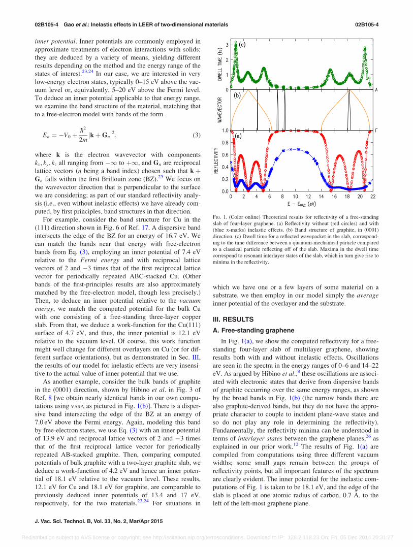
In Fig. 1(a), we show the computed reflectivity for a free-
standing four-layer slab of multilayer graphene, showing
results both with and without inelastic effects. Oscillations
are seen in the spectra in the energy ranges of 0–6 and 14–22
eV. As argued by Hibino et al.,8 these oscillations are associ-
ated with electronic states that derive from dispersive bands
of graphite occurring over the same energy ranges, as shown
by the broad bands in Fig. 1(b) (the narrow bands there are
also graphite-derived bands, but they do not have the appro-
priate character to couple to incident plane-wave states and
so do not play any role in determining the reflectivity).
Fundamentally, the reflectivity minima can be understood in
terms of interlayer states between the graphene planes,26 as
explained in our prior work.12 The results of Fig. 1(a) are
compiled from computations using three different vacuum
widths; some small gaps remain between the groups of
reflectivity points, but all important features of the spectrum
are clearly evident. The inner potential for the inelastic com-
putations of Fig. 1 is taken to be 18.1 eV, and the edge of the
slab is placed at one atomic radius of carbon, 0.7 A, to the
left of the left-most graphene plane.
FIG. 1. (Color online) Theoretical results for reflectivity of a free-standing
slab of four-layer graphene. (a) Reflectivity without (red circles) and with
(blue x-marks) inelastic effects. (b) Band structure of graphite, in (0001)
direction. (c) Dwell time for a reflected wavepacket in the slab, correspond-
ing to the time difference between a quantum-mechanical particle compared
to a classical particle reflecting off of the slab. Maxima in the dwell time
correspond to resonant interlayer states of the slab, which in turn give rise to
minima in the reflectivity.
02B105-4 Gao et al.: Inelastic effects in LEER of two-dimensional materials 02B105-4
J. Vac. Sci. Technol. B, Vol. 33, No. 2, Mar/Apr 2015
Redistribution subject to AVS license or copyright; see http://scitation.aip.org/termsconditions. Download to IP: 128.2.118.23 On: Fri, 05 Dec 2014 20:31:27

For the imaginary part of the potential we assume a linear
energy dependence, Vi ¼ 0:4 eVþ 0:06 E. This dependence
is comparable to what is used in the prior work of Krasovskii
et al.18–20 As demonstrated by those authors, Vi will in gen-
eral increase monotonically, although sometimes in a
stepwise manner as new channels for inelastic electron inter-
actions appear as the energy increases. As a first approxima-
tion, we employ this linear dependence of Vi with energy;
the same dependence was used by Flege et al. in Ref. 20. For
multilayer graphene, we have chosen the parameter values in
this linear dependence such that the amplitudes of the reflec-
tivity oscillations in the energy ranges of 0–6 and 14–22 eV
approximately match experiment.9 We use the same parame-
ters in our treatments of graphene on copper and h-BN on
cobalt as described in Secs. III B and III C.
The lower energy range is displayed in more detail in Fig.
2, showing a comparison of theory with experimental results
from various numbers of graphene layers on SiC (these
results qualitatively resemble the situation for free-standing
graphene, as explained in Ref. 12).8,9,11 The inelastic effects
are seen to significantly diminish the peak-to-valley ampli-
tude of the observed oscillations in the 0–6 eV range, to a
peak-to-valley reflectivity variation of �0.05 for the 6 mono-
layer (ML) case. We note that the theoretical prediction in
Fig. 2 for this peak-to-valley variation is somewhat too large
for the 2–4 ML cases. A likely reason for this discrepancy is
that, theoretically, we are modeling only free-standing gra-
phene whereas, experimentally, the graphene is on a SiC
substrate and so electron absorption can occur within the
substrate itself. The inelastic effects are even larger for the
oscillations in the 14–22 eV range; these just barely visible
in Fig. 1(a), in agreement with experimental results of
Hibino et al.9 Overall, the inclusion of inelastic effects
greatly improves the agreement between theory and experi-
ment for the LEER spectrum.
To further illustrate the inelastic effects, we display in
Fig. 1(c) the computed dwell time for the electron wave-
packets in the slab. The dwell times show marked increases
at energies corresponding to the minima in the reflectivity.
These energies correspond to the interlayer states; as dis-
cussed both by Merzbacher and in Sec. II, at these energies,
the electrons spend more time “bouncing to and fro” in the
slab, producing attenuation in the reflectivity.21 This attenua-
tion extends out to neighboring energies through the mixing
of the states in the slab, as expressed by Eq. (2). We note
that the peak values of dwell time in Fig. 1(c), about 3 fs, are
moderate in size compared to other systems discussed below.
For graphene on Cu(111), we find much smaller dwell times,
whereas for h-BN on various metals we find much larger
ones. In all cases, the magnitudes of the dwell times are
correlated with the widths of the relevant resonant states.
Figure 3 shows the relative insensitivity of our model to
variations in the parameters. First in Fig. 3(a), we vary the
inner potential, using values of V0 ¼ 1 eV or 50 eV rather
than the nominal 18.1 eV. We find that the results are
extremely insensitive to the V0 value; even using V0 ¼ 0 eV
produces nearly the same result except at energies< 1 eV
where a noticeable drop in reflectivity occurs. In practice, an
inner potential value of �10 eV can be used in our model,
for all materials, with negligible error in the results. In
Fig. 3(b), we illustrate the effect of varying the position of
FIG. 2. (Color online) Theoretical (left) and experimental (right) results for
reflectivity of free-standing slab of multilayer graphene of various thick-
nesses in monolayers (ML) as indicated. The absolute reflectivity scale for
the 2 ML case is shown on the left, with subsequent curves shifted upwards
by 0.3 units each.
FIG. 3. (Color online) Theoretical results for reflectivity of a free-standing
slab of four-layer graphene, illustrating the dependence on parameters in the
computation: (a) variation of inner potential V0, (b) variation in the location
of the edge of the slab relative to the left-most plane of carbon atoms, DzE,
and (c) variation in the imaginary portion of the potential.
02B105-5 Gao et al.: Inelastic effects in LEER of two-dimensional materials 02B105-5
JVST B - Nanotechnology and Microelectronics: Materials, Processing, Measurement, and Phenomena
Redistribution subject to AVS license or copyright; see http://scitation.aip.org/termsconditions. Download to IP: 128.2.118.23 On: Fri, 05 Dec 2014 20:31:27
the edge of the slab, using values of 0.35 and 1.4 A to the
left of the graphene plane rather than the nominal 0.7 A. A
fairly small influence on the final result is found (use of the
0.35 A values causes the dwell times to shift �0.02 fs down-
wards, whereas the 1.4 A value shifts them �0.05 fs
upwards). Finally, in Fig. 3(c), we illustrate the influence of
changing the magnitude of the imaginary part of the poten-
tial. Significant changes do now occur in the spectrum, as
expected. All LEED theories to date use the imaginary part
of the potential as a fitting parameter, chosen to match
experiment. The value employed here of Vi ¼ 0:4 eV
þ0:06 E, based in part on the work of Krasovskii et al.,18–20
is found to provide at least a semiquantitative description of
spectra for many different materials. Fine-tuning of these
values can be done in specific cases to produce improved
agreement if necessary.
B. Graphene on copper
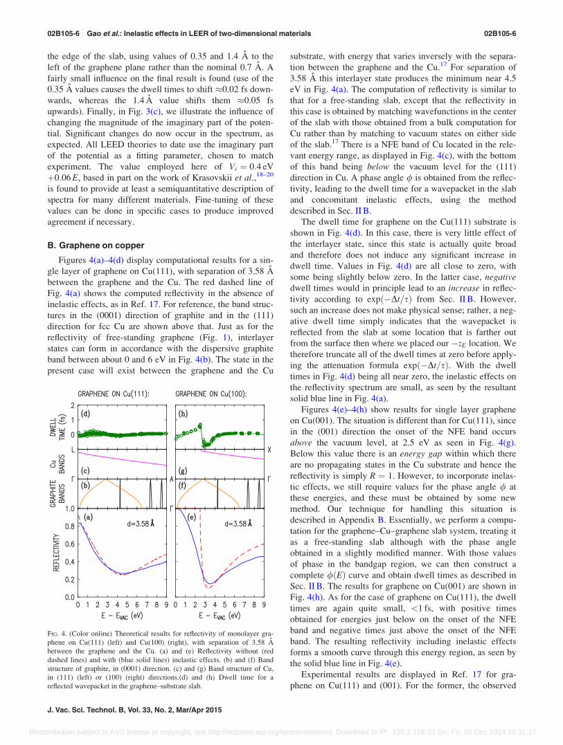
Figures 4(a)–4(d) display computational results for a sin-
gle layer of graphene on Cu(111), with separation of 3.58 A
between the graphene and the Cu. The red dashed line of
Fig. 4(a) shows the computed reflectivity in the absence of
inelastic effects, as in Ref. 17. For reference, the band struc-
tures in the (0001) direction of graphite and in the (111)
direction for fcc Cu are shown above that. Just as for the
reflectivity of free-standing graphene (Fig. 1), interlayer
states can form in accordance with the dispersive graphite
band between about 0 and 6 eV in Fig. 4(b). The state in the
present case will exist between the graphene and the Cu
substrate, with energy that varies inversely with the separa-
tion between the graphene and the Cu.17 For separation of
3.58 A this interlayer state produces the minimum near 4.5
eV in Fig. 4(a). The computation of reflectivity is similar to
that for a free-standing slab, except that the reflectivity in
this case is obtained by matching wavefunctions in the center
of the slab with those obtained from a bulk computation for
Cu rather than by matching to vacuum states on either side
of the slab.17 There is a NFE band of Cu located in the rele-
vant energy range, as displayed in Fig. 4(c), with the bottom
of this band being below the vacuum level for the (111)
direction in Cu. A phase angle / is obtained from the reflec-
tivity, leading to the dwell time for a wavepacket in the slab
and concomitant inelastic effects, using the method
described in Sec. II B.
The dwell time for graphene on the Cu(111) substrate is
shown in Fig. 4(d). In this case, there is very little effect of
the interlayer state, since this state is actually quite broad
and therefore does not induce any significant increase in
dwell time. Values in Fig. 4(d) are all close to zero, with
some being slightly below zero. In the latter case, negativedwell times would in principle lead to an increase in reflec-
tivity according to expð�Dt=sÞ from Sec. II B. However,
such an increase does not make physical sense; rather, a neg-
ative dwell time simply indicates that the wavepacket is
reflected from the slab at some location that is farther out
from the surface then where we placed our �zE location. We
therefore truncate all of the dwell times at zero before apply-
ing the attenuation formula expð�Dt=sÞ. With the dwell
times in Fig. 4(d) being all near zero, the inelastic effects on
the reflectivity spectrum are small, as seen by the resultant
solid blue line in Fig. 4(a).
Figures 4(e)–4(h) show results for single layer graphene
on Cu(001). The situation is different than for Cu(111), since
in the (001) direction the onset of the NFE band occurs
above the vacuum level, at 2.5 eV as seen in Fig. 4(g).
Below this value there is an energy gap within which there
are no propagating states in the Cu substrate and hence the
reflectivity is simply R ¼ 1. However, to incorporate inelas-
tic effects, we still require values for the phase angle / at
these energies, and these must be obtained by some new
method. Our technique for handling this situation is
described in Appendix B. Essentially, we perform a compu-
tation for the graphene–Cu–graphene slab system, treating it
as a free-standing slab although with the phase angle
obtained in a slightly modified manner. With those values
of phase in the bandgap region, we can then construct a
complete /ðEÞ curve and obtain dwell times as described in
Sec. II B. The results for graphene on Cu(001) are shown in
Fig. 4(h). As for the case of graphene on Cu(111), the dwell
times are again quite small, <1 fs, with positive times
obtained for energies just below on the onset of the NFE
band and negative times just above the onset of the NFE
band. The resulting reflectivity including inelastic effects
forms a smooth curve through this energy region, as seen by
the solid blue line in Fig. 4(e).
Experimental results are displayed in Ref. 17 for gra-
phene on Cu(111) and (001). For the former, the observed
FIG. 4. (Color online) Theoretical results for reflectivity of monolayer gra-
phene on Cu(111) (left) and Cu(100) (right), with separation of 3.58 A
between the graphene and the Cu. (a) and (e) Reflectivity without (red
dashed lines) and with (blue solid lines) inelastic effects. (b) and (f) Band
structure of graphite, in (0001) direction. (c) and (g) Band structure of Cu,
in (111) (left) or (100) (right) directions.(d) and (h) Dwell time for a
reflected wavepacket in the graphene–substrate slab.
02B105-6 Gao et al.: Inelastic effects in LEER of two-dimensional materials 02B105-6
J. Vac. Sci. Technol. B, Vol. 33, No. 2, Mar/Apr 2015
Redistribution subject to AVS license or copyright; see http://scitation.aip.org/termsconditions. Download to IP: 128.2.118.23 On: Fri, 05 Dec 2014 20:31:27

reflectivity minimum is quite broad, in agreement with our
theoretical result including inelastic effects. For the latter
case, the smooth variation in reflectivity through the onset of
the NFE band is also in general agreement with experiment,
although the absolute magnitude of the reflectivity in the
experiment is somewhat smaller than obtained in the theory.
However, those experiments were obtained from samples
that had been exposed to air for times ranging from several
days to several weeks, and the reflectivity in the bandgap
region showed a significant decrease with the exposure
time.17 Oxidation of the Cu surface is thus seen to modify
the spectrum. Future acquisition of a spectrum from a
non–air-exposed surface is needed in order to achieve a
more detailed comparison between experiment and theory.
C. Hexagonal boron nitride on cobalt
For the situations discussed above, the inelastic effects
have been moderate or small, with dwell times of a few
femtoseconds or less. We now turn to the case of h-BN on
metal substrates such as Co or Ni, for which the inelastic
effects are found to be quite large, with dwell times of 10’s
of femtoseconds or more. Reflectivities that are near unity
in the absence of inelastic effects can thus be attenuated to
<0.1 when nearby bands with long dwell times are present.
Thus, inclusion of the inelastic effects becomes quite impor-
tant in the interpretation of the spectra. Experimental LEER
spectra for h-BN on Co have been previously presented by
Orofeo et al.,27 and these were qualitatively compared with
a computed h-BN band structure. We present here theoreti-
cally obtained LEER spectra, from which a more detailed
interpretation of all the various spectral features can be
made.
Separately, we have performed detailed experimental and
theoretical LEER studies for h-BN on Ni.28 One important
result of those studies is that oxidation of the Ni surface (due
to air exposure for at least several days between sample
growth and introduction into the LEEM chamber) plays an
important role in the experimental LEER spectra. LEED
measurements have directly revealed the presence of this ox-
ide.28 The oxide produces a dipole at the interface, thus
increasing the work function of the surface and shifting the
onset of the Ni NFE bands from a location about 3 eV above
the vacuum level to a location slightly below the vacuum
level; this shift, in turn, significantly impacts the predicted
LEER spectra. For our theoretical results of h-BN on Co, we
similarly employ an oxide at the interface.
Figure 5 displays computed LEER spectra for h-BN on
the oxidized Co(0001) surface. The computations employ a
five-layer hcp Co slab, together with oxygen and h-BN
layers on either side. The O-Co separation is chosen to be
1.1 A, obtained from a first-principles relaxation of a bare O
layer on the Co surface. The BN-O separation is taken to be
1.68 A, chosen in order to approximately match the theory
with the experimental results of Orofeo et al.27 For this value
of BN-O separation the reflectivity minimum for a single
h-BN layer occurs at about 7.5 eV, compared to 6.5 eV in
the experiment. With a subsequent h-BN layer, a minimum
appears near 2 eV, comparable to the experiment. In the
theoretical spectra of Fig. 5, we show results for both the
majority and minority spin, with onsets of the Co NFE bands
being at 1.0 and 2.0 eV above the vacuum level, respec-
tively. The average of the spin-resolved reflectivity curves,
for each thickness of h-BN, can be compared to the experi-
mental spectra (which are not spin resolved).27
Good agreement is obtained between the theoretical spec-
tra and the experimental results of Orofeo et al.27 Just as for
the case of graphene, interlayer states form between the h-
BN layers, with n� 1 of these states forming for n layers of
h-BN.12,27 There are three relevant bands of the h-BN that
occur over the energy range shown in Fig. 5, and for each of
these bands there will, in principle, be n� 1 reflectivity min-
ima. These n� 1 bands are seen for the elastic results for the
highest h-BN band in Fig. 5, although for the middle band
they are not well resolved due to the energy-resolution of the
computations. For the lowest band some of the minima are
FIG. 5. (Color online) (a)–(d) Theoretical results for reflectivity of 1–4 layer
h-BN on oxidized Co (0001) surface, with separation of 1.1 A between the
O and Co, 1.68 A between BN and O, and 3.3 A between BN layers.
Reflectivity without (dashed lines) and with (solid lines) inelastic effects.
Black and gray (red) are for majority and minority spins, respectively. (e)
Dwell time for four-layer h-BN on oxidized Co as in (d), majority spin. (f)
h-BN band structure. (g) Co band structure. Black is majority spin, and red
is minority spin.
02B105-7 Gao et al.: Inelastic effects in LEER of two-dimensional materials 02B105-7
JVST B - Nanotechnology and Microelectronics: Materials, Processing, Measurement, and Phenomena
Redistribution subject to AVS license or copyright; see http://scitation.aip.org/termsconditions. Download to IP: 128.2.118.23 On: Fri, 05 Dec 2014 20:31:27

cut off in the elastic results due to the fact that the onsets of
the NFE band lie above the vacuum level, but they are none-
theless clearly seen in the inelastic results. For the case of a
single layer of h-BN, the relatively small BN-O separation
precludes the presence of a well-defined interlayer state
between those layers, with the resulting elastic spectrum
displaying a broad minimum near 9 eV and a maximum
near 7 eV.
Importantly, inclusion of inelastic effects has a pro-
found influence on the spectra for all the h-BN thicknesses.
In panel (e) of Fig. 6, we display dwell times for the case
of four h-BN monolayers. Relatively large dwell times are
found, particularly for the band centered at 6.8 eV. These
dwell times produce low reflectivity for that band, and
importantly, due to the mixing between nearby eigenstates
that we employ in our model, this attenuation is then
spread out to neighboring eigenstates that have high reflec-
tivity in the absence of inelastic effects. Whereas a maxi-
mum occur in the elastic spectra at about 7 eV (for 1 ML
h-BN) or 8 eV (for 2–4 ML h-BN), the inelastic effects
produce sufficiently strong attenuation such that a mini-mum (for 1 ML) or very weak local maxima (for 2–4 ML)
are produced in the spectra at these energies. Our interpre-
tation of the spectra is in agreement with that presented
previously by Orofeo et al.,27 with our predicted reflectiv-
ity curves enabling a much more detailed understanding of
the various spectral features. Again, proper treatment of
inelastic effects is essential in producing spectra that can
be compared to experiment.
IV. SUMMARY
In summary, we have presented a model for including
inelastic effects into our computational methodology for
low-energy electron reflectivity from surfaces. The model
contains two components, one of which is rigorous (the
dwell time for an electron in a slab) and the other approxi-
mate (the mixing between single-particle states in the slab).
Our model is therefore not rigorously defined, both because
of its approximate component and due to the way in which
we have split the problem into two separable parts.
However, we find from applying the model to a range of sit-
uations that we obtain results which are in reasonably good
agreement with experiment. Additionally, the model can be
easily incorporated into our reflectivity analysis method (i.e.,
using many of the same numerical quantities that are avail-
able in that procedure), so in this way it represents a useful
advancement in the methodology. As illustrated in this work,
inclusion of the inelastic effects permits detailed comparison
between experimental and theoretical LEER spectra, from
which structural parameters for the surface under study can
be deduced.
ACKNOWLEDGMENTS
This work was supported by the National Science
Foundation under Grant No. DMR-1205275 and the Office of
Naval Research under MURI Grant No. N00014-11-1-0678.
APPENDIX A
Here, we provide details of an improved method for
dealing with the “mixed” states discussed in Ref. 12 that
act to couple slabs in adjoining simulation cells. To intro-
duce this topic, we first review the basic properties of
reflected or diffracted waves as described in Ref. 12.
We initially consider a slab of material with a semi-
infinite expanse of vacuum on either side. In that case,
denoting the direction perpendicular to the slab surface
by z, then the wavefunction in the vacuum for a propagat-
ing state with energy E will consist of a traveling
wave expðijgzÞ multiplied by a sum of lateral waves
of the form Ag exp½i ðgxxþ gyyÞ�. Here, the lateral
wavevector is g ¼ ðgx; gyÞ, Ag is an amplitude, jg ¼ffiffiffiffiffiffiffiffiffiffiffiffiffiffiffiffiffiffiffiffiffiffiffiffiffiffiffiffiffiffiffiffiffiffiffiffiffiffiffiffiffiffiffiffiffiffiffiffiffiffiffi2mðE� EVÞ=�h2 � g2
x � g2y
qis the z-component of the
wavevector in the vacuum, EV is the vacuum energy, and mis the free-electron mass. Diffracted beams have ðgx; gyÞ6¼ ð0; 0Þ; these exist only for E� EV � �h2ðg2
x þ g2yÞ=2m. Of
course, at lower energies, evanescent states with substantial
ðgx; gyÞ 6¼ ð0; 0Þ character exist; they extend out from the
slab surface. These states decay to zero as the distance into
the vacuum approaches infinity, so the amplitude of their
ðgx; gyÞ ¼ ð0; 0Þ component far into the vacuum is zero.
Now let us turn to the periodically repeating vacuum–-
slab–vacuum geometry of our VASP computation. With the
finite vacuum width, the evanescent states cannot possibly
decay exactly to zero, and as a consequence, all such states
FIG. 6. (Color online) Computed energy bands for four layers of graphene,
with simulation cell widths of (a) 4.0266 nm, (b) 5.3688 nm, and (c)
6.711 nm. Energy bands of bulk graphite are shown in (d). The wavevector
(kz) ranges in (a)–(c) are given by p divided by the cell width, whereas in
(d) the wavevector varies from the C-point to the A-point. Energies in
(a)–(c) are plotted relative to the vacuum level of each slab, whereas in (d)
the bulk band is positioned by aligning the potential of the bulk with the
potential of the four-layer slab in (a). The colors of the bands in (a)–(c) is
chosen to coincide with those of Fig. 7.
02B105-8 Gao et al.: Inelastic effects in LEER of two-dimensional materials 02B105-8
J. Vac. Sci. Technol. B, Vol. 33, No. 2, Mar/Apr 2015
Redistribution subject to AVS license or copyright; see http://scitation.aip.org/termsconditions. Download to IP: 128.2.118.23 On: Fri, 05 Dec 2014 20:31:27

acquire a small, nonzero ðgx; gyÞ ¼ ð0; 0Þ component in
the vacuum. In practice, the magnitude of this nonzero
ðgx; gyÞ ¼ ð0; 0Þ component can be much greater than what
would arise, e.g., simply from extrapolating the exponen-
tially decaying part of the wavefunction out to the edge of
the vacuum region. Such states are said to have “mixed”
character; they exist at energies less than �h2ðg2x þ g2
yÞ=2mand have primarily ðgx; gyÞ 6¼ ð0; 0Þ character, but they do
not decay to zero in the vacuum. Examples of such states are
shown in Figs. 3(a) and 3(b) of Ref. 16. For these mixedstates, we find that the magnitude of their ðgx; gyÞ ¼ ð0; 0Þcomponent in the vacuum varies with the vacuum width
used in the simulation. In this sense, the states are spurious;
their ðgx; gyÞ ¼ ð0; 0Þ component is an artifact of the finite
cell size used in the simulation. Importantly, the nonzero
ðgx; gyÞ ¼ ð0; 0Þ character of these states will, if used in our
reflectivity analysis, lead to some reflectivity associated with
these states. Those reflectivity values are themselves arti-
facts, and hence, these mixed evanescent states must some-
how be rejected from the analysis.
In order to identify the mixed states, we have in our prior
work employed the quantity r defined in the supplementary
material of Ref. 12, which is the overlap in the vacuum
between the wavefunction of a state and a simple oscillatory
wavefunction expected for a free electron states. Values of rare generally small (�10�2) for spurious mixed states and
large (�1) for bona fide propagating states. Importantly,
since our definition of r includes a scale factor relating to
the width of the vacuum region, then for the bona fide propa-
gating states, their r values necessarily approach unity for
sufficiently large vacuum width (this point is further dis-
cussed at the end of this Appendix). However, for certain
mixed states we occasionally find r values of 0.1 or greater,
so separating them from the bona fide states can become
problematic. In our previous work we employed a discrimi-
nator value of r ¼ 0:8, rejecting all states with smaller rvalues.12 Although that value worked reasonably well for the
multilayer graphene case, we find in other cases that this dis-
criminator value can sometimes lead to rejection of bonafide propagating states, something that is important to avoid
especially when inelastic effects are included. We have
therefore employed in the present analysis a smaller discrim-
inator value, r ¼ 0:1, but we supplement that by detailed
inspection of the results, including their dependence on the
vacuum width of the simulation. In this way, we can further
reject the occasional state that is identified as having mixed
character but which nevertheless has a r value of 0.1 or
greater.
To illustrate this procedure, we display in Fig. 6 a small
energy window for a simulation involving a free-standing
slab of four graphene layers, with three different vacuum
widths corresponding to total simulation cell widths of
4.0266, 5.3688, and 6.711 nm (the vacuum width is given by
these values minus the width of the four-layer graphene slab,
1.0 nm). We choose the energy window to correspond to the
location of the narrow bulk graphite band centered at about
7.25 eV as seen in the band structures of Figs. 1 and 4. We
plot the energy of eigenstates in the respective slab
computations in Figs. 6(a)–6(c), with the narrow bulk
band shown for reference in Fig. 6(d). The eigenstates in
Figs. 6(a)–6(c) are separated into bands, labeled 1–5 in each
panel. It is clear that there is one dispersive band, e.g.,
labeled 1 in Fig. 6(a), and four nearly flat bands. The disper-
sive band is associated with a propagating states in the
vacuum; it moves up in energy as the simulation width
increases, simply reflecting the location of the allowed
energy window for propagating states of our periodic vac-
uum–slab–vacuum system. In each of Figs. 6(b) and 6(c),
the dispersive band crosses a flat band, resulting in band
anticrossing behavior.
The states associated with the flat bands (or flat portions
of bands) in Fig. 6 are all of the “mixed” type defined above,
that is, they have large, in-plane oscillatory nature in the gra-
phene planes, with very small (but constant, as a function
of z) ðgx; gyÞ ¼ ð0; 0Þ component far out in the vacuum. In
particular, for Fig. 6(a), the wavefunctions of bands 2 and 3
at the midpoint of the wavevector range are identical to those
shown in Figs. 3(a) and 3(b) of Ref. 16 (the energies in the
present computation have been updated slightly compared to
those of Ref. 16, but nevertheless the wavefunctions shown
in Ref. 16 are identical to those of the present computa-
tion).29 In contrast, the wavefunction associated with the dis-
persive band in Fig. 6(a) has character more like Fig. 3(c) of
Ref. 16, i.e., with substantial ðgx; gyÞ ¼ ð0; 0Þ component
both in the vacuum and in the slab.
In Fig. 7, we plot the r values for all the slab states asso-
ciated with the computations of Fig. 6, using a wide energy
range of 0–20 eV but with expanded view of the 6.9–7.4 eV
range of Fig. 6. Clearly, two ranges of r values are domi-
nant: near unity (which are the bona fide propagating states),
and �10�2 (which are all spurious mixed states). However, a
few intermediate values also occur, and furthermore, and
these intermediate r values are not associated with a state at
a fixed energy as we vary the simulation cell width. By com-
parison of Figs. 6 and 7, the intermediate r values lying
between 0.1 and about 0.8 can be seen to occur when the
FIG. 7. (Color online) Plot of the magnitude of the oscillatory component of
the wavefunction in the vacuum, r, as a function of the energy of the states,
for the same simulation cells (a)–(c) used in Fig. 6. Different colors are used
to represent different bands. Dashed lines are drawn in each panel at r val-
ues of 0.1 and 0.8. Note the expanded energy scale over 6.9–7.4 eV.
02B105-9 Gao et al.: Inelastic effects in LEER of two-dimensional materials 02B105-9
JVST B - Nanotechnology and Microelectronics: Materials, Processing, Measurement, and Phenomena
Redistribution subject to AVS license or copyright; see http://scitation.aip.org/termsconditions. Download to IP: 128.2.118.23 On: Fri, 05 Dec 2014 20:31:27

energy of the dispersive band is near, or crossing, the energy
of a flat band. At such band crossings (anticrossings), inter-
action between the states in the bands leads to larger r val-
ues for the mixed states. Similar band crossings account for
the intermediate r values at all other energies in Fig. 7.
We therefore reject states that have intermediate r values
resulting from this interaction between the mixed and propa-
gating states. For example, band 2 in Figs. 6(a) and 7(a)
acquires some increased r value due to its proximity to band
1. Hence, all states in band 2 are rejected (even though one
state in that band has a r value of >0.1). The situation for
the band anticrossings in Figs. 6(b) and 7(b) and in Figs. 6(c)
and 7(c) is slightly more complicated. We could simply
reject all of the states in bands 1 and 2 for the former case
and bands 2 and 3 for the latter, which would certainly elimi-
nate all spurious states, but we would then end up eliminat-
ing a few bona fide states as well (i.e., on the dispersing ends
of the respective bands). Thus, we choose to reject only
those portions of the bands with states having r values of
<0:1, along with a few nearby states in each band that have
r values between 0.1 and about 0.8.
The situation just described for multilayer graphene slabs
is actually a relatively easy one, since the r-separation
between propagating and evanescent states is straightforward
to discern and the mixed states can be readily dealt with. In
general, the ease with which this analysis can be conducted
depends on both the nature of the states in the slab and the
width of the vacuum region in the simulation. If we were to
display in Fig. 7 results for the multilayer graphene for
smaller simulation cell width (e.g., �2.5 nm), then the sepa-
ration of the bona fide and mixed states would be much less
clear; in particular, many of the bona fide states would have
r values significantly less than unity. Again, since our defini-
tion of r includes a scale factor relating to the width of the
vacuum region, then for bona fide states, their r values
always approach unity for sufficiently large vacuum width.
For example, consider a state that has much of its wavefunc-
tion concentrated in the slab, but that nevertheless has a
small (nonspurious) tail with ðgx; gyÞ ¼ ð0; 0Þ character
extending out into the vacuum. Such states do not occur for
multilayer graphene because of the nature of its states (i.e.,
the narrow bands of graphite shown in Figs. 1 and 4 all have
in-plane oscillatory nature with essentially zero ðgx; gyÞ ¼ð0; 0Þ character), but for h-BN, with its inequivalent B and N
atoms, such states do occur (and they do contribute to the
reflectivity) since some of its narrow bands acquire some
nonzero ðgx; gyÞ ¼ ð0; 0Þ character. How then do we distin-
guish between spurious and bona fide states in this case? The
answer, as just stated, is that even these bona fide states with
relatively small ðgx; gyÞ ¼ ð0; 0Þ character in the vacuum
have r values that approach unity for sufficiently large vac-
uum width. A unity value of r, as a function of increasing
vacuum width, implies that the ratio of the wavefunction
magnitude in the vacuum compared to that within the slab is
constant, i.e., as expected when the propagating part of the
wavefunction in the vacuum is a true, invariant feature.
Conversely, if a state maintains a low r value, e.g., <0.1, as
a function of increasing vacuum width, then that implies that
its wavefunction magnitude in the vacuum is actually
decreasing relative to that within the slab. This varying ratio
of wavefunction magnitude in the vacuum compared to
within the slab (i.e., an overall decrease as a function of
increasing vacuum width, together with fluctuations due to
the presence of nearby propagating states) is the hallmark of
a spurious, mixed state.
APPENDIX B
Here, we provide details of the method used to deduce
scattering phase shifts for an overlayer on a substrate for the
situation when the energy of the incident electron falls
within a bandgap for the electronic states of the substrate.
An important distinction should be made between the
approximate method that we employ for our reflectivity anal-
ysis compared to the more rigorous computation of
Krasovskii et al.18,19 Those authors use a semi-infinite model
for the substrate, computing its states for both real and imag-
inary values of the wavevector kz. Within a bandgap region,
no eigenstates exist for purely real values of kz, but evanes-cent states corresponding to imaginary kz values do naturally
occur. It is these evanescent states that will couple to an inci-
dent electron wave that has propagated through the over-
layer, and the phase shift in the reflected wave relative to the
incident one is determined by the evanescent states. In our
approximate model, we do not compute these evanescent
states for the bulk substrate. Rather, we first perform a super-
cell computation for a vacuum–overlayer–substrate–over-
layer–vacuum system with a substrate of limited thickness
(typically only a few atomic layers), and then we match
states of that system to states of a periodic (infinite) bulk
substrate with only real kz values. Thus, we do not obtain
evanescent states of our bulk substrate and hence these are
not available for the purpose of determining the phase of the
reflected wave.
However, since we compute the spectrum of states for the
vacuum-overlayer-substrate-overlayer-vacuum supercell, we
do obtain some information on evanescent states of the bulk
substrate. That is, even with purely real kz values, that slab
computation will include states that exist for energies within
the bandgap of the bulk substrate. These states will vary
exponentially with distance (decaying or growing) within
the substrate portion of the slab, for energies in the bandgap.
From these states, we wish to construct a linear combination
that has purely decaying exponential behavior in the sub-
strate portion of the slab.
In our general methodology for reflectivity analysis of a
free-standing slab,12 we construct linear combinations of
states that are even or odd relative to the center of the slab
(assuming, for ease of discussion, a potential that is symmet-
ric about this central point). In the vacuum region on the far
left-hand side of the simulation cell these functions vary like
Ae cosðkzþ deÞ and Ao sinðkzþ doÞ, respectively, thus defin-
ing de and do. On the far right-hand side of the simulation
cell, they vary like Ae cosðkz� d0eÞ and Ao sinðkz� d0oÞ,thus defining d0e and d0o, and with de ¼ d0e and do ¼ d0o for
a symmetric potential. In our standard method, we form
02B105-10 Gao et al.: Inelastic effects in LEER of two-dimensional materials 02B105-10
J. Vac. Sci. Technol. B, Vol. 33, No. 2, Mar/Apr 2015
Redistribution subject to AVS license or copyright; see http://scitation.aip.org/termsconditions. Download to IP: 128.2.118.23 On: Fri, 05 Dec 2014 20:31:27

further linear combinations such that on the right-hand side
of the slab there is only an outgoing wave, whereas on the
left-hand side there are both incoming and outgoing waves.
In that way, the transmission coefficient is found to be (see
supplementary material of Ref. 12)
T ¼ 2 cos d0e � d0oð Þei d0eþdoð Þ þ ei deþd0oð Þ
��������2
: (B1)
Examining this result, we see that in order to achieve T ¼ 0
(i.e., reflectivity of R ¼ 1), then we must have d0e � d0o¼ p=2 or 3p=2, modulo 2p. If this situation occurs for an
energy lying within a bandgap in the bulk electronic spec-
trum, then we would have achieved our goal of constructing
a purely exponentially decaying state within the substrate
portion of the slab (since its amplitude is clearly going to
zero on the right-hand side of the slab).
However, for energies within a bandgap we will not in
general find R ¼ 1 in our analysis of the free-standing slab.
In these cases, we still desire to minimize the amplitude of
the wavefunction on the right-hand side of the slab. For this
purpose, we form a slightly different linear combination than
that which was employed for obtaining Eq. (B1). Rather
than demanding that the incoming wave on the right-hand
side of the slab be zero, we instead desire to minimize the
amplitude of both the incoming and outgoing waves on the
right-hand side of the slab. Consider forming in the vacuum
region on the right-hand side of the slab the combination
AoAe cosðkz� d0eÞ6AeAo sinðkz� d0oÞ: (B2)
When d0e � d0o ¼ p=2 or 3p=2 then this combination is zero
when using the lower or upper sign, respectively. However,
even when d0e � d0o deviates slightly away from p=2 or
3p=2 then the combination is still small. The reason that it is
small is that, within the substrate portion of the slab, the lin-
ear combination [Eq. (B2)] approximately takes a form pro-
portional to AoAecoshðkzÞ � AeAosinhðkzÞ,30 leading to a
purely exponentially decaying dependence for z > 0. Given
this linear combination [Eq. (B2)], then the ratio of reflected
to incident waves on the left-hand side of the slab is easily
found to be ðe�ide 6 e�idoÞ=ðeide 7 eidoÞ. The phase / of this
complex quantity then gives us the phase angle to use in our
dwell time analysis, for energies within a bulk bandgap.
As a test of the applicability of the linear combination
[Eq. (B2)] for forming states on the right-hand side of the
slab that have small amplitude, we consider the amount by
which d0e � d0o deviates away from p=2 or 3p=2. For the
cases considered in the body of this work with substrate
thicknesses of three or five atomic layers, we generally
obtained deviations of less than 0.1, for which we consider
the resulting / values to be sufficiently accurate since they
do not significantly change even if a thicker substrate portion
of the slab is employed. In situations where the deviation is
larger, then we redo the analysis using a thicker substrate
portion of the slab, in order to decrease the deviation in
d0e � d0o away from p=2 or 3p=2.
1F. Jona, J. Phys. C: Solid State Phys. 11, 4271 (1978), and references
therein.2M. A. Van Hove, W. Moritz, H. Over, P. J. Rous, A. Wander, A. Barbieri,
N. Materer, U. Starke, and G. A. Somorjai, Surf. Sci. Rep. 19, 191 (1993).3H. L€uth, Surface and Interfaces of Solid Materials, 3rd ed. (Springer, New
York, 1995).4R. Zdyb and E. Bauer, Phys. Rev. Lett. 88, 166403 (2002).5B. T. Jonker, N. C. Bartelt, and R. L. Park, Surf. Sci. 127, 183 (1983).6W. F. Chung, Y. J. Feng, H. C. Poon, C. T. Chan, S. Y. Tong, and M. S.
Altman, Phys. Rev. Lett. 90, 216105 (2003).7M. Altman, J. Phys.: Condens. Matter 17, S1305 (2005).8H. Hibino, H. Kageshima, F. Maeda, M. Nagase, Y. Kobayashi, and H.
Yamaguchi, Phys. Rev. B 77, 075413 (2008).9H. Hibino, H. Kageshima, F. Maeda, M. Nagase, Y. Kobayashi, and H.
Yamaguchi, e-J. Surf. Sci. Nanotech. 6, 107 (2008).10P. Sutter, J. T. Sadowski, and E. Sutter, Phys. Rev. B 80, 245411 (2009).11Luxmi, N. Srivastava, and R. M. Feenstra, J. Vac. Sci. Technol., B 28,
C5C1 (2010).12R. M. Feenstra, N. Srivastava, Q. Gao, M. Widom, B. Diaconescu, T.
Ohta, G. L. Kellogg, J. T. Robinson, and I. V. Vlassiouk, Phys. Rev. B 87,
041406(R) (2013), and references therein.13G. Kresse and J. Hafner, Phys. Rev. B 47, 558 (1993).14G. Kresse and J. Furthmuller, Phys. Rev. B 54, 11169 (1996).15G. Kresse and D. Joubert, Phys. Rev. B 59, 1758 (1999).16R. M. Feenstra and M. Widom, Ultramicroscopy 130, 101 (2013).17N. Srivastava, Q. Gao, M. Widom, R. M. Feenstra, S. Nie, K. F. McCarty,
and I. V. Vlassiouk, Phys. Rev. B 87, 245414 (2013).18E. E. Krasovskii, W. Schattke, V. N. Strocov, and R. Claessen, Phys. Rev. B
66, 235403 (2002).19E. E. Krasovskii and V. N. Strocov, J. Phys.: Condens. Matter 21, 314009
(2009).20J. Ingo Flege, A. Meyer, J. Falta, and E. E. Krasovskii, Phys. Rev. B 84,
115441 (2011).21E. Merzbacher, Quantum Mechanics, 2nd ed. (Wiley, New York, 1970).22D. R. Penn, J. Vac. Sci. Technol. 13, 221 (1976), and references therein.23A. Goswami and N. D. Lisgarten, J. Phys. C: Solid State Phys. 15, 4217
(1982), and references therein.24S. Y. Zhou, G.-H. Gweon, and A. Lanzara, Ann. Phys. 321, 1730 (2006).25C. Kittel, Introduction to Solid State Physics, 8th ed. (Wiley, New York,
2005).26M. Posternak, A. Baldereschi, A. J. Freeman, E. Wimmer, and M.
Weinert, Phys. Rev. Lett. 50, 761 (1983).27C. M. Orofeo, S. Suzuki, H. Kageshima, and H. Hibino, Nano Res. 6, 335
(2013).28P. C. Mende, Q. Gao, M. Widom, and R. M. Feenstra, “Characterization
of hexagonal boron nitride layers on nickel surfaces” (unpublished).29The band structure displayed in Fig. 2 of Ref. 16 is one that was inadver-
tently computed with only 4–5 significant figures used to specify some of
the atomic positions in the unit cell. Nevertheless, all other results in that
work were computed with a full 6–7 significant figures used for all atomic
positions. The energy eigenvalues of 3.24, 7.09, and 7.14 eV specified in
Ref. 16 are shifted to 3.24, 7.16, and 7.22 eV for the higher precision
eigenvalues of the present work.30More generally, the linear combination [Eq. (B2)] in the substrate portion
of the slab would contain cosh(z) and sinh(z) terms as envelope functionsof the complete wavefunction, but this does not change our argument.
02B105-11 Gao et al.: Inelastic effects in LEER of two-dimensional materials 02B105-11
JVST B - Nanotechnology and Microelectronics: Materials, Processing, Measurement, and Phenomena
Redistribution subject to AVS license or copyright; see http://scitation.aip.org/termsconditions. Download to IP: 128.2.118.23 On: Fri, 05 Dec 2014 20:31:27