implementation and application of gate voltage in negf...
TRANSCRIPT

Mari Ohfuchi1 and Taisuke Ozaki21Fujitsu Laboratories Ltd.2Institute for Solid State Physics, The University of Tokyo
Implementation and Application
of Gate Voltage in NEGF
Calculations
2016 COPYRIGHT FUJITSU LABORATORIES LTD.

My 2nd Visit to South Korea This Month
1 2016 COPYRIGHT FUJITSU LABORATORIES LTD.
Nov. 24 − 252nd OpenMX
Developer's MeetingDaejeon, 3 h
Oct. 30 − Nov. 37th A3 Symposium
on Emerging Materials
Buyeo, 2.5 h

Introduction
Motivation and Significance for the Implementation of a Gate Function in NEGF Calculations
Implementation of a Gate Function
Symmetric Zigzag Graphene Nanoribbon Spin Filter
Application to All Two-Dimensional (2D) Tunneling Field Effect Transistors (TFETs)
P-doped GeSe/MoS2/VS2 TFETs
Summary
2
Outline
2016 COPYRIGHT FUJITSU LABORATORIES LTD.

Introduction
3 2016 COPYRIGHT FUJITSU LABORATORIES LTD.
MPUMicro processor unit
MOS (metal oxide semiconductor)
transistor
GLph
MPU High-Performance Physical Gate Length
Non-classical CMOS
High-κ metal gate
High mobility channel materials
Physics-Based Simulation, OpenMX
Dimensional scaling
Equivalent scaling
Tunneling, Spin

Whole device
Toward Whole-Device Simulations
4
20142011
Num
ber
of Ato
ms
10,000
1,000
2016 COPYRIGHT FUJITSU LABORATORIES LTD.
2016
3,000
Appl. Phys. Express 4, 095101 (2011)
Appl. Phys. Express 7, 025101 (2014)
O(N) Parallelization of NEGF calculations
2018
Implementation of Gate Voltage
Implementation of a Gate Function
5
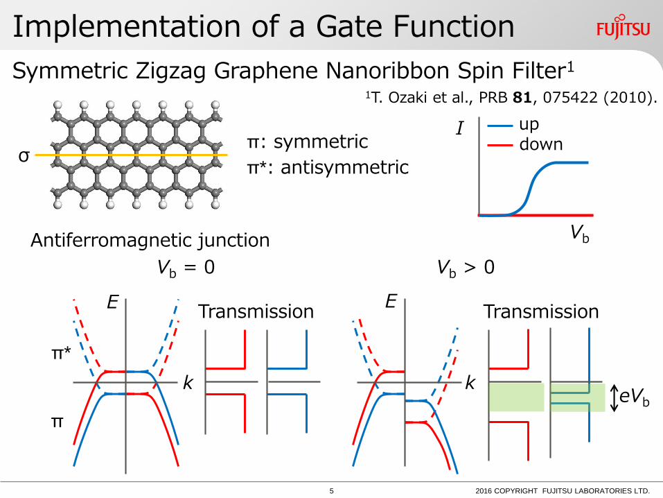
Symmetric Zigzag Graphene Nanoribbon Spin Filter1
2016 COPYRIGHT FUJITSU LABORATORIES LTD.
1T. Ozaki et al., PRB 81, 075422 (2010).
σπ: symmetric
π*: antisymmetric
Antiferromagnetic junction
k
ETransmission
π
π*
k
ETransmission
Vb = 0 Vb > 0
I
Vb
updown
eVb

Model for tests of the implementation
6
z x
y
Symmetric Zigzag Graphene Nanoribbon
2016 COPYRIGHT FUJITSU LABORATORIES LTD.
Ferromagnetic junction
TransmissionVSG < 0
E
Double gate structure

3D Poisson equation
7
Periodic BCOpen BCBoundary condition (BC)
2016 COPYRIGHT FUJITSU LABORATORIES LTD.
Parallelization in bc plane (63x125)
Parallelization in only c line (125)
a (90)
b (63)
c (125)

Programing
8 2016 COPYRIGHT FUJITSU LABORATORIES LTD.
tran_variables.hopenmx_common.hlapack_prototypes.htran_prototypes.hAllocate_Arrays.cFree_Arrays.cinit_alloc_first.ctruncation.c: Preparation for transforming from AB to C partitionTRAN_Input_std.cTRAN_Poisson.c
Modification of only 10 Files
TRAN_Poisson_FDG
Transformation from C to AB partition
FFT for the boundary conditions
Transformation from AB to C partition
2D real space Poisson equation
FFT to real space

Hartree Potential (eV)
9
VSD = 0.3 V, VSG = −10 V
xy
zx
zx
xy
VSD = 0 V, VSG = 0 V
2016 COPYRIGHT FUJITSU LABORATORIES LTD.
z x
y

Transmission
10 2016 COPYRIGHT FUJITSU LABORATORIES LTD.
VSD = 0.3 V, VSG = −10 VVSD = 0 V, VSG = 0 V
E
E
updown
This provides another possible spin filter.
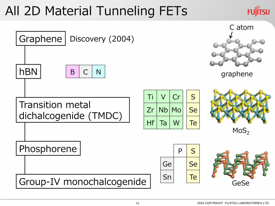
All 2D Material Tunneling FETs
11
Graphene
hBN
Transition metaldichalcogenide (TMDC)
Phosphorene
Group-IV monochalcogenide
Discovery (2004)
C NB graphene
Ta WHf
Nb MoZr
V CrTi
C atom
Te
Se
S
Te
Se
SP
Ge
SnGeSe
MoS2
2016 COPYRIGHT FUJITSU LABORATORIES LTD.

GeSe/MoS2/VS2 Tuneling FETs (TFETs)
12 2015 COPYRIGHT FUJITSU LABORATORIES LTD.
ChannelSource Drain
MoS2
TFET
VS2
The lattices of these materials are matched with a relatively small unit cell.
P-dopedGeSe
The subthreshold swing
(SS) in conventional FETs
is limited to 60 mV/dec.
VSG
ISD
SS

DFT code: OpenMX
Exchange-correlation potential:
GGA-PBE with van der Waals correction
Norm-conserving pseudopotential:
Troullier-Martins
Pseudo atomic orbitals (PAOs)
Geometry optimization:
Ge7.0-s3p3d3f2, Se7.0-s3p3d2f1, P7.0-s3p3d2f1, Mo7.0-s3p2d2f1, S7.0-s3p3d2f1, V6.0-s3p3d2
Transport: s2p2d1
Temperature: T = 300 K
Computational Details
13 2015 COPYRIGHT FUJITSU LABORATORIES LTD.

Atomic Structure
14 2015 COPYRIGHT FUJITSU LABORATORIES LTD.
x
z
x
y
ChannelSource Drain
Gate
Gate
LCh
2.6 nm
GeSe
MoS2
VS2
244
2.6 nm
Numberof atomsLCh
1.9 nm
280
Interlayer distance: 0.323 nmContact length: 0.6 nm

Gate Control
15 2015 COPYRIGHT FUJITSU LABORATORIES LTD.
Partial density of states (PDOS) of Mo atom in the center of the channel (LCh=1.9 nm)
VSD = 0.1 V

Device Properties
16 2015 COPYRIGHT FUJITSU LABORATORIES LTD.
VSD = 0.1 V
SS = 3.6 V/dec@LCh = 2.6 nm
SS =8.5 V/dec@LCh = 1.9 nm
> 10
2.6 nm
Ion/IoffLCh
1.9 nm
> 103
The subthreshold swing (SS) would be further improved by using a high-κ material as a gate dielectric that is a vacuum in the present model.

Computational Cost
17 2015 COPYRIGHT FUJITSU LABORATORIES LTD.
LCh (nm)Number of atoms
Numberof mpi
Number of threads
Time(day)
1.9 244 105 7 1.5
2.6 280 105 7 2.7
Computer: Fujitsu PRIMERGY CX400
Information Technology Center, Nagoya University568 nodes28 cores (128 GB)/node
We need further parallelization of Poisson equation calculation.

Summary
18 2016 COPYRIGHT FUJITSU LABORATORIES LTD.
We implemented a gate function in OpenMX (DFT-based NEGF code), by applying open boundary conditions to the 3D Poisson equation.
We designed GeSe/MoS2/VS2 TFETs and examined the device properties using the developed code.
Ion/Ioff > 10, SS = 8.5 V/dec @ LCh = 1.9 nm
Ion/Ioff > 103, SS = 3.6 V/dec @ LCh = 2.6 nm
This could be a powerful tool for exploring novel nanoelectronic and spintronic devices.

19