ieee electron device letters, vol ... - nextgen power...
TRANSCRIPT

IEEE ELECTRON DEVICE LETTERS, VOL. 35, NO. 2, FEBRUARY 2014 247
3.7 kV Vertical GaN PN DiodesIsik C. Kizilyalli, Fellow, IEEE, Andrew P. Edwards, Hui Nie, Senior Member, IEEE,
Dave Bour, Fellow, IEEE, Thomas Prunty, and Don Disney, Senior Member, IEEE
Abstract— There is a great interest in wide band-gap semicon-ductor devices for power electronics application. In this letter,vertical GaN p-n diodes fabricated on bulk GaN substrates arediscussed. The device layers are grown by MOCVD on low defectdensity (104 cm−2) bulk GaN substrates. The measured devicesshow breakdown voltages of 3.7 kV with an area differentialspecific on-resistance (Rsp) of 2.95 m�-cm2.
Index Terms— Gallium nitride, power-semiconductor devices,avalanche breakdown, power diodes.
I. INTRODUCTION
POWER electronics serves as the necessary interfacebetween an electrical source and a load that can differ in
frequency, amplitude, number of phases, and where voltagesand currents can be converted from one form to another [1].The building blocks comprising a power electronics systeminclude power semiconductor devices, gate drivers, controllercircuits and the like. To date, the power semiconductor com-ponents of this system have been well served by silicon baseddiodes and transistors (MOSFETs, IGBTs). While the per-formance of silicon-based power semiconductor devices haveimproved over the past several decades resulting in tremendousimprovements in efficiency, size, weight, and power density ofpower electronic systems, these devices are rapidly approach-ing the fundamental material limits of silicon. This has resultedin a rapid expansion of efforts to develop wide-bandgap powersemiconductor alternatives utilizing SiC [2] and GaN [3]–[8].
Desirable properties associated with GaN and related alloysand heterostructures include high bandgap energy whichimplies low intrinsic carrier concentrations, useful for hightemperature operation, favorable transport properties (largeelectron mobility and saturation velocity), a high breakdownfield, and high thermal conductivity [9]. SiC diodes havealready been commercialized and they are increasing marketshare in applications that demand higher efficiency. There isgreat interest in developing GaN-based vertical power devicesbecause the fundamental material based figure of merit (FOM)of GaN are significantly better than SiC.
In this letter we report on recent results on verticalGaN PN diodes with breakdown voltages of 3.7 kV fab-ricated on bulk GaN substrates. Applications that wouldrequire such breakdown voltages include ship propulsion, rail,
Manuscript received November 18, 2013; revised November 29, 2013;accepted December 2, 2013. Date of publication December 16, 2013; dateof current version January 23, 2014. The review of this letter was arrangedby Editor S.-H. Ryu.
The authors are with Avogy, Inc., San Jose, CA 95134 USA (e-mail:[email protected]).
Digital Object Identifier 10.1109/LED.2013.2294175
Fig. 1. Schematic cross-section the vertical GaN PN diode on bulk GaN.
wind, uninterruptable power supplies (UPS), and the powergrid.
II. GROWTH AND FABRICATION
Growing GaN on mismatched substrates such as sapphire,silicon, and silicon carbide creates difficulties for verticaldevice structures and results in high defect densities andpoor material quality. In this work, high performance verticalGaN power devices have been achieved through homoepitaxialgrowth on GaN substrates and through the development ofprocessing techniques applicable to the vertical PN device andits edge termination.
A schematic cross-section diagram of a vertical GaNPN diode is shown in Fig. 1. The GaN layers comprisingthe vertical diodes were epitaxially grown by MOCVD on2-inch bulk GaN substrates. Plain-view cathode-luminescence(CL) imaging reveals that the threading dislocation densityin the films grown over bulk GaN substrates is 104 cm−2,or at least 4 orders of magnitude lower than for GaN filmsgrown in the conventional manner on sapphire, silicon, orSiC substrates. The planar junction breakdown voltage isdetermined by the design of the N-type drift-layer layer dopingand the thickness. Drift region donor doping densities areND ≈ 5 × 1015 cm−3 (measured by C-V), while drift layerthicknesses are > 30μm. Both features are key in achievinghigh breakdown voltages. The p-region is realized by in-situgrowth of Mg-doped P+ GaN epitaxial layer on top of the
0741-3106 © 2013 IEEE. Personal use is permitted, but republication/redistribution requires IEEE permission.See http://www.ieee.org/publications_standards/publications/rights/index.html for more information.
248 IEEE ELECTRON DEVICE LETTERS, VOL. 35, NO. 2, FEBRUARY 2014
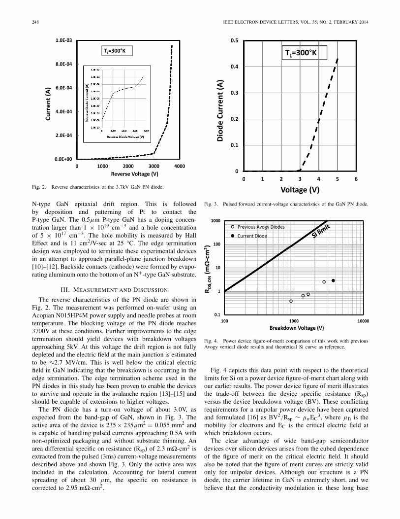
Fig. 2. Reverse characteristics of the 3.7kV GaN PN diode.
N-type GaN epitaxial drift region. This is followedby deposition and patterning of Pt to contact theP-type GaN. The 0.5μm P-type GaN has a doping concen-tration larger than 1 × 1019 cm−3 and a hole concentrationof 5 × 1017 cm−3. The hole mobility is measured by HallEffect and is 11 cm2/V-sec at 25 °C. The edge terminationdesign was employed to terminate these experimental devicesin an attempt to approach parallel-plane junction breakdown[10]–[12]. Backside contacts (cathode) were formed by evapo-rating aluminum onto the bottom of an N+-type GaN substrate.
III. MEASUREMENT AND DISCUSSION
The reverse characteristics of the PN diode are shown inFig. 2. The measurement was performed on-wafer using anAcopian N015HP4M power supply and needle probes at roomtemperature. The blocking voltage of the PN diode reaches3700V at these conditions. Further improvements to the edgetermination should yield devices with breakdown voltagesapproaching 5kV. At this voltage the drift region is not fullydepleted and the electric field at the main junction is estimatedto be ≈2.7 MV/cm. This is well below the critical electricfield in GaN indicating that the breakdown is occurring in theedge termination. The edge termination scheme used in thePN diodes in this study has been proven to enable the devicesto survive and operate in the avalanche region [13]–[15] andshould be capable of extensions to higher voltages.
The PN diode has a turn-on voltage of about 3.0V, asexpected from the band-gap of GaN, shown in Fig. 3. Theactive area of the device is 235 × 235μm2 = 0.055 mm2 andis capable of handling pulsed currents approaching 0.5A withnon-optimized packaging and without substrate thinning. Anarea differential specific on resistance (Rsp) of 2.3 m�-cm2 isextracted from the pulsed (3ms) current-voltage measurementsdescribed above and shown Fig. 3. Only the active area wasincluded in the calculation. Accounting for lateral currentspreading of about 30 μm, the specific on resistance iscorrected to 2.95 m�-cm2.
Fig. 3. Pulsed forward current-voltage characteristics of the GaN PN diode.
Fig. 4. Power device figure-of-merit comparison of this work with previousAvogy vertical diode results and theoretical Si curve as reference.
Fig. 4 depicts this data point with respect to the theoreticallimits for Si on a power device figure-of-merit chart along withour earlier results. The power device figure of merit illustratesthe trade-off between the device specific resistance (Rsp)versus the device breakdown voltage (BV). These conflictingrequirements for a unipolar power device have been capturedand formulated [16] as BV2/Rsp ∼ μnEC
3, where μn is themobility for electrons and EC is the critical electric field atwhich breakdown occurs.
The clear advantage of wide band-gap semiconductordevices over silicon devices arises from the cubed dependenceof the figure of merit on the critical electric field. It shouldalso be noted that the figure of merit curves are strictly validonly for unipolar devices. Although our structure is a PNdiode, the carrier lifetime in GaN is extremely short, and webelieve that the conductivity modulation in these long base

KIZILYALLI et al.: 3.7 kV VERTICAL GaN PN DIODES 249
diodes is negligible. It should also be noted that the increasein the reverse leakage current above 1000V (Fig. 2) is aconcern for practical power device applications. The sourceof the increase in reverse diode current is associated withthe epitaxial growth of thick device layers (> 20μm) and thestarting substrate material quality. The topic of carrier lifetimesin low defect density GaN along with the impact of substratequality on reverse diode characteristics will be discussed infuture publications
IV. CONCLUSION
Vertical architectures should substantially reduce cost andincrease current densities in GaN devices. Vertical GaN PNdiodes discussed here show breakdown voltages of 3.7 kV,area differential specific on-resistance of 2.95 m�-cm2, and acurrent density of 1kA/cm2.
ACKNOWLEDGMENT
Contributions of B. Alvarez, M. Raj, and P. Bui-Quangare gratefully acknowledged. The authors thank the Office ofNaval Research and Dr. Daniel Green for their support.
REFERENCES
[1] N. Mohan, Power Electronic: A First Course. New York, NY, USA:Wiley, 2012.
[2] J. Palmour, J. Zhang, M. K. Das, et al., “SiC power devices for smartgrid systems,” in Proc. IEEE Int. Conf. Power Electron., Jun. 2010,pp. 1006–1013.
[3] J. W. Johnson, A. Zhang, W. Luo, et al., “Breakdown voltage andreverse recovery characteristics of free-standing GaN Schottky rec-tifiers,” IEEE Trans. Electron Devices, vol. 49, no. 1, pp. 32–36,Jan. 2002.
[4] Y. Uemoto, D. Shibata, M. Yanagihara, et al., “8300 V blocking voltageAlGaN/GaN power HFET with thick poly-AlN passivation,” in Proc.IEEE IEDM, Dec. 2007, pp. 861–864.
[5] Y. Dora, A. Chakraborty, L. McCarthy, et al., “High breakdown voltageachieved on AlGaN/GaN HEMTs with integrated slant field plates,”IEEE Electron Device Lett., vol. 27, no. 9, pp. 713–715, Sep. 2006.
[6] Y. Hatakeyama, K. Nomoto, N. Kaneda, et al., “Over 3.0 GW/cm2
figure-of-merit GaN p-n junction diodes on free-standing GaN sub-strates,” IEEE Electron Device Lett., vol. 32, no. 12, pp. 1674–1676,Dec. 2011.
[7] Y. Saitoh, K. Sumiyoshi, M. Okada, et al., “Extremely low on-resistanceand high breakdown voltage observed in vertical GaN Schottky barrierdiodes with high-mobility drift layers on low-dislocation-density gansubstrates,” Appl. Phys. Exp., vol. 3, pp. 081001-1–081001-3, Jul. 2010.
[8] B. Lu and T. Palacios, “High breakdown (>1500V) AlGaN/GaN HEMTsby substrate transfer technology,” IEEE Electron Device Lett., vol. 31,no. 9, pp. 951–953, Sep. 2010.
[9] C. Mion, J. Muth, E. Preble, et al., “Accurate dependence of galliumnitride thermal conductivity on dislocation density,” Appl. Phys. Lett.,vol. 89, pp. 092123-1–092123-3, Sep. 2006.
[10] J. Laroche, F. Ren, K. Baik, et al., “Design of edge termination forGaN power Schottky diodes,” J. Electrochem. Mater., vol. 34, no. 4,pp. 370–374, 2005.
[11] A. Bolotnikov, P. Muzykov, Q. Zhang, et al., “Junction terminationextension implementing drive-in diffusion of boron for high-voltage SiCdevices,” IEEE Trans. Electron Devices, vol. 57, no. 8, pp. 1930–1935,Aug. 2010.
[12] A. M. Ozbek and B. J. Baliga, “Planar nearly ideal edge-terminationtechnique for GaN devices,” IEEE Electron Device Lett., vol. 32, no. 3,pp. 300–302, Mar. 2011.
[13] H. Nie, A. Edwards, D. Bour, et al., “Vertical power devices inbulk GaN for 600–1700V applications,” in Proc. GOMAC Tech, 2013,pp. 265–268.
[14] I. C. Kizilyalli, A. Edwards, H. Nie, et al., “High voltage vertical GaNp-n diodes with avalanche capability,” IEEE Trans. Electron Devices,vol. 60, no. 10, pp. 3067–3070, Oct. 2013.
[15] D. Disney, H. Nie, A. Edwards, et al., “Vertical power diodes in bulkGaN,” in Proc. ISPSD, 2013, pp. 59–62.
[16] K. Shenai, R. Scott, and B. Baliga, “Optimum semiconductors forhigh-power electronics,” IEEE Trans. Electron Devices, vol. 36, no. 9,pp. 1811–1823, Sep. 1989.