hong kong university of science and technology - 728 ieee … · 2018-05-17 · 728 ieee electron...
TRANSCRIPT
728 IEEE ELECTRON DEVICE LETTERS, VOL. 37, NO. 6, JUNE 2016
Elevated-Metal–Metal-Oxide Thin-Film Transistor:Technology and Characteristics
Lei Lu, Jiapeng Li, Zhuoqun Feng, Hoi Sing Kwok, Fellow, IEEE, and Man Wong, Senior Member, IEEE
Abstract— A new device architecture, dubbed elevated-metal–metal-oxide (EMMO) thin-film transistor (TFT), is presentlyproposed. During a heat-treatment process in oxygen, conductivesource and drain regions spontaneously populated by donordefects are formed, while the defects in the channel regionare simultaneously passivated. Compared with that of the con-ventional back-channel-etched TFT, this architecture inherentlyaccommodates an etch-stop/passivation layer without increasingthe mask count. EMMO TFT demonstrated using indium–gallium–zinc oxide as an active layer exhibited good performancemetrics: a peak field-effect mobility of ∼14 cm2/Vs, a steepestpseudo-subthreshold slope of ∼120 mV/decade, a leakage currentlower than ∼10−14 A, an on/off-current ratio above ∼1010, andstability against environmental and electrical stress.
Index Terms— Indium-gallium-zinc oxide (IGZO), thin-filmtransistor, elevated metal, back-channel etched, mask-count.
I. INTRODUCTION
DUE to their superior attributes, such as transparency,low off-current (Ioff ) and reasonably high field-effect
mobility (μFE), metal-oxide (MO) thin-film transistors (TFTs)are being deployed to replace their silicon counterparts inthe backplanes of a new generation of flat-panel displays [1].Among a range of material candidates, zinc oxide (ZnO) andits variant, indium-gallium-zinc oxide (IGZO) have hithertobeen the most commonly studied.
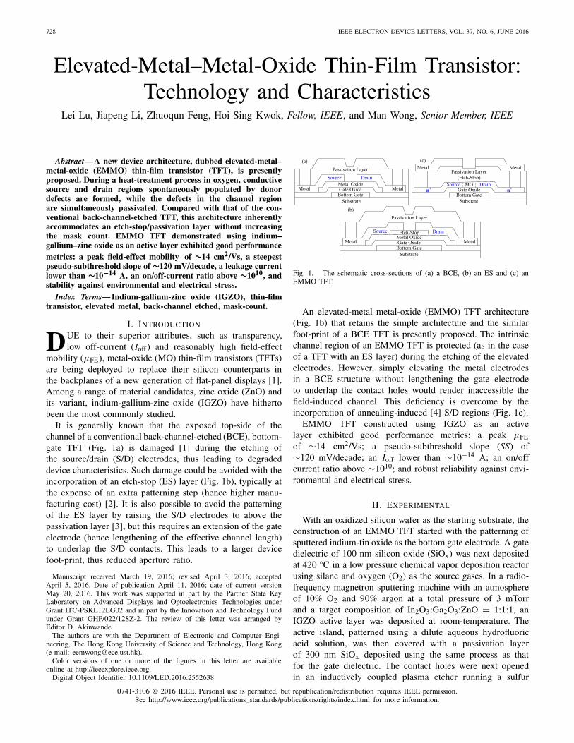
It is generally known that the exposed top-side of thechannel of a conventional back-channel-etched (BCE), bottom-gate TFT (Fig. 1a) is damaged [1] during the etching ofthe source/drain (S/D) electrodes, thus leading to degradeddevice characteristics. Such damage could be avoided with theincorporation of an etch-stop (ES) layer (Fig. 1b), typically atthe expense of an extra patterning step (hence higher manu-facturing cost) [2]. It is also possible to avoid the patterningof the ES layer by raising the S/D electrodes to above thepassivation layer [3], but this requires an extension of the gateelectrode (hence lengthening of the effective channel length)to underlap the S/D contacts. This leads to a larger devicefoot-print, thus reduced aperture ratio.
Manuscript received March 19, 2016; revised April 3, 2016; acceptedApril 5, 2016. Date of publication April 11, 2016; date of current versionMay 20, 2016. This work was supported in part by the Partner State KeyLaboratory on Advanced Displays and Optoelectronics Technologies underGrant ITC-PSKL12EG02 and in part by the Innovation and Technology Fundunder Grant GHP/022/12SZ-2. The review of this letter was arranged byEditor D. Akinwande.
The authors are with the Department of Electronic and Computer Engi-neering, The Hong Kong University of Science and Technology, Hong Kong(e-mail: [email protected]).
Color versions of one or more of the figures in this letter are availableonline at http://ieeexplore.ieee.org.
Digital Object Identifier 10.1109/LED.2016.2552638
Fig. 1. The schematic cross-sections of (a) a BCE, (b) an ES and (c) anEMMO TFT.
An elevated-metal metal-oxide (EMMO) TFT architecture(Fig. 1b) that retains the simple architecture and the similarfoot-print of a BCE TFT is presently proposed. The intrinsicchannel region of an EMMO TFT is protected (as in the caseof a TFT with an ES layer) during the etching of the elevatedelectrodes. However, simply elevating the metal electrodesin a BCE structure without lengthening the gate electrodeto underlap the contact holes would render inaccessible thefield-induced channel. This deficiency is overcome by theincorporation of annealing-induced [4] S/D regions (Fig. 1c).
EMMO TFT constructed using IGZO as an activelayer exhibited good performance metrics: a peak μFEof ∼14 cm2/Vs; a pseudo-subthreshold slope (SS) of∼120 mV/decade; an Ioff lower than ∼10−14 A; an on/offcurrent ratio above ∼1010; and robust reliability against envi-ronmental and electrical stress.
II. EXPERIMENTAL
With an oxidized silicon wafer as the starting substrate, theconstruction of an EMMO TFT started with the patterning ofsputtered indium-tin oxide as the bottom gate electrode. A gatedielectric of 100 nm silicon oxide (SiOx) was next depositedat 420 °C in a low pressure chemical vapor deposition reactorusing silane and oxygen (O2) as the source gases. In a radio-frequency magnetron sputtering machine with an atmosphereof 10% O2 and 90% argon at a total pressure of 3 mTorrand a target composition of In2O3:Ga2O3:ZnO = 1:1:1, anIGZO active layer was deposited at room-temperature. Theactive island, patterned using a dilute aqueous hydrofluoricacid solution, was then covered with a passivation layerof 300 nm SiOx deposited using the same process as thatfor the gate dielectric. The contact holes were next openedin an inductively coupled plasma etcher running a sulfur
0741-3106 © 2016 IEEE. Personal use is permitted, but republication/redistribution requires IEEE permission.See http://www.ieee.org/publications_standards/publications/rights/index.html for more information.

LU et al.: EMMO TFT: TECHNOLOGY AND CHARACTERISTICS 729
Fig. 2. The transfer characteristics of an EMMO TFT with channellength/width of 42 μm/100 μm. Solid and hollow symbols denote, respec-tively, forward and reverse Vg sweeps.
hexafluoride chemistry. Finally, with the IGZO intrinsic chan-nel region protected by the SiOx passivation (thus equivalentto an inherent ES) layer, a sputtered molybdenum/aluminum(Mo/Al) bilayer was patterned to form the S/D electrodes witha 4 μm overlap with the gate electrode.
As shown in the Inset of Figure 2, when IGZO covered withgas-permeable SiOx was annealed in an atmosphere cyclicallyswitched between nitrogen (N2) and O2, a correspondingchange in its resistivity (ρ) from low to high was observed.When a gas-impermeable layer of Al was placed on top of theSiOx, the ρ stayed low regardless of the annealing atmosphere.Similar behavior has been comprehensively reported [4], [5]with silicon nitride as an impermeable cover.
An EMMO TFT is realized by combining gas-impermeableelectrodes with a heat-treatment in O2. Shielded from theoxidizing atmosphere, the active areas covered under theelectrodes were converted to annealing-induced conductiveS/D regions [4] to access the field-induced channel of the TFT.Exposed to the oxidizing atmosphere through the perme-able SiOx layer, the active channel area not covered by theelectrodes remained intrinsic – due to the passivation andsuppressed generation [4], [5] of donor-defects.
A series of drain current (Id) vs. gate voltage (Vg) transfercharacteristics at different drain voltage (Vd) of an EMMOTFT heat-treated at 400 °C in O2 for 2 hours were measuredusing an Agilent 4155C Semiconductor Parameter Analyzerand shown in Figure 2.
A low Ioff was obtained, below the ∼10−14 A detectionlimit of the Analyzer. For conventionally processed IGZOTFTs, both the Ioff and the hysteresis could be degraded by theincorporation during the fabrication process of unintentionalexternal impurities such as hydrogen [6] or the generationof defects such as oxygen vacancies (VO) [7]. Such processcould include the back-channel etch when patterning the metalelectrodes [8]; the plasma bombardment when depositing theES and passivation layers [9] and other improperly designedthermal processes [5], [10]. On the contrary, the oxidizingannealing of the EMMO TFT performed towards the end ofits fabrication process − in fact after the formation of the
Fig. 3. The output characteristics at various Vg for an EMMO TFT. Shownin the Inset are the output characteristics at low Vd.
metal electrodes − prevented the formation of donor-defects(thus ensuring a highly intrinsic ρ in the active channel regionof the TFT, hence a low Ioff [10]).
Hysteresis was clearly negligible in the transfer charac-teristics. This resulted from not only the good quality ofthe channel region, but also the elimination [11] of residualhydrogen [6], [10], [12]. From the transfer characteristicmeasured at a Vd of 10V, a steepest SS of ∼120 mV/decade,a saturation threshold voltage of ∼0.4 V extracted from thedependence of I 0.5
d on Vg and a peak μFE of ∼14 cm2/Vsextracted from the maximum ∂ I 0.5
d /∂Vg are obtained. Thelow Ioff , combined with the reasonably high μFE, leads toa high on-off current ratio of better than ∼1010.
Id vs. Vd output characteristics (Fig. 3) were also measuredat various Vg. The nice linear dependence of Id on Vd shownin the Inset is a reflection of the good ohmic contact betweenthe highly conductive annealing-induced S/D regions and theMo/Al metal electrodes.
In addition to the good device characteristics, reliabilityagainst environmental and electrical stress has also been stud-ied. Various approaches for reliability enhancement have beenproposed: by improving the passivation layer [9], adjustingthe composition and oxygen content of the MO [13], modify-ing the TFT architecture [14], and designing proper processtechnologies [15], [16]. Shown in Figure 4 is a demonstrationof the effectiveness of the 300 nm SiOx passivation layeragainst environmental stress. The measured transfer charac-teristics hardly changed after storage in 90% humidity at80 °C for 10 hours. The reliability of EMMO TFT againstpositive/negative bias stress (PBS/NBS) was also investigated,with grounded S/D and respective Vg of +20 and −20 V.The transfer characteristics hardly changed throughout the30,000 second stress, as is evident from their time evolutionin Insets (a) and (b) of Figure 4.
The PBS/NBS-induced degradation in an MO TFT is com-monly ascribed to defects in the MO, such as VO [15], [16].Suppressing the population of VO is thus an effective methodof enhancing the reliability of a TFT [15]–[17]. One approachis heat-treatment in an oxidizing atmosphere, such as watervapor [15] and air [16]. Consistent with the annealing in anoxidizing atmosphere used in the realization of an EMMO

730 IEEE ELECTRON DEVICE LETTERS, VOL. 37, NO. 6, JUNE 2016
Fig. 4. Comparison of the transfer characteristics of EMMO TFT beforeand after environmental stress in 90% humidity at 80 °C for 10 hours. Shownin the Insets are the time evolutions of the transfer characteristics of EMMOTFT under (a) PBS and (b) NBS.
TFT, it is not surprising that good reliability against bothenvironmental and electrical stress is obtained.
III. CONCLUSION
A new bottom-gate metal-oxide transistor architecture,dubbed EMMO TFT, is proposed and demonstrated. Themulti-fold superiority of this device structure includes: provi-sion of a spontaneous ES layer without an additional maskingstep; the ES layer also functioning as a passivation layeragainst environmental exposure; an oxidation-last annealingheat-treatment ensuring good quality of the intrinsic channelregion – thus leading to good device characteristics andreliability.
ACKNOWLEDGMENT
We would like to thank the staff of the NanoelectronicsFabrication Facility (NFF) of the Hong Kong Universityof Science and Technology for their assistance in devicefabrication.
REFERENCES
[1] E. Fortunato, P. Barquinha, and R. Martins, “Oxide semi-conductor thin-film transistors: A review of recent advances,”Adv. Mater., vol. 24, no. 22, pp. 2945–2986, Jun. 2012,doi: 10.1002/adma.201103228.
[2] S. Yamazaki, T. Hirohashi, M. Takahashi, S. Adachi, M. Tsubuku,J. Koezuka, K. Okazaki, Y. Kanzaki, H. Matsukizono, S. Kaneko,S. Mori, and T. Matsuo, “Back-channel-etched thin-film transistor usingc-axis-aligned crystal In–Ga–Zn oxide,” J. Soc. Inf. Display, vol. 22,no. 1, pp. 55–67, Jan. 2014, doi: 10.1002/jsid.211.
[3] T. Hirao, M. Furuta, T. Hiramatsu, T. Matsuda, C. Li, H. Furuta,H. Hokari, M. Yoshida, H. Ishii, and M. Kakegawa, “Bottom-gatezinc oxide thin-film transistors (ZnO TFTs) for AM-LCDs,” IEEETrans. Electron Devices, vol. 55, no. 11, pp. 3136–3142, Nov. 2008,doi: 10.1109/TED.2008.2003330.
[4] L. Lu and M. Wong, “A bottom-gate indium–gallium–zinc oxide thin-film transistor with an inherent etch-stop and annealing-induced sourceand drain regions,” IEEE Trans. Electron Devices, vol. 62, no. 2,pp. 574–579, Feb. 2015, doi: 10.1109/TED.2014.2375194.
[5] L. Lu and M. Wong, “The resistivity of zinc oxide under differentannealing configurations and its impact on the leakage characteristics ofzinc oxide thin-film transistors,” IEEE Trans. Electron Devices, vol. 61,no. 4, pp. 1077–1084, Apr. 2014, doi: 10.1109/TED.2014.2302431.
[6] T. Toda, D. Wang, J. Jiang, M. P. Hung, and M. Furuta, “Quantitativeanalysis of the effect of hydrogen diffusion from silicon oxide etch-stopper layer into amorphous In–Ga–Zn–O on thin-film transistor,” IEEETrans. Electron Devices, vol. 61, no. 11, pp. 3762–3767, Nov. 2014,doi: 10.1109/TED.2014.2359739.
[7] T. Kamiya, K. Nomura, and H. Hosono, “Origins of high mobility andlow operation voltage of amorphous oxide TFTs: Electronic structure,electron transport, defects and doping,” J. Display Technol., vol. 5,no. 12, pp. 468–483, Dec. 2009, doi: 10.1109/JDT.2009.2034559.
[8] S. H. Ryu, Y. C. Park, M. Mativenga, D. H. Kang, and J. Jang,“Amorphous-InGaZnO4 thin-film transistors with damage-free backchannel wet-etch process,” ECS Solid State Lett., vol. 1, no. 2,pp. Q17–Q19, Jul. 2012, doi: 10.1149/2.004202ssl.
[9] M. D. H. Chowdhury, M. Mativenga, J. G. Um, R. K. Mruthyunjaya,G. N. Heiler, T. J. Tredwell, and J. Jang, “Effect of SiO2and SiO2/SiNx passivation on the stability of amorphous indium–gallium zinc-oxide thin-film transistors under high humidity,” IEEETrans. Electron Devices, vol. 62, no. 3, pp. 869–874, Mar. 2015,doi: 10.1109/TED.2015.2392763.
[10] L. Lu, J. Li, and M. Wong, “A comparative study on theeffects of annealing on the characteristics of zinc oxide thin-film transistors with gate-stacks of different gas-permeability,” IEEEElectron Device Lett., vol. 35, no. 8, pp. 841–843, Aug. 2014,doi: 10.1109/LED.2014.2326960.
[11] L. Lu, J. Li, and M. Wong, “Thermally induced variation of the turn-ON voltage of an indium–gallium–zinc oxide thin-film transistor,” IEEETrans. Electron Devices, vol. 62, no. 11, pp. 3703–3708, Nov. 2015,doi: 10.1109/TED.2015.2478839.
[12] M. Fakhri, H. Johann, P. Görrn, and T. Riedl, “Water as origin of hystere-sis in zinc tin oxide thin-film transistors,” ACS Appl. Mater. Interfaces,vol. 4, no. 9, pp. 4453–4456, Sep. 2012, doi: 10.1021/am301308y.
[13] L.-C. Liu, J.-S. Chen, and J.-S. Jeng, “Role of oxygen vacancies on thebias illumination stress stability of solution-processed zinc tin oxide thinfilm transistors,” Appl. Phys. Lett., vol. 105, no. 2, p. 023509, Jul. 2014,doi: 10.1063/1.4890579.
[14] Y.-C. Chen, T.-C. Chang, H.-W. Li, T.-Y. Hsieh, T.-C. Chen, C.-P. Wu,C.-H. Chou, W.-C. Chung, J.-F. Chang, and Y.-H. Tai, “The suppressednegative bias illumination-induced instability in In–Ga–Zn–O thin filmtransistors with fringe field structure,” Appl. Phys. Lett., vol. 101, no. 22,p. 223502, 2012, doi: 10.1063/1.4767996.
[15] Y. S. Rim, W. Jeong, B. D. Ahn, and H. J. Kim, “Defect reductionin photon-accelerated negative bias instability of InGaZnO thin-filmtransistors by high-pressure water vapor annealing,” Appl. Phys. Lett.,vol. 102, no. 14, p. 143503, 2013, doi: 10.1063/1.4801436.
[16] X. Li, E. Xin, L. Chen, J. Shi, C. Li, and J. Zhang, “Depen-dence of annealing on stability of transparent amorphous InGaZnOthin film transistor,” Mater. Sci. Semicond. Process., vol. 16, no. 5,pp. 1292–1296, Oct. 2013, doi: 10.1016/j.mssp.2013.02.013.
[17] T. Bradley, S. Iyer, R. Alston, W. Collis, J. Lewis, G. Cunningham, andE. Forsythe, “The effects of deposition conditions and annealing temper-ature on the performance of gallium tin zinc oxide thin film transistors,”Proc. SPIE, vol. 8626, p. 862615, Mar. 2013, doi: 10.1117/12.2013277.