high speed design considerations - altium
TRANSCRIPT

High Speed Design Considerations
HIGH SPEED DESIGN CONSIDERATIONS
www.altium.com
HIGH SPEED DESIGN CONSIDERATIONS
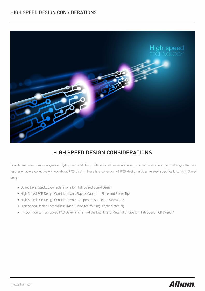
Boards are never simple anymore. High speed and the proliferation of materials have provided several unique challenges that are
testing what we collectively know about PCB design. Here is a collection of PCB design articles related specifically to High Speed
design:
Board Layer Stackup Considerations for High Speed Board Design
High Speed PCB Design Considerations: Bypass Capacitor Place and Route Tips
High Speed PCB Design Considerations: Component Shape Considerations
High-Speed Design Techniques: Trace Tuning for Routing Length Matching
Introduction to High Speed PCB Designing: Is FR-4 the Best Board Material Choice for High Speed PCB Design?
HIGH SPEED DESIGN CONSIDERATIONS
www.altium.com
BOARD LAYER STACKUP CONSIDERATIONS FOR HIGH SPEED BOARD
DESIGN
I’ve been designing boards for a long time; however when I began my career, the boards I designs were pretty simple. Most of them
were small low speed designs with very few restrictions on them. Test boards and control panels, I cannot tell you how many simple
2 and 4 layer boards I have designed in my career. That being said, as my skills increased, so did the complexity of the boards that I
designed. A particular high point for me was when I began working on dense multi-layer high speed designs.
High speed PCB designs have tighter signal integrity requirements, and constructing your board for them becomes part of the
overall signal integrity equation. Not only is the selection of board materials important for impedance, dissipation and other signal
characteristics, but the order and number of layers of those materials play a vital role as well.

HIGH SPEED DESIGN CONSIDERATIONS
www.altium.com
Plan out your designs and routing.
STACKUP REQUIREMENTS FOR HIGH SPEED ROUTING
High speed signals are most often routed using either microstrip or stripline methodologies. These methods are designed so that a
high speed signal running through a routed trace will have the correct physical structure for its return path. The physical structure
requirements of these routing methods will have a great impact on your board stackup decisions.
Microstrip is the simpler methodology of the two. It has a transmission line, which is a routed trace on an external layer of the board,
that is separated from its referenced ground plane by a layer of dielectric material. Alternatively, stripline has a referenced ground
plane both above and below the transmission line. The transmission line is a routed trace on an internal signal layer which is
embedded in dielectric material balanced between the two planes.
When planning your board stackup for a high speed design, you will need to take into account these routing methods. When routing
microstrip, your board stackup will have to include a ground plane next to the external routing layers of the board. When routing
stripline your board stackup will have to include ground planes on both sides of an internal signal layer where the high speed routing
is being done. There are also other types of stripline which you may need to consider as well. For example, dual stripline requires
that you surround two adjacent internal signal layers with ground planes.
HIGH SPEED DESIGN CONSIDERATIONS
www.altium.com
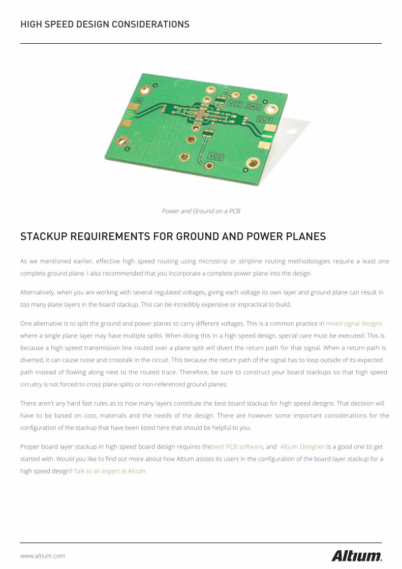
Power and Ground on a PCB
STACKUP REQUIREMENTS FOR GROUND AND POWER PLANES
As we mentioned earlier, effective high speed routing using microstrip or stripline routing methodologies require a least one
complete ground plane. I also recommended that you incorporate a complete power plane into the design.
Alternatively, when you are working with several regulated voltages, giving each voltage its own layer and ground plane can result in
too many plane layers in the board stackup. This can be incredibly expensive or impractical to build.
One alternative is to split the ground and power planes to carry different voltages. This is a common practice in mixed signal designs
where a single plane layer may have multiple splits. When doing this In a high speed design, special care must be executed. This is
because a high speed transmission line routed over a plane split will divert the return path for that signal. When a return path is
diverted, it can cause noise and crosstalk in the circuit. This because the return path of the signal has to loop outside of its expected
path instead of flowing along next to the routed trace. Therefore, be sure to construct your board stackups so that high speed
circuitry is not forced to cross plane splits or non-referenced ground planes.
There aren’t any hard fast rules as to how many layers constitute the best board stackup for high speed designs. That decision will
have to be based on cost, materials and the needs of the design. There are however some important considerations for the
configuration of the stackup that have been listed here that should be helpful to you.
Proper board layer stackup in high speed board design requires the best PCB software, and Altium Designer is a good one to get
started with. Would you like to find out more about how Altium assists its users in the configuration of the board layer stackup for a
high speed design? Talk to an expert at Altium.

HIGH SPEED DESIGN CONSIDERATIONS
www.altium.com
HIGH SPEED PCB DESIGN CONSIDERATIONS: BYPASS CAPACITOR PLACE
AND ROUTE TIPS
Many years ago, the majority of the board designs that I was involved with were simple digital designs. Placing and routing bypass
capacitors in those designs was very easy, and often the circuitry was slow enough that capacitors were not needed. Most of the
time we considered bypass capacitor placement and routing as more of an afterthought than as a primary design consideration. I
remember how some of the engineers even instructed me to “sprinkle” bypass capacitors here and there as if they were little more
than candied decorations on a cake. There didn’t seem to be much concern about how many to use, where they should be placed,
or how they should be connected.
Later on, as designs grew in complexity and speed, the need for designing a more refined power distribution network (PDN) on the
circuit board increased as well. Now with the signal integrity requirements of a high speed design, a precisely designed PDN has
become imperative for the best performance of the circuit board.
Let’s look at what some of the bypass capacitor requirements are in the PDN of a high speed design, and what kind of placement
and routing strategies will best help you.
HIGH SPEED DESIGN CONSIDERATIONS
www.altium.com
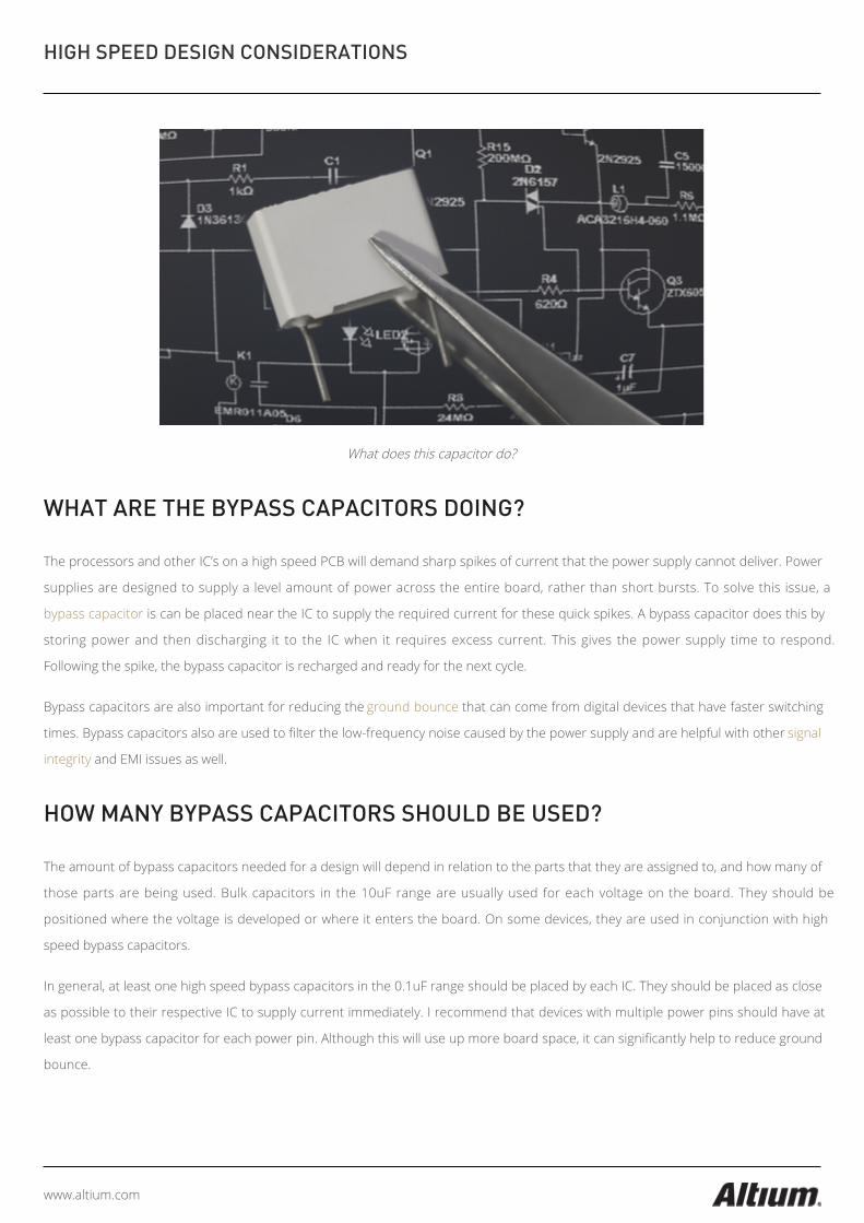
What does this capacitor do?
WHAT ARE THE BYPASS CAPACITORS DOING?
The processors and other IC’s on a high speed PCB will demand sharp spikes of current that the power supply cannot deliver. Power
supplies are designed to supply a level amount of power across the entire board, rather than short bursts. To solve this issue, a
bypass capacitor is can be placed near the IC to supply the required current for these quick spikes. A bypass capacitor does this by
storing power and then discharging it to the IC when it requires excess current. This gives the power supply time to respond.
Following the spike, the bypass capacitor is recharged and ready for the next cycle.
Bypass capacitors are also important for reducing the ground bounce that can come from digital devices that have faster switching
times. Bypass capacitors also are used to filter the low-frequency noise caused by the power supply and are helpful with other signal
integrity and EMI issues as well.
HOW MANY BYPASS CAPACITORS SHOULD BE USED?
The amount of bypass capacitors needed for a design will depend in relation to the parts that they are assigned to, and how many of
those parts are being used. Bulk capacitors in the 10uF range are usually used for each voltage on the board. They should be
positioned where the voltage is developed or where it enters the board. On some devices, they are used in conjunction with high
speed bypass capacitors.
In general, at least one high speed bypass capacitors in the 0.1uF range should be placed by each IC. They should be placed as close
as possible to their respective IC to supply current immediately. I recommend that devices with multiple power pins should have at
least one bypass capacitor for each power pin. Although this will use up more board space, it can significantly help to reduce ground
bounce.

HIGH SPEED DESIGN CONSIDERATIONS
www.altium.com
Capacitors and other parts at work on a PCB
BYPASS CAPACITOR PLACEMENT AND ROUTING BEST PRACTICES
As I mentioned earlier, you should place your bypass capacitors as close as possible to the device that they are assigned to. This can
be underneath the device on the opposite side of the board, or just off the pins that the bypass capacitor is connected to on the
same side of the board.
For circuits requiring multiple bypass capacitors placed near the power pin of a specific device, the capacitors should be placed next
to that pin in ascending order of value. For instance, if both a .01uF and a 10uF capacitor are specified for a specific device, place the
.01uF closest to the device with the 10uF outboard of that. In this way, the larger bulk capacitor will recharge the high-frequency
capacitor that is closest to the device pin.
When routing a bypass capacitor, you should start from the power or ground pin of the device and go directly to the capacitor pin.
From there the route can continue on to a via connecting it to the power or ground plane. You should also use as short and wide
traces as possible to connect the bypass capacitor, and use as many vias to connect to the power or ground plane as possible.
The placement and routing of your bypass capacitors for the best possible power distribution network is an important part of your
high speed PCB design. The tips that have been discussed here will give you a good start, and there are other resources available to
you as well. PCB software, like Altium Designer, has DC analysis tools, like their PDN Analyzer. These let you analyze and resolve
power distribution network issues during the layout of the PCB before you build an actual board.
Would you like to find out more about how Altium can help with the layout of your high speed PCB design? Talk to an expert at
Altium.

HIGH SPEED DESIGN CONSIDERATIONS
www.altium.com
HIGH SPEED PCB DESIGN CONSIDERATIONS: COMPONENT SHAPE
CONSIDERATIONS
When starting a high speed PCB design, there’s a lot that must be considered before the design ever gets into layout. Schematic
organization, board materials & layer configuration, critical component placement, and how high speed signals are to be routed are
all aspects of high speed design that need to be planned for.
Often there is one area that doesn’t get as much consideration as everything else, and that is the component footprint shapes. The
components used in a high speed design aren’t physically different than what would be used in a conventional design. However,
there are some subtle changes that can be made to pad and component footprint shapes that will help your efforts in creating a
high speed PCB design.
PAD SHAPES FOR HIGH SPEED PCB DESIGN
When evaluating footprint shapes for use in high speed design, the first item to consider is the size of the footprint pad shapes.
Sometimes referred to as landing pads, these shapes are the bare metal pads that the component pins will be soldered to on the
finished PCB. Usually, one or two pad shapes are duplicated to create an entire component footprint shape.
Traditionally PCB pads are larger than the pins by approximately 30%. These sizes are calculated for optimum manufacturing in
order to avoid problems like “tombstoning” where discrete surface mount parts like capacitors and resistors will flip up on one side.
These optimum sizes also allow for manual rework with a handheld soldering iron and visual inspection of a solder joint. However,
HIGH SPEED DESIGN CONSIDERATIONS
www.altium.com
for a high speed design, the extra metal can increase parasitic capacitance and increase the connection length between critical
components.
To help the high speed needs of the circuit, the pad size should be reduced. Instead of oversizing the pad 30% from the actual pin
size, a smaller percentage such as 5% is more beneficial. The smaller pad size helps reduce possible parasitic capacitance. As well,
connection lengths can be mitigated by decreasing the spacing between components. This practice is also appealing since it uses
less board space. Using smaller pad sizes does not reduce their mechanical strength since the contact area between the component
pins and the PCB remains the same. However, their trade-off is in the manufacturability of the board. Smaller pad sizes and tighter
spacing increases the manufacturing cost of the board. The design team will have to negotiate the high speed needs of the design
with the design for manufacturability needs of manufacturing prior to laying out the PCB.
Rounding the corners of the pad shapes is another enhancement that will benefit your high speed design. Rounded corners will
allow you to route traces closer to the pads which will decrease connection lengths and help to compact the size of the laid out
circuitry as well.
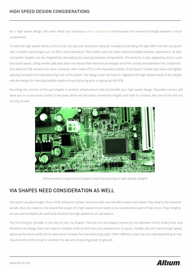
Enhancements to pad and via shapes could help spacing on high-density designs
VIA SHAPES NEED CONSIDERATION AS WELL
Via’s aren’t usually thought of as a PCB component shape, but since their size will affect board real estate, they need to be looked at
as well. Also, any metal on the board that is part of a high speed circuit needs to be considered as part of that circuit. Trace lengths,
via size and via depths all need to be factored into high speed circuit calculations.
The first thing to consider is the size of your via shapes. The size of a via shape is driven by the diameter of the drilled hole, and
therefore the design team will need to consider what via drill sizes are needed prior to layout. Smaller vias will improve high speed
signal performance while at the same time increase the manufacturing costs. Often different sized vias are used depending on the
requirements of the circuit or whether the vias are conducting power or ground.

HIGH SPEED DESIGN CONSIDERATIONS
www.altium.com
Once the via sizes have been decided, the next thing to look at is their placement in relationship to component pads. Conventionally
in non-high speed designs, the vias are pulled away from the component pad to maintain optimum pad to via spacing for
manufacturing purposes. The pad is then connected to the via with a trace. However, these connection lengths might be too long for
a high speed design.
To shorten the connection length the via can be placed closer to the pad, partially on the pad, or even completely within the pad.
Placing vias like this may require different CAD setups and DRC adjustments, or even the inclusion of a via shape within a pad shape.
It is also a good practice to use short wide traces to connect a decoupling capacitor pad to a via.
High speed design components should be evaluated for the best package for the circuit
COMPONENT SELECTION AND PLACEMENT
There are some component footprint options to consider as well. Sockets can have inductance associated with them. Therefore, it is
a good practice to eliminate or minimize the use of sockets in a high speed design. Selecting the correct package, and accompanying
component footprint, is also important. Some devices, like Op amps, are typically offered in different packages. One variation of an
Op-amp may allow shorter trace lengths in a circuit than another. Lastly, component footprint shapes may need to be adjusted for
thermal considerations. An excellent way to dissipate heat is to place power pads directly under IC footprint shapes that are
connected to an internal plane.
PCB footprint and pad shapes can help with the creation of your high speed PCB design. Even the smallest change could help you
tighten up the routing and decrease the connection lengths, or even reduce problems from parasitic inductance or high speed
thermal issues.
Would you like to know more about PCB design software? Talk to an expert at Altium.

HIGH SPEED DESIGN CONSIDERATIONS
www.altium.com
HIGH-SPEED DESIGN TECHNIQUES: TRACE TUNING FOR ROUTING
LENGTH MATCHING
The first time I heard someone talking about “tuning” their high-speed PCB design, the memory of my middle school band came to
mind. Back in those days, “tuning” meant taking kids who lacked experience and who used tired old instruments and trying to turn it
all into something that blended together. As you would expect, our first attempts at being in tune were not very successful. After
some work, though, we were able to stay in tune together, and we began to sound like a real band.
A band tunes up so that each instrument is in sync with the rest of the instruments in the band. When everyone plays a concert B-
flat, it should all sound like the same note. On the other hand, when a band is out of tune it can actually hurt to listen to the sound of
the different instruments fighting against each other.
Like a band, a high speed printed circuit board design also needs to be “tuned up.” There are high-speed nets that must have
specific lengths “tuned” to each other to function as intended. Let’s take a look at what trace tuning is on a PCB and discuss some
ideas on how to best accomplish it.
HIGH SPEED DESIGN CONSIDERATIONS
www.altium.com
WHAT IS TRACE TUNING?
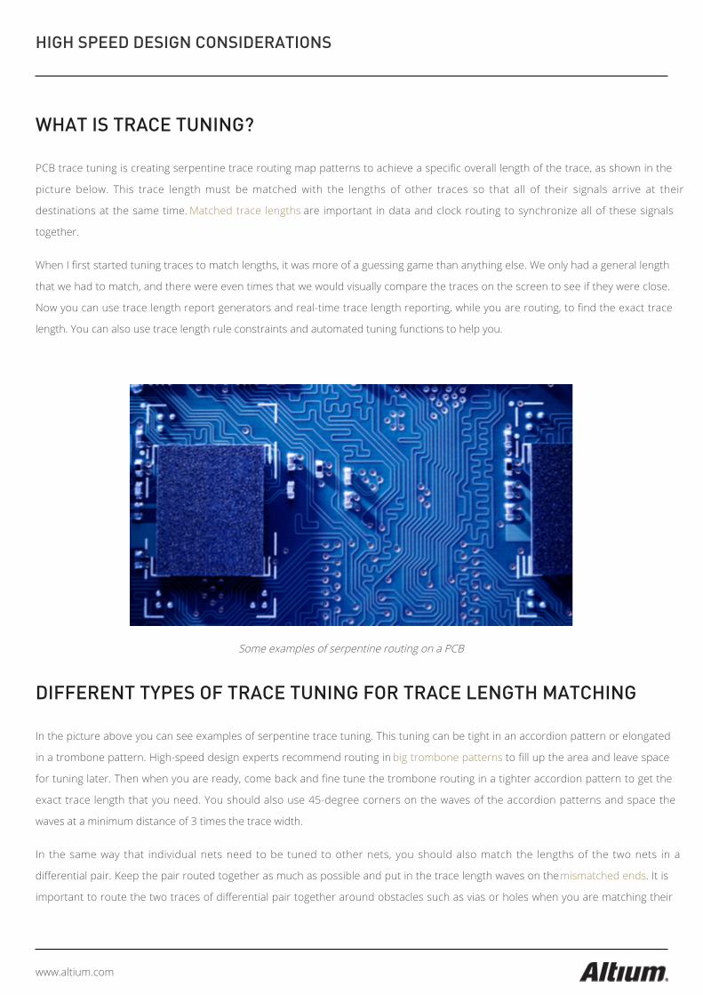
PCB trace tuning is creating serpentine trace routing map patterns to achieve a specific overall length of the trace, as shown in the
picture below. This trace length must be matched with the lengths of other traces so that all of their signals arrive at their
destinations at the same time. Matched trace lengths are important in data and clock routing to synchronize all of these signals
together.
When I first started tuning traces to match lengths, it was more of a guessing game than anything else. We only had a general length
that we had to match, and there were even times that we would visually compare the traces on the screen to see if they were close.
Now you can use trace length report generators and real-time trace length reporting, while you are routing, to find the exact trace
length. You can also use trace length rule constraints and automated tuning functions to help you.
Some examples of serpentine routing on a PCB
DIFFERENT TYPES OF TRACE TUNING FOR TRACE LENGTH MATCHING
In the picture above you can see examples of serpentine trace tuning. This tuning can be tight in an accordion pattern or elongated
in a trombone pattern. High-speed design experts recommend routing in big trombone patterns to fill up the area and leave space
for tuning later. Then when you are ready, come back and fine tune the trombone routing in a tighter accordion pattern to get the
exact trace length that you need. You should also use 45-degree corners on the waves of the accordion patterns and space the
waves at a minimum distance of 3 times the trace width.
In the same way that individual nets need to be tuned to other nets, you should also match the lengths of the two nets in a
differential pair. Keep the pair routed together as much as possible and put in the trace length waves on the mismatched ends. It is
important to route the two traces of differential pair together around obstacles such as vias or holes when you are matching their

HIGH SPEED DESIGN CONSIDERATIONS
www.altium.com
lengths. Don’t split the pair up while routing around these obstacles. Differential pairs will also need to be matched in length to other
differential pairs as well.
PCB trace routing
TRACE TUNING FUNCTIONALITY THAT WILL HELP YOU
There is a lot of functionality in PCB design tools that will help you with your routing and trace tuning. First, you can set up trace
length rules in the high-speed routing constraints. These rules will ensure that your routing is created at the correct lengths and
appropriately matched to other nets. You can also use processes that will automatically route the tuning patterns to the correct
lengths so that you don’t have to manually create the waves. These utilities provide the control you need to regulate the trace width
and the height and spacing of the accordion wave patterns. Finally, you can also use differential pair routers to match the lengths of
the two traces in the pair together.
PCB design software, like Altium Designer, has high-speed design functionality for routing and trace tuning built into it. This will help
you to route the high speed traces on your PCB to the correct lengths without having to guess their actual lengths. With this kind of
help, you can create a high-speed compliant design in less time and with greater confidence in its accuracy.
Would you like to find out more about how Altium can help you with your high-speed design needs? Talk to an expert at Altium.

HIGH SPEED DESIGN CONSIDERATIONS
www.altium.com
INTRODUCTION TO HIGH SPEED PCB DESIGNING: IS FR-4 THE BEST
BOARD MATERIAL CHOICE FOR HIGH SPEED PCB DESIGN?
We’ve all been there at one time or another when we’re tasked with a project that lies outside our comfort zone. For me, that day
came when my boss asked me to design a high speed board. While I considered myself to be a somewhat experienced circuit
designer, I knew that high speed PCB design has many restrictions that you do not normally encounter when you’re designing an
average circuit. Initially I invested time into making my schematics appropriate for high speed designs; however, once that was
complete I was completely focused on understanding whether I should use FR-4 or a more specialized material for my high speed
PCB. Before I get into what I’ve learned, it’s important to know what in this article I refer to “high speed” as anything greater than 50
MHz. These are the material considerations you should take note of when working in this frequency range.
High speed designs have tighter specifications on signal integrity than other designs. Although great care is taken in the routing of
high speed signals to satisfy these requirements, it must be understood that the board materials themselves are part of the overall
signal integrity equation. Board materials for high speed designs, therefore, need properties such as a dielectric constant with tight
tolerances to help control impedance. If impedance is allowed to vary across the design, then the high speed signals will begin to
reflect energy back as they move through their lines and the signal will be distorted. Also, a low dissipation factor to help maintain
signal integrity is desirable. Finally, thermal stability is another important trait to ensure that the dielectric properties will not
breakdown.

HIGH SPEED DESIGN CONSIDERATIONS
www.altium.com
FR-4: ITS STRENGTHS AND ITS WEAKNESSES
For as long as I’ve been designing printed circuit boards, FR-4 has been the standard material used for the fabrication of a PCB. Back
in the day as junior designers we even had the bad habit of referring to all boards as being “FR-4” whether they were constructed
with it or not. FR-4 is a Flame Retardant type 4 woven glass reinforced epoxy laminate. It is a very cost effective material that is both
an excellent electrical insulator and very sturdy in dry and humid conditions. It also has good fabrication properties making it an ideal
material for constructing a PCB.
The downside of FR-4 is that it has operating limitations when it comes to excessive power, voltage or heat. If you exceed its
operating limits, FR-4’s dielectric properties will break down. This means that the insulation of the material will decrease and it will
begin to conduct electricity instead. Another problem with FR-4 is maintaining stable impedance for high speed designs. This is
because the dielectric constant of FR-4 can vary across the length and width of the board. Also, the signal losses that are acceptable
in non-high speed designs will increase to undesirable levels in FR-4 boards as the speed of the design increases.
Let’s compare board materials
HOW SPECIFIC HIGH SPEED BOARD MATERIALS COMPARE WITH FR4
Dedicated high speed board materials such as Thermoset Hydrocarbon and PTFE laminates, will have better and more reliable
properties in higher frequency designs than FR-4. There some trade-offs, which we will discuss shortly, but first let’s look at some of
the advantages that high speed board design materials offer:
Decreased Signal Loss. As transmission line frequencies increase, signal loss becomes more of a problem. High speed design1.
board materials have a much lower dissipation factor than FR-4, with some of the materials, such as the nearly pure PTFE
laminates, being an order of magnitude better. These lower dissipation factors have are a huge factor in reducing signal loss.

HIGH SPEED DESIGN CONSIDERATIONS
www.altium.com
More Tightly Controlled Impedance. Traditional PCB materials such as FR-4 do not offer as precise control over dielectric2.
constants (Dk) as high speed board materials do. FR-4 Dk’s can vary +/- 10% or more while materials such as PTFE hold their
Dk tolerance at +/- 2% or better.
Better Thermal Management. Some high speed design board materials such as Thermoset Hydrocarbon laminates have3.
much better thermal conductivity than FR-4. If your design is going to dealing with thermal management issues, then these
board materials are the ones to investigate.
Increased Moisture Absorption. Water has dielectric properties and even a small amount of moisture absorbed into a PCB4.
with high frequency circuits can change the electrical performance of those circuits. While FR-4 can have a moisture
absorption rating of nearly 50%, some of the PTFE materials are as low as 2% and should be considered to resolve this
problem.
Robust Dimensional Stability. For a dense high speed design with tight tolerances, the need for dimensional stability5.
increases. While FR-4 is known for its dimensional stability, it lacks the other advantages that the high speed materials offer.
In this case, the Thermoset Hydrocarbon laminates might be a better choice.
As you can see, there are a lot of advantages to using these high speed materials. There are however other factors to consider as
well.
Which PCB materials should you choose?
THE FLIP SIDE OF HIGH SPEED BOARD DESIGN MATERIALS
There is a cost to all the advantages of high speed board materials, and the first one to consider is the actual cost. These materials
are expensive, and that needs to be factored into your decision. Another issue to consider is that some of these materials are more

HIGH SPEED DESIGN CONSIDERATIONS
www.altium.com
difficult to work with during fabrication and assembly than the others. The nearly pure PTFE laminates for example, which offer
tremendous electrical performance, require fabrication processes which are not standard.
There are many different high speed board materials to consider, and each of them has their strengths and weaknesses. Part of your
decision process will be to weigh the pros and cons of each material. Some may give a better electrical performance while at the
same time be more difficult to fabricate. Another may be a better choice to fabricate with, but you may lose some of the thermal
advantages of the first choice.
High speed PCB designs require careful selection of board materials for their construction, and FR-4 may not be the best choice.
Although FR-4 is being updated to work better in high speed applications, there are many other options to chose from. These
guidelines should help you as you consider which materials are best for your design.
Would you like to find out more about PCB design software for high speed design? Talk to an expert at Altium.
ADDITIONAL RESOURCES
Thank you for reading our guide on High Speed Tips and Tricks. To read more Altium resources, visit the Altium resource center here
or join the discussion at the bottom of each original blog post:
Board Layer Stackup Considerations for High Speed Board Design
High Speed PCB Design Considerations: Bypass Capacitor Place and Route Tips
High Speed PCB Design Considerations: Component Shape Considerations
High-Speed Design Techniques: Trace Tuning for Routing Length Matching
Introduction to High Speed PCB Designing: Is FR-4 the Best Board Material Choice for High Speed PCB Design?