high-fluence co implantation in si, sio2/si and si3n4/si: part i: formation of thin silicide surface...
TRANSCRIPT

High-¯uence Co implantation in Si, SiO2/Si and Si3N4/SiPart I: formation of thin silicide surface ®lms
Yanwen Zhang a,*, Thomas Winzell a, Tonghe Zhang b, Margaretha Andersson c,Ivan A. Maximov d, Eva-Lena Sarwe d, Mariusz Graczyk d, Lars Montelius d,
Harry J. Whitlow a
a Department of Nuclear Physics, Lund Institute of Technology, Box 118, S-221 00 Lund, Swedenb Institute of Low Energy Nuclear Physics, Beijing Normal University, Beijing 100875, People's Republic of China
c Department of Inorganic Chemistry, Uppsala University, Box 531, S-751 21 Uppsala, Swedend Department of Solid State Physics, Lund Institute of Technology, Box 118, S-221 00 Lund, Sweden
Received 25 March 1999; received in revised form 15 June 1999
Abstract
In order to obtain thin CoSi2 surface layers, Si(1 1 1) and Si(1 0 0), covered by SiO2 or Si3N4 with di�erent thickness,
have been implanted by Co to normal ¯uences from 1 ´ 1016 to 2.6 ´ 1018 ions cmÿ2. The Co ions were produced by a
high beam current MEtal Vapour Vacuum Arc (MEVVA) ion implantation system with 40 kV acceleration voltage.
Time-of-Flight Energy Elastic Recoil Detection (ToF-E ERD) was used to determine the incorporation of Co in the
coating materials and silicon substrates. The phase formation and electrical characterisation have been studied by X-ray
di�raction (XRD) and a four-point probe system. The results reveal that the oxide and nitride layers are uniformly
eroded and no signi®cant N or O transport into the bulk Si is observed. After implantation, a thin surface silicide layer
(�80 nm) with both a smooth surface topography and sharp interface could be obtained. The optimum Co normal
¯uence for producing a ¯at silicide layer depends on the surface ®lm material and its thickness. Ó 1999 Elsevier Science
B.V. All rights reserved.
PACS: 68.55L; 68.35B; 85.40R; 07.77K
Keywords: Silicide; MEVVA ion source; Normal ¯uence; Synthesis; ToF-E ERD; SiO2; Si3N4; Silicon
1. Introduction
Thin ®lms of metal silicides are widely used inVery Large-Scale Integrated (VLSI) electronic
circuits as interconnects, ohmic contacts, Schottkybarriers and electrodes. They satisfy several ``me-tallic'' requirements, such as low resistivity, goodmechanical properties and formation of uniform®lms on Si with well de®ned and reproducible in-terface [1±5]. Cobalt silicide, a metallic compoundis widely used as low-resistance gate electrodes andlocal interconnections of Si-based microelectronicdevices [6±10]. With the scaling down of sub-mic-
Nuclear Instruments and Methods in Physics Research B 159 (1999) 142±157
www.elsevier.nl/locate/nimb
* Corresponding author. Present address: Division of Ion
Physics, �Angstr�om Laboratory, Uppsala University, Box 534,
S-751 21 Uppsala, Sweden. Tel.: +46-18-4713058; fax: +46-18-
555736; e-mail: [email protected]
0168-583X/99/$ - see front matter Ó 1999 Elsevier Science B.V. All rights reserved.
PII: S 0 1 6 8 - 5 8 3 X ( 9 9 ) 0 0 5 5 0 - 9
rometer device dimensions, ultra shallow pn-junctions are needed and implanted silicides havebeen suggested as a dopant source to realise thesejunctions [11].
Ion Beam Synthesis (IBS) for silicide forma-tion o�ers a potentially low-temperature alterna-tive to conventional methods such as chemicalvapour deposition, sputtering and thermal reac-tion. Bombardment of silicon substrates withlow-energy (� a few tens of keV), high-currentmetal-ion beams presents an interesting route forsynthesis of thin surface layers of metal silicidesfor special applications. This method can becarried out entirely in vacuum and is compatiblewith conventional Si processing technology.MEtal Vapour Vacuum Arc (MEVVA) ionsources [12±16] are particularly well suited forprocessing materials. This is because they canprovide high-current and pure ion beams of highmelting-point metals without the need for ex-pensive and complex magnetic separation [17],such as those employed on conventional ion im-plantation systems. Patterned silicide layers canbe formed by implantation through a suitablemask, which is patterned by an appropriatelithographic technique. Moreover, the high aver-age beam power implies that a high local tran-sient temperature on the target surface can bereached during implantation with a MEVVAsource. This may be su�cient to achieve silicidi-sation with, or without, a mild post-implantationheat treatment.
In the previous papers [18,19], Co implantationin Si(1 1 1) to a Co normal ¯uence of 5 ´ 1017 ionscmÿ2 at di�erent beam ¯uxes has been investi-gated. Here the term normal ¯uence is used to de-note the time integral of the particle current of ionscrossing the surface plane of the target. We notethat the SI de®nition of ``¯uence'' is independentof the direction of the ion beam. For ion beamsincident at o� surface normal angles, the normal¯uence corresponds to the ¯uence of normally in-cident ions that results in the same number of ionimpingments per unit surface area. The resultssuggest that a low resistivity silicide ®lm [18] isformed during implantation at the optimum beam¯ux of 51 lA cmÿ2. More detailed studies [19±21]revealed that a porous structure begins to form
and the surface becomes rough at this Co normal¯uence. Our work on high ¯uence Co implantationinto Si, SiO2/Si and Si3N4/Si is presented in threeparts. This ®rst part (Part I) focuses on the for-mation of thin silicide surface ®lms, Part II [20]discusses sputtering yield transients and theapproach to high ¯uence equilibrium, and PartIII [21] deals with the development of surfacetopography during high ¯uence Co ion bombard-ment.
In this paper, Time of Flight Energy ElasticRecoil Detection (ToF-E ERD), X-ray di�raction(XRD) and four-point probe resistance measure-ments have been employed to:1. Investigate Co-silicide formation by a MEVVA
Co implantation into Si of two di�erent orienta-tions, (1 1 1) and (1 0 0).
2. Study high ¯uence Co implantation into SiO2
and Si3N4 coating materials in order to deter-mine, which is the most suitable mask material.
3. Quantitatively investigate atomic transport ofoxygen and carbon during IBS.
2. Experimental
2.1. Sample preparation
The initial Si wafers and the three sets of sam-ples used in this work are described in Tables 1 and2, respectively. The nitride samples were preparedby Low Pressure Chemical Vapour Deposition(LPCVD) in which dichlorosilane (SiCl2H2) andammonia (NH3) reacted at 790°C under a reducedpressure (0.27 mbar), according to the followingreaction formula:
3SiCl2H2 � 4NH3 ) Si3N4 � 6HCl� 6H2: �1�Thin ®lms of Si3N4 were deposited on Si(1 0 0)wafers at a deposition rate of 4 nm minÿ1. Theoxides on the Si(1 0 0) and Si(1 1 1) surfaces re-spectively were grown thermally in a dry oxidationprocess. A 144 nm thick SiO2 ®lm was obtained ona 4" Si(1 0 0) wafer after oxidising at 1000°C for260 min and a 142 nm thick SiO2 ®lm wasobtained on a 2" Si(1 1 1) wafer after 1100°C for75 min.
Y. Zhang et al. / Nucl. Instr. and Meth. in Phys. Res. B 159 (1999) 142±157 143

2.2. Sample implantation
The Si, nitride/Si and oxide/Si samples wereimplanted with Co ions accelerated at 40 kV withan angle of 30° to the surface normal. The ME-VVA-IIA-H ion source at the Institute of LowEnergy Nuclear Physics, Beijing Normal Univer-sity, China [4, 22] was employed for the implan-tation. The source was operated in a pulsed mode.The pulse length was �0.4 ms and the averagebeam current could be altered by changing thepulse repetition frequency over the range of 0±25Hz. For this work, an average beam ¯ux of 51 lAcm±2 was used. The metal cathodes (feedstockmaterial) were made from 99.9% pure Co metal.The ion beam was not magnetically analysed andmultiple charge state ions, mostly Co�, Co2�,might be obtained. There is no evidence [19] of co-implanted C and O atoms. This is veri®ed here asdiscussed in Section 3.4. The average charge stateof Co ions is �1.57 [17]. The samples wereclamped to a metal plate within the uniform beamregion of the 100-mm diameter beam during im-plantation. The pressure in the target chamber wasmaintained below 2 ´ 10ÿ6 mbar. In order to studythe Co ¯uence dependence of silicide formation,di�erent sets of samples were irradiated simulta-neously to Co normal ¯uences from 1 ´ 1016 to2.6 ´ 1018 ions cmÿ2.
The estimated temperature attained by thesamples has been estimated from published powerversus temperature data [23] for the MEVVA
system used here. The published data were foundto ®t a logarithmic law
T ��C� � a loget�min� � b; �2�where a and b are constants for a given beampower. The ®nal temperatures for 40 kV and 160W beam power (Table 3) were obtained by inter-polation from the a and b values for 120 and 240W beam power at the same acceleration voltage.The uncertainty in this procedure is estimated tobe �30°C even though the times for the highest¯uences were longer than the measurement timesspanned in Ref. [23] because the data points showno deviation from Eq. (2). The logarithmic de-pendence (Eq. (2)) on time implies that a temper-ature close to the ®nal temperature is reached at<�30% of the total implantation time.
2.3. ERD measurements
ToF-E ERD analysis was used to measure thedepth distributions of C, N, O, Co and Si in thesamples. The measurements were carried out atthe National Tandem Accelerator Facility inUppsala, Sweden. A detailed description of theexperimental set-up used is given elsewhere [24]. 48MeV 81Br8� ions from the tandem accelerator wereemployed as projectiles. The Time-of-Flight En-ergy (ToF-E) detector telescope consisted of two
Table 3
Estimated ®nal temperatures from Eq. (2)
Normal ¯uence of
Co (ions cmÿ2)
Implantation
time (min)
Final temper-
ature (°C)
1 ´ 1016 �1 335
1 ´ 1017 13 442
5 ´ 1017 64 509
1 ´ 1018 128 538
2.6 ´ 1018 333 578
Table 1
Pure silicon substrate wafers
Size Orientation Type B doping (cmÿ3) Resistivity (X cm)
4" 1 0 0 P/P� 4±6 ´ 1014 20±40
2" 1 1 1 P/P� 2±2.5 ´ 1015 5±7
Table 2
Description of di�erent oxide/nitride coated samples
Sample type Surface layer thickness (nm)
Nitride/Si(1 0 0) 145 72
Oxide/Si(1 0 0) 144
Oxide/Si(1 1 1) 142
144 Y. Zhang et al. / Nucl. Instr. and Meth. in Phys. Res. B 159 (1999) 142±157
carbon-foil time detectors [25] with a 437.5 mm¯ight path (L) in between followed by an energydetector. The carbon foils were 4 lg cmÿ2 thick(�17.6 nm assuming bulk graphite density). Theenergy detector was a 10 ´ 10 mm ion implanted p±i±n silicon charged particle detector placed 25 mmbehind the second time detector. An 8 mm diam-eter collimator was placed just in front of the en-ergy detector to prevent recoils from impinging onthe edge of the active area. The incoming ion beamand outgoing recoils impinged/exited at 67.5° tothe sample surface normal, respectively. Recoilingtarget atoms were detected by the detector tele-scope at an angle of /� 45° relative to the in-coming beam. The ToF and the energy signals foreach recoil were recorded in list-mode by a dataacquisition system. Data analysis [24,26±29] wascarried out o�-line using CERN Physics AnalysisWorkstation (PAW) and Turbo Analysis Support(TASS) [30]. The energy calibration was estab-lished following the procedure reported by ElBouanani et al. [29]. Conversion of the recoil en-ergy spectra to elemental depth pro®les was basedon Ziegler et alÕs STOP code [26,31]. The detectione�ciencies for the di�erent recoil species were es-tablished from standards by scaling according tothe electronic stopping power for the recoil iso-topes in question in single carbon foil [24].
2.4. X-ray di�raction measurements
The formation of chemical phases was charac-terised using XRD. XRD was used because it givesa ®ngerprint of the crystal structure and does notrequire ion beam- or chemical-thinning which, inour case, may lead to undesirable modi®cation ofthe samples. A Siemens Kristallo¯ex D5000 dif-fractometer was used with a standard hÿ 2h ge-ometry. The di�ractometer was operated with aCu-anode tube at an acceleration voltage of 45 kVand an electron current of 40 mA. The di�ractiondata were recorded with a step size of 0.02° and astep time of 4 s. The set-up was equipped with amonochromator to select Cu Ka1 radiation(k � 0:15418 nm).
Preferred orientation is often a problem inXRD in thin ®lm samples due to in¯uence fromthe substrate orientation and strain. Thus only the
measured di�raction peak position was used toidentify the phases, and the intensity informationwas neglected in the subsequent analysis. In orderto establish the presence of CoSi2 in case of thehighest Co normal ¯uences, it was necessary to usea /-scan (the di�ractometer was set to give re-¯ections from o�-axis planes while rotating the /angle 360°).
3. Results and discussion
3.1. Co implantation into bare Si(1 1 1) andSi(1 0 0) samples
Fig. 1 shows the depth distributions of all theelements in question in the surface region of pureSi(1 1 1) and (1 0 0) samples that were implanted byCo at di�erent ¯uences. As the target compositionin the implanted region is modi®ed by the Coimplantation, it is di�cult to estimate the density.Therefore, the unit, atoms cmÿ2, is used as the unitof thickness.
Comparing the atomic concentration of Co andSi in Fig. 1, the Co/Si atomic ratio is considerablysmaller for the lower Co normal ¯uences (1 ´ 1016
and 1 ´ 1017 ions cmÿ2) which are insu�cient toform a continuous silicide ®lm. With the increaseof the Co ¯uence the Co/Si atomic ratio exceeds0.5. Inspection of the equilibrium phase diagram[32] suggests that this may be associated with theformation of Co2Si and CoSi2 phases. It should beborne in mind that the samples are not annealedafter implantation, and di�erent phases can bepresent simultaneously in the non-equilibriumstates. Since the initial state is Si-rich, one mightexpect that CoSi2 will be the ®rst phase to form. Itshould be borne in mind that MEVVA Co im-plantation with an ion ¯ux of 51 lA cmÿ2 elevatesaverage target temperature to �400±500°C (Table3 and Eq. (2)). The surface transient temperature isactually higher than the average target tempera-ture during the implantation [23]. This highertemperature and radiation-enhanced di�usion ef-fectively accelerate atomic di�usion and the reac-tion of Co with Si to form crystalline silicide. Theformation of such crystalline phases represents aquasi-equilibrium between the formation of the
Y. Zhang et al. / Nucl. Instr. and Meth. in Phys. Res. B 159 (1999) 142±157 145

phases by di�usion of Co atoms to nucleation sites(agglomeration) and amorphisation by the e�ectsof nuclear scattering. It is also noteworthy that dueto the high ¯uence Co implantation, the distribu-tion of Co ions is a non-Gaussian or complemen-tary error function formed shape [31] even for thelowest Co normal ¯uence of 1 ´ 1016 ions cmÿ2
used in this work. As MEVVA implantation is alow energy, high ¯uence and high ¯ux treatment,more processes, such as phase formation, damageproduction, self-annealing, sputtering, atomic dif-fusion and surface roughening, etc, may take placesimultaneously. Di�erent processes can compete
with each other; some may dominate under certainimplantation conditions. At lower Co normal¯uences, 1 ´ 1016 and 1 ´ 1017 ions cmÿ2, where theimplantation was carried out within short timeintervals, the self-annealing e�ect can be neglected.The Si targets, after such implantation, could beamorphous. The Co ranges in these samples,shown in Fig. 1, are in good agreement with therange in amorphous Si targets calculated using theStopping and Range of Ions in Material (SRIM)program [31]. At high Co normal ¯uences, 5 ´ 1017
and 1 ´ 1018 ions cmÿ2, signi®cant self-annealing(at �500°C for more than 1 h) and enhanced
Fig. 1. Depth pro®les from ToF-E ERD for pure Si(1 1 1) (left column) and Si(1 0 0) (right column) wafers implanted with di�erent Co
normal ¯uences (�1018 atoms cmÿ2 corresponds to 200 nm, assuming bulk density of Si).
146 Y. Zhang et al. / Nucl. Instr. and Meth. in Phys. Res. B 159 (1999) 142±157

atomic di�usion mentioned above have takenplace. Therefore, it is likely that new phases wereformed, and also that some of the damage mightbe removed. The crystal structure might then berecovered to some degree in the bombarded re-gion. One observation is that, at high ¯uence Coimplantation, Si(1 0 0) samples exhibit both alarger maximum Co content at the surface, and amore pronounced deep di�usion tail, than forSi(1 1 1) samples. Di�erent sputtering probabilitiesfor the two surfaces may account for the di�erentCo distributions. This is discussed in Part II [20]. Itshould also be borne in mind that the depth scalefor the 1 ´ 1018 ions cmÿ2 Co normal ¯uencesamples in Fig. 1 should be considered as nominalbecause the e�ect of surface roughness [21] cannotbe neglected.
The surface topography of the samples has beenstudied by Scanning Electron Microscopy (SEM).Inspection of SEM results [21] and Fig. 1 indicatethat at small Co ¯uences where the surface to-pography remains ¯at, there is not enough Co toform a continuous layer of CoSi2. At the higher Conormal ¯uence (5 ´ 1017 ions cmÿ2) where there issu�cient Co, SEM reveals that pores extendingalong the direction of ion incidence [21] cover thesurface. The ¯at surface topography could not berecovered even after Rapid Thermal Annealing(RTA) at 1260°C for 15 s [21]. We have, therefore,investigated the possibility of coating the surfacewith an oxide or nitride ®lm to inhibit the devel-opment of a rough surface topography.
3.2. Co implantation into nitride/Si(1 0 0) samples
The normalised ERD energy distributions of N,Si and Co recoils from 145 nm nitride/Si(1 0 0)samples are shown in Fig. 2 for both as-depositedand implanted samples. The Co normal ¯uencesare marked in the Si energy spectrum for eachsample. A few observations can be made directlyby inspection of Fig. 2. (i) For the as-depositedsample a well-developed plateau can been seen inboth the N and Si energy spectra. Notwithstandingthe e�ect of energy broadening on recoil spectraassociated with energy straggling and multiplescattering [33], a well-de®ned nitride ®lm on the Sisubstrate can be observed. (ii) At a Co normal
¯uence of 1 ´ 1016 ions cmÿ2, a small peak of Coappears in the energy spectrum. The two plateauxare still apparent although the width of the Nsignal reduces slightly because of the sputter ero-sion. (iii) When the Co normal ¯uence increases to1 ´ 1017 ions cmÿ2, the Co peak increases with adramatic decrease of both the height of the Nsignal on the high energy side as well as the widthof the N signal. This implies that nitrogen has beensputtered away and also diluted with Co atoms.(iv) At a Co normal ¯uence of 5´1017 ions cmÿ2,the Co signal height continues to increase while thetotal amount of N has reduced dramatically. Noplateau in the Si spectrum can be seen becausemost of the nitride ®lm has been sputtered awayand the implanted Co ions have mixed smoothlywith the remaining N. (v) For Co normal ¯uencesup to 1 ´ 1018 ions cmÿ2 the Co peak is narrow. Asmall plateau in the Si spectrum indicates a thinCo-silicide layer. (vi) The situation is completelydi�erent at the highest Co normal ¯uence(2.6 ´ 1018 ions cmÿ2) where the planar samplesurface has been markedly roughened [21] and theCo ions penetrate deep into the surface. This isseen as a spreading of the Co signal from the sharppeak towards lower energies.
The di�erent stopping cross-section factors fordi�erent elements imply that the energy spectra inFig. 2 cannot be directly compared. To facilitatedirect comparison, the relative changes in com-position of 72 and 145 nm nitride/Si(1 0 0) samplesas a function of depth extending from the surfacedown to 2.0 ´ 1018 atoms cmÿ2 (�400 nm assumingbulk Si density) have been investigated by ToF-EERD and are shown in Fig. 3. The XRD data for72 and 145 nm nitride samples implanted withnormal ¯uences of 5 ´ 1017 and 1 ´ 1018 Co ionscmÿ2 are shown in Figs. 4 and 5. The broad peaksat 2h � 18� (shown in Figs. 4a and 5A line a) relateto Co2Si in a more or less amorphous state. Thecalculated compositions, observed XRD phasesand measured electrical resistances are listed inTable 4.
The atomic fractions of N and Si (Fig. 3B, b, Dand d) indicate that the stoichiometry of as-de-posited nitride layers is Si3N4, within the limits ofstopping power uncertainty. At a normal ¯uenceof 5 ´ 1017 Co cmÿ2 the 72 nm thick coating Si3N4
Y. Zhang et al. / Nucl. Instr. and Meth. in Phys. Res. B 159 (1999) 142±157 147
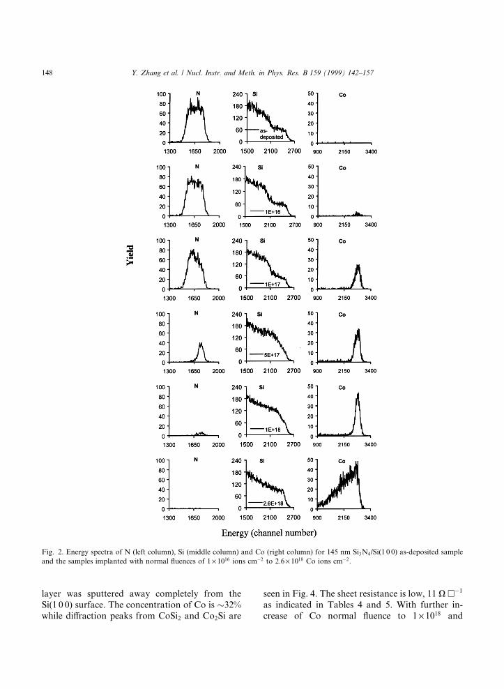
layer was sputtered away completely from theSi(1 0 0) surface. The concentration of Co is �32%while di�raction peaks from CoSi2 and Co2Si are
seen in Fig. 4. The sheet resistance is low, 11 X �ÿ1
as indicated in Tables 4 and 5. With further in-crease of Co normal ¯uence to 1 ´ 1018 and
Fig. 2. Energy spectra of N (left column), Si (middle column) and Co (right column) for 145 nm Si3N4/Si(1 0 0) as-deposited sample
and the samples implanted with normal ¯uences of 1 ´ 1016 ions cmÿ2 to 2.6 ´ 1018 Co ions cmÿ2.
148 Y. Zhang et al. / Nucl. Instr. and Meth. in Phys. Res. B 159 (1999) 142±157

2.6 ´ 1018 ions cmÿ2, roughening of the surfacetopography is observed [21], and Co penetratesdeeper. In the case of 1 ´ 1018 Co ions cmÿ2, onlyone crystalline phase with composition CoSi2 inthe implanted layer is identi®ed in the XRDspectrum, and the sheet resistance is greater (13.5
X �ÿ1). As one might expect, the thicker (145 nm)nitride ®lm protects the Si surface to a higher Conormal ¯uence (1 ´ 1018 ions cmÿ2) as compared tothe 72 nm ®lm. The implanted Co ions are local-ised within �80 nm from the surface except for thehighest Co normal ¯uence (2.6 ´ 1018 ions cmÿ2).
Fig. 3. Depth pro®les of C (A, a), N (B, b), O(C, c), Si (D, d) and Co (E, e) for 72 (left column) and 145 nm (right column) Si3N4/
Si(1 0 0) samples implanted by Co with di�erent Co normal ¯uences.
Y. Zhang et al. / Nucl. Instr. and Meth. in Phys. Res. B 159 (1999) 142±157 149

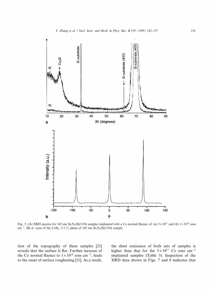
In the case of the 145 nm nitride sample implantedwith a normal ¯uence of 1 ´ 1018 Co ions cmÿ2, nopeaks attributable to CoSi2 are observed in theXRD data (Fig. 5a, line b). A / scan around the(1 1 1) re¯ection (Fig. 5B) con®rmed the presenceof CoSi2. This observation is in agreement with thelow sheet resistance (Table 4). In the case of5 ´ 1017 Co ions cmÿ2, the CoSi2 has also beenformed during the implantation. The high sheetresistance (150 X �ÿ1) of this sample might bedue to incomplete removal of the nitride layer(Fig. 3b).
The optimum condition to achieve a smooththin Co containing layer with a sharp interface(suitable for formation of a continuous CoSi2 ®lmby post-implantation annealing) is a normal ¯ue-nce of 5 ´ 1017 and 1018 Co ions cmÿ2 for 72 and145 nm thick nitride ®lms, respectively. As onemight anticipate, the Co ¯uence required to com-pletely remove the nitrogen increases with in-creasing ®lm thickness.
3.3. Co implantation into SiO2/Si samples
142 nm SiO2/Si(1 1 1) and 144 nm SiO2/(1 0 0)samples were implanted with Co normal ¯uences
from 1 ´ 1017 to 2.6 ´ 1018 ions cmÿ2. Judging fromthe O and Si depth distributions for un-implantedsamples (Fig. 6b, B, c and C), the composition ofthe thin ®lm closely corresponds to that of SiO2
within the expected uncertainty of 15% [20]. AfterCo implantation, the stoichiometry measured forthe near-surface region suggests a composition ofCoSi2 (Fig. 6 and Table 5) except for the lowest Conormal ¯uence, which is con®rmed by the XRDpeaks (shown in Figs. 7 and 8) and the electricalmeasurements (listed in Table 5).
Inspection of the plots in Fig. 6 permits thefollowing observations to be made. At an im-planted normal ¯uence of 1 ´ 1017 ions cmÿ2, thestoichiometry is disturbed. The atomic ratio of Oto Si decreases. This indicates that O is more easyto be ejected from the ®lm than Si [20]. This is inagreement with the studies of O and Si partialsputtering yield discussed in Part II [20]. At anormal ¯uence of 5 ´ 1017 Co ions cmÿ2, the oxidelayers are almost completely removed and theatomic fraction of Co at the surface approachesthat of CoSi2 for both sets of samples. In the XRDspectrum, CoSi2 peaks can be identi®ed. Thebroad weak peak �2h � 18�� visible in the XRDspectrum (Fig. 7a) is attributed to Co2Si. Inspec-
Fig. 4. XRD spectra for 72 nm Si3N4/Si(1 0 0) samples implanted with a Co normal ¯uence of: (a) 5 ´ 1017 and (b) 1 ´ 1018 ions cmÿ2.
150 Y. Zhang et al. / Nucl. Instr. and Meth. in Phys. Res. B 159 (1999) 142±157
tion of the topography of these samples [21]reveals that the surface is ¯at. Further increase ofthe Co normal ¯uence to 1 ´ 1018 ions cmÿ2, leadsto the onset of surface roughening [21]. As a result,
the sheet resistance of both sets of samples ishigher than that for the 5 ´ 1017 Co ions cmÿ2
implanted samples (Table 5). Inspection of theXRD data shown in Figs. 7 and 8 indicates that
Fig. 5. (A) XRD spectra for 145 nm Si3N4/Si(1 0 0) samples implanted with a Co normal ¯uence of: (a) 5 ´ 1017 and (b) 1 ´ 1018 ions
cmÿ2. (B) /ÿscan of the CoSi2 {1 1 1} plane of 145 nm Si3N4/Si(1 0 0) sample.
Y. Zhang et al. / Nucl. Instr. and Meth. in Phys. Res. B 159 (1999) 142±157 151

the CoSi2 phase is formed in both (1 1 1) and (1 0 0)samples. Other peaks, which are attributed toCo2Si, appear in the (1 0 0) sample (Fig. 8). At theextremely high Co normal ¯uence (2.6 ´ 1018 ionscmÿ2), the Co ions extend much deeper than therange estimated from SRIM 98 [30]. This is mostlikely due to the fact that the surfaces are com-pletely disrupted [21]. Evidence for this is that deepCo tails appear in both SiO2/Si(1 0 0) and SiO2/Si(1 1 1) samples (Fig. 6D and 6d). Moreover, itmay be seen that the content of C impurities in-creased which is most probably also a consequenceof the surface roughening (discussed below).
Fig. 6 and SEM results [21] indicate that 5 ´ 1017
ions cmÿ2 is an optimum Co normal ¯uence toremove the SiO2 coating ®lms and to obtain thinsilicide surface layers. Moreover, slightly betterstoichiometry of the CoSi2 layer, sharper interface,
and smother topography can be observed forSi(1 1 1) samples than for Si(1 0 0) samples.
3.4. Study of C and O contamination
C and O incorporation has been studied by Coimplantation into bare Si(1 1 1) and Si(1 0 0) sam-ples. Inspection of Fig. 1 indicates that the C andO signals, which are observed in all the baresamples, are only signi®cant at the surface forlower Co ¯uence samples. At higher Co normal¯uences, 5 ´ 1017 and 1 ´ 1018 ions cmÿ2, an in-crease of C and O concentrations below the sur-face is observed. The SEM results and Fig. 1indicate that for the low Co normal ¯uences wherethe surface remained smooth (Fig. 1a and b in Ref.[21]) the contaminants are located at the surface.At Co normal ¯uences of 5 ´ 1017 ions cmÿ2 or
Table 4
Calculated near-surface compositions from ERD data for nitride samples implanted with di�erent Co normal ¯uences, observed XRD
phases and measured sheet resistance from the four-point probe system
Si3N4 thickness
(nm)
Co normal ¯uence
(ions cmÿ2)
Silicide compositiona XRD phases Sheet resistance
(X �ÿ1)Co Si
72 5 ´ 1017 0.317 0.619 CoSi2, Co2Si 11.0
72 1 ´ 1018 0.315 0.641 CoSi2 13.5
145 5 ´ 1017 0.233 0.491 CoSi2 150
145 1 ´ 1018 0.283 0.614 CoSi2 35.6
a The relative uncertainty, which results from counting statistic, detection e�ciency and energy resolution, is less than �6%. The
absolute uncertainty due to the stopping power uncertainty is about �10%.
Table 5
Calculated near-surface compositions from ERD data for oxide samples implanted with di�erent Co normal ¯uences, observed XRD
phases and measured sheet resistance from the four-point probe system
SiO2
thickness (nm)
Substrate
orientation
Co normal
¯uence
(ions cmÿ2)
Silicide compositiona XRD phases Sheet resistance
(X �ÿ1)Co Si
142 1 1 1 5 ´ 1017 0.298 0.597 CoSi2, Co2Si 55.2
142 1 1 1 1 ´ 1018 0.271 0.685 CoSi2 64.8
144 1 0 0 5 ´ 1017 0.258 0.635 CoSi2 19.7
144 1 0 0 1 ´ 1018 0.233 0.701 CoSi2, Co2Si 69.8
a The relative uncertainty, which results from counting statistic, detection e�ciency and energy resolution, is less than �6%. The
absolute uncertainty due to the stopping power uncertainty is about �10%.
152 Y. Zhang et al. / Nucl. Instr. and Meth. in Phys. Res. B 159 (1999) 142±157

higher, topographic roughening has taken place(Figs. 1 and 2 in Ref. [21]), and the O and Ccontents below the surface were enhanced. Theseobservations imply for both Si(1 1 1) and (1 0 0)samples, that C and O were associated with surfacecontamination, and most probably originatedfrom exposure to atmosphere between implanta-
tion and analysis. With the consequential increasein surface area due to the higher Co ¯uencebombardment, proportionally more C and Ocould be absorbed. Moreover, because pores de-veloped on the sample surfaces, both implantedCo ions and C and O contaminants could pene-trate deeper into the bulk of the high ¯uence
Fig. 6. Depth pro®les of C (A, a), O (B, b), Si (C, c) and Co (D, d) for 142 nm SiO2/Si(1 1 1) (left column) and 144 nm SiO2/Si(1 0 0)
(right column) samples implanted by Co to di�erent normal ¯uences.
Y. Zhang et al. / Nucl. Instr. and Meth. in Phys. Res. B 159 (1999) 142±157 153

samples. (Here ``bulk'' means below the surfaceseen by ToF-E ERD.)
C and O incorporation has also been investi-gated in the oxide and nitride samples (Figs. 3 and
6). In all these coated samples, the contaminationconcentration is higher at, or near, the surfaceexcept for the higher Co normal ¯uences (1 ´ 1018
and 2.6 ´ 1018 ions cmÿ2). It is worth noting that
Fig. 7. XRD spectra for 142 nm SiO2/Si(1 1 1) samples implanted with a Co normal ¯uence of: (a) 5 ´ 1017 and (b) 1 ´ 1018 ions cmÿ2.
Fig. 8. XRD spectra for 144 nm SiO2/Si(1 0 0) samples implanted with a Co normal ¯uence of: (a) 5 ´ 1017 and (b) 1 ´ 1018 ions cmÿ2.
154 Y. Zhang et al. / Nucl. Instr. and Meth. in Phys. Res. B 159 (1999) 142±157

both the C and O signals are con®ned to a rangeshorter than the Co range, and do not show evi-dence of deeper penetration except for the higher¯uence samples (Figs. 1, 3 and 6). C and O fromthe source material would be accelerated to thesame energy as the Co beam, and penetrate deeperbecause of their smaller atomic number. Althoughthere is no magnetic separation used during theimplantation, the evidence implies that the co-im-plantation from the source can be ruled out as acause for the observed contamination by C and O[19].
Here we consider the nitride samples as exam-ples because in the case of the oxide samples the16O contamination cannot be distinguished from16O in the SiO2 coating layer. Fig. 9 presents thetotal amount of C and O contamination within the72 and 145 nm nitride/Si(1 0 0) samples as a func-tion of the implanted Co normal ¯uence. The dataindicate that the total amount of the contamina-tion at ®rst decreases with increasing Co ¯uence,and then increases dramatically as the Co ¯uenceincreases further. This observation implies that theC and O contamination does not originate fromthe implantation, otherwise the concentrationwould increase even for the low ¯uence samples.This agrees with the result from Fig. 1 that thecontamination is most probably formed on thesurface when the samples were exposed to air afterimplantation. The increase in C and O content at
high Co ¯uences is then a consequence of the in-crease in surface area associated with the devel-opment of a rough surface topography.Furthermore, one important point can be inferredfrom the oxygen content of the irradiated nitride®lms (Fig. 9) and its depth distribution (Fig. 3). Inthe low Co ¯uence region before a rough surfacetopography develops, oxygen is incorporated onlyon the surface and the total coverage does notexceed 2 ´ 1016 atoms cmÿ2. This is much less thanthe O content of the oxide ®lms. Thus we arecon®dent that the post-implantation exposure toatmosphere does not interfere with the results forO and N incorporation.
3.5. Removal of the surface layer of SiO2/Si andSi3N4/Si samples
An interesting question for technological ap-plications is whether a layer containing only Coand Si can be produced by bombarding a Si3N4/Sior SiO2/Si structure. Fig. 10 shows the retention ofO and N versus Co retention in the samples. Itmay be seen that for the �145 nm thick oxide andnitride ®lms there is a sharp decrease in the O andN content at a Co content of �8� 1016 ions cmÿ2.In the case of the 72 nm nitride ®lm sample it is notpossible to uniquely determine if the transition issharp due to the large Co normal ¯uence intervalin the data. The implication of the results in
Fig. 9. The content of C and O in the nitride samples implanted
by di�erent Co normal ¯uences.
Fig. 10. Total O and N contents vs. amount of Co incorporated
in the samples.
Y. Zhang et al. / Nucl. Instr. and Meth. in Phys. Res. B 159 (1999) 142±157 155

Fig. 10 is that no signi®cant amounts of O and Natoms were transported deep into the bulk by re-coil implantation, mixing and radiation-enhanceddi�usion. The slight increase of O content seenin the limit of high Co retention is associated withthe absorption on the roughened surface duringthe post-implantation exposure to atmosphere. Theresults of Figs. 3 and 10, and the ®ndings of thesputtering study [20] indicate that there exists anormal ¯uence range where the nitride/oxide ®lmis completely removed to leave a surface with ¯attopography [21] and a Co/Si atomic ratio thatcorresponds to CoSi2.
In order to function as a satisfactory litho-graphic mask material, a surface layer must com-pletely stop implanted ions after a particle normal¯uence (�5� 1017 ions cmÿ2) corresponding tothat required to achieve a silicide on unexposedsilicon [18]. It follows that a much thicker mask(�800 nm) than the thickness (145 nm) used here isneeded. This thickness requirement limits attain-able feature size because of the di�culty of etchingdeep high aspect ratio structures.
4. Conclusions
(i) A thin (�80 nm) silicide surface layer can beobtained by Co implantation using a MEVVA ionsource through a SiO2 or Si3N4 coating layer ontop of Si(1 1 1) or Si(1 0 0) substrates. The com-position of this layer mainly corresponds to CoSi2
with both smooth surface topography and sharpinterface to Si.
(ii) The optimum Co normal ¯uence to obtainthin silicide layers with a sharp interface andsmooth surface is governed by the oxide/nitridelayer thickness.
(iii) The MEVVA process is a promising tech-nique to form pure silicides. The contamination ofC and O is most probably associated with ab-sorption during the exposure to the atmospherebetween implantation and analysis.
Acknowledgements
We are grateful to the sta� at the Tandem Ac-celerator Laboratory in Uppsala and the Institute
of Low Energy Nuclear Physics, Beijing NormalUniversity for help and assistance. This investiga-tion has been carried out under the auspices of theNFR/NUTEK Nanometer Structure Consortium.
References
[1] J.W. Mayer, S.S. Lau, Electronic Materials Science for
Integrated Circuits in Si and GaAs, Macmillan, New York,
1990, p. 284.
[2] H. Reader, A.H. Van Homme, P.J.W. Weijs, R.A.M.
Wolters, D.J. Oostra, Rep. Prog. Phys. 56 (1933) 1397.
[3] D. Mangelinck, P. Gas, A. Grob, B. Pichaud, O. Thomas,
J. Appl. Phys. 79 (1996) 4078.
[4] J.S. Byun, D. Kim, S. Kim, H.J. Kim, J. Appl. Phys. 78
(1995) 1725.
[5] A.E. White, K.T. Short, R.C. Dynes, R. Hull, J.M.
Vandenberg, Nucl. Instr. and Meth. B 39 (1989) 253.
[6] D. Mangelinck, J. Cardenas, B.G. Svensson, Microelec-
tron. Eng. 37/38 (1997) 467.
[7] F.L. Via, A. Alberti, V. Raineri, S. Ravesi, E. Rimini,
Microelectron. Eng. 37/38 (1997) 475.
[8] B. Gebhardt, M. Falke, H. Giesler, S. Teichert, G.
Beddies, H.-j. Hinneberg, Microelectron. Eng. 37/38
(1997) 483.
[9] A. Terrasi, F.L. Via, F. D'Acapito, S. Mobilio, Micro-
electron. Eng. 37/38 (1997) 491.
[10] F. Klinkhammer, M. Dolle, L. Kappius, S. Mantl,
Microelectron. Eng. 37/38 (1997) 515.
[11] E.G. Colgan, J.P. Gambino, Q.Z. Hong, Mater. Sci. Eng.
R 16 (1996) 43.
[12] Y. Gao, Y.J. Yu, D.L. Tang, Y.M. Huang, M. Geng, X.R.
Gong, Rev. Sci. Instrum. 65 (1994) 1281.
[13] B.H. Sun, S. Hu, Q. Chen, Y. Shui, Rev. Sci. Instrum. 65
(1994) 1266.
[14] C.E. Chen, W. Zhao, Rev. Sci. Instrum. 67 (1996) 1399.
[15] H.X. Zhang, X.J. Zhang, F.S. Zhou, Q. Li, F.H. Liu, Z.E.
Han, W.L. Lin, Rev. Sci. Instrum. 65 (4) (1994) 1295.
[16] X.J. Zhang, F.S. Zhou, H.X. Zhang, S.J. Zhang, Q. Li,
Z.E. Han, Rev. Sci. Instrum. 63 (1992) 2431.
[17] F.S. Zhou, X.Y. Wu, F. Zhou, H.X. Zhang, X.J. Zhang,
Rev. Sci. Instrum. 65 (1994) 1263.
[18] Y. Zhang, H.J. Whitlow, T. Zhang, Microelectron. Eng.
37/38 (1997) 499.
[19] Y. Zhang, H.J. Whitlow, T. Zhang, Nucl. Instr. and Meth.
B 135 (1998) 392.
[20] Y. Zhang, T. Winzell, T. Zhang, I.A. Maximov, E-L.
Sarwe, M. Graczyk, L. Montelius, H.J. Whitlow, this
issue, Nucl. Instr. and Meth. B 159 (1999) 133.
[21] Y. Zhang, T. Winzell, T. Zhang, I.A. Maximov, E-L.
Sarwe, M. Graczyk, L. Montelius, H.J. Whitlow, this
issue, Nucl. Instr. and Meth. B 159 (1999) 158.
[22] X. Zhang, F. Zhou, H. Zhang, S. Zhang, Q. Li, Z. Han,
Rev. Sci. Instrum. 63 (1992) 2431.
[23] T. Zhang, C. Ji, J. Shen, J. Yang, J. Chen, Y. Gao, G. Sun,
Nucl. Instr. and Meth. B 59/60 (1991) 828.
156 Y. Zhang et al. / Nucl. Instr. and Meth. in Phys. Res. B 159 (1999) 142±157

[24] Y. Zhang, H.J. Whitlow, T. Winzell, I.F. Bubb,
T. Sajavaara, J. Jokinen, K. Arstila, J. Keinonen, Nucl.
Instr. and Meth. B 149 (1999) 477.
[25] F. Busch, W. Pfe�er, B. Kohlmeyer, D. Schull,
F. Puhlho�er, Nucl. Instr. and Meth. 171 (1980) 71.
[26] H.J. Whitlow, G. Possnert, C.S. Petersson, Nucl. Instr.
and Meth. B 27 (1987) 448.
[27] H.J. Whitlow, B. Jakonasson, L. Westerberg, Nucl. Instr.
and Meth. A 310 (1991) 636.
[28] M. Hult, H.J. Whitlow, M. �Ostling, M. Andersson,
Y. Andersson, I. Lindeberg, K. St�ahl, J. Appl. Phys. 75
(1994) 835.
[29] M. El Bouanani, M. Hult, L. Persson, E. Swietlicki, M.
Andersson, M. �Ostling, N. Lundberg, C. Zaring, D.D.
Cohen, N. Dytlewski, P.N. Johnston, S.R. Walker, I.F.
Bubb, H.J. Whitlow, Nucl. Instr. and Meth. B 94 (1994)
530.
[30] H.J. Whitlow, Turbo AnalysiS Support (TASS) for ERDA
data analysis using Physics Analysis Workstation, (CERN
Software Library, Switzerland, 1995), 1993.
[31] J.F. Ziegler, J.P. Biersack, U. Littmark, The Stopping and
Range of Ions in Solids, vol. 1, Pergamon Press, New
York, 1985. See also J.F. Ziegler, SRIM instruction
manual, 1998.
[32] T.B. Massalski (Ed.), Binary Alloy Phase Diagrams,
Metals Park, Ohio: American Society for Metals, 1986.
[33] T. Jorge, S. Yves, T. Patrick, Forward Recoil Spectrom-
etry, Plenum Press, New York, 1996.
Y. Zhang et al. / Nucl. Instr. and Meth. in Phys. Res. B 159 (1999) 142±157 157