high-efficiency, low-iq, pmics with dynamic voltage ... · max8660/max8660a/max8660b/max8661...
TRANSCRIPT
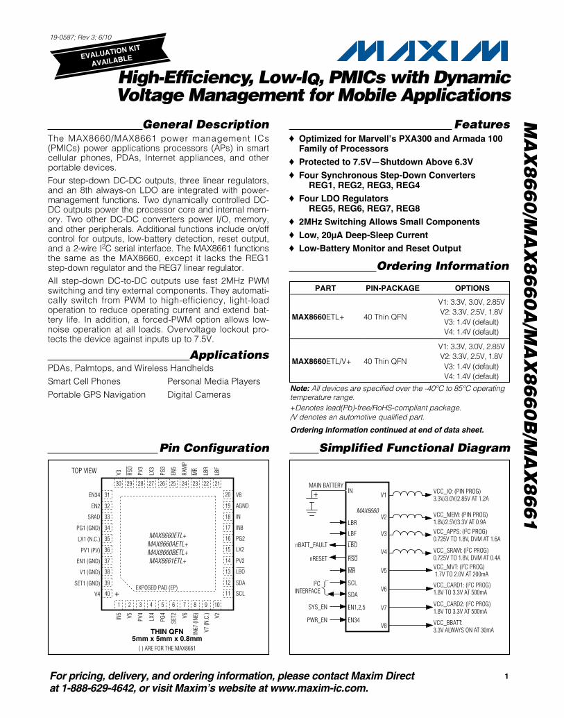
General DescriptionThe MAX8660/MAX8661 power management ICs(PMICs) power applications processors (APs) in smartcellular phones, PDAs, Internet appliances, and otherportable devices.Four step-down DC-DC outputs, three linear regulators,and an 8th always-on LDO are integrated with power-management functions. Two dynamically controlled DC-DC outputs power the processor core and internal mem-ory. Two other DC-DC converters power I/O, memory,and other peripherals. Additional functions include on/offcontrol for outputs, low-battery detection, reset output,and a 2-wire I2C serial interface. The MAX8661 functionsthe same as the MAX8660, except it lacks the REG1step-down regulator and the REG7 linear regulator.All step-down DC-to-DC outputs use fast 2MHz PWMswitching and tiny external components. They automati-cally switch from PWM to high-efficiency, light-loadoperation to reduce operating current and extend bat-tery life. In addition, a forced-PWM option allows low-noise operation at all loads. Overvoltage lockout pro-tects the device against inputs up to 7.5V.
ApplicationsPDAs, Palmtops, and Wireless Handhelds
Smart Cell Phones Personal Media Players
Portable GPS Navigation Digital Cameras
Features Optimized for Marvell’s PXA300 and Armada 100
Family of Processors
Protected to 7.5V—Shutdown Above 6.3V
Four Synchronous Step-Down ConvertersREG1, REG2, REG3, REG4
Four LDO RegulatorsREG5, REG6, REG7, REG8
2MHz Switching Allows Small Components
Low, 20µA Deep-Sleep Current
Low-Battery Monitor and Reset Output
MA
X8
66
0/M
AX
86
60
A/M
AX
86
60
B/M
AX
86
61
High-Efficiency, Low-IQ, PMICs with DynamicVoltage Management for Mobile Applications
Ordering Information
19-0587; Rev 3; 6/10
1For pricing, delivery, and ordering information, please contact Maxim Directat 1-888-629-4642, or visit Maxim’s website at www.maxim-ic.com.
EVALUATION KIT
AVAILABLE
PART PIN-PACKAGE OPTIONS
MAX8660ETL+ 40 Thin QFN
V 1: 3.3V , 3.0V , 2.85V V 2: 3.3V , 2.5V , 1.8V V 3: 1.4V ( d efaul t) V 4: 1.4V ( d efaul t)
MAX8660ETL/V+ 40 Thin QFN
V 1: 3.3V , 3.0V , 2.85V V 2: 3.3V , 2.5V , 1.8V V 3: 1.4V ( d efaul t) V 4: 1.4V ( d efaul t)
Note: All devices are specified over the -40°C to 85°C operatingtemperature range.+Denotes lead(Pb)-free/RoHS-compliant package./V denotes an automotive qualified part.
MAX8660ETL+MAX8660AETL+MAX8660BETL+MAX8661ETL+
THIN QFN5mm x 5mm x 0.8mm
( ) ARE FOR THE MAX8661
TOP VIEW
35
36
34
33
12
11
13
V5 LX4
PG4
SET2 V6
14
IN5
LX3
EN5
RAM
P
PV3
RSO
V3 MR
LBR
1 2
PG1 (GND)
4 5 6 7
27282930 26 24 23 22
LX1 (N.C.)
PV1 (PV)
IN
IN8
PG2
LX2
PV4
PG3
3
25
37EN1 (GND) PV2
38
39
40
V1 (GND)
SET1 (GND)
V4
LBO
SDA
SCL
SRAD
32
15
AGNDEN2
31
16
17
18
19
20 V8
IN67
(IN6
)
V7 (N
.C.) V2
LBF
8 9 10
21
EN34
EXPOSED PAD (EP)
Pin Configuration
V1
V2
V3
V4
V5
V6
V7
VCC_IO: (PIN PROG) 3.3V/3.0V/2.85V AT 1.2A
VCC_MEM: (PIN PROG) 1.8V/2.5V/3.3V AT 0.9AVCC_APPS: (I2C PROG) 0.725V TO 1.8V, DVM AT 1.6A
VCC_SRAM: (I2C PROG) 0.725V TO 1.8V, DVM AT 0.4AVCC_MVT: (I2C PROG) 1.7V TO 2.0V AT 200mA
VCC_CARD1: (I2C PROG)1.8V TO 3.3V AT 500mA
VCC_CARD2: (I2C PROG) 1.8V TO 3.3V AT 500mA
MR
RSO
LBR
LBO
EN1,2,5
EN34
nRESET
nBATT_FAULT
SYS_EN
PWR_EN
MAIN BATTERYIN
V8 VCC_BBATT: 3.3V ALWAYS ON AT 30mA
LBF
I2CINTERFACE
SCL
SDA
MAX8660
Simplified Functional Diagram
Ordering Information continued at end of data sheet.
MA
X8
66
0/M
AX
86
60
A/M
AX
86
60
B/M
AX
86
61
High-Efficiency, Low-IQ, PMICs with DynamicVoltage Management for Mobile Applications
2
Table of ContentsGeneral Description . . . . . . . . . . . . . . . . . . . . . . . . . . . . . . . . . . . . . . . . . . . . . . . . . . . . . . . . . . . . . . . . . . . . . . . . . . . 1
Applications . . . . . . . . . . . . . . . . . . . . . . . . . . . . . . . . . . . . . . . . . . . . . . . . . . . . . . . . . . . . . . . . . . . . . . . . . . . . . . . . . 1
Features . . . . . . . . . . . . . . . . . . . . . . . . . . . . . . . . . . . . . . . . . . . . . . . . . . . . . . . . . . . . . . . . . . . . . . . . . . . . . . . . . . . . 1
Ordering Information . . . . . . . . . . . . . . . . . . . . . . . . . . . . . . . . . . . . . . . . . . . . . . . . . . . . . . . . . . . . . . . . . . . . . . . . . . . 1
Simplified Functional Diagram . . . . . . . . . . . . . . . . . . . . . . . . . . . . . . . . . . . . . . . . . . . . . . . . . . . . . . . . . . . . . . . . . . . 1
Pin Configuration . . . . . . . . . . . . . . . . . . . . . . . . . . . . . . . . . . . . . . . . . . . . . . . . . . . . . . . . . . . . . . . . . . . . . . . . . . . . . . 1
Table of Contents . . . . . . . . . . . . . . . . . . . . . . . . . . . . . . . . . . . . . . . . . . . . . . . . . . . . . . . . . . . . . . . . . . . . . . . . . . . . . .2
Absolute Maximum Ratings . . . . . . . . . . . . . . . . . . . . . . . . . . . . . . . . . . . . . . . . . . . . . . . . . . . . . . . . . . . . . . . . . . . . . 4
Electrical Characteristics . . . . . . . . . . . . . . . . . . . . . . . . . . . . . . . . . . . . . . . . . . . . . . . . . . . . . . . . . . . . . . . . . . . . . . . 4
Typical Operating Characteristics . . . . . . . . . . . . . . . . . . . . . . . . . . . . . . . . . . . . . . . . . . . . . . . . . . . . . . . . . . . . . . . 11
Pin Description . . . . . . . . . . . . . . . . . . . . . . . . . . . . . . . . . . . . . . . . . . . . . . . . . . . . . . . . . . . . . . . . . . . . . . . . . . . . . . 19
Detailed Description . . . . . . . . . . . . . . . . . . . . . . . . . . . . . . . . . . . . . . . . . . . . . . . . . . . . . . . . . . . . . . . . . . . . . . . . . . 25
Maxim vs. Marvell PXA3xx Terminology . . . . . . . . . . . . . . . . . . . . . . . . . . . . . . . . . . . . . . . . . . . . . . . . . . . . . . . 25
Step-Down DC-DC Converters (REG1–REG4) . . . . . . . . . . . . . . . . . . . . . . . . . . . . . . . . . . . . . . . . . . . . . . . . . .26REG1 (VCC_IO) Step-Down DC-DC Converter (MAX8660 Only) . . . . . . . . . . . . . . . . . . . . . . . . . . . . . . . .26REG2 (VCC_IO, VCC_MEM) Step-Down DC-DC Converters . . . . . . . . . . . . . . . . . . . . . . . . . . . . . . . . . . .26REG3 (VCC_APPS) Step-Down DC-DC Converters . . . . . . . . . . . . . . . . . . . . . . . . . . . . . . . . . . . . . . . . . .27REG4 (VCC_SRAM) Step-Down DC-DC Converters . . . . . . . . . . . . . . . . . . . . . . . . . . . . . . . . . . . . . . . . . .27REG1–REG4 Step-Down DC-DC Converter Operating Modes . . . . . . . . . . . . . . . . . . . . . . . . . . . . . . . . . .27REG1–REG4 Synchronous Rectification . . . . . . . . . . . . . . . . . . . . . . . . . . . . . . . . . . . . . . . . . . . . . . . . . . .27REG1/REG2 100% Duty-Cycle Operation (Dropout) . . . . . . . . . . . . . . . . . . . . . . . . . . . . . . . . . . . . . . . . . .27
Linear Regulators (REG5–REG8) . . . . . . . . . . . . . . . . . . . . . . . . . . . . . . . . . . . . . . . . . . . . . . . . . . . . . . . . . . . . 28REG5 (VCC_MVT, VCC_BG, VCC_OSC13M, VCC_PLL) . . . . . . . . . . . . . . . . . . . . . . . . . . . . . . . . . . . . . . 28REG6/REG7 (VCC_CARD1, VCC_CARD2) . . . . . . . . . . . . . . . . . . . . . . . . . . . . . . . . . . . . . . . . . . . . . . . . . 28REG8 (VCC_BBATT) Always-On Regulator . . . . . . . . . . . . . . . . . . . . . . . . . . . . . . . . . . . . . . . . . . . . . . . . 28
Ramp-Rate Control (RAMP) . . . . . . . . . . . . . . . . . . . . . . . . . . . . . . . . . . . . . . . . . . . . . . . . . . . . . . . . . . . . . . . . 28
Power Sequencing . . . . . . . . . . . . . . . . . . . . . . . . . . . . . . . . . . . . . . . . . . . . . . . . . . . . . . . . . . . . . . . . . . . . . . . 29Enable Signals (EN_, PWR_EN, SYS_EN, I2C) . . . . . . . . . . . . . . . . . . . . . . . . . . . . . . . . . . . . . . . . . . . . . . 29REG3/REG4 Enable (EN34, EN3, EN4) . . . . . . . . . . . . . . . . . . . . . . . . . . . . . . . . . . . . . . . . . . . . . . . . . . . 30Power Modes . . . . . . . . . . . . . . . . . . . . . . . . . . . . . . . . . . . . . . . . . . . . . . . . . . . . . . . . . . . . . . . . . . . . . . . 30Power-Up and Power-Down Timing . . . . . . . . . . . . . . . . . . . . . . . . . . . . . . . . . . . . . . . . . . . . . . . . . . . . . . 30Marvell PXA3xx Power Configuration Register (PCFR) . . . . . . . . . . . . . . . . . . . . . . . . . . . . . . . . . . . . . . . . 30
Voltage Monitors, Reset, and Undervoltage-Lockout Functions . . . . . . . . . . . . . . . . . . . . . . . . . . . . . . . . . . . . . 32Undervoltage and Overvoltage Lockout . . . . . . . . . . . . . . . . . . . . . . . . . . . . . . . . . . . . . . . . . . . . . . . . . . . 32Reset Output (RSO) and MR Input . . . . . . . . . . . . . . . . . . . . . . . . . . . . . . . . . . . . . . . . . . . . . . . . . . . . . . . 32Low-Battery Detector (LBO, LBF, LBR) . . . . . . . . . . . . . . . . . . . . . . . . . . . . . . . . . . . . . . . . . . . . . . . . . . . 32
Internal Off-Discharge Resistors . . . . . . . . . . . . . . . . . . . . . . . . . . . . . . . . . . . . . . . . . . . . . . . . . . . . . . . . . . . . . 33Thermal-Overload Protection . . . . . . . . . . . . . . . . . . . . . . . . . . . . . . . . . . . . . . . . . . . . . . . . . . . . . . . . . . . . . . . 33I2C Interface . . . . . . . . . . . . . . . . . . . . . . . . . . . . . . . . . . . . . . . . . . . . . . . . . . . . . . . . . . . . . . . . . . . . . . . . . . . . 33
Data Transfer . . . . . . . . . . . . . . . . . . . . . . . . . . . . . . . . . . . . . . . . . . . . . . . . . . . . . . . . . . . . . . . . . . . . . . . 33START and STOP Conditions . . . . . . . . . . . . . . . . . . . . . . . . . . . . . . . . . . . . . . . . . . . . . . . . . . . . . . . . . . . 35Acknowledge Bit . . . . . . . . . . . . . . . . . . . . . . . . . . . . . . . . . . . . . . . . . . . . . . . . . . . . . . . . . . . . . . . . . . . . . 35Slave Address . . . . . . . . . . . . . . . . . . . . . . . . . . . . . . . . . . . . . . . . . . . . . . . . . . . . . . . . . . . . . . . . . . . . . . . 35I2C Write Operation . . . . . . . . . . . . . . . . . . . . . . . . . . . . . . . . . . . . . . . . . . . . . . . . . . . . . . . . . . . . . . . . . . . 36

MA
X8
66
0/M
AX
86
60
A/M
AX
86
60
B/M
AX
86
61
High-Efficiency, Low-IQ, PMICs with DynamicVoltage Management for Mobile Applications
3
Table of Contents (continued)Design Procedure . . . . . . . . . . . . . . . . . . . . . . . . . . . . . . . . . . . . . . . . . . . . . . . . . . . . . . . . . . . . . . . . . . . . . . . . . . . . 38
Setting the Output Voltages . . . . . . . . . . . . . . . . . . . . . . . . . . . . . . . . . . . . . . . . . . . . . . . . . . . . . . . . . . . . . . . . 38Inductor Selection . . . . . . . . . . . . . . . . . . . . . . . . . . . . . . . . . . . . . . . . . . . . . . . . . . . . . . . . . . . . . . . . . . . . . . . . 38Input Capacitor Selection . . . . . . . . . . . . . . . . . . . . . . . . . . . . . . . . . . . . . . . . . . . . . . . . . . . . . . . . . . . . . . . . . . 39Output Capacitor Selection . . . . . . . . . . . . . . . . . . . . . . . . . . . . . . . . . . . . . . . . . . . . . . . . . . . . . . . . . . . . . . . . . 39Step-Down Converter Output Current . . . . . . . . . . . . . . . . . . . . . . . . . . . . . . . . . . . . . . . . . . . . . . . . . . . . . . . . . 39
Applications Information . . . . . . . . . . . . . . . . . . . . . . . . . . . . . . . . . . . . . . . . . . . . . . . . . . . . . . . . . . . . . . . . . . . . . . . 40Power Dissipation . . . . . . . . . . . . . . . . . . . . . . . . . . . . . . . . . . . . . . . . . . . . . . . . . . . . . . . . . . . . . . . . . . . . . . . . 40PCB Layout and Routing . . . . . . . . . . . . . . . . . . . . . . . . . . . . . . . . . . . . . . . . . . . . . . . . . . . . . . . . . . . . . . . . . . . 40
Package Marking . . . . . . . . . . . . . . . . . . . . . . . . . . . . . . . . . . . . . . . . . . . . . . . . . . . . . . . . . . . . . . . . . . . . . . . . . . . . 41
Chip Information . . . . . . . . . . . . . . . . . . . . . . . . . . . . . . . . . . . . . . . . . . . . . . . . . . . . . . . . . . . . . . . . . . . . . . . . . . . . . 41
Package Information . . . . . . . . . . . . . . . . . . . . . . . . . . . . . . . . . . . . . . . . . . . . . . . . . . . . . . . . . . . . . . . . . . . . . . . . . . 42
Revision History . . . . . . . . . . . . . . . . . . . . . . . . . . . . . . . . . . . . . . . . . . . . . . . . . . . . . . . . . . . . . . . . . . . . . . . . . . . . . . 44
TablesTable 1. Maxim and Marvell PXA3xx Power Domain Terminology . . . . . . . . . . . . . . . . . . . . . . . . . . . . . . . . . . . 25Table 2. Maxim and Marvell PXA3xx Digital Signal Terminology . . . . . . . . . . . . . . . . . . . . . . . . . . . . . . . . . . . . 26Table 3. SET1 Logic . . . . . . . . . . . . . . . . . . . . . . . . . . . . . . . . . . . . . . . . . . . . . . . . . . . . . . . . . . . . . . . . . . . . . . 26Table 4. SET2 Logic . . . . . . . . . . . . . . . . . . . . . . . . . . . . . . . . . . . . . . . . . . . . . . . . . . . . . . . . . . . . . . . . . . . . . . 26Table 5. Enable Signals . . . . . . . . . . . . . . . . . . . . . . . . . . . . . . . . . . . . . . . . . . . . . . . . . . . . . . . . . . . . . . . . . . . 29Table 6. Truth Table for V3/V4 Enable Logic . . . . . . . . . . . . . . . . . . . . . . . . . . . . . . . . . . . . . . . . . . . . . . . . . . . 30Table 7. Power Modes and Corresponding Quiescent Operating Currents . . . . . . . . . . . . . . . . . . . . . . . . . . . . 31Table 8. Internal Off-Discharge Resistor . . . . . . . . . . . . . . . . . . . . . . . . . . . . . . . . . . . . . . . . . . . . . . . . . . . . . . . 33Table 9. I2C Registers . . . . . . . . . . . . . . . . . . . . . . . . . . . . . . . . . . . . . . . . . . . . . . . . . . . . . . . . . . . . . . . . . . . . . 34Table 10. DVM Voltage Change Register (VCC1, 0x20) . . . . . . . . . . . . . . . . . . . . . . . . . . . . . . . . . . . . . . . . . . . 36Table 11. Serial Codes for V3 (VCC_APPS) and V4 (VCC_SRAM) Output Voltages. . . . . . . . . . . . . . . . . . . . . . 37Table 12. Serial Codes for V5 Output Voltage . . . . . . . . . . . . . . . . . . . . . . . . . . . . . . . . . . . . . . . . . . . . . . . . . . 37Table 13. Serial Codes for V6 and V7 Output Voltages . . . . . . . . . . . . . . . . . . . . . . . . . . . . . . . . . . . . . . . . . . . 37
FiguresFigure 1. Example MAX8660 Connection to Marvell PXA3xx Processor . . . . . . . . . . . . . . . . . . . . . . . . . . . . . . 22Figure 2. Functional Diagram . . . . . . . . . . . . . . . . . . . . . . . . . . . . . . . . . . . . . . . . . . . . . . . . . . . . . . . . . . . . . . . 23Figure 3. Typical Applications Circuit . . . . . . . . . . . . . . . . . . . . . . . . . . . . . . . . . . . . . . . . . . . . . . . . . . . . . . . . . 24Figure 4. Soft-Start and Voltage-Change Ramp Rates . . . . . . . . . . . . . . . . . . . . . . . . . . . . . . . . . . . . . . . . . . . . 28Figure 5. V3/V4 Enable Logic . . . . . . . . . . . . . . . . . . . . . . . . . . . . . . . . . . . . . . . . . . . . . . . . . . . . . . . . . . . . . . . 30Figure 6. Power-Up Timing . . . . . . . . . . . . . . . . . . . . . . . . . . . . . . . . . . . . . . . . . . . . . . . . . . . . . . . . . . . . . . . . . 31Figure 7. Low-Battery Detector Functional Diagram . . . . . . . . . . . . . . . . . . . . . . . . . . . . . . . . . . . . . . . . . . . . . . 32Figure 8. START and STOP Conditions . . . . . . . . . . . . . . . . . . . . . . . . . . . . . . . . . . . . . . . . . . . . . . . . . . . . . . . . 35Figure 9. Acknowledge Bits . . . . . . . . . . . . . . . . . . . . . . . . . . . . . . . . . . . . . . . . . . . . . . . . . . . . . . . . . . . . . . . . 35Figure 10. Slave Address Byte . . . . . . . . . . . . . . . . . . . . . . . . . . . . . . . . . . . . . . . . . . . . . . . . . . . . . . . . . . . . . . .35Figure 11. Writing to the MAX8660/MAX8661 . . . . . . . . . . . . . . . . . . . . . . . . . . . . . . . . . . . . . . . . . . . . . . . . . . .38Figure 12. Step-Down Converter Maximum Output Current Example . . . . . . . . . . . . . . . . . . . . . . . . . . . . . . . . .39
MA
X8
66
0/M
AX
86
60
A/M
AX
86
60
B/M
AX
86
61
High-Efficiency, Low-IQ, PMICs with DynamicVoltage Management for Mobile Applications
4
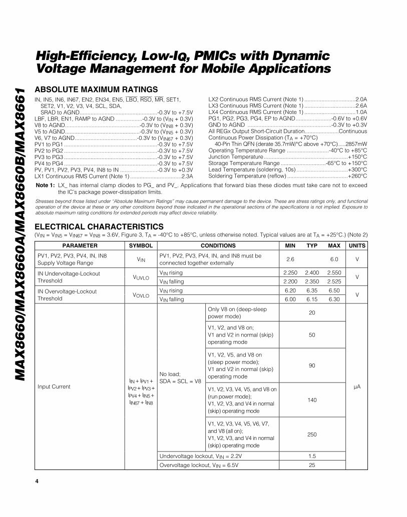
ABSOLUTE MAXIMUM RATINGS
ELECTRICAL CHARACTERISTICS(VIN = VIN5 = VIN67 = VIN8 = 3.6V, Figure 3, TA = -40°C to +85°C, unless otherwise noted. Typical values are at TA = +25°C.) (Note 2)
Stresses beyond those listed under “Absolute Maximum Ratings” may cause permanent damage to the device. These are stress ratings only, and functionaloperation of the device at these or any other conditions beyond those indicated in the operational sections of the specifications is not implied. Exposure toabsolute maximum rating conditions for extended periods may affect device reliability.
Note 1: LX_ has internal clamp diodes to PG_ and PV_. Applications that forward bias these diodes must take care not to exceedthe IC’s package power-dissipation limits.
IN, IN5, IN6, IN67, EN2, EN34, EN5, LBO, RSO, MR, SET1, SET2, V1, V2, V3, V4, SCL, SDA,SRAD to AGND..................................................-0.3V to +7.5V
LBF, LBR, EN1, RAMP to AGND .................-0.3V to (VIN + 0.3V)V8 to AGND................................................-0.3V to (VIN8 + 0.3V)V5 to AGND................................................-0.3V to (VIN5 + 0.3V)V6, V7 to AGND........................................-0.3V to (VIN67 + 0.3V)PV1 to PG1 ............................................................-0.3V to +7.5VPV2 to PG2 ............................................................-0.3V to +7.5VPV3 to PG3 ............................................................-0.3V to +7.5VPV4 to PG4 ............................................................-0.3V to +7.5VPV, PV1, PV2, PV3, PV4, IN8 to IN ........................-0.3V to +0.3VLX1 Continuous RMS Current (Note 1) .................................2.3A
LX2 Continuous RMS Current (Note 1) .................................2.0ALX3 Continuous RMS Current (Note 1) .................................2.6ALX4 Continuous RMS Current (Note 1) .................................1.0APG1, PG2, PG3, PG4, EP to AGND.......................-0.6V to +0.6VGND to AGND ......................................................-0.3V to +0.3VAll REGx Output Short-Circuit Duration......................ContinuousContinuous Power Dissipation (TA = +70°C)
40-Pin Thin QFN (derate 35.7mW/°C above +70°C).....2857mWOperating Temperature Range ...........................-40°C to +85°CJunction Temperature ......................................................+150°CStorage Temperature Range .............................-65°C to +150°CLead Temperature (soldering, 10s) .................................+300°CSoldering Temperature (reflow) .......................................+260°C
PARAMETER SYMBOL CONDITIONS MIN TYP MAX UNITS
PV1, PV2, PV3, PV4, IN, IN8Supply Voltage Range
VINPV1, PV2, PV3, PV4, IN, and IN8 must beconnected together externally
2.6 6.0 V
VIN rising 2.250 2.400 2.550IN Undervoltage-LockoutThreshold
VUVLOVIN falling 2.200 2.350 2.525
V
VIN rising 6.20 6.35 6.50IN Overvoltage-LockoutThreshold
VOVLOVIN falling 6.00 6.15 6.30
V
Only V8 on (deep-sleeppower mode)
20
V1, V2, and V8 on;V1 and V2 in normal (skip)operating mode
50
V1, V2, V5, and V8 on(sleep power mode);V1 and V2 in normal (skip)operating mode
90
V 1, V 2, V 3, V 4, V 5, and V 8 on( r un p ow er m od e) ;V 1, V 2, V 3, and V 4 i n nor m al ( ski p ) op er ati ng m od e
140
No load;SDA = SCL = V8
V 1, V 2, V 3, V 4, V 5, V 6, V 7,and V 8 ( al l on) ;V 1, V 2, V 3, and V 4 i n nor m al ( ski p ) op er ati ng m od e
250
Undervoltage lockout, VIN = 2.2V 1.5
Input CurrentIIN + IPV 1 +IPV 2 + IPV 3 +IPV 4 + IIN 5 +IIN 67 + IIN 8
Overvoltage lockout, VIN = 6.5V 25
µA

MA
X8
66
0/M
AX
86
60
A/M
AX
86
60
B/M
AX
86
61
High-Efficiency, Low-IQ, PMICs with DynamicVoltage Management for Mobile Applications
5
ELECTRICAL CHARACTERISTICS (continued)(VIN = VIN5 = VIN67 = VIN8 = 3.6V, Figure 3, TA = -40°C to +85°C, unless otherwise noted. Typical values are at TA = +25°C.) (Note 2)
PARAMETER SYMBOL CONDITIONS MIN TYP MAX UNITS
PWM Switching Frequency fSW 1.9 2.0 2.1 MHz
REG1—SYNCHRONOUS STEP-DOWN DC-DC CONVERTER (MAX8660, MAX8660A, MAX8660B only)
SET1 = IN, VPV1 = 4.2V, load = 600mA 3.250 3.300 3.350
SET1 not connected, VPV1 = 3.6V,load = 600mA
2.955 3.000 3.045V1 VoltageAccuracy (MAX8860/MAX8860B)
V1
SET1 = AGND, VPV1 = 3.6V, load = 600mA 2.807 2.850 2.893
V
SET1 = IN, VPV1 = 4.2V, load = 600mA 2.463 2.500 2.538
SET1 not connected, VPV1 = 3.6V,load = 600mA
1.970 2.000 2.030V 1 V ol tag e Accur acy ( M AX 8660A) V1
SET1 = AGND, VPV1 = 3.6V, load = 600mA 1.773 1.800 1.827
V
V1 Load Regulation Load = 0 to 1200mA -1.5 %/A
V1 Line Regulation 0.15 %/V
SET1 Input Leakage Current 0.01 µA
Load = 800mA (Notes 3, 4) 150V1 Dropout Voltage
Load = 1200mA (Notes 3, 4) 200mV
p-Channel On-Resistance RP1 0.12 Ωn-Channel On-Resistance RN1 0.15 Ω
p-Channel Current-LimitThreshold
ILIM1 1.5 1.8 2.2 A
n-Channel Zero-CrossingThreshold
25 mA
n-Channel Negative Current Limit Forced-PWM mode only -975 mA
REG1 Maximum Output Current IOUT1 2.6V ≤ VPV1 ≤ 6V (Note 5) 1.2 A
V1 Bias Current 5 µA
TA = +25°C -2 ±0.03 +2LX1 Leakage Current
VPV1 = 6V, LX1 =PG1 or PV1,VEN1 = 0V TA = +85°C ±0.2
µA
Soft-Start Ramp Rate(MAX8660/MAX8860B)
To V1 = 3.3V (total ramp time is 450µs forall V1 output voltages)
5 7 9 mV/µs
Soft-Start Ramp Rate(MAX8660A)
To V1 = 2.5V (total ramp time is 450µs forall V1 output voltages)
3 5 7 mV/µs
V5 to V1 Enable Time tVMHVSH1 Figure 6 350 µs
Internal Off-Discharge Resistance 650 Ω
Minimum Duty CycleForced-PWM mode only, min duty cycle inskip mode is 0%
16.7 %
Maximum Duty Cycle 100 %
MA
X8
66
0/M
AX
86
60
A/M
AX
86
60
B/M
AX
86
61
High-Efficiency, Low-IQ, PMICs with DynamicVoltage Management for Mobile Applications
6
ELECTRICAL CHARACTERISTICS (continued)(VIN = VIN5 = VIN67 = VIN8 = 3.6V, Figure 3, TA = -40°C to +85°C, unless otherwise noted. Typical values are at TA = +25°C.) (Note 2)
PARAMETER SYMBOL CONDITIONS MIN TYP MAX UNITS
REG2—SYNCHRONOUS STEP-DOWN DC-DC CONVERTERSET2 = IN, VPV2 = 4.2V, load = 600mA 3.250 3.300 3.350
SET2 not connected, VPV2 = 3.6V,load = 600mA
2.463 2.500 2.538V2 VoltageAccuracy (MAX8660/MAX8860B)
V2
SET2 = AGND, VPV2 = 3.6V, load = 600mA 1.773 1.800 1.827
V
SET2 = IN, VPV2 = 4.2V, load = 600mA 2.463 2.500 2.538
SET2 not connected, VPV2 = 3.6V,load = 600mA
1.970 2.000 2.030V2 Voltage Accuracy (MAX8660A) V2
SET2 = AGND, VPV2 = 3.6V, load = 600mA 1.773 1.800 1.827
V
V2 Load Regulation Load = 0 to 900mA -1.7 %/A
V2 Line Regulation 0.15 %/V
SET2 Input Leakage Current 0.01 µA
V2 Dropout Voltage Load = 900mA (Notes 3, 4) 225 mV
p-Channel On-Resistance RP2 0.18 Ωn-Channel On-Resistance RN2 0.15 Ωp-Channel Current-Limit Threshold ILIM2 1.10 1.30 1.50 A
n- C hannel Z er o C r ossi ng Thr eshol d 25 mA
n-Channel Negative Current Limit Forced-PWM mode only -800 mA
REG2 Maximum Output Current IOUT2 2.6V ≤ VPV2 ≤ 6V (Note 5) 0.9 A
V2 Bias Current 5 µA
TA = +25°C -2 ±0.03 +2LX2 Leakage Current
VPV2 = 6V,LX2 = PG2 or PV2,VEN2 = 0V TA = +85°C 0.2
µA
Soft-Start Ramp RateTo V2 = 1.8V (total ramp time is 450µs forall V2 output voltages)
2 4 6 mV/µs
V5 to V2 Enable Time tVMHVSH2 Figure 6 350 µs
Internal Off-Discharge Resistance 650 Ω
Minimum Duty CycleForced-PWM mode only; min duty cycle inskip mode is 0%
16.7 %
Maximum Duty Cycle 100 %
REG3—SYNCHRONOUS STEP-DOWN DC-DC CONVERTER
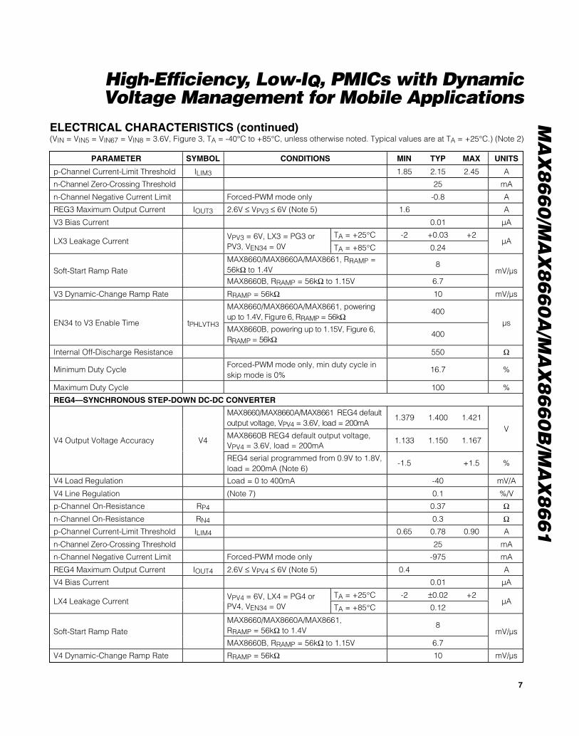
MAX8860/MAX8660A/MAX8661 REG3default output voltage, VPV3 = 3.6V,load = 600mA
1.379 1.400 1.421
MAX8860B REG3 default output voltage,VPV3 = 3.6V, load = 600mA
1.133 1.150 1.167
VV3 Output Voltage Accuracy V3
REG3 serial programmed from 0.9V to 1.8V,load = 600mA (Note 6)
-1.5 +1.5 %
V3 Load Regulation Load = 0 to 1600mA -17 mV/A
V3 Line Regulation (Note 7) 0.05 %/V
p-Channel On-Resistance RP3 0.12 Ωn-Channel On-Resistance RN3 0.08 Ω
MA
X8
66
0/M
AX
86
60
A/M
AX
86
60
B/M
AX
86
61
High-Efficiency, Low-IQ, PMICs with DynamicVoltage Management for Mobile Applications
7
ELECTRICAL CHARACTERISTICS (continued)(VIN = VIN5 = VIN67 = VIN8 = 3.6V, Figure 3, TA = -40°C to +85°C, unless otherwise noted. Typical values are at TA = +25°C.) (Note 2)
PARAMETER SYMBOL CONDITIONS MIN TYP MAX UNITS
p-Channel Current-Limit Threshold ILIM3 1.85 2.15 2.45 A
n- C hannel Z er o- C r ossi ng Thr eshol d 25 mA
n-Channel Negative Current Limit Forced-PWM mode only -0.8 A
REG3 Maximum Output Current IOUT3 2.6V ≤ VPV3 ≤ 6V (Note 5) 1.6 A
V3 Bias Current 0.01 µA
TA = +25°C -2 +0.03 +2LX3 Leakage Current
VPV3 = 6V, LX3 = PG3 orPV3, VEN34 = 0V TA = +85°C 0.24
µA
MAX8660/MAX8660A/MAX8661, RRAMP =56kΩ to 1.4V
8Soft-Start Ramp Rate
MAX8660B, RRAMP = 56kΩ to 1.15V 6.7mV/µs
V3 Dynamic-Change Ramp Rate RRAMP = 56kΩ 10 mV/µs
MAX8660/MAX8660A/MAX8661, pow er i ng up to 1.4V , Fi g ur e 6, RRAM P = 56kΩ
400EN34 to V3 Enable Time tPHLVTH3
MAX8660B, pow er i ng up to 1.15V , Fi g ur e 6,RRAM P = 56kΩ
400µs
Internal Off-Discharge Resistance 550 Ω
Minimum Duty CycleForced-PWM mode only, min duty cycle inskip mode is 0%
16.7 %
Maximum Duty Cycle 100 %
REG4—SYNCHRONOUS STEP-DOWN DC-DC CONVERTER
M AX 8660/M AX 8660A/M AX 8661 RE G4 d efaul toutp ut vol tag e, V P V 4 = 3.6V , l oad = 200m A
1.379 1.400 1.421
MAX8660B REG4 default output voltage,VPV4 = 3.6V, load = 200mA
1.133 1.150 1.167V
V4 Output Voltage Accuracy V4
REG4 serial programmed from 0.9V to 1.8V,load = 200mA (Note 6)
-1.5 +1.5 %
V4 Load Regulation Load = 0 to 400mA -40 mV/A
V4 Line Regulation (Note 7) 0.1 %/V
p-Channel On-Resistance RP4 0.37 Ωn-Channel On-Resistance RN4 0.3 Ωp-Channel Current-Limit Threshold ILIM4 0.65 0.78 0.90 A
n- C hannel Z er o- C r ossi ng Thr eshol d 25 mA
n-Channel Negative Current Limit Forced-PWM mode only -975 mA
REG4 Maximum Output Current IOUT4 2.6V ≤ VPV4 ≤ 6V (Note 5) 0.4 A
V4 Bias Current 0.01 µA
TA = +25°C -2 ±0.02 +2LX4 Leakage Current
VPV4 = 6V, LX4 = PG4 orPV4, VEN34 = 0V TA = +85°C 0.12
µA
MAX8660/MAX8660A/MAX8661,RRAMP = 56kΩ to 1.4V
8Soft-Start Ramp Rate
MAX8660B, RRAMP = 56kΩ to 1.15V 6.7mV/µs
V4 Dynamic-Change Ramp Rate RRAMP = 56kΩ 10 mV/µs
MA
X8
66
0/M
AX
86
60
A/M
AX
86
60
B/M
AX
86
61
High-Efficiency, Low-IQ, PMICs with DynamicVoltage Management for Mobile Applications
8
ELECTRICAL CHARACTERISTICS (continued)(VIN = VIN5 = VIN67 = VIN8 = 3.6V, Figure 3, TA = -40°C to +85°C, unless otherwise noted. Typical values are at TA = +25°C.) (Note 2)
PARAMETER SYMBOL CONDITIONS MIN TYP MAX UNITS
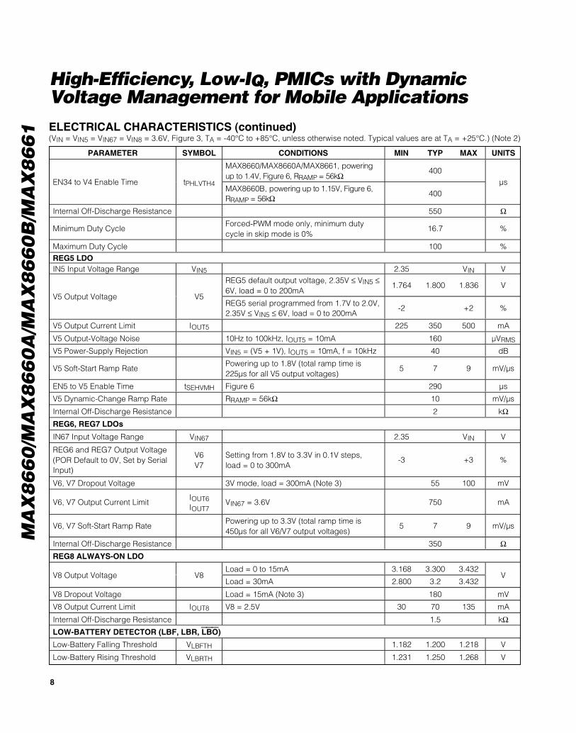
MAX8660/MAX8660A/MAX8661, pow er i ng up to 1.4V , Fi g ur e 6, RRAM P = 56kΩ
400EN34 to V4 Enable Time tPHLVTH4
MAX8660B, pow er i ng up to 1.15V , Fi g ur e 6,RRAM P = 56kΩ
400µs
Internal Off-Discharge Resistance 550 Ω
Minimum Duty CycleForced-PWM mode only, minimum dutycycle in skip mode is 0%
16.7 %
Maximum Duty Cycle 100 %REG5 LDOIN5 Input Voltage Range VIN5 2.35 VIN V
REG5 default output voltage, 2.35V ≤ VIN5 ≤6V, load = 0 to 200mA
1.764 1.800 1.836 VV5 Output Voltage V5
REG5 serial programmed from 1.7V to 2.0V,2.35V ≤ VIN5 ≤ 6V, load = 0 to 200mA
-2 +2 %
V5 Output Current Limit IOUT5 225 350 500 mA
V5 Output-Voltage Noise 10Hz to 100kHz, IOUT5 = 10mA 160 µVRMS
V5 Power-Supply Rejection VIN5 = (V5 + 1V), IOUT5 = 10mA, f = 10kHz 40 dB
V5 Soft-Start Ramp RatePowering up to 1.8V (total ramp time is225µs for all V5 output voltages)
5 7 9 mV/µs
EN5 to V5 Enable Time tSEHVMH Figure 6 290 µs
V5 Dynamic-Change Ramp Rate RRAMP = 56kΩ 10 mV/µs
Internal Off-Discharge Resistance 2 kΩREG6, REG7 LDOs
IN67 Input Voltage Range VIN67 2.35 VIN V
REG6 and REG7 Output Voltage(POR Default to 0V, Set by SerialInput)
V6V7
Setting from 1.8V to 3.3V in 0.1V steps,load = 0 to 300mA
-3 +3 %
V6, V7 Dropout Voltage 3V mode, load = 300mA (Note 3) 55 100 mV
V6, V7 Output Current LimitIOUT6IOUT7
VIN67 = 3.6V 750 mA
V6, V7 Soft-Start Ramp RatePowering up to 3.3V (total ramp time is450µs for all V6/V7 output voltages)
5 7 9 mV/µs
Internal Off-Discharge Resistance 350 ΩREG8 ALWAYS-ON LDO
Load = 0 to 15mA 3.168 3.300 3.432V8 Output Voltage V8
Load = 30mA 2.800 3.2 3.432V
V8 Dropout Voltage Load = 15mA (Note 3) 180 mV
V8 Output Current Limit IOUT8 V8 = 2.5V 30 70 135 mA
Internal Off-Discharge Resistance 1.5 kΩLOW-BATTERY DETECTOR (LBF, LBR, LBO)
Low-Battery Falling Threshold VLBFTH 1.182 1.200 1.218 V
Low-Battery Rising Threshold VLBRTH 1.231 1.250 1.268 V
MA
X8
66
0/M
AX
86
60
A/M
AX
86
60
B/M
AX
86
61
High-Efficiency, Low-IQ, PMICs with DynamicVoltage Management for Mobile Applications
9
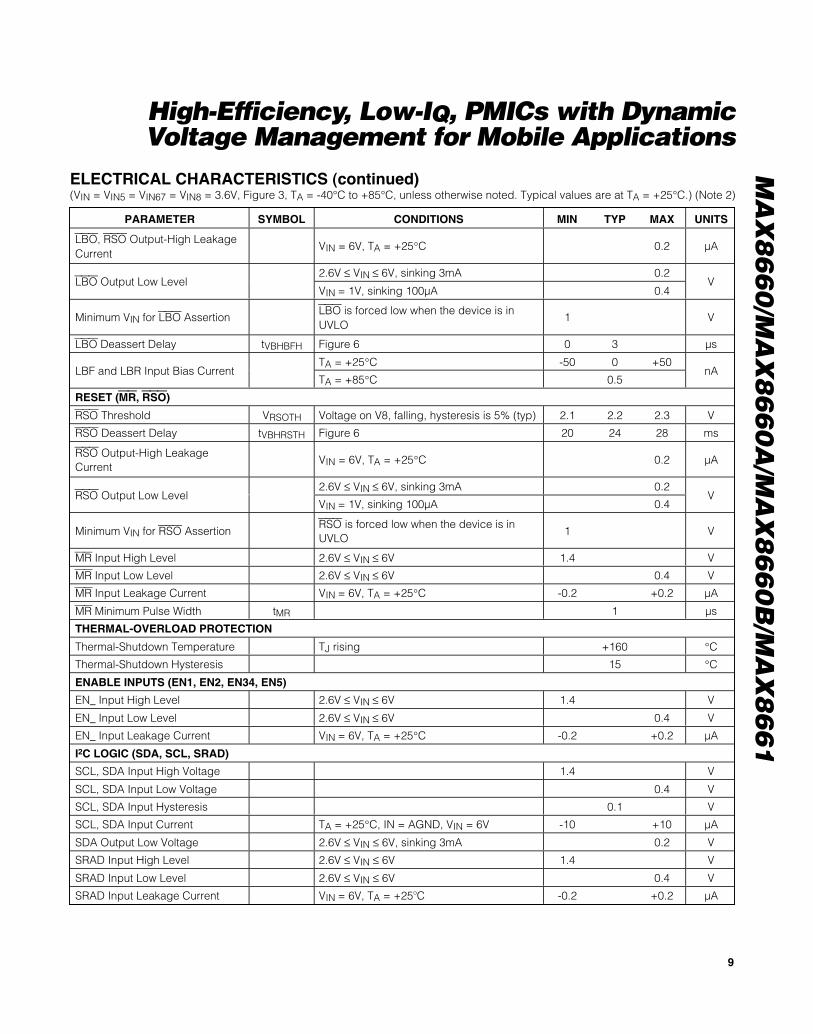
ELECTRICAL CHARACTERISTICS (continued)(VIN = VIN5 = VIN67 = VIN8 = 3.6V, Figure 3, TA = -40°C to +85°C, unless otherwise noted. Typical values are at TA = +25°C.) (Note 2)
PARAMETER SYMBOL CONDITIONS MIN TYP MAX UNITS
LBO, RSO Output-High LeakageCurrent
VIN = 6V, TA = +25°C 0.2 µA
2.6V ≤ VIN ≤ 6V, sinking 3mA 0.2LBO Output Low Level
VIN = 1V, sinking 100µA 0.4V
Minimum VIN for LBO AssertionLBO is forced low when the device is inUVLO
1 V
LBO Deassert Delay tVBHBFH Figure 6 0 3 µs
TA = +25°C -50 0 +50LBF and LBR Input Bias Current
TA = +85°C 0.5nA
RESET (MR, RSO)
RSO Threshold VRSOTH Voltage on V8, falling, hysteresis is 5% (typ) 2.1 2.2 2.3 V
RSO Deassert Delay tVBHRSTH Figure 6 20 24 28 ms
RSO Output-High LeakageCurrent
VIN = 6V, TA = +25°C 0.2 µA
2.6V ≤ VIN ≤ 6V, sinking 3mA 0.2RSO Output Low Level
VIN = 1V, sinking 100µA 0.4V
Minimum VIN for RSO AssertionRSO is forced low when the device is inUVLO
1 V
MR Input High Level 2.6V ≤ VIN ≤ 6V 1.4 V
MR Input Low Level 2.6V ≤ VIN ≤ 6V 0.4 V
MR Input Leakage Current VIN = 6V, TA = +25°C -0.2 +0.2 µA
MR Minimum Pulse Width tMR 1 µs
THERMAL-OVERLOAD PROTECTION
Thermal-Shutdown Temperature TJ rising +160 °C
Thermal-Shutdown Hysteresis 15 °C
ENABLE INPUTS (EN1, EN2, EN34, EN5)
EN_ Input High Level 2.6V ≤ VIN ≤ 6V 1.4 V
EN_ Input Low Level 2.6V ≤ VIN ≤ 6V 0.4 V
EN_ Input Leakage Current VIN = 6V, TA = +25°C -0.2 +0.2 µA
I2C LOGIC (SDA, SCL, SRAD)
SCL, SDA Input High Voltage 1.4 V
SCL, SDA Input Low Voltage 0.4 V
SCL, SDA Input Hysteresis 0.1 V
SCL, SDA Input Current TA = +25°C, IN = AGND, VIN = 6V -10 +10 µA
SDA Output Low Voltage 2.6V ≤ VIN ≤ 6V, sinking 3mA 0.2 V
SRAD Input High Level 2.6V ≤ VIN ≤ 6V 1.4 V
SRAD Input Low Level 2.6V ≤ VIN ≤ 6V 0.4 V
SRAD Input Leakage Current VIN = 6V, TA = +25oC -0.2 +0.2 µA

MA
X8
66
0/M
AX
86
60
A/M
AX
86
60
B/M
AX
86
61
High-Efficiency, Low-IQ, PMICs with DynamicVoltage Management for Mobile Applications
10
PARAMETER SYMBOL CONDITIONS MIN TYP MAX UNITS
I2C TIMINGClock Frequency fSCL 400 kHz
Hold Time (Repeated) STARTCondition
tHD;STA Figure 8 0.6 µs
CLK Low Period tLOW 1.3 µs
CLK High Period tHIGH 0.6 µs
Set-Up Time for a RepeatedSTART Condition
tSU;STA Figure 8 0.6 µs
DATA Hold Time tHD;DAT Figure 9 0 µs
DATA Set-Up Time tSU;DAT Figure 9 100 ns
Set-Up Time for STOP Condition tSU;STO Figure 8 0.6 µs
Bus-Free Time Between STOPand START
tBUF 1.3 µs
Maximum Pulse Width of Spikesthat Must Be Suppressed by theInput Filter of Both DATA andCLK Signals
50 ns
ELECTRICAL CHARACTERISTICS (continued)(VIN = VIN5 = VIN67 = VIN8 = 3.6V, Figure 3, TA = -40°C to +85°C, unless otherwise noted. Typical values are at TA = +25°C.) (Note 2)
Note 2: Limits are 100% production tested at TA = +25°C. Limits over the operating temperature range are guaranteed through cor-relation using statistical quality control (SQC) methods.
Note 3: The dropout voltage is defined as VIN - VOUT when VOUT is 100mV below the nominal value of VOUT.Note 4: Dropout voltage (VDO) is a function of the p-channel switch resistance (RP) and the inductor resistance (RL).
The given values assume RL = 50mΩ for the REG1 inductor and 67mΩ for the REG2 inductor:VDO = ILOAD (RP + RL)
Note 5: The maximum output current is guaranteed by correlation to the p-channel current-limit threshold, p-channel on-resistance,n-channel on-resistance, oscillator frequency, input voltage range, and output voltage range. The maximum output currentin the Electrical Characteristics table is the worst-case output current for the components shown in Figure 3 over then entirespecified range of input and output voltage. More output current may be available when alternate components and voltageranges are used. See the Step-Down Converter Output Current section for more information.
Note 6: Tested at 1.4V default output voltage for the MAX8660, MAX8660A, and MAX8661. Tested at 1.15V default output voltagefor the MAX8660B.
Note 7: All output voltages are possible in normal mode. In forced-PWM mode, the minimum output voltage is limited by 0.167 xVIN. For example, with VIN = 5.688V, the minimum output is 0.95V.

MA
X8
66
0/M
AX
86
60
A/M
AX
86
60
B/M
AX
86
61
High-Efficiency, Low-IQ, PMICs with DynamicVoltage Management for Mobile Applications
11
QUIESCENT CURRENTvs. INPUT VOLTAGE
INPUT VOLTAGE (V)
QUIE
SCEN
T CU
RREN
T (µ
A) MAX
8660
/61
toc0
1
2.5 3.0 3.5 4.0 4.5 5.0 5.5 6.00
10
20
30
40
50
60
70
80
90
100
SDA = SDL = V8REG1–REG7 DISABLED
REG8 IS ALWAYS ON
SWITCHING FREQUENCYvs. INPUT VOLTAGE
INPUT VOLTAGE (V)
SWIT
CHIN
G FR
EQUE
NCY
(MHz
) MAX
8660
toc0
2
2.5 3.0 3.5 4.0 4.5 5.0 5.5 6.01.5
1.6
1.7
1.8
1.9
2.0
2.1
2.2
2.3
2.4
2.5
SWITCHING FREQUENCYvs. TEMPERATURE
TEMPERATURE (°C)
SWIT
CHIN
G FR
EQUE
NCY
(MHz
) MAX
8660
toc0
3
-40 -15 10 35 60 851.7
1.8
1.9
2.0
2.1
2.2
2.3EN1/EN2/EN5 ENABLE RESPONSE
MAX8660 toc04
5V/divEN1/EN2/EN5
V2
V5
V1
1V/div
1V/div
1V/div
100µs/div
EN34 ENABLE RESPONSEMAX8660 toc05
2V/divEN34
V3
V4
500mV/div
500mV/div
100µs/div
RRAMP = 56kΩMAX8660
Typical Operating Characteristics(Circuit of Figure 3, VIN = 3.6V, TA = +25°C, unless otherwise noted.)

MA
X8
66
0/M
AX
86
60
A/M
AX
86
60
B/M
AX
86
61
High-Efficiency, Low-IQ, PMICs with DynamicVoltage Management for Mobile Applications
12
Typical Operating Characteristics (continued)(Circuit of Figure 3, VIN = 3.6V, TA = +25°C, unless otherwise noted.)
REG1 OUTPUT VOLTAGE vs. TEMPERATURE
TEMPERATURE (°C)
OUTP
UT V
OLTA
GE (V
)
MAX
8660
toc1
0
-40 -15 10 35 60 853.20
3.22
3.24
3.26
3.28
3.30
3.32
3.34
3.36
3.38
3.40
600mA LOAD
REG1 DROPOUT VOLTAGE vs. LOAD CURRENT
LOAD CURRENT (mA)
DROP
OUT
VOLT
AGE
(mV)
MAX
8660
toc1
1
0 200 400 600 800 1000 12000
50
100
150
200
250
300 THE NOMINAL ESR OF TOKO'S 1.2µH DE2812C INDUCTOR IS 44mΩ. THE NOMINAL p-CHANNEL RESISTANCE OF THE REG1 IS 120mΩ. THE SLOPE OF THIS LINE SHOWS THATTHE TOTAL REG1 DROPOUT RESISTANCE OF AN AVERAGE PART, BOARD, INDUCTOR COMBINATION IS 172mΩ.
REG1 LOAD TRANSIENTMAX8660 toc12
100mV/divV1
IV1500mA/div
40µs/div
V1 = 3.3V3.8V INPUT
10mA
800mA
REG 1 HEAVY-LOAD SWITCHING WAVEFORMSMAX8660 toc13
2V/div
2mV/div
VLX1
V1
IL11A/div
0A
400ns/div
4.2V INPUT1A LOAD
REG1 LIGHT-LOAD SWITCHING WAVEFORMSMAX8660 toc14
2V/div
20mV/div
VLX1
V1
IL1 200mA/div
0A
2µs/div
3.8V INPUT, 20mA LOAD
100
95
90
85
80
75
70
65
60
55
500.01 10.1 10 100 1000 10,000
REG1 EFFICIENCY vs. LOAD CURRENT
MAX
8660
toc0
6
LOAD CURRENT (mA)
EFFI
CIEN
CY (%
)
V1 = 3.3VL1 = 1.2µH(TOKO DE2812C)
VIN = 4.2V
VIN = 3.6V
FORCED-PWMNORMAL
REG1 OUTPUT VOLTAGE vs. INPUT VOLTAGE
INPUT VOLTAGE (V)
OUT
PUT
VOLT
AGE
(V)
MAX
8660
toc0
7
2.5 3.0 3.5 4.0 4.5 5.0 5.5 6.02.2
2.4
2.6
2.8
3.0
3.2
3.4
3.6
ILOAD = 1000mA
ILOAD = 10mA
3.3V OUTPUT
DROPOUT
REG1 LINE TRANSIENTMAX8660 toc08
1V/divVIN
V1100mV/div
40µs/div
600mA LOAD, V1 = 3.3V
5.0V
3.6V
REG1 LOAD REGULATION
LOAD CURRENT (mA)
OUTP
UT V
OLTA
GE (V
)
MAX
8660
toc0
9
0 200 400 600 800 1000 12003.20
3.22
3.24
3.26
3.28
3.30
3.32
3.34
3.36
3.38
3.40VIN = 3.8V
-1.5%/A
FORCED-PWMNORMAL

MA
X8
66
0/M
AX
86
60
A/M
AX
86
60
B/M
AX
86
61
High-Efficiency, Low-IQ, PMICs with DynamicVoltage Management for Mobile Applications
13
REG2 OUTPUT VOLTAGEvs. INPUT VOLTAGE
INPUT VOLTAGE (V)
OUTP
UT V
OLTA
GE (V
)
MAX
8660
toc1
6
2.5 3.0 3.5 4.0 4.5 5.0 5.5 6.01.65
1.70
1.75
1.80
1.85
1.90
1.95
10mA LOAD
800mA LOAD
REG2 LINE TRANSIENTMAX8660 toc17
1V/div
100mV/div
VIN
V2
40µs/div
450mA LOAD,V2 = 1.8V
5.0V
3.6V
Typical Operating Characteristics (continued)(Circuit of Figure 3, VIN = 3.6V, TA = +25°C, unless otherwise noted.)
REG2 LOAD REGULATION
LOAD CURRENT (mA)
OUTP
UT V
OLTA
GE (V
)
MAX
8660
toc1
8
0 200 400 600 8001.75
1.77
1.79
1.81
1.83
1.85VIN = 3.6V
-1.7%/A
FORCED-PWMNORMAL
REG2 OUTPUT VOLTAGE vs. TEMPERATURE
TEMPERATURE (°C)
OUTP
UT V
OLTA
GE (V
)
MAX
8660
toc1
9
-40 -15 10 35 60 851.70
1.72
1.74
1.76
1.78
1.80
1.82
1.84
1.86
1.88
1.90
800mA LOAD
REG2 DROPOUT VOLTAGE vs. LOAD CURRENT
LOAD CURRENT (mA)
DROP
OUT
VOLT
AGE
(mV)
MAX
8660
toc2
0
0 200 400 600 800 10000
50
100
150
200
250
300THE NOMINAL ESR OF TOKO'S 2.0µH DE2812C INDUCTOR IS 67mΩ. THE NOMINAL p-CHANNEL RESISTANCE OF THE REG2 IS 180mΩ. THE SLOPE OF THIS LINE SHOWSTHAT THE TOTAL REG2 DROPOUTRESISTANCE OF AN AVERAGEPART, BOARD, INDUCTOR COMBINATION IS 255mΩ.
REG2 LOAD TRANSIENTMAX8660 toc21
200mA/div
100mV/divV2
IV2
20µs/div
V2 = 1.8V
10mA
600mA
REG2 EFFICIENCY vs. LOAD CURRENT
LOAD CURRENT (mA)
EFFI
CIEN
CY (%
)
MAX
8660
toc1
5
50
55
60
65
70
75
80
85
90
95
0.01 0.1 1 10 100 1000
VIN = 4.2V
VIN = 3.6V
L2 = 2.0µH (TOKO DE2812C) V2 = 1.8V
FORCED-PWMNORMAL
REG2 HEAVY-LOAD SWITCHING WAVEFORMSMAX8660 toc22
2mV/div
0A
2V/div
1A/div
V2
IL2
VLX2
400ns/div
800mA LOAD
REG2 LIGHT-LOAD SWITCHING WAVEFORMSMAX8660 toc23
20mV/div
0A
2V/div
200mA/div
V2
IL2
VLX2
2µs/div
30mA LOAD

MA
X8
66
0/M
AX
86
60
A/M
AX
86
60
B/M
AX
86
61
High-Efficiency, Low-IQ, PMICs with DynamicVoltage Management for Mobile Applications
14
Typical Operating Characteristics (continued)(Circuit of Figure 3, VIN = 3.6V, TA = +25°C, unless otherwise noted.)
REG3 OUTPUT VOLTAGE vs. TEMPERATURE
TEMPERATURE (°C)
OUTP
UT V
OLTA
GE (V
)
MAX
8660
toc2
8
-40 -15 10 35 60 851.30
1.32
1.34
1.36
1.38
1.40
1.42
1.44
1.46
1.48
1.50
ILOAD = 1000mA
REG3 VOLTAGE CHANGE RESPONSEMAX8660 toc29
500mV/div
500mV/div
V3RISING
V3FALLING
100µs/div
ACTIVE RAMP-DOWN ENABLED
RRAMP = 56kΩ
RRAMP = 248kΩ
RRAMP = 248kΩ
RRAMP = 56kΩ
1.8V
1.8V
0.725V
0.725V
REG3 LOAD TRANSIENTMAX8660 toc30
50mV/div
500mA/div
V3
IV3
20µs/div
10mA
900mA
REG3 HEAVY-LOAD SWITCHING WAVEFORMSMAX8660 toc31
2V/div
2mV/div
1A/div
0A
VLX3
V3
IL3
400ns/div
1500mA LOAD
REG3 LIGHT-LOAD SWITCHING WAVEFORMSMAX8660 toc32
2V/div
20mV/div
200mA/div
0A
VLX3
V3
IL3
2µs/div
30mA LOAD
REG3EFFICIENCY vs. LOAD CURRENT
LOAD CURRENT (mA)
EFFI
CIEN
CY (%
)
MAX
8660
toc2
4
50
55
60
65
70
75
80
85
90
0.01 0.1 1 10 100 1000 10,000
L3 = 1.2µH (TOKO DE2812C)
V3 = 1.4V
VIN = 4.2V
VIN = 3.6V
FORCED-PWMNORMAL
REG3 OUTPUT VOLTAGE vs. INPUT VOLTAGE
INPUT VOLTAGE (V)
OUT
PUT
VOLT
AGE
(V)
MAX
8660
toc2
5
2.5 3.0 3.5 4.0 4.5 5.0 5.5 6.01.35
1.36
1.37
1.38
1.39
1.40
1.41
1.42
1.43
1.44
1.45
ILOAD = 1000mA
REG3 LINE TRANSIENTMAX8660 toc26
50mV/div
1V/divVIN
V3
40µs/div
800mA LOAD, V3 = 1.4V
5.0V
3.6V
REG3 LOAD REGULATION
LOAD CURRENT (mA)
OUTP
UT V
OLTA
GE (V
)
MAX
8660
toc2
7
0 200 400 600 800 1000 1200 1400 16001.36
1.37
1.38
1.39
1.40
1.41
1.42
1.43
1.44VIN = 3.6V FORCED-PWM
NORMAL
MA
X8
66
0/M
AX
86
60
A/M
AX
86
60
B/M
AX
86
61
High-Efficiency, Low-IQ, PMICs with DynamicVoltage Management for Mobile Applications
15
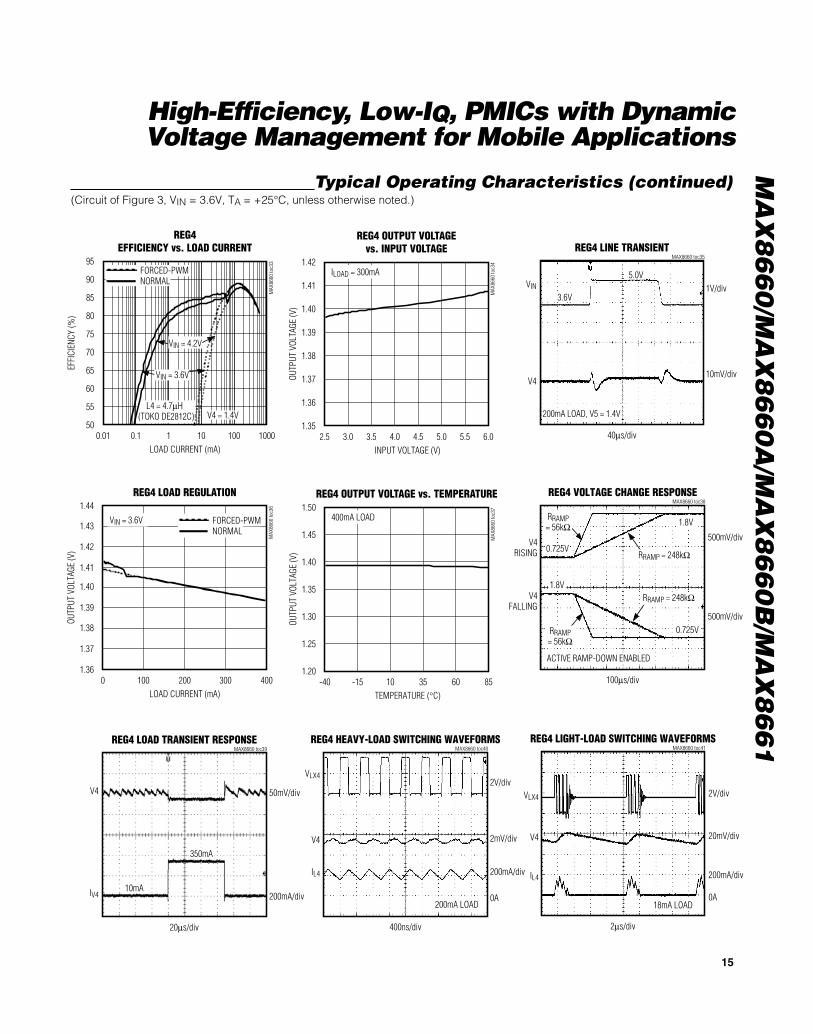
REG4EFFICIENCY vs. LOAD CURRENT
LOAD CURRENT (mA)
EFFI
CIEN
CY (%
)
MAX
8660
toc3
3
50
55
60
65
70
75
80
85
90
95
0.01 0.1 1 10 100 1000
L4 = 4.7µH(TOKO DE2812C) V4 = 1.4V
VIN = 4.2V
VIN = 3.6V
FORCED-PWMNORMAL
Typical Operating Characteristics (continued)(Circuit of Figure 3, VIN = 3.6V, TA = +25°C, unless otherwise noted.)
REG4 OUTPUT VOLTAGEvs. INPUT VOLTAGE
INPUT VOLTAGE (V)
OUTP
UT V
OLTA
GE (V
)
MAX
8660
toc3
4
2.5 3.0 3.5 4.0 4.5 5.0 5.5 6.01.35
1.36
1.37
1.38
1.39
1.40
1.41
1.42ILOAD = 300mA
REG4 LINE TRANSIENTMAX8660 toc35
1V/div
10mV/div
VIN
V4
40µs/div
200mA LOAD, V5 = 1.4V
5.0V
3.6V
REG4 HEAVY-LOAD SWITCHING WAVEFORMSMAX8660 toc40
2V/div
2mV/div
200mA/div
0A
VLX4
V4
IL4
400ns/div
200mA LOAD
REG4 LIGHT-LOAD SWITCHING WAVEFORMSMAX8660 toc41
2V/div
20mV/div
200mA/div
0A
VLX4
V4
IL4
2µs/div
18mA LOAD
REG4 LOAD REGULATION
LOAD CURRENT (mA)
OUTP
UT V
OLTA
GE (V
)
MAX
8660
toc3
6
0 100 200 300 4001.36
1.37
1.38
1.39
1.40
1.41
1.42
1.43
1.44
VIN = 3.6V FORCED-PWMNORMAL
REG4 OUTPUT VOLTAGE vs. TEMPERATURE
TEMPERATURE (°C)
OUTP
UT V
OLTA
GE (V
)
MAX
8660
toc3
7
-40 -15 10 35 60 851.20
1.25
1.30
1.35
1.40
1.45
1.50400mA LOAD
REG4 VOLTAGE CHANGE RESPONSEMAX8660 toc38
500mV/div
500mV/div
V4RISING
V4FALLING
100µs/div
ACTIVE RAMP-DOWN ENABLED
RRAMP = 56kΩ
RRAMP = 248kΩ
RRAMP = 248kΩ
RRAMP = 56kΩ
0.725V
0.725V
1.8V
1.8V
REG4 LOAD TRANSIENT RESPONSEMAX8660 toc39
50mV/div
200mA/div
V4
IV4
20µs/div
10mA
350mA

MA
X8
66
0/M
AX
86
60
A/M
AX
86
60
B/M
AX
86
61
High-Efficiency, Low-IQ, PMICs with DynamicVoltage Management for Mobile Applications
16
Typical Operating Characteristics (continued)(Circuit of Figure 3, VIN = 3.6V, TA = +25°C, unless otherwise noted.)
REG5 OUTPUT VOLTAGE vs. INPUT VOLTAGE
INPUT VOLTAGE (V)
OUTP
UT V
OLTA
GE (V
)
MAX
8660
toc4
2
2.5 3.0 3.5 4.0 4.5 5.0 5.5 6.01.77
1.78
1.79
1.80
1.81
1.82
1.83100mA LOAD
REG5 OUTPUT VOLTAGE vs. LOAD CURRENT
LOAD CURRENT (mA)
OUT
PUT
VOLT
AGE
(V)
MAX
8660
toc4
3
0 50 100 150 2001.77
1.78
1.79
1.80
1.81
1.82
1.83REG5 OUTPUT VOLTAGE vs. TEMPERATURE
TEMPERATURE (°C)
OUTP
UT V
OLTA
GE (V
)
MAX
8660
toc4
4
-40 -15 10 35 60 851.77
1.78
1.79
1.80
1.81
1.82
1.83100mA LOAD
REG5 LINE TRANSIENTMAX8660 toc45
1V/div
20mV/div
VIN
V5
40µs/div
100mA LOAD, V5 = 1.8V
3.6V
5.0V100mA LOAD
REG5 LOAD TRANSIENT RESPONSEMAX8660 toc46
100mA/div
50mV/divV5
IV5
20µs/div
100mA LOAD, V5 = 1.8V
180mA
10mA
REG5 VOLTAGE CHANGE RESPONSEMAX8660 toc47
100mV/div
V5
40µs/div
RRAMP = 56kΩ 2.0V
1.725V
REG5 OUTPUT NOISE SPECTRALDENSITY vs. FREQUENCY
FREQUENCY (kHz)
NOIS
E DE
NSIT
Y (n
V/√(
Hz))
MAX
8660
toc4
8
0.01 0.1 1 10 10010
100
1000
10,000REG5 OUTPUT NOISE (0.1Hz TO 10Hz)
MAX8660 toc49
10µV/div
1s/div
REG5 PSRR vs. FREQUENCY
FREQUENCY (kHz)
PSRR
(dB)
MAX
8660
toc5
0
0
10
20
30
40
50
60
70
80
0.01 0.1 1 10 100
RLOAD = 180Ω

MA
X8
66
0/M
AX
86
60
A/M
AX
86
60
B/M
AX
86
61
High-Efficiency, Low-IQ, PMICs with DynamicVoltage Management for Mobile Applications
17
Typical Operating Characteristics (continued)(Circuit of Figure 3, VIN = 3.6V, TA = +25°C, unless otherwise noted.)
REG6/REG7 OUTPUT VOLTAGEvs. INPUT VOLTAGE
INPUT VOLTAGE (V)
OUTP
UT V
OLTA
GE (V
)
MAX
8660
toc5
1
2.5 3.0 3.5 4.0 4.5 5.0 5.5 6.01.77
1.78
1.79
1.80
1.81
1.82
1.83100mA LOAD
REG6/REG7 OUTPUT VOLTAGEvs. LOAD CURRENT
LOAD CURRENT (mA)
OUT
PUT
VOLT
AGE
(V)
MAX
8660
toc5
2
0 100 200 300 400 500 600 700 800 9001.0
1.5
2.0
2.5
3.0
3.5
4.2V INPUT3.3V OUTPUT
2.4V INPUT1.8V OUTPUT
REG6/REG7 OUTPUT VOLTAGEvs. TEMPERATURE
TEMPERATURE (°C)
OUTP
UT V
OLTA
GE (V
)
MAX
8660
toc5
3
-40 -15 10 35 60 851.70
1.72
1.74
1.76
1.78
1.80
1.82
1.84
1.86
1.88
1.90300mA LOAD
REG6/REG7 LINE TRANSIENTMAX8660 toc54
1V/div
V6/V7
VIN
40µs/div
300mA LOAD, V6/V7 = 1.8V
20mV/div
3.6V
5.0V
REG6/REG7 LOAD TRANSIENTMAX8660 toc55
100mA/divIV6/IV7
V6/V7
10µs/div
V6/V7 = 1.8V
50mV/div
10mA
300mA
REG6/REG7 ENABLE WAVEFORMMAX8660 toc56
500mV/div
2V/divVSDA
V6/V7
100µs/div
I2C ENABLE SIGNAL
60µs
REG6/REG7 DROPOUT OUTPUT VOLTAGEvs. LOAD CURRENT
LOAD CURRENT (mA)
DRO
POUT
VOL
TAGE
(mV)
MAX
8660
toc5
7
0 100 200 300 400 5000
20
40
60
80
100
120
140
3.3V OUTPUT
3.0V OUTPUT
THE SLOPE OF THESE LINESSHOWS THAT THE REG6/REG7 DROPOUT RESISTANCE OF ANAVERAGE PART MOUNTED ON THE MAXIMEVALUATION KIT IS 205mΩ.

MA
X8
66
0/M
AX
86
60
A/M
AX
86
60
B/M
AX
86
61
High-Efficiency, Low-IQ, PMICs with DynamicVoltage Management for Mobile Applications
18
Typical Operating Characteristics (continued)(Circuit of Figure 3, VIN = 3.6V, TA = +25°C, unless otherwise noted.)
REG8 OUTPUT VOLTAGE vs. INPUT VOLTAGE
INPUT VOLTAGE (V)
OUTP
UT V
OLTA
GE (V
)
MAX
8660
toc5
8
2.5 3.0 3.5 4.0 4.5 5.0 5.5 6.02.0
2.2
2.4
2.6
2.8
3.0
3.2
3.4 5mA LOAD
REG8 LOAD REGULATION
LOAD CURRENT (mA)V8
(V)
MAX
8660
toc5
9
0 10 20 30 40 50 60 70 802.0
2.2
2.4
2.6
2.8
3.0
3.2
3.4
3.6
3.8
4.0
VIN = 3.6V
REG8 OUTPUT VOLTAGE vs. TEMPERATURE
TEMPERATURE (°C)
OUTP
UT V
OLTA
GE (V
)
MAX
8660
toc6
0
-40 -15 10 35 60 853.20
3.22
3.24
3.26
3.28
3.30
3.32
3.34
3.36
3.38
3.40
5mA LOAD
REG8 LINE TRANSIENTMAX8660 toc61
50mV/div
1V/divVIN
V8
40µs/div
10mA LOAD
3.6V
5.0V
REG8 LOAD TRANSIENTMAX8660 toc62
50mV/div
10mA/div
V8
IV8
10µs/div
5mA
15mA
REG8 DROPOUT VOLTAGE vs. LOAD CURRENT
LOAD CURRENT (mA)
DROP
OUT
VOLT
AGE
(mV)
MAX
8660
toc6
3
0 5 10 15 20 25 300
50
100
150
200
250
300
350
400THE SLOPE OF THIS LINESHOWS THAT THE REG8 DROPOUTRESISTANCE OF AN AVERAGE PART MOUNTED ON THE MAXIMEVALUATION KIT IS 12.4Ω.

MA
X8
66
0/M
AX
86
60
A/M
AX
86
60
B/M
AX
86
61
High-Efficiency, Low-IQ, PMICs with DynamicVoltage Management for Mobile Applications
19
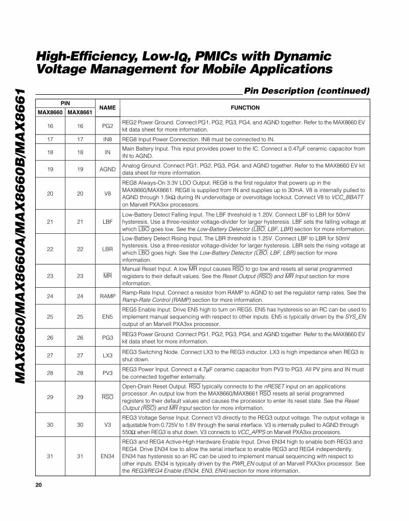
Pin Description
PIN
MAX8660 MAX8661NAME FUNCTION
1 1 IN5
REG5 Power Input. Connect IN5 to IN to ensure V5 rises first to meet the Marvell PXA3xxprocessor’s sequencing requirements. If adherence to this sequencing specification is notrequired, connect IN5 to V1, V2, or another supply between 2.35V and VIN. See the LinearRegulators (REG5–REG8) section for more information.
— 2 V5
REG5 Linear-Regulator Output. V5 defaults to 1.8V and is adjustable from 1.7V to 2.0V throughthe serial interface. The input to the V5 regulator is IN5. Use V5 to power VCC_MVT, VCC_BG,VCC_OSC13M, and VCC_PLL on Marvell PXA3xx processors. V5 is internally pulled to AGNDthrough 2kΩ when REG5 is shut down.
3 3 PV4REG4 Power Input. Connect a 4.7µF ceramic capacitor from PV4 to PG4. All PV pins and IN mustbe connected together externally.
4 4 LX4REG4 Switching Node. Connect LX4 to the REG4 inductor. LX4 is high impedance when REG4 isshut down.
5 5 PG4RE G 4 P ow er G r ound . C onnect P G 1, P G 2, P G 3, P G 4, and AG N D tog ether . Refer to the M AX 8660 E V ki t data sheet for more information.
6 6 SET2REG2 Voltage Select Input. SET2 is a tri-level logic input. Connect SET2 to select the V2 outputvoltage as detailed in Table 4. The REG2 output voltage selected by SET2 is latched at the end ofthe REG2 soft-start period. Changes to SET2 after the startup period have no effect.
7 7 V6
REG6 Linear-Regulator Output. REG6 is activated and programmed through the serial interface tooutput from 1.8V to 3.3V in 0.1V steps. REG6 is off by default. V6 is internally pulled to AGNDthrough 350Ω when REG6 is shut down. V6 optionally powers VCC_CARD1 on Marvell PXA3xxprocessors.
8 — IN67REG6 and REG7 Power Input. IN67 is typically connected to IN. IN67 can also be connected toany supply between 2.35V to VIN.
— 8 IN6REG6 Power Input. IN6 is typically connected to IN. IN6 can also be connected to any supplybetween 2.35V to VIN.
9 — V7
REG7 Linear-Regulator Output. REG7 is activated and programmed through the serial interface tooutput from 1.8V to 3.3V in 0.1V steps. REG7 is off by default. V7 is internally pulled to AGNDthrough 350Ω when REG7 is shut down. V7 optionally powers VCC_CARD2 on Marvell PXA3xxprocessors.
— 9 N.C. No Internal Connection
10 10 V2REG2 Voltage Sense Input. Connect V2 directly to the REG2 output voltage. The output voltage ofREG2 is selected by SET2. V2 is internally pulled to AGND through 650Ω when REG2 is shutdown. V2 powers VCC_MEM on Marvell PXA3xx processors.
11 11 SCL Serial-Clock Input. See the I 2C Interface section.
12 12 SDA Serial-Data Input. See the I 2C Interface section.
13 13 LBOLow-Battery Output. LBO is an open-drain output that pulls low when LBF is below its threshold.LBO typically connects to the nBATT_FAULT input of the applications processor to indicate thatthe battery has been removed or discharged.
14 14 PV2REG2 Power Input. Connect a 4.7µF ceramic capacitor from PV2 to PG2. All PV pins and IN mustbe connected together externally.
15 15 LX2REG2 Switching Node. Connect LX2 to the REG2 inductor. LX2 is high impedance when REG2 isshut down.
MA
X8
66
0/M
AX
86
60
A/M
AX
86
60
B/M
AX
86
61
High-Efficiency, Low-IQ, PMICs with DynamicVoltage Management for Mobile Applications
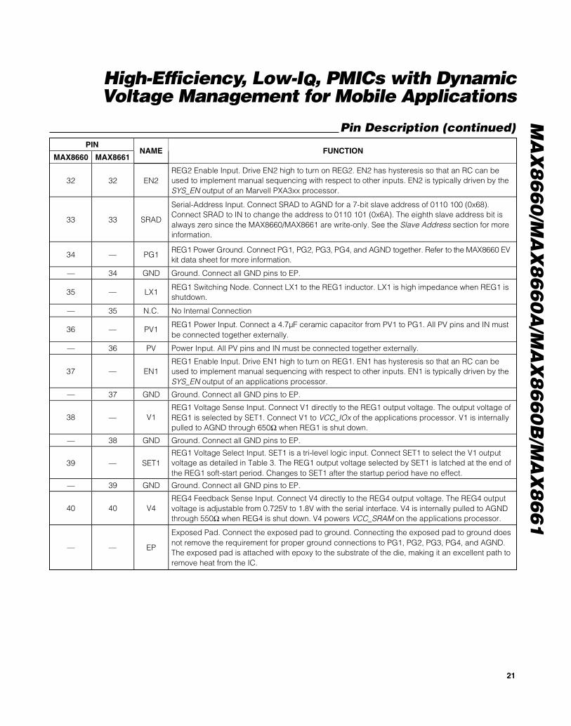
20
Pin Description (continued)PIN
MAX8660 MAX8661NAME FUNCTION
16 16 PG2RE G 2 P ow er G r ound . C onnect P G 1, P G 2, P G 3, P G 4, and AG N D tog ether . Refer to the M AX 8660 E V ki t data sheet for more information.
17 17 IN8 REG8 Input Power Connection. IN8 must be connected to IN.
18 18 INMain Battery Input. This input provides power to the IC. Connect a 0.47µF ceramic capacitor fromIN to AGND.
19 19 AGNDAnalog Ground. Connect PG1, PG2, PG3, PG4, and AGND together. Refer to the MAX8660 EV kitdata sheet for more information.
20 20 V8
REG8 Always-On 3.3V LDO Output. REG8 is the first regulator that powers up in theMAX8660/MAX8661. REG8 is supplied from IN and supplies up to 30mA. V8 is internally pulled toAGND through 1.5kΩ during IN undervoltage or overvoltage lockout. Connect V8 to VCC_BBATTon Marvell PXA3xx processors.
21 21 LBFLow-Battery Detect Falling Input. The LBF threshold is 1.20V. Connect LBF to LBR for 50mVhysteresis. Use a three-resistor voltage-divider for larger hysteresis. LBF sets the falling voltage atwhich LBO goes low. See the Low-Battery Detector (LBO, LBF, LBR) section for more information.
22 22 LBR
Low-Battery Detect Rising Input. The LBR threshold is 1.25V. Connect LBF to LBR for 50mVhysteresis. Use a three-resistor voltage-divider for larger hysteresis. LBR sets the rising voltage atwhich LBO goes high. See the Low-Battery Detector (LBO, LBF, LBR) section for moreinformation.
23 23 MRManual Reset Input. A low MR input causes RSO to go low and resets all serial programmedregisters to their default values. See the Reset Output (RSO) and MR Input section for moreinformation.
24 24 RAMPRamp-Rate Input. Connect a resistor from RAMP to AGND to set the regulator ramp rates. See theRamp-Rate Control (RAMP) section for more information.
25 25 EN5REG5 Enable Input. Drive EN5 high to turn on REG5. EN5 has hysteresis so an RC can be used toimplement manual sequencing with respect to other inputs. EN5 is typically driven by the SYS_ENoutput of an Marvell PXA3xx processor.
26 26 PG3RE G 3 P ow er G r ound . C onnect P G 1, P G 2, P G 3, P G 4, and AG N D tog ether . Refer to the M AX 8660 E V ki t data sheet for more information.
27 27 LX3REG3 Switching Node. Connect LX3 to the REG3 inductor. LX3 is high impedance when REG3 isshut down.
28 28 PV3REG3 Power Input. Connect a 4.7µF ceramic capacitor from PV3 to PG3. All PV pins and IN mustbe connected together externally.
29 29 RSO
Open-Drain Reset Output. RSO typically connects to the nRESET input on an applicationsprocessor. An output low from the MAX8660/MAX8661 RSO resets all serial programmedregisters to their default values and causes the processor to enter its reset state. See the ResetOutput (RSO) and MR Input section for more information.
30 30 V3REG3 Voltage Sense Input. Connect V3 directly to the REG3 output voltage. The output voltage i sad j ustab l e fr om 0.725V to 1.8V thr oug h the ser i al i nter face. V 3 i s i nter nal l y p ul l ed to AGN D thr oug h550Ω w hen RE G3 i s shut d ow n. V 3 connects to V C C _AP P S on M ar vel l P X A3xx p r ocessor s.
31 31 EN34
REG3 and REG4 Active-High Hardware Enable Input. Drive EN34 high to enable both REG3 andREG4. Drive EN34 low to allow the serial interface to enable REG3 and REG4 independently.EN34 has hysteresis so an RC can be used to implement manual sequencing with respect toother inputs. EN34 is typically driven by the PWR_EN output of an Marvell PXA3xx processor. Seethe REG3/REG4 Enable (EN34, EN3, EN4) section for more information.
MA
X8
66
0/M
AX
86
60
A/M
AX
86
60
B/M
AX
86
61
High-Efficiency, Low-IQ, PMICs with DynamicVoltage Management for Mobile Applications
21
Pin Description (continued)PIN
MAX8660 MAX8661NAME FUNCTION
32 32 EN2REG2 Enable Input. Drive EN2 high to turn on REG2. EN2 has hysteresis so that an RC can beused to implement manual sequencing with respect to other inputs. EN2 is typically driven by theSYS_EN output of an Marvell PXA3xx processor.
33 33 SRAD
Serial-Address Input. Connect SRAD to AGND for a 7-bit slave address of 0110 100 (0x68).Connect SRAD to IN to change the address to 0110 101 (0x6A). The eighth slave address bit isalways zero since the MAX8660/MAX8661 are write-only. See the Slave Address section for moreinformation.
34 — PG1RE G 1 P ow er G r ound . C onnect P G 1, P G 2, P G 3, P G 4, and AG N D tog ether . Refer to the M AX 8660 E V ki t data sheet for more information.
— 34 GND Ground. Connect all GND pins to EP.
35 — LX1REG1 Switching Node. Connect LX1 to the REG1 inductor. LX1 is high impedance when REG1 isshutdown.
— 35 N.C. No Internal Connection
36 — PV1REG1 Power Input. Connect a 4.7µF ceramic capacitor from PV1 to PG1. All PV pins and IN mustbe connected together externally.
— 36 PV Power Input. All PV pins and IN must be connected together externally.
37 — EN1REG1 Enable Input. Drive EN1 high to turn on REG1. EN1 has hysteresis so that an RC can beused to implement manual sequencing with respect to other inputs. EN1 is typically driven by theSYS_EN output of an applications processor.
— 37 GND Ground. Connect all GND pins to EP.
38 — V1REG1 Voltage Sense Input. Connect V1 directly to the REG1 output voltage. The output voltage ofREG1 is selected by SET1. Connect V1 to VCC_IOx of the applications processor. V1 is internallypulled to AGND through 650Ω when REG1 is shut down.
— 38 GND Ground. Connect all GND pins to EP.
39 — SET1REG1 Voltage Select Input. SET1 is a tri-level logic input. Connect SET1 to select the V1 outputvoltage as detailed in Table 3. The REG1 output voltage selected by SET1 is latched at the end ofthe REG1 soft-start period. Changes to SET1 after the startup period have no effect.
— 39 GND Ground. Connect all GND pins to EP.
40 40 V4REG4 Feedback Sense Input. Connect V4 directly to the REG4 output voltage. The REG4 outputvoltage is adjustable from 0.725V to 1.8V with the serial interface. V4 is internally pulled to AGNDthrough 550Ω when REG4 is shut down. V4 powers VCC_SRAM on the applications processor.
— — EP
Exposed Pad. Connect the exposed pad to ground. Connecting the exposed pad to ground doesnot remove the requirement for proper ground connections to PG1, PG2, PG3, PG4, and AGND.The exposed pad is attached with epoxy to the substrate of the die, making it an excellent path toremove heat from the IC.

MA
X8
66
0/M
AX
86
60
A/M
AX
86
60
B/M
AX
86
61
High-Efficiency, Low-IQ, PMICs with DynamicVoltage Management for Mobile Applications
22
AUXILIARY POWER
AUXILIARY POWER
SD/CF MEMORYCARD 1
SD/CF MEMORYCARD 2
SYS_EN
PWR_EN
nRESET
nBATT_FAULT
SDA GPIO33
SCL GPIO32
PWR_SDAPWR_SCL
LBO
IN
V1
I2C
RSO
EN1
EN2
EN5
EN34
VCC_I01
VCC_I03
VCC_I04
VCC_I06
VCC_LCD
VCC_MSL
VCC_DF
VCC_CI
VCC_MEM
VCC_APPS
VCC_SRAM
VCC_MVT
VCC_BG
VCC_PLL
VCC_OSC13M
VCC_CARD1
VCC_CARD2
VCC_BBATT
VCC_USB
VCC_TSIMARVELL PXA3xx
PROCESSOR
V8 (VCC_BBATT)
MAX8660
AUXILIARY POWERPERIPHERALS
AUXILARY POWERPERIPHERALS MEMORY
3.3V AT 1200mA
1.8V AT 900mA
3.3V AT 30mA
0.725V TO 1.8V AT 1600mA
0.725V TO 1.8V AT 400mA
1.7V TO 2.0V (DEF 1.8V) AT 200mA
1.8V TO 3.3V (DEF 0V) AT 500mA
1.8V TO 3.3V (DEF 0V) AT 500mA
V2
V3
V4
V5
V6
V7
V8
1045mA
135mA
160mA
540mA
40mA
485mA
485mA
25mA
STANDARD I2C
POWER I2C
15mA
10mA
25mA
50mA
50mA
55mA
20mA
50mA
35mA
200mA
1600mA
360mA
15mA
15mA
5mA
5mA
Figure 1. Example MAX8660 Connection to Marvell PXA3xx Processor. This is one example only. Other connections are also supported.

MA
X8
66
0/M
AX
86
60
A/M
AX
86
60
B/M
AX
86
61
High-Efficiency, Low-IQ, PMICs with DynamicVoltage Management for Mobile Applications
23
MAX8660MAX8661
IN
EN1EN2
IN8TO IN
V8
V6
IN67 (IN6)
V7
SCL
SDA
SRAD
VCC_IOx
RSO
FROM CPUSYS_EN
( ) ARE FOR THE MAX8661
RAMP
LBR(1.25V)
LBO
LBF(1.20V)
BATT
V1
SET1
PV1
PWMON
STEP-DOWNPWMREG1
PG1
LX1
TO BATT
V1,VCC_I0x, VCC_LCD,VCC_MSL, VDD_USB,VCC_DF, VDD_CI, VCC_TSIMAX8660/MAX8660B: 3.3V, 3.0V, 2.85VMAX8660A: 2.5V, 2.0V, 1.8V1200mA
(MAX8660/MAX8660A/MAX8660B ONLY)
LATCH
V2
SET2
PV2
PWM
ON
STEP-DOWNPWMREG2
PG2
LX2
TO BATT
V2,VCC_MEMMAX8660/MAX8660B/MAX8661: 3.3V, 2.5V, 1.8VMAX8660A: 2.5V, 2.0V, 1.8V900mA
LATCH
V3
EN34
PV3
PWM
RAMP
ON
STEP-DOWNPWMREG3
PG3
LX3
TO BATT
FROM CPUPWR_EN
V3,VCC_APPS0.725V TO 1.8V(DEFAULT 1.4V for MAX8660/MAX8660A/MAX8661)(DEFAULT 1.15V for MAX8660B)1.6A
ADJ0.725V TO1.8V
V4
IN5
V5
EN5
PV4
PWM
RAMP
STEP-DOWNPWMREG4
PG4
LX4
TO BATT
TO IN, V1 OR V2
V4,VCC_SRAM0.725V TO 1.8V(DEFAULT 1.4V for MAX8660/MAX8660A/MAX8661)(DEFAULT 1.15V for MAX8660B)400mA
RAMP
ADJ1.7V TO2.0V
ADJ0.725V TO1.8V
OPEN-DRAIN LOW BATT OUTTO nBATT_FAULT
BATTERY
AGND
UVLOOVLOANDBATTMON
REF1.25V
TO ALLBLOCKS
V8,VCC_BBATT
(3.3V 30mA, ALWAYS ON)
V6,VCC_CARD10V/1.8–3.3V
(DEFAULT 0V) 500mA
V7,VCC_CARD20V/1.8–3.3V
(DEFAULT 0V) 500mA(MAX8660/MAX8660A ONLY)
RESETV8 < 2.4V
20ms
SET RATERAMP
MRHARDWARERESET INPUT
TO CPUnRESET
LDOREG8
LDOREG7
LDOREG6
TO V1, V2, OR IN
V5,VCC_MVT, VCC_BG1.7V TO 2.0V(DEFAULT 1.8V)200mA
LDOREG5
FROM CPUSYS_EN
EP
AGND PGND
I2C SERIALINTERFACE
LOGICAL OR(FIGURE 5)
Figure 2. Functional Diagram
MA
X8
66
0/M
AX
86
60
A/M
AX
86
60
B/M
AX
86
61
High-Efficiency, Low-IQ, PMICs with DynamicVoltage Management for Mobile Applications
24
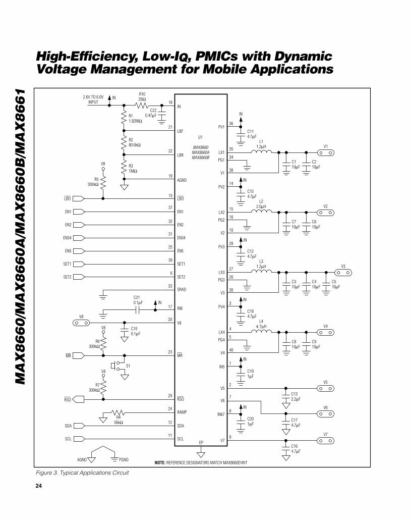
Figure 3. Typical Applications Circuit
U1
MAX8660MAX8660AMAX8660B
V8
V1
IN
35
34LX1
PG1
38V1
36PV1
C210µF
C110µF
C114.7µF
C220.47µF
L11.2µH
V2
IN
15
16LX2
PG2
10V2
14PV2
C610µF
C710µF
C154.7µF
L22.0µH
V3
IN
27
26LX3
PG3
30V3
28PV3
C410µF
C510µF
C310µF
C124.7µF
L31.2µH
V4
IN
4
5LX4
PG4
40V4
3PV4
C910µF
C810µF
C184.7µF
L44.7µH
V5
IN
2V5
1IN5
C132.2µF
V79V7
C164.7µF
V6
7V6
C174.7µF
C191µF
C100.1µF
R6300kΩ
C210.1µF
IN8
11
IN67
SCL
AGND PGND
SCL
C201µF
EP
NOTE: REFERENCE DESIGNATORS MATCH MAX8660EVKIT
12SDA SDA
20V8
6SET2 SET2
39SET1 SET1
25EN5 EN5
31
32
37
EN34 EN34
EN2 EN2
EN1 EN1
18IN
21LBF
22LBR
19AGND
13LBO LBO
24RAMP
R456kΩ
33SRAD
17 IN8
29RSO RSO
23MR MR
R5300kΩ
V8
V8
IN
IN
R31MΩ
R280.6kΩ
R11.82MΩ
R1020Ω2.6V TO 6.0V
INPUT
R7300kΩ
V8S1

MA
X8
66
0/M
AX
86
60
A/M
AX
86
60
B/M
AX
86
61
High-Efficiency, Low-IQ, PMICs with DynamicVoltage Management for Mobile Applications
25
Detailed DescriptionThe MAX8660/MAX8661 PMICs are optimized fordevices using the applications processors, includingsmart cellular phones, PDAs, Internet appliances, andother portable devices requiring substantial computingand multimedia capability and low power consumption.The MAX8660/MAX8661 comply with the specificationsfor Marvell’s PXA300 family (PXA3xx) and Marvell’sArmada 100 family (PXA16x) of processors.
As shown in Figure 2, the MAX8660 integrates eighthigh-performance, low-operating-current power sup-plies. REG1–REG4 are step-down DC-DC converters,and REG5–REG8 are linear regulators. Other functionsinclude low-battery detection (LBO), a reset output(RSO), a manual reset input (MR), and a 2-wire I2C seri-al interface. The MAX8661 functions the same as theMAX8660, but does not have the REG1 step-down reg-ulator and the REG7 linear regulator.
The operating input voltage range is from 2.6V to 6.0V,allowing use with a 1-cell Li+ battery, 3-cell NiMH, or a5V input. Input protection is provided with undervoltageand overvoltage lockouts. Overvoltage lockout protectsthe device against inputs up to 7.5V.
Maxim vs. Marvell PXA3xx TerminologyThe MAX8660/MAX8661 are compatible with Marvell‘sPXA3xx processor. Figure 1 shows one of many possi-ble connections between the PXA3xx processor andthe MAX8660/MAX8661. To facilitate system develop-ment with PXA3xx processors, this document uses bothMaxim and Marvell terminology. Marvell terminologyappears in parentheses and italics. For example, thisdocument refers to “V8 (VCC_BBATT)” because theMAX8660 V8 output powers the Marvell VCC_BBATTpower domain. Tables 1 and 2 outline Maxim andMarvell terminology.
POWER DOMAINPOWER DOMAIN
ACCEPTABLE VOLTAGECOMPATIBLE MAXIM
POWER DOMAINDESCRIPTION
VCC_IO1VCC_IO3VCC_IO4VCC_IO6
1.8V ±10% or3.0V ±10% or
3.3V ±10%V1 or V2
• Peripheral I/O supply for UARTs, standard I2C,power I2C, audio interface, SSPs, PWMs, etc.(VCC_IO1,VCC_IO3, VCC_IO4, VCC_IO6)
VCC_LCDVCC_MSLVCC_CIVCC_DF
1.8V ±10% or3.0V ±10%
V1 or V2
• LCD interface logic (VCC_LCD)• Fast serial interface (VCC_MSL)• Camera flash interface (VCC_CI)• Data flash interface (VCC_DF)
VCC_MEM 1.8V ±100mV V2 • I/O supply for high-speed memory
VCC_APPS 0.95V to 1.41V ±5% V3 • Main processor core
VCC_SRAM1.08V to 1.41V
±100mVV4 • Internal SRAM memory
VCC_MVTVCC_BG
VCC_OSC13MVCC_PLL
1.8V±100mV
V5
• Internal logic and I/O blocks (VCC_MVT)• Bandgap reference (VCC_BG)• 13MHz oscillator (VCC_OSC13M)• Phase-locked loop (PLL) and oscillator (VCC_PLL)
VCC_CARD11.8V ±10% or3.0V ±10% or
3.3V ±10%V6 • Removable storage and USIM card supply
VCC_CARD21.8V ±10% or3.0V ±10% or
3.3V ±10%V7 • Removable storage and USIM card supply
VCC_BBATT 3.0V ±1V V8 • Regulated battery voltage
VCC_USB 3.3V ±300mVV1 or V2
(if programmed to 3.3V)• Universal serial bus (VCC_USB)
VCC_TSI 3.3V ±300mVV1 or V2
(if programmed to 3.3V)• Touch-screen interface (VCC_TSI)
Table 1. Maxim and Marvell PXA3xx Power Domain Terminology

MA
X8
66
0/M
AX
86
60
A/M
AX
86
60
B/M
AX
86
61
High-Efficiency, Low-IQ, PMICs with DynamicVoltage Management for Mobile Applications
26
MAXIM MARVELL DESCRIPTION
EN34 PWR_ENActive-High Enable Signal for Processor Core Power. The applications processor drives thisPWR_EN signal high to exit sleep mode. The processor’s PWR_EN logic is powered by theMAX8660/MAX8661 “always on” V8 (VCC_BBATT) regulator during sleep mode.
EN1, EN2, EN5 SYS_ENActive-High Enable Signal for Peripheral Power Supplies. The applications processor drivesthis SYS_EN signal high to enter run mode.
RSO nRESETActive-Low Reset. The MAX8660/MAX8661 drive this signal low to reset the processor.When RSO goes low, the MAX8660/MAX8661 I2C registers are reset to their default values.
LBO nBATT_FAULTActive-Low Battery Fault. The MAX8660/MAX8661 drive this signal low to signal theprocessor that the battery has been removed or discharged.
SDAGPIO33
PWR_SDA
I2C Serial-Data Input/Output. The MAX8660/MAX8861 SDA generally connects to both theMarvell PXA3xx processor’s standard I2C data line (GPIO33) and its dedicated power I2Cdata line. This connection operates as an I2C multimaster system with theMAX8660/MAX8661 accepting commands from both the standard I2C and the power I2C.
SCLGPIO32
PWR_SCL
I2C Serial Clock. The MAX8660/MAX8661 SCL generally connects to both the MarvellPXA3xx processor’s standard I2C clock line (GPIO32) and its dedicated power I2C clockline. This connection operates as an I2C multimaster system with the MAX8660/MAX8661accepting commands from both the standard I2C and the power I2C.
Table 2. Maxim and Marvell PXA3xx Digital Signal Terminology
Step-Down DC-DC Converters(REG1–REG4)
REG1 (VCC_IO) Step-Down DC-DC Converter(MAX8660 Only)
REG1 is a high-efficiency (REG1 + REG8 IQ = 40µA)2MHz current-mode step-down converter that outputsup to 1200mA with efficiency up to 96% (see theTypical Operating Characteristics). The output voltage(V1) is selected with the SET1 input as shown in Table3. The REG1 output voltage selection is latched at theend of the REG1 soft-start period. Changes in SET1after the startup period have no effect.
EN1 is a dedicated enable input for REG1. Drive EN1high to enable REG1 or drive EN1 low to disable REG1.EN1 has hysteresis so that an RC may be used toimplement manual sequencing with respect to otherinputs. In systems based on Marvell PXA3xx proces-sors, EN1, EN2, and EN5 are typically connected toSYS_EN (Table 2).
The REG1 step-down regulator operates in either nor-mal or forced-PWM mode. See the REG1–REG4 Step-Down DC-DC Converter Operating Modes section formore information.
REG1 has an on-chip synchronous rectifier. See theREG1–REG4 Synchronous Rectification section formore information.
The REG1 regulator allows 100% duty-cycle operation.See the REG1/REG2 100% Duty-Cycle Operation(Dropout) section for more information.
REG2 (VCC_IO, VCC_MEM) Step-Down DC-DC Converters
REG2 is a high-efficiency (REG2 + REG8 IQ = 40µA)2MHz current-mode step-down DC-DC converter thatoutputs up to 900mA with efficiency up to 96%. The out-put voltage is selected with the SET2 input as shown inTable 4. The REG2 output voltage selection is latchedat the end of the REG2 soft-start period. Changes inSET2 after the startup period have no effect.
SET1*MAX8660/
MAX8660B: V1 (V)MAX8660A: V1 (V)
IN 3.3 2.5
UNCONNECTED 3.0 2.0
GROUND 2.85 1.8
Table 3. SET1 Logic
*SET1 is latched after REG1 startup.
SET2*M A X8 6 6 0 /M A X8 6 6 0 B /
M A X8 6 6 1 : V2 ( V) M A X8 6 6 0 A : V2 ( V)
IN 3.3 2.5
UNCONNECTED 2.5 2.0
GROUND 1.8 1.8
Table 4. SET2 Logic
*SET2 is latched after REG2 startup.

MA
X8
66
0/M
AX
86
60
A/M
AX
86
60
B/M
AX
86
61
High-Efficiency, Low-IQ, PMICs with DynamicVoltage Management for Mobile Applications
27
EN2 is a dedicated enable input for REG2. Drive EN2high to enable REG2 or drive EN2 low to disable REG2.EN2 has hysteresis so that an RC may be used toimplement manual sequencing with respect to otherinputs. In systems based on Marvell PXA3xx, EN1,EN2, and EN5 are typically connected to SYS_EN(Table 2).
The REG2 step-down regulator operates in either nor-mal or forced-PWM mode. See the REG1–REG4 Step-Down DC-DC Converter Operating Modes section formore information.
The REG2 regulator has an on-chip synchronous rectifier.See the REG1–REG4 Synchronous Rectification sectionfor more information.
The REG2 regulator allows 100% duty-cycle operation.See the REG1/REG2 100% Duty-Cycle Operation(Dropout) section for more information.
REG3 (VCC_APPS) Step-Down DC-DC ConvertersREG3 is a high-efficiency (REG3 + REG8 IQ = 45µA)2MHz current-mode step-down converter that has anI2C-adjustable output voltage from 0.725V to 1.800V in25mV increments with efficiency up to 92%. The defaultREG3 output voltage is 1.4V for the MAX8660/MAX8660A/MAX8661, and 1.15V for the MAX8660B(contact factory for other default voltages). REG3 deliv-ers up to 1.6A. See the I2C Interface section for detailson how to adjust the output voltage.
REG3 has an I2C enable bit (EN3) and a shared hard-ware enable pin (EN34). See the REG3/REG4 Enable(EN34, EN3, EN4) section for more information.
The REG3 step-down regulator operates in either nor-mal or forced-PWM mode. See the REG1–REG4 Step-Down DC-DC Converter Operating Modes section formore information.
The REG3 regulator has an on-chip synchronous rectifier.See the REG1–REG4 Synchronous Rectification sectionfor more information.
REG4 (VCC_SRAM) Step-Down DC-DC ConvertersREG4 is a high-efficiency (REG4 + REG8 IQ = 45µA)2MHz current-mode step-down converter that has anI2C-adjustable output voltage from 0.725V to 1.800V in25mV increments with efficiency up to 92%. The defaultREG4 output voltage is 1.4V for the MAX8660/MAX8660A/MAX8661, and 1.15V for the MAX8660B(contact factory for other default voltages). REG4 deliv-ers up to 400mA. See the I2C Interface section fordetails on how to adjust the output voltage.
REG4 has an I2C enable bit (EN4) and a shared hard-ware enable pin (EN34). See the REG3/REG4 Enable(EN34, EN3, EN4) section for more information.
The REG4 step-down regulator operates in either nor-mal or forced-PWM mode. See the REG1–REG4 Step-Down DC-DC Converter Operating Modes section formore information.
The REG4 regulator has an on-chip synchronous rectifier.See the REG1–REG4 Synchronous Rectification sectionfor more information.
REG1–REG4 Step-DownDC-DC Converter Operating Modes
REG1–REG4 independently operate in one of twomodes: normal or forced PWM. At power-up or after areset, REG1–REG4 default to normal operation. Activateforced-PWM mode by setting bits in the FPWM register(Table 9) with the I2C interface. The FPWM bits can bechanged at any time.
In forced-PWM mode, a converter operates with a con-stant 2MHz switching frequency regardless of outputload. The MAX8660/MAX8661 regulate the output volt-age by modulating the switching duty cycle. Forced-PWM mode is ideal for low-noise systems becauseoutput voltage ripple is small (< 10mVP-P) and switch-ing harmonics occur at multiples of the constant-switching frequency and are easily filtered. However,light-load power consumption in forced-PWM mode ishigher than that of normal mode (Table 7).
Normal operation offers improved efficiency at lightloads by switching only as necessary to supply theload. With moderate to heavy loading, the regulatorswitches at a fixed 2MHz switching frequency as itdoes in forced-PWM mode. This transition to fixed-fre-quency switching occurs at the load current specifiedin the following equation:
REG1–REG4 Synchronous RectificationInternal n-channel synchronous rectifiers eliminate theneed for external Schottky diodes and improve efficiency.The synchronous rectifier turns on during the secondhalf of each switching cycle (off-time). During this time,the voltage across the inductor is reversed, and theinductor current ramps down. In PWM mode, the syn-chronous rectifier turns off at the end of the switchingcycle. In normal mode, the synchronous rectifier turnsoff when the inductor current falls below 25mA or at theend of the switching cycle, whichever occurs first.
REG1/REG2 100% Duty-Cycle Operation (Dropout)The REG1 and REG2 step-down DC-DC convertersoperate with 100% duty cycle when the supply voltageapproaches the output voltage. This allows these
IV V
x Lx
VV x fOUT
IN OUT OUT
IN SW≅
−2
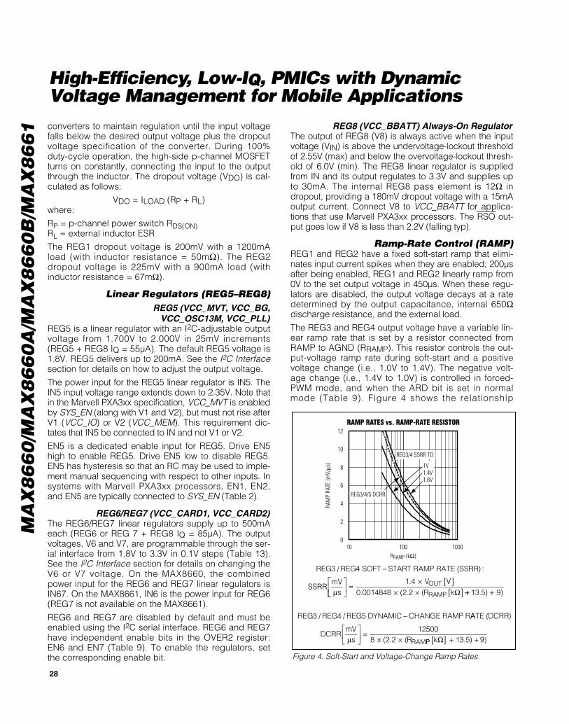
MA
X8
66
0/M
AX
86
60
A/M
AX
86
60
B/M
AX
86
61
High-Efficiency, Low-IQ, PMICs with DynamicVoltage Management for Mobile Applications
28
converters to maintain regulation until the input voltagefalls below the desired output voltage plus the dropoutvoltage specification of the converter. During 100%duty-cycle operation, the high-side p-channel MOSFETturns on constantly, connecting the input to the outputthrough the inductor. The dropout voltage (VDO) is cal-culated as follows:
VDO = ILOAD (RP + RL)where:
RP = p-channel power switch RDS(ON)RL = external inductor ESR
The REG1 dropout voltage is 200mV with a 1200mAload (with inductor resistance = 50mΩ). The REG2dropout voltage is 225mV with a 900mA load (withinductor resistance = 67mΩ).
Linear Regulators (REG5–REG8)REG5 (VCC_MVT, VCC_BG,
VCC_OSC13M, VCC_PLL)REG5 is a linear regulator with an I2C-adjustable outputvoltage from 1.700V to 2.000V in 25mV increments(REG5 + REG8 IQ = 55µA). The default REG5 voltage is1.8V. REG5 delivers up to 200mA. See the I2C Interfacesection for details on how to adjust the output voltage.
The power input for the REG5 linear regulator is IN5. TheIN5 input voltage range extends down to 2.35V. Note thatin the Marvell PXA3xx specification, VCC_MVT is enabledby SYS_EN (along with V1 and V2), but must not rise afterV1 (VCC_IO) or V2 (VCC_MEM). This requirement dic-tates that IN5 be connected to IN and not V1 or V2.
EN5 is a dedicated enable input for REG5. Drive EN5high to enable REG5. Drive EN5 low to disable REG5.EN5 has hysteresis so that an RC may be used to imple-ment manual sequencing with respect to other inputs. Insystems with Marvell PXA3xx processors, EN1, EN2,and EN5 are typically connected to SYS_EN (Table 2).
REG6/REG7 (VCC_CARD1, VCC_CARD2)The REG6/REG7 linear regulators supply up to 500mAeach (REG6 or REG 7 + REG8 IQ = 85µA). The outputvoltages, V6 and V7, are programmable through the ser-ial interface from 1.8V to 3.3V in 0.1V steps (Table 13).See the I2C Interface section for details on changing theV6 or V7 voltage. On the MAX8660, the combinedpower input for the REG6 and REG7 linear regulators isIN67. On the MAX8661, IN6 is the power input for REG6(REG7 is not available on the MAX8661).
REG6 and REG7 are disabled by default and must beenabled using the I2C serial interface. REG6 and REG7have independent enable bits in the OVER2 register:EN6 and EN7 (Table 9). To enable the regulators, setthe corresponding enable bit.
REG8 (VCC_BBATT) Always-On RegulatorThe output of REG8 (V8) is always active when the inputvoltage (VIN) is above the undervoltage-lockout thresholdof 2.55V (max) and below the overvoltage-lockout thresh-old of 6.0V (min). The REG8 linear regulator is suppliedfrom IN and its output regulates to 3.3V and supplies upto 30mA. The internal REG8 pass element is 12Ω indropout, providing a 180mV dropout voltage with a 15mAoutput current. Connect V8 to VCC_BBATT for applica-tions that use Marvell PXA3xx processors. The RSO out-put goes low if V8 is less than 2.2V (falling typ).
Ramp-Rate Control (RAMP)REG1 and REG2 have a fixed soft-start ramp that elimi-nates input current spikes when they are enabled; 200µsafter being enabled, REG1 and REG2 linearly ramp from0V to the set output voltage in 450µs. When these regu-lators are disabled, the output voltage decays at a ratedetermined by the output capacitance, internal 650Ωdischarge resistance, and the external load.
The REG3 and REG4 output voltage have a variable lin-ear ramp rate that is set by a resistor connected fromRAMP to AGND (RRAMP). This resistor controls the out-put-voltage ramp rate during soft-start and a positivevoltage change (i.e., 1.0V to 1.4V). The negative volt-age change (i.e., 1.4V to 1.0V) is controlled in forced-PWM mode, and when the ARD bit is set in normalmode (Table 9). Figure 4 shows the relationship
RAMP RATES vs. RAMP-RATE RESISTOR
RRAMP (kΩ)
RAM
P RA
TE (m
V/µs
)
0
2
4
6
8
10
12
10 100 1000
REG3/4/5 DCRR
REG3/4 SSRR TO:
1V1.4V1.8V
Figure 4. Soft-Start and Voltage-Change Ramp Rates
REG REG SOFT START RAMP RATE SSRR
SSRRmV
s
3 4/ ( ) :−
⎡µ⎣⎣
⎢⎤⎦⎥ =
× [ ]× × Ω[ ]
1 40 0014848 2 2
.. ( . (
V VR k
OUT
RAMP ++ +
−
13 5 9
3 4 5
. ) )
/ /REG REG REG DYNAMIC CHANGE RAMP RAATE DCRR
DCRRmV
s x RRAM
( )
( . (µ⎡⎣⎢
⎤⎦⎥ =
×12500
8 2 2 PP kΩ[ ] + +13 5 9. ) )
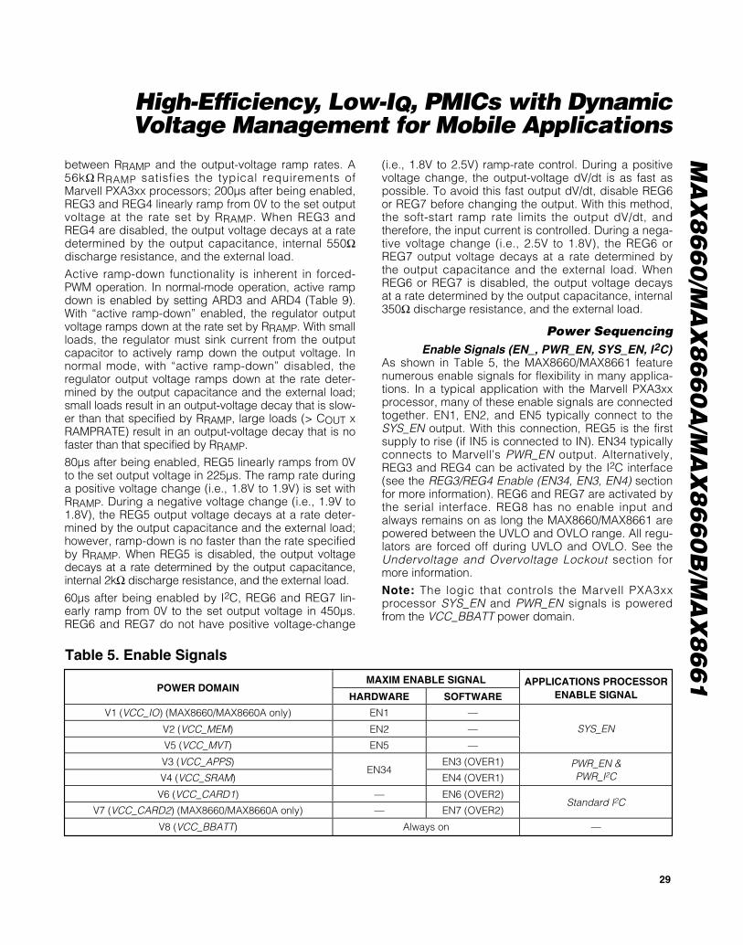
MA
X8
66
0/M
AX
86
60
A/M
AX
86
60
B/M
AX
86
61
High-Efficiency, Low-IQ, PMICs with DynamicVoltage Management for Mobile Applications
29
Table 5. Enable Signals
MAXIM ENABLE SIGNALPOWER DOMAIN
HARDWARE SOFTWAREAPPLICATIONS PROCESSOR
ENABLE SIGNAL
V1 (VCC_IO) (MAX8660/MAX8660A only) EN1 —
V2 (VCC_MEM) EN2 —
V5 (VCC_MVT) EN5 —
SYS_EN
V3 (VCC_APPS) EN3 (OVER1)
V4 (VCC_SRAM)EN34
EN4 (OVER1)PWR_EN &PWR_I2C
V6 (VCC_CARD1) — EN6 (OVER2)
V7 (VCC_CARD2) (MAX8660/MAX8660A only) — EN7 (OVER2)Standard I2C
V8 (VCC_BBATT) Always on —
between RRAMP and the output-voltage ramp rates. A56kΩ RRAMP satisfies the typical requirements ofMarvell PXA3xx processors; 200µs after being enabled,REG3 and REG4 linearly ramp from 0V to the set outputvoltage at the rate set by RRAMP. When REG3 andREG4 are disabled, the output voltage decays at a ratedetermined by the output capacitance, internal 550Ωdischarge resistance, and the external load.
Active ramp-down functionality is inherent in forced-PWM operation. In normal-mode operation, active rampdown is enabled by setting ARD3 and ARD4 (Table 9).With “active ramp-down” enabled, the regulator outputvoltage ramps down at the rate set by RRAMP. With smallloads, the regulator must sink current from the outputcapacitor to actively ramp down the output voltage. Innormal mode, with “active ramp-down” disabled, theregulator output voltage ramps down at the rate deter-mined by the output capacitance and the external load;small loads result in an output-voltage decay that is slow-er than that specified by RRAMP, large loads (> COUT xRAMPRATE) result in an output-voltage decay that is nofaster than that specified by RRAMP.
80µs after being enabled, REG5 linearly ramps from 0Vto the set output voltage in 225µs. The ramp rate duringa positive voltage change (i.e., 1.8V to 1.9V) is set withRRAMP. During a negative voltage change (i.e., 1.9V to1.8V), the REG5 output voltage decays at a rate deter-mined by the output capacitance and the external load;however, ramp-down is no faster than the rate specifiedby RRAMP. When REG5 is disabled, the output voltagedecays at a rate determined by the output capacitance,internal 2kΩ discharge resistance, and the external load.
60µs after being enabled by I2C, REG6 and REG7 lin-early ramp from 0V to the set output voltage in 450µs.REG6 and REG7 do not have positive voltage-change
(i.e., 1.8V to 2.5V) ramp-rate control. During a positivevoltage change, the output-voltage dV/dt is as fast aspossible. To avoid this fast output dV/dt, disable REG6or REG7 before changing the output. With this method,the soft-start ramp rate limits the output dV/dt, andtherefore, the input current is controlled. During a nega-tive voltage change (i.e., 2.5V to 1.8V), the REG6 orREG7 output voltage decays at a rate determined bythe output capacitance and the external load. WhenREG6 or REG7 is disabled, the output voltage decaysat a rate determined by the output capacitance, internal350Ω discharge resistance, and the external load.
Power SequencingEnable Signals (EN_, PWR_EN, SYS_EN, I2C)
As shown in Table 5, the MAX8660/MAX8661 featurenumerous enable signals for flexibility in many applica-tions. In a typical application with the Marvell PXA3xxprocessor, many of these enable signals are connectedtogether. EN1, EN2, and EN5 typically connect to theSYS_EN output. With this connection, REG5 is the firstsupply to rise (if IN5 is connected to IN). EN34 typicallyconnects to Marvell’s PWR_EN output. Alternatively,REG3 and REG4 can be activated by the I2C interface(see the REG3/REG4 Enable (EN34, EN3, EN4) sectionfor more information). REG6 and REG7 are activated bythe serial interface. REG8 has no enable input andalways remains on as long the MAX8660/MAX8661 arepowered between the UVLO and OVLO range. All regu-lators are forced off during UVLO and OVLO. See theUndervoltage and Overvoltage Lockout section formore information.
Note: The logic that controls the Marvell PXA3xxprocessor SYS_EN and PWR_EN signals is poweredfrom the VCC_BBATT power domain.
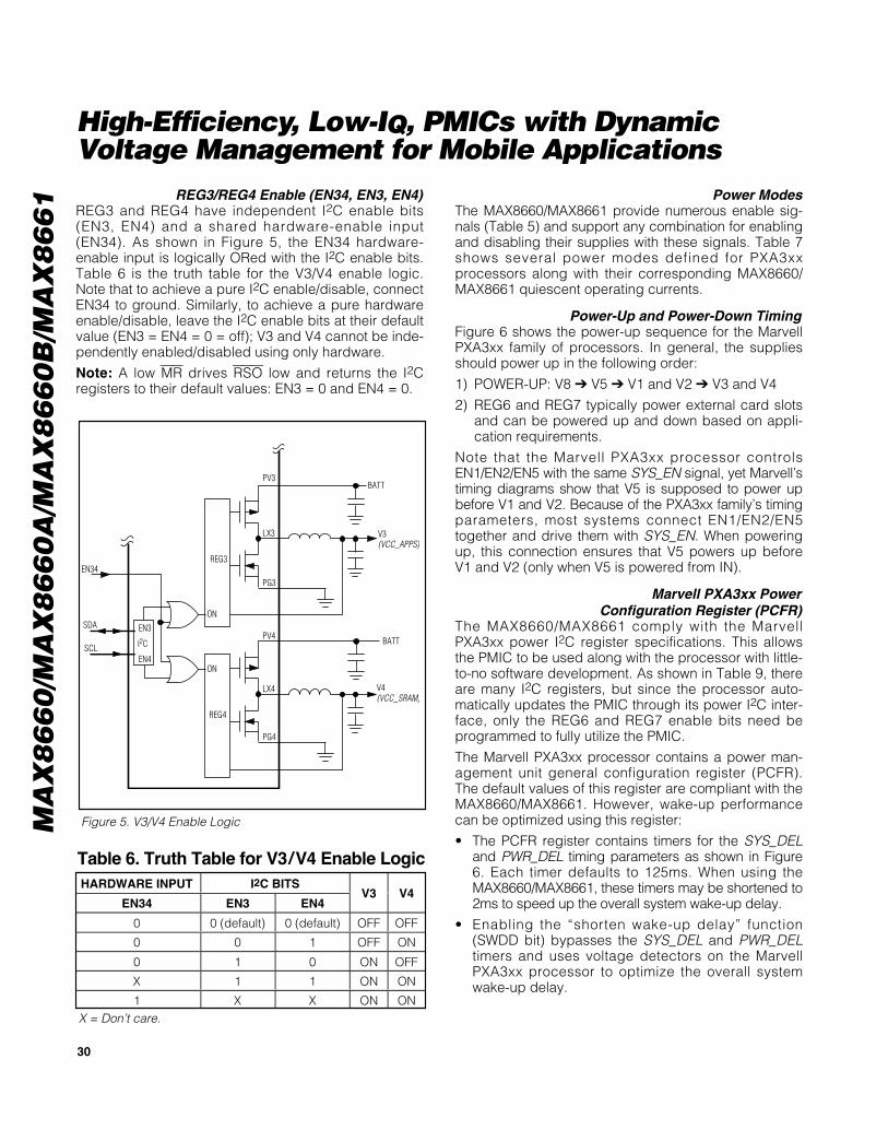
MA
X8
66
0/M
AX
86
60
A/M
AX
86
60
B/M
AX
86
61
High-Efficiency, Low-IQ, PMICs with DynamicVoltage Management for Mobile Applications
30
REG3/REG4 Enable (EN34, EN3, EN4)REG3 and REG4 have independent I2C enable bits(EN3, EN4) and a shared hardware-enable input(EN34). As shown in Figure 5, the EN34 hardware-enable input is logically ORed with the I2C enable bits.Table 6 is the truth table for the V3/V4 enable logic.Note that to achieve a pure I2C enable/disable, connectEN34 to ground. Similarly, to achieve a pure hardwareenable/disable, leave the I2C enable bits at their defaultvalue (EN3 = EN4 = 0 = off); V3 and V4 cannot be inde-pendently enabled/disabled using only hardware.
Note: A low MR drives RSO low and returns the I2Cregisters to their default values: EN3 = 0 and EN4 = 0.
Power ModesThe MAX8660/MAX8661 provide numerous enable sig-nals (Table 5) and support any combination for enablingand disabling their supplies with these signals. Table 7shows several power modes defined for PXA3xxprocessors along with their corresponding MAX8660/MAX8661 quiescent operating currents.
Power-Up and Power-Down TimingFigure 6 shows the power-up sequence for the MarvellPXA3xx family of processors. In general, the suppliesshould power up in the following order:
1) POWER-UP: V8 V5 V1 and V2 V3 and V4
2) REG6 and REG7 typically power external card slotsand can be powered up and down based on appli-cation requirements.
Note that the Marvell PXA3xx processor controlsEN1/EN2/EN5 with the same SYS_EN signal, yet Marvell’stiming diagrams show that V5 is supposed to power upbefore V1 and V2. Because of the PXA3xx family’s timingparameters, most systems connect EN1/EN2/EN5together and drive them with SYS_EN. When poweringup, this connection ensures that V5 powers up beforeV1 and V2 (only when V5 is powered from IN).
Marvell PXA3xx PowerConfiguration Register (PCFR)
The MAX8660/MAX8661 comply with the MarvellPXA3xx power I2C register specifications. This allowsthe PMIC to be used along with the processor with little-to-no software development. As shown in Table 9, thereare many I2C registers, but since the processor auto-matically updates the PMIC through its power I2C inter-face, only the REG6 and REG7 enable bits need beprogrammed to fully utilize the PMIC.
The Marvell PXA3xx processor contains a power man-agement unit general configuration register (PCFR).The default values of this register are compliant with theMAX8660/MAX8661. However, wake-up performancecan be optimized using this register:
• The PCFR register contains timers for the SYS_DELand PWR_DEL timing parameters as shown in Figure6. Each timer defaults to 125ms. When using theMAX8660/MAX8661, these timers may be shortened to2ms to speed up the overall system wake-up delay.
• Enabling the “shorten wake-up delay” function(SWDD bit) bypasses the SYS_DEL and PWR_DELtimers and uses voltage detectors on the MarvellPXA3xx processor to optimize the overall systemwake-up delay.
Figure 5. V3/V4 Enable Logic
EN34
SDA
SCLPV4
PV3
ON
REG4
PG4
LX4
EN3
EN4
BATT
V4 (VCC_SRAM)
ON
REG3
I2C
PG3
LX3
BATT
V3 (VCC_APPS)
Table 6. Truth Table for V3/V4 Enable LogicHARDWARE INPUT I2C BITS
EN34 EN3 EN4V3 V4
0 0 (default) 0 (default) OFF OFF
0 0 1 OFF ON
0 1 0 ON OFF
X 1 1 ON ON
1 X X ON ONX = Don’t care.

MA
X8
66
0/M
AX
86
60
A/M
AX
86
60
B/M
AX
86
61
High-Efficiency, Low-IQ, PMICs with DynamicVoltage Management for Mobile Applications
31
MAX8660 QUIESCENTOPERATING CURRENT (FIGURE 3)POWER
MODE
POWERDOMAINSTATE
DIGITALCONTROL
STATE NORMALOPERATING MODE
FORCED-PWMMODE
ALL ONV1, V2, V3, V4, V5, V6, V7,
and V8 are onEN1/EN2/EN5 (SYS_EN) and EN34 (PWR_EN)
are asserted; V6, V7 are enabled by I2C250µA 23mA
V1, V2, V3, V4, V5,and V8 are on
EN1/EN2/EN5 (SYS_EN) and EN34 (PWR_EN)are asserted
RUN, IDLE,and
STANDBY V6 and V7 are off V6, V7 are disabled by I2C (default)140µA 22.9mA
V1, V2, V5, and V8 are on EN1/EN2/EN5 (SYS_EN) are assertedSLEEP
V3, V4, V6, and V7 are offEN34 (PWR_EN) is deasserted; V6, V7 are
disabled by I2C (default)90µA 10mA
DEEPSLEEP
All supplies off except V8EN1/EN2/EN5 (SYS_EN) and EN34 (PWR_EN)
are deasserted; V6, V7 are disabled by I2C20µA
Table 7. Power Modes and Corresponding Quiescent Operating Currents
Note: Forced-PWM currents are measured on the MAX8660 EV kit. Currents vary with step-down inductor and output capacitor tolerance.
V8(VCC_BBATT)
RSO(nRESET)
tVBHRSTH = 20ms, MIN (TIMED BY PMIC)
tVBHBFH = 0s, MIN (TIMED BY PMIC)
tBSTHSEH = 2.05s, MAX (TIMED BY MARVELL PXA3xx)
tSEHVMH = SYS_DEL TIME, MAX (TIMED BY PMIC)
tVMHVSH1 = SYS_DEL TIME, tSEHVMH, MAX (TIMED BY PMIC)
tVMHVSH2 = SYS_DEL TIME - t, tSEHVMH, MAX (TIMED BY PMIC)
tSEHPH = SYS_DEL TIME + 152µs, MIN tSEHPH = SYS_DEL TIME + 153µs, MAX (TIMED BY MARVELL PXA3xx)
tBFHSEH = 93.75µs, MAX (TIMED BY MARVELL PXA3xx)LBO
(nBATT_FAULT)
EN1/EN2/EN5(SYS_EN)
V5(VCC_MVT)
V1(VCC_IO)
V2(VCC_MEM)
EN34(PWR_EN)
SCL FROM AP(PWR_SCL)
SCA FROM AP(PWR_SDA)
nRESET_OUT* FROM AP
V3(VCC_APPS)
V4(VCC_SRAM)
tSHROH = SYS_DEL TIME +213µs, MINtSHROH = SYS_DEL TIME +214µs, MAX (TIMED BY MARVELL PXA3xx)
tPHLVTH3 = PWR_DEL TIME (TIMED BY PMIC)
tPHLVTH4 = PWR_DEL TIME (TIMED BY PMIC)
*THE MAX8660/MAX8661 DO NOT DIRECTLY USE THE MARVELL PXA3xx PROCESSOR’S nRESET_OUT LOGIC OUTPUT.
Figure 6. Power-Up Timing

MA
X8
66
0/M
AX
86
60
A/M
AX
86
60
B/M
AX
86
61
High-Efficiency, Low-IQ, PMICs with DynamicVoltage Management for Mobile Applications
32
Voltage Monitors, Reset,and Undervoltage-Lockout Functions
Undervoltage and Overvoltage LockoutWhen the VIN is below VUVLO (typically 2.35V), theMAX8660/MAX8661 enter its undervoltage-lockoutmode (UVLO). UVLO forces the device to a dormantstate. In UVLO, the input current is very low (1.5µA)and all regulators are off. RSO and LBO are forced lowwhen the input voltage is between 1V (typ) and VUVLO.The I2C does not function in UVLO, and the I2C registercontents are reset in UVLO.
When the input voltage is above VOVLO (typically 6.35V)the MAX8660/MAX8661 enter overvoltage-lockout mode(OVLO). OVLO mode protects the MAX8660/MAX8661 from high-voltage stress. In OVLO, the inputcurrent is 25µA and all regulators are off. RSO is heldlow, the I2C does not function, and register contents arereset in OVLO. LBO continues to function in OVLO; how-ever, since LBO is typically pulled up to V8(VCC_BBATT), LBO appears to go low in OVLO becauseV8 is disabled. Alternatively, LBO may be pulled up to IN.
Reset Output (RSO) and MR InputRSO is an open-drain reset output. As shown in Figure1, RSO typically connects to the nRESET input of theapplications processor and is pulled up to V8(VCC_BBATT). A low on nRESET causes the processorto enter its reset state.RSO is forced low when one or more of the followingconditions occur:• MR is low.• V8 is below VRSOTH (2.2V falling typ).• VIN is below VUVLO (2.35V typ).• VIN is above VOVLO (6.35V typ).RSO is high impedance when all of the following condi-tions are satisfied:• MR is high.• V8 is above VRSOTH (2.35V rising typ).• VUVLO < VIN < VOVLO.
• The RSO deassert delay (tVBHRSTH = 24ms typ) hasexpired.
When RSO goes low, the MAX8660/MAX8661 I2C regis-ters are reset to their default values.
If the MR feature is not required, connect MR high. Ifthe RSO feature is not required, connect RSO low.
Low-Battery Detector (LBO, LBF, LBR)LBO is an open-drain output that typically connects to thenBATT_FAULT input of the applications processor to indi-cate that the battery has been removed or discharged(Figure 1). LBO is typically pulled up to V8 (VCC_BBATT).
LBR and LBF monitor the input voltage (usually a bat-tery) and trigger the LBO output (Figure 7). The truthtable in Figure 7 shows that LBO is high impedancewhen the voltage from LBR to AGND (VLBR) exceedsthe low-battery rising threshold (VLBRTH = 1.25V typ).LBO is low when the voltage from LBF to AGND (VLBF)falls below the low-battery falling threshold (VLBFTH =1.20V typ). On power-up, the LBR threshold must beexceeded before LBO deasserts.
Connecting LBF to LBR and to a two-resistor voltage-divider sets a 50mV hysteresis referred to LBF (hystere-sis at the battery voltage is scaled up by the resistorvalue), connecting LBF and LBR separately to a three-resistor voltage-divider (Figure 7) allows the fallingthreshold and rising threshold to be set separately(achieving larger hysteresis). The Figure 7 resistor val-ues are selected as a function of the desired falling(VLBOF) and rising (VLBOR) thresholds as follows:
First, select R3 in the 100kΩ to 1MΩ range:
R R xVV
xVV
R R xV x VV x V
LBOR
LBRTH
LBFTH
LBOF
LBFTH LBOR
LBRTH LBOF
1 3 1
2 3 1
= −⎛⎝⎜
⎞⎠⎟
= −⎛
⎝⎜⎞
⎠⎟
MAX8660MAX8661
VLBFTH1.200V
VLBRTH1.250V
S Q
R
LBR
LBF
IN
R3
R2
R1
AGND
LBO
+
V8(VCC_BBATT)
VLBF < VLBFTH VLBR < VLBRTH 0LBF LBR
TRUTH TABLE
LBO
VLBF < VLBFTH VLBR > VLBRTH 0VLBF > VLBFTH VLBR < VLBRTH HOLDVLBF > VLBFTH VLBR > VLBRTH 1
Figure 7. Low-Battery Detector Functional Diagram

MA
X8
66
0/M
AX
86
60
A/M
AX
86
60
B/M
AX
86
61
MA
X8
66
0/M
AX
86
60
A/M
AX
86
60
B/M
AX
86
61
High-Efficiency, Low-IQ, PMICs with DynamicVoltage Management for Mobile Applications
33
where VLBOR is the rising voltage at the top of R1 (typi-cally VIN) when LBO goes high, and VLBOF is the fallingvoltage at the top of R1 when LBO goes low.
For example, to set VLBOR to 3.6V and VLBOF to 3.2V,choose R3 to be 1MΩ. Then, R1 = 1.8MΩ andR2 = 80kΩ.
If the low-battery-detector feature is not required, con-nect LBO to ground and connect LBF and LBR to IN.
Internal Off-Discharge ResistorsEach regulator on the MAX8660/MAX8661 has an inter-nal resistor that discharges the output capacitor whenthe regulator is off (Table 8). The internal dischargeresistors pull their respective output to ground when theregulator is off, ensuring that load circuitry always pow-ers down completely. The internal off-discharge resis-tors are active when a regulator is disabled, when thedevice is in OVLO, and when the device is in UVLOwith VIN greater than 1.0V. With VIN less than 1.0V, theinternal off-discharge resistors may not activate.
Thermal-Overload ProtectionThermal-overload protection limits total power dissipa-tion in the MAX8660/MAX8661. When internal thermalsensors detect a die temperature in excess of +160°C,the corresponding regulator(s) are shut down, allowingthe IC to cool. The regulators turn on again after thejunction cools by 15°C, resulting in a pulsed output dur-ing continuous thermal-overload conditions.
A thermal overload on any of REG1 through REG5 onlyshuts down the overloaded regulator. An overload onREG6 or REG7 shuts down both regulators together.During thermal overload, REG8 is not turned off, andthe I2C interface and voltage monitors remain active.
I2C InterfaceAn I2C-compatible, 2-wire serial interface controls avariety of MAX8660/MAX8661 functions:
• The output voltages of V3–V7 are set by the serialinterface.
• Each of the four step-down DC-DC converters(REG1–REG4) can be put into forced-PWM operation.
• REG3 and REG4 can be enabled by the serial inter-face or by a hardware-enable pin (EN34). See theREG3/REG4 Enable (EN34, EN3, EN4) section formore information.
• REG6 and REG7 are activated only by the serial interface.
The serial interface operates whenever VIN is betweenVUVLO (typically 2.40V) and VOVLO (typically 6.35V).When VIN is outside the I2C operation range, the I2Cregisters are reset to their default values.
The serial interface consists of a bidirectional serial-dataline (SDA) and a serial-clock input (SCL). The MAX8660/MAX8661 are slave-only devices, relying upon a masterto generate a clock signal. The master (typically theapplications processor) initiates data transfer on the busand generates SCL to permit data transfer.
I2C is an open-drain bus. SDA and SCL require pullupresistors (500Ω or greater). Optional resistors (24Ω) inseries with SDA and SCL protect the device inputs fromhigh-voltage spikes on the bus lines. Series resistors alsominimize cross-talk and undershoot on bus signals.
The Marvell PXA3xx specification contains an extensivelist of registers for various functions, not all of which areprovided on the MAX8660/MAX8661. The list in Table 9 isa subset of the Marvell list as it relates to functions includ-ed in the PMIC. Even though the MAX8660/MAX8661 usea subset of the specified registers, they acknowledgewrites to the entire register space (0x00 to 0xFF).
In Marvell PXA3xx applications, the pullups are typicallyto VCC_IOx.
Data TransferOne data bit is transferred during each SCL clockcycle. The data on SDA must remain stable during thehigh period of the SCL clock pulse. Changes in SDAwhile SCL is high are control signals (see the STARTand STOP Conditions section for more information).
Each transmit sequence is framed by a START (S) condi-tion and a STOP (P) condition. Each data packet is 9 bitslong; 8 bits of data followed by the acknowledge bit. TheMAX8660/MAX8661 suport data transfer rates with SCLfrequencies up to 400kHz.
REGULATORINTERNAL OFF-DISCHARGE
RESISTOR VALUE
REG1 650Ω ±30%
REG2 650Ω ±30%
REG3 550Ω ±30%
REG4 550Ω ±30%
REG5 2kΩ ±30%
REG6 350Ω ±30%
REG7 350Ω ±30%
REG8 1.5kΩ ±30%
Table 8. Internal Off-Discharge Resistor
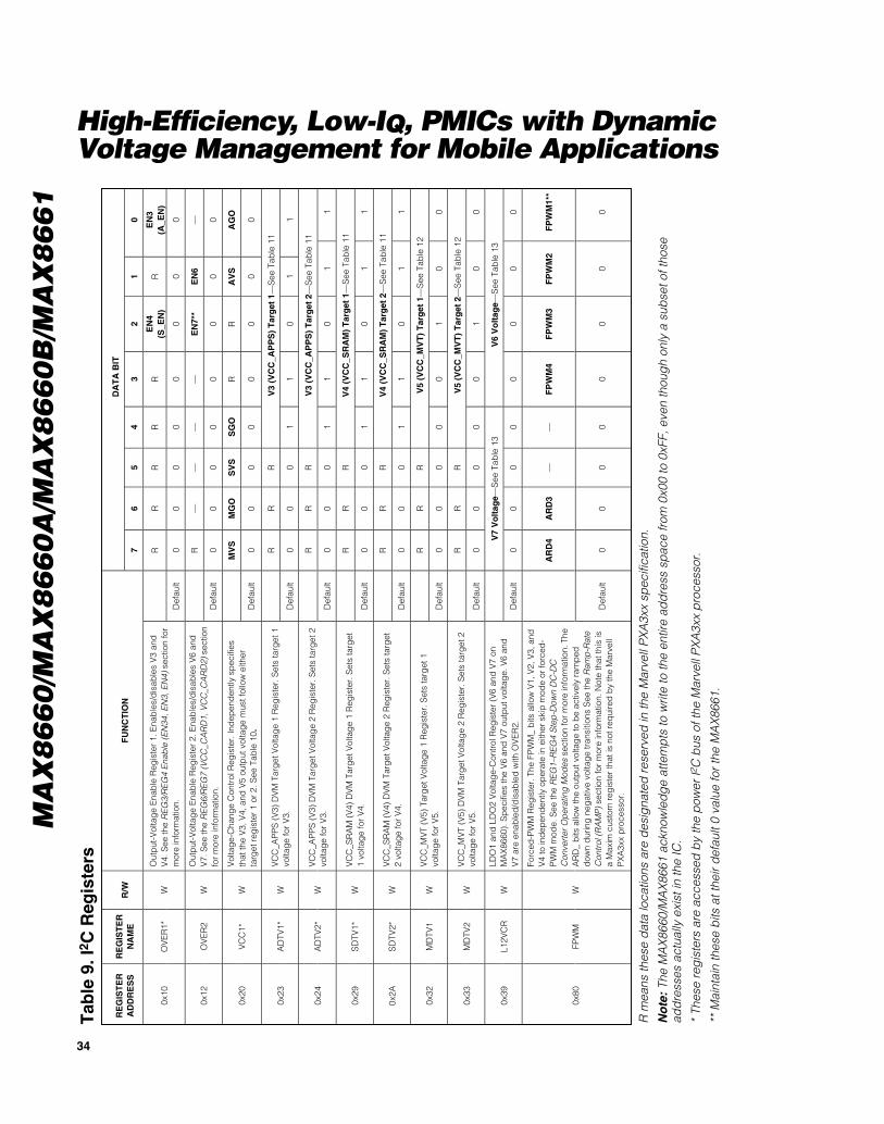
MA
X8
66
0/M
AX
86
60
A/M
AX
86
60
B/M
AX
86
61
High-Efficiency, Low-IQ, PMICs with DynamicVoltage Management for Mobile Applications
34
DA
TA
BIT
RE
GIS
TE
RA
DD
RE
SS
RE
GIS
TE
RN
AM
ER
/WF
UN
CT
ION
76
54
32
10
RR
RR
RE
N4
(S_E
N)
RE
N3
(A_E
N)
0x10
OV
ER
1*W
Out
put
-Vol
tag
e E
nab
le R
egis
ter
1. E
nab
les/
dis
able
s V
3 an
dV
4. S
ee th
e R
EG
3/R
EG
4 E
nab
le (
EN
34, E
N3,
EN
4) s
ectio
n fo
rm
ore
info
rmat
ion.
Def
ault
00
00
00
00
R—
——
—E
N7*
*E
N6
—0x
12O
VE
R2
WO
utp
ut-V
olta
ge
Ena
ble
Reg
iste
r 2.
Ena
ble
s/d
isab
les
V6
and
V7.
See
the
RE
G6/
RE
G7
(VC
C_C
AR
D1,
VC
C_C
AR
D2)
sec
tion
for
mor
e in
form
atio
n.D
efau
lt0
00
00
00
0
MV
SM
GO
SV
SS
GO
RR
AV
SA
GO
0x20
VC
C1*
WV
olta
ge-
Cha
nge
Con
trol
Reg
iste
r. In
dep
end
ently
sp
ecifi
esth
at th
e V
3, V
4, a
nd V
5 ou
tput
vol
tag
e m
ust f
ollo
w e
ither
targ
et r
egis
ter
1 or
2. S
ee T
able
10.
Def
ault
00
00
00
00
RR
RV
3 (V
CC
_AP
PS
) T
arg
et 1
—S
ee T
able
11
0x23
AD
TV1*
WV
CC
_AP
PS
(V
3) D
VM
Tar
get
Vol
tag
e 1
Reg
iste
r. S
ets
targ
et 1
volta
ge
for
V3.
Def
ault
00
01
10
11
RR
RV
3 (V
CC
_AP
PS
) T
arg
et 2
—S
ee T
able
11
0x24
AD
TV2*
WV
CC
_AP
PS
(V
3) D
VM
Tar
get
Vol
tag
e 2
Reg
iste
r. S
ets
targ
et 2
volta
ge
for
V3.
Def
ault
00
01
10
11
RR
RV
4 (V
CC
_SR
AM
) T
arg
et 1
—S
ee T
able
11
0x29
SD
TV1*
WV
CC
_SR
AM
(V
4) D
VM
Tar
get
Vol
tag
e 1
Reg
iste
r. S
ets
targ
et1
volta
ge
for
V4.
Def
ault
00
01
10
11
RR
RV
4 (V
CC
_SR
AM
) T
arg
et 2
—S
ee T
able
11
0x2A
SD
TV2*
WV
CC
_SR
AM
(V
4) D
VM
Tar
get
Vol
tag
e 2
Reg
iste
r. S
ets
targ
et2
volta
ge
for
V4.
Def
ault
00
01
10
11
RR
RV
5 (V
CC
_MV
T)
Tar
get
1—
See
Tab
le 1
20x
32M
DTV
1W
VC
C_M
VT
(V5)
Tar
get
Vol
tag
e 1
Reg
iste
r. S
ets
targ
et 1
volta
ge
for
V5.
Def
ault
00
00
01
00
RR
RV
5 (V
CC
_MV
T)
Tar
get
2—
See
Tab
le 1
20x
33M
DTV
2W
VC
C_M
VT
(V5)
DV
M T
arg
et V
olta
ge
2 R
egis
ter.
Set
s ta
rget
2vo
ltag
e fo
r V
5.D
efau
lt0
00
00
10
0
V7
Vo
ltag
e—S
ee T
able
13
V6
Vo
ltag
e—S
ee T
able
13
0x39
L12V
CR
WLD
O1
and
LD
O2
Vol
tag
e-C
ontr
ol R
egis
ter
(V6
and
V7
onM
AX
8660
). S
pec
ifies
the
V6
and
V7
outp
ut v
olta
ge.
V6
and
V7
are
enab
led
/dis
able
d w
ith O
VE
R2.
Def
ault
00
00
00
00
AR
D4
AR
D3
——
FP
WM
4F
PW
M3
FP
WM
2F
PW
M1*
*
0x80
FPW
MW
Forc
ed-P
WM
Reg
iste
r. T
he F
PW
M_
bits
allo
w V
1, V
2, V
3, a
ndV
4 to
ind
epen
den
tly o
per
ate
in e
ither
ski
p m
ode
or fo
rced
-P
WM
mod
e. S
ee th
e R
EG
1–R
EG
4 S
tep
-Dow
n D
C-D
CC
onve
rter
Op
erat
ing
Mod
es s
ectio
n fo
r m
ore
info
rmat
ion.
The
AR
D_
bits
allo
w th
e ou
tput
vol
tag
e to
be
activ
ely
ram
ped
dow
n d
urin
g n
egat
ive
volta
ge
tran
sitio
ns S
ee th
e R
amp
-Rat
eC
ontr
ol (
RA
MP
) se
ctio
n fo
r m
ore
info
rmat
ion.
Not
e th
at th
is is
a M
axim
cus
tom
reg
iste
r th
at is
not
req
uire
d b
y th
e M
arve
llP
XA
3xx
pro
cess
or.
Def
ault
00
00
00
00
Tab
le 9
. I2 C
Reg
iste
rs
R m
eans
thes
e d
ata
loca
tions
are
des
igna
ted
res
erve
d in
the
Mar
vell
PX
A3x
x sp
ecifi
catio
n.
No
te:
The
MA
X86
60/M
AX
8661
ack
now
led
ge
atte
mp
ts to
writ
e to
the
entir
e ad
dre
ss s
pac
e fr
om 0
x00
to 0
xFF,
eve
n th
oug
h on
ly a
sub
set o
f tho
sead
dre
sses
act
ually
exi
st in
the
IC.
* Th
ese
reg
iste
rs a
re a
cces
sed
by
the
pow
er I2
C b
us o
f the
Mar
vell
PX
A3x
x p
roce
ssor
.
** M
aint
ain
thes
e b
its a
t the
ir d
efau
lt 0
valu
e fo
r th
e M
AX
8661
.

MA
X8
66
0/M
AX
86
60
A/M
AX
86
60
B/M
AX
86
61
High-Efficiency, Low-IQ, PMICs with DynamicVoltage Management for Mobile Applications
35
START and STOP ConditionsWhen the serial interface is inactive, SDA and SCL idlehigh. A master device initiates communication by issuinga START condition. A START condition is a high-to-lowtransition on SDA with SCL high. A STOP condition is alow-to-high transition on SDA, while SCL is high (Figure 8).
A START condition from the master signals the begin-ning of a transmission to the MAX8660/MAX8661. Themaster terminates transmission by issuing a not-acknowledge followed by a STOP condition (see theAcknowledge Bit section for more information). TheSTOP condition frees the bus. To issue a series of com-mands to the slave, the master may issue repeatedstart (Sr) commands instead of a stop command inorder to maintain control of the bus. In general, arepeated start command is functionally equivalent to aregular start command.
When a STOP condition or incorrect address is detected,the MAX8660/MAX8661 internally disconnect SCL fromthe serial interface until the next START condition, mini-mizing digital noise and feedthrough.
Acknowledge BitBoth the master and the MAX8660/MAX8661 (slave)generate acknowledge bits when receiving data. Theacknowledge bit is the last bit of each 9-bit data packet.To generate an acknowledge (A), the receiving devicemust pull SDA low before the rising edge of the acknowl-edge-related clock pulse (ninth pulse) and keep it lowduring the high period of the clock pulse (Figure 9). Togenerate a not acknowledge (A), the receiving deviceallows SDA to be pulled high before the rising edge ofthe acknowledge-related clock pulse and leaves it highduring the high period of the clock pulse.
Monitoring the acknowledge bits allows for detection ofunsuccessful data transfers. An unsuccessful datatransfer occurs if a receiving device is busy or if a sys-tem fault has occurred. In the event of an unsuccessfuldata transfer, the bus master should reattempt commu-nication at a later time.
Slave AddressA bus master initiates communication with a slavedevice (MAX8660/MAX8661) by issuing a START condi-tion followed by the slave address. As shown in Figure10, the slave address byte consists of 7 address bitsand a read/write bit (R/W). After receiving the properaddress, the MAX8660/MAX8661 issue an acknowledgeby pulling SDA low during the ninth clock cycle. Notethat the R/W bit is always zero since the MAX8660/MAX8661 are write only.
The Marvell PXA3xx processor supports 0x68 (SRAD =GND) as the I2C slave address.
S PSr
SCL
SDA
tHD;STAtHD;STA
tSU;STOtSU;STA
Figure 8. START and STOP Conditions
tSU;DATtHD;DAT
S
SCL
SDA
1 2 8 9
NOT ACKNOWLEDGEACKNOWLEDGE
Figure 9. Acknowledge Bits
S
ACKNOWLEDGE
SCL
SDA
1 2 3
110
8 94 5 6 7
0 1 0 SRAD 0 A
SRAD
0 (GND)1 (IN)
SLAVE ADDRESS (WRITE)BINARY HEXADECIMAL
0x680x6A
0b 0110 10000b 0110 1010
R/W = 0(WRITE ONLY)
Figure 10. Slave Address Byte

MA
X8
66
0/M
AX
86
60
A/M
AX
86
60
B/M
AX
86
61
High-Efficiency, Low-IQ, PMICs with DynamicVoltage Management for Mobile Applications
36
I 2C Write OperationThe MAX8660/MAX8661 are write-only devices andrecognize the “write byte” protocol as defined in theSMBus specification and shown in section A of Figure11. The “write byte” protocol allows the I2C masterdevice to send 1 byte of data to the slave device. The“write byte” protocol requires a register pointer addressfor the subsequent write. The MAX8660/MAX8661acknowledge any register pointer even though only asubset of those registers actually exists in the device.The “write byte” protocol is as follows:
1) The master sends a start command.
2) The master sends the 7-bit slave address followedby a write bit.
3) The addressed slave asserts an acknowledge bypulling SDA low.
4) The master sends an 8-bit register pointer.
5) The slave acknowledges the register pointer.
6) The master sends a data byte.
7) The slave updates with the new data.
8) The slave acknowledges the data byte.
9) The master sends a STOP condition.
In addition to the write-byte protocol, the MAX8660/MAX8661 recognize the multiple byte register-data pairprotocol as shown in section B of Figure 11. This proto-col allows the I2C master device to address the slaveonly once and then send data to multiple registers in arandom order. Registers may be written continuouslyuntil the master issues a STOP condition.
The multiple-byte register-data pair protocol is asfollows:
1) The master sends a start command.
2) The master sends the 7-bit slave address followedby a write bit.
3) The addressed slave asserts an acknowledge bypulling SDA low.
4) The master sends an 8-bit register pointer.
5) The slave acknowledges the register pointer.
6) The master sends a data byte.
7) The slave updates with the new data.
8) The slave acknowledges the data byte.
9) Steps 5 to 7 are repeated as many times asthe master requires. Registers may be accessed inrandom order.
10)The master sends a STOP condition.
REGISTERADDRESS
REGISTERNAME
BIT NAME FUNCTION
7 MVSV5 (VCC_MVT) voltage select:0—Ramp V5 to voltage selected by MDTV1 (default)1—Ramp V5 to voltage selected by MDTV2
6 MGOStart V5 (VCC_MVT) voltage change:0—Hold V5 at current level (default)1—Ramp V5 as selected by MVS
5 SVSV4 (VCC_SRAM) voltage select:0—Ramp V4 to voltage selected by SDTV1 (default)1—Ramp V4 to voltage selected by SDTV2
4 SGOStart V4 (VCC_SRAM) voltage change:0—Hold V4 at current level (default)1—Ramp V4 as selected by SVS
3 R Reserved
2 R Reserved
1 AVSV3 (VCC_APPS) voltage select:0—Ramp V3 to voltage selected by ADTV1 (default)1—Ramp V3 to voltage selected by ADTV2
0x20 VCC1
0 AGOStart V3 (VCC_APPS) voltage change:0—Hold V3 at current level (default)1—Ramp V3 as selected by AVS
Table 10. DVM Voltage-Change Register (VCC1, 0x20)

MA
X8
66
0/M
AX
86
60
A/M
AX
86
60
B/M
AX
86
61
High-Efficiency, Low-IQ, PMICs with DynamicVoltage Management for Mobile Applications
37
Table 11. Serial Codes for V3 (VCC_APPS) and V4 (VCC_SRAM) Output Voltages
REGISTERADDRESS
REGISTERNAME
DATABYTE
OUTPUTVOLTAGE (V)*
0x00 0.7250x01 0.7500x02 0.7750x03 0.8000x04 0.8250x05 0.8500x06 0.8750x07 0.9000x08 0.9250x09 0.9500x0A 0.9750x0B 1.0000x0C 1.0250x0D 1.0500x0E 1.0750x0F 1.1000x10 1.1250x11 1.150**0x12 1.1750x13 1.2000x14 1.2250x15 1.2500x16 1.2750x17 1.3000x18 1.3250x19 1.3500x1A 1.3750x1B 1.400 (default)***0x1C 1.4250x1D 1.4500x1E 1.4750x1F 1.5000x20 1.5250x21 1.5500x22 1.5750x23 1.6000x24 1.6250x25 1.6500x26 1.6750x27 1.7000x28 1.7250x29 1.7500x2A 1.775
0x230x240x290x2A
ADTV1ADTV2SDTV1SDTV2
0x2B 1.800*Contact factory for other default voltages.**MAX8660B default voltage is 1.15V.***MAX8660/MAX8660A/MAX8661 default voltage is1.4V.
Table 12. Serial Codes for V5 OutputVoltage
Table 13. Serial Codes for V6 and V7Output Voltages
REGISTERADDRESS
REGISTERNAME
DATANIBBLE
OUTPUTVOLTAGE (V)
0x01.8
(default)
0x1 1.90x2 2.00x3 2.10x4 2.20x5 2.30x6 2.40x7 2.50x8 2.60x9 2.70xA 2.80xB 2.90xC 3.00xD 3.10xE 3.2
0x39 L12VCR
0xF 3.3
REGISTERADDRESS
REGISTERNAME
DATABYTE
OUTPUTVOLTAGE (V)
0x00 1.7000x01 1.7250x02 1.7500x03 1.775
0x041.800
(default)
0x05 1.8250x06 1.8500x07 1.8750x08 1.9000x09 1.9250x0A 1.9500x0B 1.975
0x320x33
MDTV1MDTV2
0x0C 2.000

MA
X8
66
0/M
AX
86
60
A/M
AX
86
60
B/M
AX
86
61
High-Efficiency, Low-IQ, PMICs with DynamicVoltage Management for Mobile Applications
38
1
S
NUMBER OF BITS
R/W
SLAVE ADDRESS
7
0
1 8
REGISTER POINTER
1 1 8
DATA A
1
P
1
SLAVE TO MASTER
MASTER TO SLAVE
LEGEND
1
S
R/W
SLAVE ADDRESS
7
0
1 8
REGISTER POINTER XA
1
AA
1 8
DATA X A
1
P
1
8
REGISTER POINTER n A
1 8
DATA n A
1
8
REGISTER POINTER Z A
1 8
DATA Z A
1
A. WRITING TO A SINGLE REGISTER WITH THE “WRITE BYTE” PROTOCOL
B. WRITING TO MULTIPLE REGISTERS WITH THE “MULTIPLE-BYTE REGISTER-DATA PAIR” PROTOCOL
NUMBER OF BITS
NUMBER OF BITS
NUMBER OF BITS
A A
Figure 11. Writing to the MAX8660/MAX8661
Design ProcedureSetting the Output Voltages
The REG1 and REG2 regulators each have three presetvoltages that are programmed with the SET1 and SET2inputs. See the REG1 (VCC_IO) Step-Down DC-DCConverter (MAX8660 Only) and REG2 (VCC_IO,VCC_MEM) Step-Down DC-DC Converters sections formore information. V8 is fixed at 3.3V and cannot bechanged.
V3–V7 are set by the I2C interface. See the I2CInterface section for more information. Note that whileoperating in forced-PWM mode with an input voltagegreater than 4.3V, the minimum output voltage of REG3and REG4 is limited by the minimum duty cycle. Inforced-PWM mode, the minimum output voltage forREG3 or REG4 is:
Note that the above minimum voltage limitation doesnot apply to normal-mode operation.
Inductor SelectionCalculate the inductor value (LIDEAL) for each of REG1through REG4 as follows:
This sets the peak-to-peak inductor current ripple to 1/4the maximum output current. The oscillator frequency,fOSC, is 2MHz, and the duty cycle, D, is:
Given LIDEAL, the peak-to-peak inductor ripple currentis 0.25 x IOUT(MAX). The peak inductor current is 1.125x IOUT(MAX). Make sure that the saturation current of theinductor exceeds the peak inductor current, and therated maximum DC inductor current exceeds the maxi-mum output current (IOUT(MAX)). Inductance valuessmaller than LIDEAL can be used to reduce inductorsize; however, if much smaller values are used, peakinductor current rises and a larger output capacitancemay be required to suppress output ripple. Larger
DVVOUT
IN=
Lx V x D x D
I x fIDEALIN
OUT MAX OSC=
−4 1( )
( )
V x V
V x VMIN PV
MIN PV
3 0 167
4 0 1673
4
==
.
.
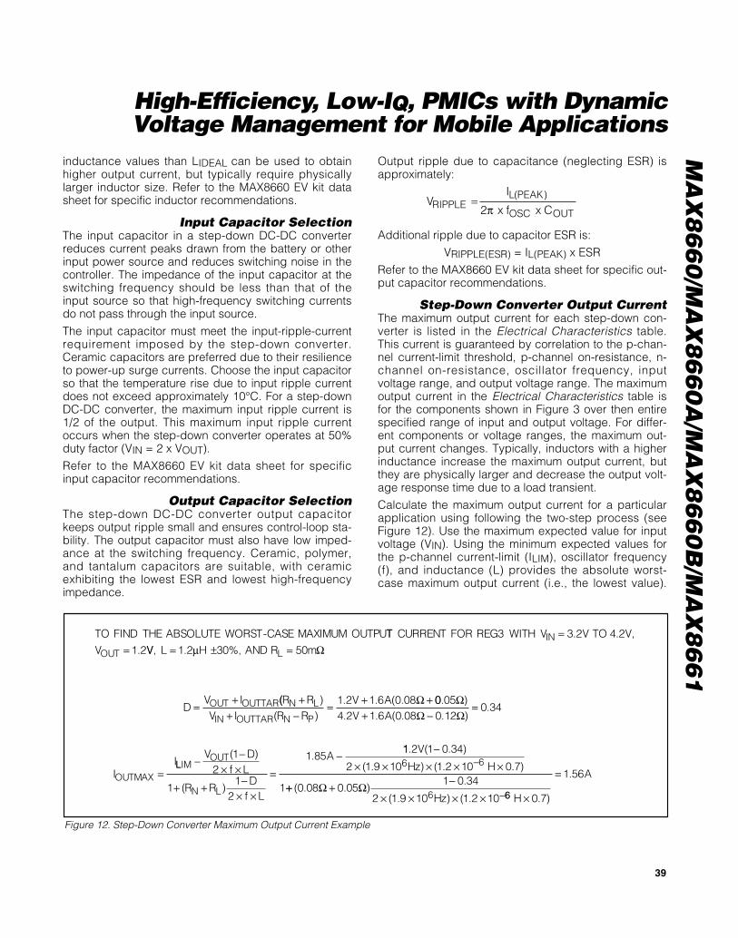
MA
X8
66
0/M
AX
86
60
A/M
AX
86
60
B/M
AX
86
61
High-Efficiency, Low-IQ, PMICs with DynamicVoltage Management for Mobile Applications
39
inductance values than LIDEAL can be used to obtainhigher output current, but typically require physicallylarger inductor size. Refer to the MAX8660 EV kit datasheet for specific inductor recommendations.
Input Capacitor SelectionThe input capacitor in a step-down DC-DC converterreduces current peaks drawn from the battery or otherinput power source and reduces switching noise in thecontroller. The impedance of the input capacitor at theswitching frequency should be less than that of theinput source so that high-frequency switching currentsdo not pass through the input source.
The input capacitor must meet the input-ripple-currentrequirement imposed by the step-down converter.Ceramic capacitors are preferred due to their resilienceto power-up surge currents. Choose the input capacitorso that the temperature rise due to input ripple currentdoes not exceed approximately 10°C. For a step-downDC-DC converter, the maximum input ripple current is1/2 of the output. This maximum input ripple currentoccurs when the step-down converter operates at 50%duty factor (VIN = 2 x VOUT).
Refer to the MAX8660 EV kit data sheet for specificinput capacitor recommendations.
Output Capacitor SelectionThe step-down DC-DC converter output capacitorkeeps output ripple small and ensures control-loop sta-bility. The output capacitor must also have low imped-ance at the switching frequency. Ceramic, polymer,and tantalum capacitors are suitable, with ceramicexhibiting the lowest ESR and lowest high-frequencyimpedance.
Output ripple due to capacitance (neglecting ESR) isapproximately:
Additional ripple due to capacitor ESR is:
VRIPPLE(ESR) = IL(PEAK) x ESR
Refer to the MAX8660 EV kit data sheet for specific out-put capacitor recommendations.
Step-Down Converter Output CurrentThe maximum output current for each step-down con-verter is listed in the Electrical Characteristics table.This current is guaranteed by correlation to the p-chan-nel current-limit threshold, p-channel on-resistance, n-channel on-resistance, oscillator frequency, inputvoltage range, and output voltage range. The maximumoutput current in the Electrical Characteristics table isfor the components shown in Figure 3 over then entirespecified range of input and output voltage. For differ-ent components or voltage ranges, the maximum out-put current changes. Typically, inductors with a higherinductance increase the maximum output current, butthey are physically larger and decrease the output volt-age response time due to a load transient.
Calculate the maximum output current for a particularapplication using following the two-step process (seeFigure 12). Use the maximum expected value for inputvoltage (VIN). Using the minimum expected values forthe p-channel current-limit (ILIM), oscillator frequency(f), and inductance (L) provides the absolute worst-case maximum output current (i.e., the lowest value).
VI
x f x CRIPPLEL PEAK
OSC OUT= ( )
2π
TO FIND THE ABSOLUTE WORST CASE MAXIMUM OUTPU- TT CURRENT FOR REG WITH V V TO V
VIN
OUT
3 3 2 4 2
1 2
==
. . ,
. VV L H AND R m
DV I
L
OUT OUTTAR
, . %,= ± =
=+
1 2 30 50µ Ω
(( )( )
. . ( .R RV I R R
V AN L
IN OUTTAR N P
++ −
=+ +1 2 1 6 0 08Ω 00 05
4 2 1 6 0 08 0 120 34
. ). . ( . . )
.Ω
Ω ΩV A
II
OUTMAX
+ −=
=LLIM
OUT
N L
V Df L
R RD
f L
A−−
× ×
+ + −× ×
=
−( )
( )
.12
11
2
1 8511 2 1 0 34
2 1 9 10 1 2 10 0 7
1
6 6. ( . )
( . ) ( . . )
V
Hz H
−× × × × ×−
++ + −× × × × −
( . . ).
( . ) ( .0 08 0 05
1 0 34
2 1 9 10 1 2 106Ω Ω
Hz 66 0 7
1 56
H
A
×
=
. )
.
Figure 12. Step-Down Converter Maximum Output Current Example

MA
X8
66
0/M
AX
86
60
A/M
AX
86
60
B/M
AX
86
61 Conservative designers can choose to use the mini-
mums for ILIM, f, and L, however, it is statistically rarefor all three of these parameters to be at the minimumvalue in any one given design. A more practicalmethod is to look at the how each individual variabledegrades the maximum output current and then takethe RMS of each variables contribution. Refer to thespreadsheet (www.maxim-ic.com/tools/other/soft-ware/MAX8660-step-down_output_current.xls) foreasy evaluation of the maximum output current. It pro-vides results for both the absolute worst case and RMScalculation methods.
1) Use the following equation to calculate the approxi-mate duty cycle (D):
where:
VOUT = output voltage
IOUTTAR = target (desired) output current—cannotbe more than the minimum p-channel current-limitthreshold
RN = n-channel on-resistance
RP = p-channel on-resistance
RL = external inductor’s ESR
VIN = input voltage—MAXIMUM
2) Use the following equation to calculate the maximumoutput current (IOUTMAX):
where:ILIM = p-channel current-limit threshold—MINIMUM
VOUT = output voltage
D = approximate duty cycle derived from step 1
f = oscillator frequency—MINIMUM
L = external inductor’s inductance—MINIMUM
RN = n-channel on-resistance
RL = external inductor’s ESR
Applications InformationPower Dissipation
The MAX8660/MAX8661 have a thermal-shutdown fea-ture that protects the IC from damage when the die tem-perature exceeds +160°C (see the Thermal-OverloadProtection section for more information). To prevent ther-mal overload and allow the maximum load current oneach regulator, it is important to ensure that the heatgenerated by the MAX8660/MAX8661 can be dissipatedinto the PC board. The exposed pad must be soldered tothe PC board, with multiple vias under the exposed pad(EP) conducting heat to a ground plane.
The junction-to-case thermal resistance (θJC) of theMAX8660/MAX8661 is 2.7°C/W. When properly mount-ed on a multilayer PC board, the junction-to-ambientthermal resistance (θJA) is typically 28°C/W.
PCB Layout and RoutingGood printed circuit board (PCB) layout is necessary toachieve optimal performance. Conductors carrying dis-continuous currents and any high-current path must bemade as short and wide as possible.
Refer to the MAX8660 EV kit data sheet for an exampleof a good PCB layout. Place the bypass capacitors foreach power input pair (IN to AGND, PV1 to PG1, PV2 toPG2, PV3, to PG3, and PV4 to PG4) as close as possibleto the IC.
The exposed pad (EP) is the main path for heat to exitthe IC. Connect EP to the ground plane with multiplevias to allow heat to dissipate from the device.
II
V Df L
R RD
f
OUTMAXLIM
OUT
N L
=−
−× ×
+ + −× ×
( )
( )
12
11
2 LL
DV I R RV I R ROUT OUTTAR N L
IN OUTTAR N P=
+ ++ −
( )( )
High-Efficiency, Low-IQ, PMICs with DynamicVoltage Management for Mobile Applications
40

MA
X8
66
0/M
AX
86
60
A/M
AX
86
60
B/M
AX
86
61
High-Efficiency, Low-IQ, PMICs with DynamicVoltage Management for Mobile Applications
41
“yww” is a date code.“aaaa” is an assembly code.
8660ETLyww+ aaaa
8660AETLyww+ aaaa
8661ETLyww+ aaaa
TOP VIEW
Package Marking
+Denotes lead-free packaging and marks pin 1 location.
Chip InformationPROCESS: BiCMOS
Ordering Information (continued)PART PIN-PACKAGE OPTIONS
M AX 8660AE TL+ 40 Thin QFN
V 1: 2.5V , 2.0V , 1.8V V 2: 2.5V , 2.0V , 1.8V V 3: 1.4V ( d efaul t) V 4: 1.4V ( d efaul t)
M AX 8660BE TL+ 40 Thin QFN
V 1: 3.3V , 3.0V , 2.85V V 2: 3.3V , 2.5V , 1.8V V 3: 1.15V ( defaul t) V 4: 1.15V ( defaul t)
MAX8661ETL+ 40 Thin QFN
N o RE G1 and RE G7V 2: 3.3V , 2.5V , 1.8V V 3: 1.4V ( d efaul t) V 4: 1.4V ( d efaul t)
Note: All devices are specified over the -40°C to 85°C operatingtemperature range.+Denotes lead(Pb)-free/RoHS-compliant package.

MA
X8
66
0/M
AX
86
60
A/M
AX
86
60
B/M
AX
86
61
High-Efficiency, Low-IQ, PMICs with DynamicVoltage Management for Mobile Applications
42
PACKAGE TYPE PACKAGE CODE DOCUMENT NO.
40 TQFN T4055-1 21-0140
Package InformationFor the latest package outline information and land patterns, go to www.maxim-ic.com/packages. Note that a “+”, “#”, or “-” in thepackage code indicates RoHS status only. Package drawings may show a different suffix character, but the drawing pertains to thepackage regardless of RoHS status.
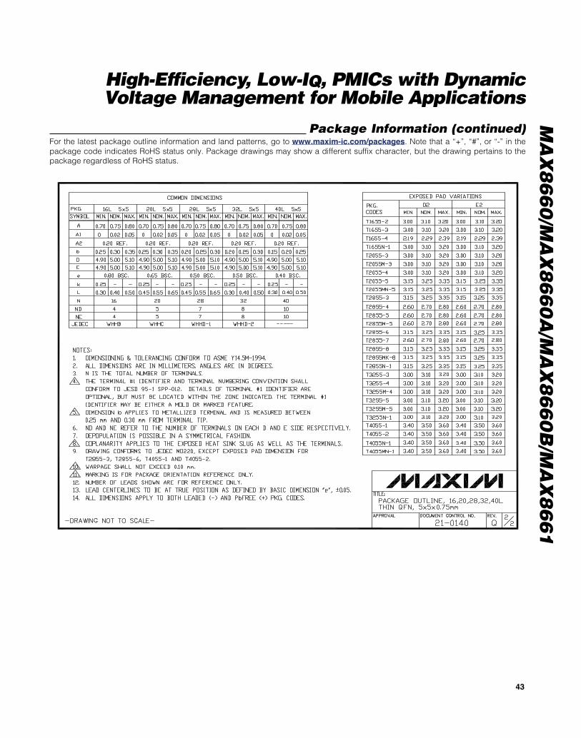
MA
X8
66
0/M
AX
86
60
A/M
AX
86
60
B/M
AX
86
61
High-Efficiency, Low-IQ, PMICs with DynamicVoltage Management for Mobile Applications
43
Package Information (continued)For the latest package outline information and land patterns, go to www.maxim-ic.com/packages. Note that a “+”, “#”, or “-” in thepackage code indicates RoHS status only. Package drawings may show a different suffix character, but the drawing pertains to thepackage regardless of RoHS status.

MA
X8
66
0/M
AX
86
60
A/M
AX
86
60
B/M
AX
86
61
High-Efficiency, Low-IQ, PMICs with DynamicVoltage Management for Mobile Applications
Maxim cannot assume responsibility for use of any circuitry other than circuitry entirely embodied in a Maxim product. No circuit patent licenses areimplied. Maxim reserves the right to change the circuitry and specifications without notice at any time. The parametric values (min and max limits) shown inthe Electrical Characteristics table are guaranteed. Other parametric values quoted in this data sheet are provided for guidance.
44 _______________Maxim Integrated Products, Inc. 160 Rio Robles, San Jose, CA 95134 USA 1-408-601-1000
© 2012 Maxim Integrated Products Maxim is a registered trademark of Maxim Integrated Products, Inc.
Revision History
REVISIONNUMBER
REVISIONDATE
DESCRIPTIONPAGES
CHANGED
2 8/09Added MAX8660B and automotive part options, and replaced Intel references withMarvell
1, 2, 3, 5, 6, 7,10, 11, 19–34,
36, 37
3 6/10
Added reference to Marvell’s Armada 100 family of processors, added solderingtemperature, corrected an error with REG4’s p-Channel Current Limit Threshold,added Step-Down Converter Output Current section, improved data sheetconsistency and style
1, 2, 5, 6, 7, 10,11, 12, 14, 15,25, 26, 30, 33,
35, 39