high-efficiency dye-sensitized solar cell with three...
TRANSCRIPT
Published: September 30, 2011
r 2011 American Chemical Society 4579 dx.doi.org/10.1021/nl201792r |Nano Lett. 2011, 11, 4579–4584
LETTER
pubs.acs.org/NanoLett
High-Efficiency Dye-Sensitized Solar Cell with Three-DimensionalPhotoanodeNicolas T�etreault,*,† �Eric Arsenault,‡ Leo-Philipp Heiniger,† Navid Soheilnia,‡ J�er�emie Brillet,†
Thomas Moehl,† Shaik Zakeeruddin,† Geoffrey A. Ozin,*,‡ and Michael Gr€atzel†
†Laboratory of Photonic and Interfaces, Institute of Physical Chemistry, �Ecole Polytechnique F�ed�erale de Lausanne, 1015 Lausanne,Switzerland‡Materials Chemistry and Nanochemistry Research Group, Center for Inorganic and Polymeric Nanomaterials, Department ofChemistry, University of Toronto, 80 St. George Street, Toronto, Ontario M5S 3H6, Canada
bS Supporting Information
Dye-sensitized solar cells (DSCs) are one of the most pro-mising photovoltaic technologies for production of renewable,
clean, and affordable energy. They are generally made from cheapand nontoxic components and can be designed in a variety ofdifferent colors and transparencies, which distinguishes them asan ideal photovoltaic concept for integrated “green” architecture.Additionally, they have been shown to be competitive with otherthin film technologies reaching certified efficiencies as high as11.1% when using a triiodide/iodide (I3
�/I�) redox shuttle.1�3
In DSCs, charge carrier generation takes place in a chemi-sorbedmonolayer of photoactive dye that is sandwiched betweena semiconducting oxide, usually anatase TiO2, and an electrolyteacting as electron and hole conducting materials, respectively.Because of the relatively low-absorption cross-section of themolecular sensitizer, a high surface area mesoscopic photoanodeis necessary to ensure high dye loading and efficient lightharvesting in the visible part of the solar spectrum. This impliesthat the DSC has an exceedingly large, heterogeneous interfacethrough which electrons may be (parasitically) intercepted as aresult of the slow electron transport. The latter is governed by anambipolar diffusion mechanism controlled by trap-limited hop-ping through a relatively long and tortuous path to the transpar-ent conductive electrode.4�7 It is further hindered by the lowelectron mobility in anatase TiO2 nanoparticles and the multiplegrain boundaries in the mesoporous film.8
Given a charge collection time ofmilliseconds at themaximumpower point,9 efficient charge extraction is only made possiblewhen using the (I3
�/I�) redox couple through the slow interception
of electrons by adjacent I3�.10 In addition to limited light harvesting
by the dye, one of the main limiting factors of efficiency is theexcessive driving force of 0.6 eV necessary for the dye-regenerationprocess leading to a significant loss-in-voltage of approximately 600mV.7,11,12 This has sparked development and study of variousalternative redox couples including p-type semiconductors.13 In-creasingly, development has been centered around the use oforganic hole-transporting materials (HTM) in solid-state DSCs(ss-DSCs).14�17
The electronic loss that is typically discussed for DSCs is slowtransport-induced recombination.18�21 If charges recombinebefore reaching the electrode then this has a direct influenceon the photocurrent and photovoltage. The open-circuit voltageis defined by the splitting of the quasi-Fermi level of electrons inthe metal oxide and the redox potential of the electrolyte (quasi-Fermi level of holes in the hole-transporter). Hence, the closerthe Fermi level in the metal oxide can be pushed toward theconduction band and LUMO level of the sensitizer, the higherthe open-circuit voltage, and the smaller the loss-in-potentialgoing from the level of the excited state of the dye to the quasi-Fermi level in the metal oxide. Two strategies can contribute tothis upward shift and increase the open-circuit potential, namelyreducing the recombination rate constant enabling the Fermi levelto move closer to the conduction band before the recombination
Received: May 26, 2011Revised: September 25, 2011
ABSTRACT:Herein, we present a straightforward bottom-up synthesis of a high electronmobility and highlylight scattering macroporous photoanode for dye-sensitized solar cells. The dense three-dimensional Al/ZnO,SnO2, or TiO2 host integrates a conformal passivation thin film to reduce recombination and a large surface-area mesoporous anatase guest for high dye loading. This novel photoanode is designed to improve thecharge extraction resulting in higher fill factor and photovoltage for DSCs. An increase in photovoltage of upto 110 mV over state-of-the-art DSC is demonstrated.
KEYWORDS: Phovoltaic devices, dye-sensitized solar cells, host�guest, self-assembly, transparent con-ductive oxides
4580 dx.doi.org/10.1021/nl201792r |Nano Lett. 2011, 11, 4579–4584
Nano Letters LETTER
rate balances the charge generation rate or shifting the conduc-tion band itself. Finally, enhancing the electron transport couldimprove charge collection and reduce IR losses, enhance theshort-circuit current, and fill factor.12,18
Several approaches have been proposed in order to reduceinterfacial recombination and improve charge collection in liquidelectrolytes and ss-DSCs including the use of radial collectionnanostructures,7 one-dimensional ZnO and TiO2 nanorods, andnanowires as photoanodes.22�25 Even though these approachesshow great promise, they have yet to achieve power conversionefficiencies above 5% in liquid electrolyte DSCs and 1.7% in ss-DSCs. Lately, we were able to show faster electron transportusing a novel three-dimensional (3D) self-assembled anataseTiO2 fibrous network photoanode capable of enhanced lightharvesting and charge transport to reach an efficiency of 5%, arecord for nanowire-based ss-DSCs.26
Particular attention has been given to ZnO and SnO2 asalternatives to TiO2 in DSCs due to their higher electronicconductivity and electron mobility when compared to TiO2.
27
Despite faster electron transport,27 only rather poor deviceefficiencies have been reported to date for DSCs employingnanocrystalline SnO2.
7,23,28�30 In part, this was found to be dueto a 2�3 orders of magnitude increase in the recombination rateswhen the high mobility material is in direct contact with thesensitizer and/or the electrolyte.27 This finding led to a host ofpublications on the addition of blocking (passivating) layerscovering the ZnO or SnO2 in order to reduce this recombinationrate resulting in higher photovoltage.7,31,32
Herein, we demonstrate a novel bottom-up 3D host�passi-vation�guest (H-P-G) electrode concept that enables structuralcontrol on the electron extraction, conduction band, and therecombination dynamics as well as on the optical scattering inphotovoltaic devices. This new type of electrode is exemplifiedherein by incorporating it into a DSC photoanode to significantlyimprove photocurrent, fill factor, and most importantly the
photovoltage. This is shown through a strong decrease in darkcurrent when comparing a 3D TiO2 host to high electronmobility Al/ZnO and SnO2 hosts. To ensure high dye loading,the macropores contained in the passivated 3D host are infil-trated with anatase TiO2 nanoparticles to form a conformalmesoporous film enabling optimized sensitization and electroninjection characteristics found in traditional nanoparticle-basedDSCs. Using this novel architecture, an increase in the photo-voltage of up to 110 mV over state-of-the-art TiO2, ZnO, andSnO2-based DSCs is obtained. The straightforward and simplebottom-up fabrication technique produces a highly opticallyscattering photoanode that could enable enhanced lightharvesting,1 fast charge extraction, reduced interfacial recombi-nation, and lower IR loss to significantly increase the cellphotovoltage, photocurrent, and the fill factor.12 The conceptelectrode is well suited for DSCs since only a small volumefraction is lost to the optically inactive 3D host material leavingmost of the volume for the light harvesting sensitized nanopar-ticle TiO2 mesoporous film.
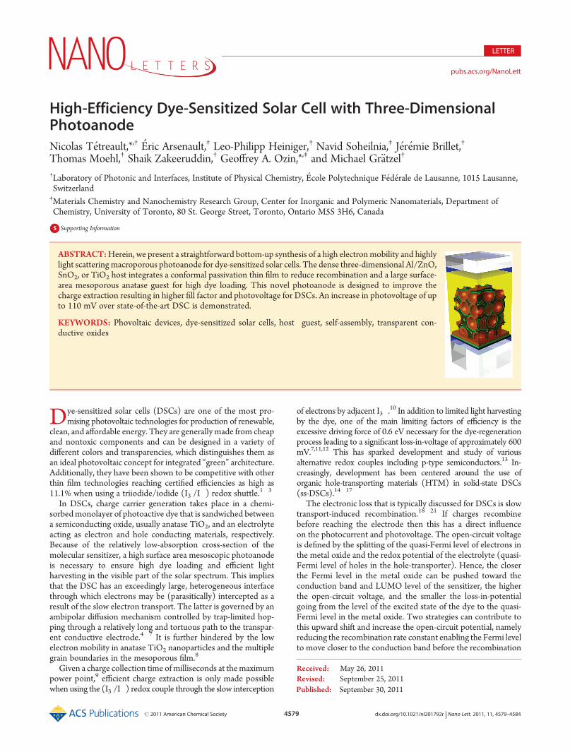
A schematic representation of the intermediate materialsinvolved in the fabrication of a 3D H-P-G photoanode for DSCsis shown in Figure 1. The overall fabrication method is inspiredby micromolding in inverse opals (MISO) first developed for thesynthesis of large-area oxide inverse opals and then extended forhigh-temperature fabrication of full-photonic bandgap semicon-ductor photonic crystals from polymer templates.33,34 In parti-cular, a dispersion of polystyrene macrospheres in isopropanol isused to accelerate the capillary force-induced self-assembly of thepolystyrene macrospheres (Φ = 2.2 μm) and thereby obtain ahighly disordered opal template of uniform thickness. Using largemonodispersed spheres enables the formation of a uniform tem-plate with predictably large interconnecting pores extending in allthree spatial dimensions. The thickness of the template is adjustedthrough the volume concentration of spheres in the isopro-panol dispersion (∼22 vol % for 10�12 μm thick template film).
Figure 1. Schematic representation of the synthesis method for a 3D host�guest dye-sensitized solar cell. (A) Doctor-bladed, disordered template of2.2 μm polystyrene spheres. (B) Layer-by-layer conformal deposition of the host material (Al/ZnO, TiO2) by ALD. (C) After RIE to open the topsurface, the template is removed by annealing at 360 �C to reveal a disordered inverse opal of host material. It is then conformally coated with 25 nm ofdense TiO2 by ALD. (D) Pore filling with high surface area nanocrystalline TiO2 and dye loading. (E) Liquid electrolyte infiltration and sealing of the dyesensitized solar cell.
4581 dx.doi.org/10.1021/nl201792r |Nano Lett. 2011, 11, 4579–4584
Nano Letters LETTER
The dispersion is then doctor bladed, a scalable fabricationtechnique, on a transparent conductive FTO-covered glasssubstrate to reveal a large-area highly light scattering disorderedtemplate (Figure 1a). It is then heated and infiltrated with 90 nmof Al/ZnO (1:9), SnO2, or TiO2 in a highly conformal fashion byatomic layer deposition (ALD) by alternating pulses of organo-metallic precursors and hydrolytic polycondensation agent(H2O) in exposure mode (Figure 1b). Recently ALD has beengaining interest as a powerful research tool for creating highlyconformal layers on nanostructured electrodes35 and has evenbeen used for surface state passivation of TiO2 in dye sensitizedsolar cells and Fe2O3 in photolysis.
36,37 The deposition tempera-ture is optimized to increase the template interconnecting poresize by softening of the polymer beads ensuring proper spherenecking.38 Large interconnecting pores between spheres willenable proper filling with the guest nanocrystalline TiO2 later on.A quick dry reactive ion etching (RIE) of the infiltrated opal’s topsurface oxide is performed before removing the polymer tem-plate by annealing (360 �C, 15 min.) We thus obtain a 3D hostbackbone that is well connected to the underlying FTO�glassfront electrode. The direct electronic connection will ensureefficient charge extraction throughout the interconnected 3DH-P-G electrode. The surfaces of the TCO backbone are thenconformally coated with 25 nmof dense TiO2 by ALD in order toreduce interfacial recombination between electrons in the highlyconducting TCO backbone and the I3
� oxidized electrolyte(Figure 1c).27 After calcination (500 �C, 15 min.) the hexagonalwurtzite, cassiterite, and anatase crystal structures of the Al/ZnO,SnO2, and TiO2, respectively, were confirmed by powder X-raydiffraction (see Supporting Information, Figure S1). In order toprovide enough surface area for dye sensitization and efficientlight harvesting, the macroporous inverse TCO backbone isinfiltrated by sequential doctor-blading of a low viscosity 17 nmanatase nanocrystal paste (Figure 1d).
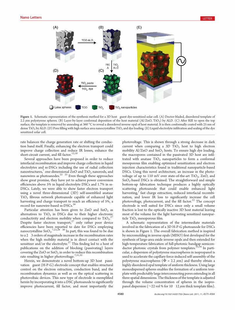
Scanning electron micrographs (SEM) of a 3D Al/ZnO|TiO2| anatase nanoparticles H-P-G photoanode are presentedin Figure 2. The cross-sectional and top view (Al/ZnO host)micrographs (Figure 2a,b) clearly show the high pore connectiv-ity throughout the 3D open structure as well as the significant
disorder inherited from the polystyrene template. From thesemicrographs, we can conclude that the backbone only uses asmall volume fraction of the 3D film (∼10%). This is anadditional advantage of the 3D macroporous structure wherethe high degree of necking between the templating spheres andthe very thin (90 nm) film of metal oxide host deposited leave thevast majority of the volume for filling with the guest material. Themacroporous structure further enables the conformal coating ofthe 3D host on both sides with dense TiO2 by ALD (Figure 2c,d).The role of the TiO2 overlayer is to passivate the TCO surface toimprove its chemical stability and further reduce recombinationrate at the conductive transparent oxide - electrolyte interface.Visible in Figure 2c is the direct contact between the 3D host andthe FTO�glass that will ensure unhindered electron transferfrom the 3D host�guest structure and the front DSC electrode.Additionally, subsequent TiO2 deposition was found to cover theFTO in addition to the 3D host to effectively block recombina-tion at the FTO�electrolyte interface. Figure 2e shows the 3DAl/ZnO |TiO2| anatase nanoparticles H-P-G electrode afterpartial filling with mesoporous anatase to constitute the fin-ished 3D TCO photoanode. We estimate from SEM picturesthat about 50% on the internal volume is filled with the anataseTiO2 nanoparticles. The disordered structure and the partialfilling at the scale of light combine to induce high opticalscattering in the 3D H-P-G structure (see Supporting Informa-tion, Figure S2)
Complete DSC devices were prepared using 10�12 μm thick3D TiO2 |TiO2| anatase nanoparticles, Al/ZnO |TiO2| anatasenanoparticles and SnO2 |TiO2| anatase nanoparticles H-P-Gphotoanodes on a FTO�glass substrate. In both cases, 90 nm ofthe host and 25 nm of TiO2 were deposited by ALD for amaximumwall thickness of 140 nm. Each of the macroporous 3DH-P-G structures were partially filled with a 17 nm anatasenanoparticle paste using a modified doctor blading procedure.Individual infiltrations were separated by 10 min heating at120 �C to ensure solvent evaporation and densification of theconformal paste thin film. The electrode is then calcined to burnoff the organic materials found in the paste (500 �C, 60 min,2 �C/min ramp).39 In order to improve the anatase nanoparticle
Figure 2. Scanning electron micrograph of a self-assembled 3D Al/ZnO |TiO2| host�guest dyes-sensitized solar cell photoanode. (A) Cross-sectionalview of a disordered TiO2 passivated 3D Al/ZnO backbone. (B) Top-view of the 3D macroporous Al/ZnO after top surface removal by reactive ionetching and template removal by annealing. (C) High-magnification micrograph showing the TiO2 covered 3D macroporous Al/ZnO host in directcontact with the front FTO electrode. (D) High-magnification micrograph showing the 3D Al/ZnO conformally coated with a 25 nm thin film of denseTiO2 inside and out. (E) Complete photoanode after infiltration and calcination of the TiO2 nanoparticle paste.
4582 dx.doi.org/10.1021/nl201792r |Nano Lett. 2011, 11, 4579–4584
Nano Letters LETTER
connectivity and increase the photocurrent, the TiO2 and SnO2
H-P-G photoanodes were immersed into a 40 mM aqueousTiCl4 solution at 70 �C for 30 min and washed with water andethanol.39 This treatment could not be done on the Al/ZnO-based electrode since it is not chemically stable enough to sustainimmersion in strong acid at elevated temperature. We shouldthus expect a penalty on the photocurrent for this photoanode.
The films are sintered for 30 min at 500 �C before dipping in a0.3 mM Z907 solution for 10 min. Z907 has been supplantedrecently by ruthenium and organic dyes with higher molarcoefficient but we were willing to sacrifice some photocurrentin exchange for high versatility and well-characterized photo-voltaic characteristics enabling a direct comparison with pub-lished data (Z907: Jsc = 17.13 mA/cm2, Voc = 730 mV, ff = 0.724,η = 9.05%).40 Following the immersion procedure, the dye-sensitized electrodes were rinsed with acetonitrile and dried inair. The photoanodes are then assembled using a thermallyplatinized FTO (TEC15) counter electrode using a 25 μm thickhot melt ring and sealed by heating. The cell internal space wasfilled with a I3
�/I� electrolyte in a 85:15 acetonitrile/valeronitrilemixture.
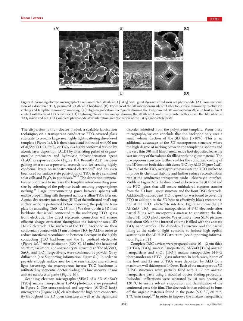
Shown in Figure 3a are the J�V characteristics for the dye-sensitized solar cells based on TiO2, SnO2, and Al/ZnO 3D hostphotoanodes. We find an increase in short-circuit current densitygoing from a TiO2 (Jsc = 6.9 mA/cm2) to Al/ZnO (Jsc = 7.9 mA/cm2) and SnO2 (Jsc = 10.4 mA/cm2). The photocurrent for theAl/ZnO host is found to be significantly lower than that of SnO2
because of the lack of TiCl4 treatment on the former. Thistreatment enhances connectivity between anatase TiO2 nano-particles to significantly increase the photocurrent and photo-voltage in state-of-the-art DSCs by improving electron hoppingat the anatase nanoparticle boundaries.41 Even though the Al/ZnO host is protected by TiO2 it is impossible to ensure acomplete, pinhole free protection against the low pH TiCl4
solution. It is possible that the increase in photocurrent observedis a direct consequence of the high electron mobility in the Al/ZnO and SnO2 hosts (241 and 16.5 cm2/(V s), respectively),which is 5�6 orders of magnitude higher than measured foranatase TiO2 nanoparticles at high voltage (V = 0.8 V, 2.30 �10�4 cm2/(V s)) (see Supporting Information, Table S1).8 Inaddition, the fill factor is found to be greater for the Al/ZnO (ff =0.77) host than for the TiO2 (ff = 0.73) host. Regardless of thehost material, the 3D H-P-G photoanodes all present photo-voltages well above the Voc = 730 mV obtained with the bestperforming Z907 DSCs.40 Indeed, an improvement of 60 and110 mV for TiO2 (Voc = 791 mV) and Al/ZnO (Voc = 842 mV)hosts are obtained, respectively. A significant increase in photo-voltage is to be expected when reducing the dark current whichdepends on the conduction band position and recombinationdynamics in the cell. Indeed, a significant decrease in the darkcurrent is observed going from the TiO2 to the Al/ZnO host ascan be seen in 3b. Further variations in the J�V characteristics fortwo additional dye/coadsorbent configurations (Z907/GBA andN719) are presented in the Supporting Information Figure S3.
When compared to previous studies using high mobilitymaterials like SnO2 and ZnO passivated with TiO2 in liquidelectrolyte DSCs we find that the photovoltage obtained with the3D host�guest photoanodes are higher by at least 90�100mV.7,23,28�30 Additionally, an increase of about 60 and 110 mVover our published state-of-the-art values for Z907 dye andiodine-based volatile electrolyte is obtained for 3D TiO2 andAl/ZnO hosts, respectively. One of the major advantages in usingtransparent high mobility materials, for example, ZnO and SnO2,for charge injection and collection in DSCs lies in its relativelylow transport resistance when compared to that of anatase TiO2
nanoparticles.42�44 However, this advantage was found to becounterbalanced by faster electron recombination dynamics withthe oxidized electrolyte via intrabandgap surface states ultimatelylimiting the efficiency of such cells.44 This led to the study of vari-ous capping materials (Al2O3, TiO2, MgO, etc.) that slowdown recombination leading to increases in photocurrent andphotovoltage.7,31,32 In addition to acting as an effective protec-tion layer for the chemically unstable ZnO against the acidic dyesolution,45 the complete coverage of the host material with ALDof a dense 25 nm TiO2 layer can passivate surface traps37 andincrease charge transfer resistance to the oxidized dye andelectrolyte. This is clearly visible in the decrease in dark currentobserved (Figure 3b). According to the literature, this can be dueto a decrease in recombination or a shift of the conduction bandtoward vacuum. Both would lead to a shift in the quasi-Fermilevel with respect to the redox potential of the electrolyte andcontribute to the significant increase in the observedphotovoltage.7 These findings will motivate further mechanisticstudies on the role of the various interfaces, conduction path-ways, and electronic properties of the various materials that couldinduce band bending, affect injection dynamics, or shift theconduction band position.
In conclusion, we demonstrated a novel bottom-up 3DH-P-GDSC photoanode made of a high electron mobility host, apassivating conformal blocking layer and a high surface areaguest to improve short circuit current density, fill factor, andphotovoltage. The 3D H-P-G photoanode shows a strongdecrease in dark current when using Al/ZnO with electronmobility and diffusion coefficient up to 6 orders of magnitudehigher than that of anatase TiO2 nanoparticles. By completelycovering the 3D host with a dense passivating TiO2 thin film and
Figure 3. Photocurrent density�voltage (J�V) characteristics of the3D host-passivation-guest dye-sensitized solar cells under AM 1.5illumination and in the dark. Solid (A) and dashed (B) lines representthe current under standard illumination and in the dark, respectively, forAl/ZnO (red, Jsc = 7.5 mA/cm2, Voc = 842 mV, ff = 0.77, η = 4.9%),SnO2 (blue, Jsc = 10.4 mA/cm2, Voc = 803 mV, ff = 0.70, η = 5.8%) andTiO2 (black, Jsc = 6.9 mA/cm
2, Voc = 791 mV, ff = 0.73, η = 4.0%) hosts.
4583 dx.doi.org/10.1021/nl201792r |Nano Lett. 2011, 11, 4579–4584
Nano Letters LETTER
filling its macropores with anatase nanoparticles, we ensure ahigh surface area for dye loading andmaintain injection dynamicstypical of anatase nanoparticle-based DSCs. Using this novel 3DH-P-G morphology partially filled with anatase nanoparticles, weshow an increase in photovoltage of up to 110 mV over state-of-the-art TiO2 and ZnO DSCs with Z907 and I3
�/I� redox couple.The concept electrode is well suited for DSC since only a smallvolume fraction is lost to the transparent 3D host material leavingmost of the volume for the light harvesting sensitized mesopor-ous anatase TiO2. The straightforward and simple bottom-upfabrication technique produces a highly optically scattering 3Dphotoanode material that could enhance light harvesting andcharge extraction and reduce interfacial recombination to sig-nificantly increase the cell photovoltage, photocurrent and the fillfactor in various low cost photovoltaic technologies.46
Methods. Three-Dimensional Host�Passivation�GuestPhotoanode Fabrication. A 22 vol % dispersion of 2.2 μmpolystyrene macrospheres in isopropanol is doctor bladed ona TEC15 FTO-covered glass substrate to reveal a large-areahighly light scattering disordered template. It is then heatedand infiltrated with 90 nm of Al/ZnO (1:9), SnO2, or TiO2 ina highly conformal fashion by atomic layer deposition (ALD)pulses of trimethylaluminum, diethylzinc and water (Al(Me)3,Zn(Et)2|H2O, 114 �C, 1:9), tetrakis(dimethylamino)tin andozone (Sn(NMe2)4|O3, 200 �C) and tetrakis(dimethylamino)-titanium and water (Ti(NMe2)4|H2O, 200 �C) using nitrogenas a carrier gas (Cambridge Nanotech Savannah S100). Theinfiltrated opal’s top surface oxide is removed by RIE (6 min,1800W, C4F8, Ar carrier gas, AMS200) performed beforeremoving the polymer template by annealing (360 �C, 15 min.)The TCO backbone is then conformally coated with 25 nm ofdense TiO2 by ALD in order to reduce interfacial recombinationbetween electrons in the highly conducting TCO backboneand the I3
� oxidized electrolyte (Figure 1c).27 The 3D H-P-Gstructures were filled with a 17 nm anatase nanoparticle pastethrough four sequential doctor blading separated by 10 minheating at 120 �C to ensure solvent evaporation and densi-fication of the conformal paste thin film. The electrode is thencalcined to burn off the organic materials found in the paste(500 �C, 60 min, 2 �C/min ramp).39 In order to improve theanatase nanoparticle connectivity and increase the photocur-rent, the TiO2 and SnO2 H-P-G photoanodes were immersedinto a 40 mM aqueous TiCl4 solution at 70 �C for 30 min andwashed with water and ethanol.39
Dye-Sensitized Solar Cell Fabrication. The 3D host�passi-vation�guest photoanodes are sintered for 30 min at 500 �Cbefore dipping in a 0.3 mM Z907 solution (90 vol% 1:1acetonitrile/tert-butanol, 10 vol% DMF) for 10 min. Followingthe immersion procedure, the dye-sensitized electrodes arerinsed with acetonitrile and dried in air. The photoanodes arethen assembled using a thermally platinized FTO counterelectrode (fabricated by spreading out a drop of 5 mM H2PtCl6isopropanol solution on the FTO before treating it at 420 �C for15 min) using a 25 μm thick hot melt ring (Surlyn, DuPont) andsealed by heating. The cell internal space was filled with a volatileI3�/I� electrolyte (1.0MDMII, 0.03M I2, 0.5MTBP, 0.05MLiI,0.1 M GuNCS), in a 85:15 acetonitrile/valeronitrile mixturethrough a predrilled hole using a vacuum pump.Mobility Measurement on Al/ZnO and SnO2. Electron
mobility in Al/ZnO and SnO2 was obtained using Hall Effectmeasurement (Microworld HMS-3000) on a 90 nm thick film onglass substrate at room temperature in the dark.
J-V Measurements. A 450 W xenon lamp (Oriel, U.S.A.) wasused to provide an incident irradiance of 100 mW/cm2 at thesurface of the solar cells. The spectral output of the lamp wasfiltered using Schott K113 Tempax sunlight filter (Pr€azisionsGlas & Optik GmbH, Germany) to reduce light mismatchbetween AM 1.5G and the simulated illumination to less than2%.47 J�V measurements were taken using a Keithley 2400sourcemeter (Keithley, U.S.A.) by independently applying ex-ternal voltage to the cell and measuring the photogeneratedcurrent. The size of the mask used to test the cells was 0.25 cm2.Scanning Electron Microscopy. Film morphology was inves-
tigated using a high-resolution scanning electron microscope(LEO 1550, Zeiss) equipped with a GEMINI column and aSchottky Field Emission source. Images were acquired using anIn-Lens Secondary Electron Detector.
’ASSOCIATED CONTENT
bS Supporting Information. Additional table and figures.This material is available free of charge via the Internet at http://pubs.acs.org.
’AUTHOR INFORMATION
Corresponding Author*E-mail: (N.T.) [email protected]; (G.A.O.) [email protected].
’ACKNOWLEDGMENT
N.T. wishes to thank Dr. Morgan Stefik for the XRD of SnO2.Research at EPFL was supported by the King Abdullah Uni-versity of Science and Technology (KAUST, Award No KUS-C1-015-21). J.B. received financial support from a Marie CurieResearch Training Network, Hydrogen Project (MRTN-CT-2006-032474). L.-P. H. received financial support from the SwissNational Science Foundation (Grant 200020_125163). Thiswork was partially supported by the European project MULTI-PLAT (NMP4-SL-2009-228943). For research at University ofToronto, G.A.O. is deeply indebted to the Government of Canadafor a Research Chair in Materials Chemistry and Nanochemistryenabling this research at University of Toronto. In addition, hethanks the Natural Sciences and Engineering Research Council(NSERC) of Canada and the NSERC Solar Network for strongand sustained financial support of this work. E.A. thanks NSERC fora graduate scholarship.
’REFERENCES
(1) Chiba, Y.; Islam, A.; Watanabe, Y.; Komiya, R.; Koide, N. Jpn. J.Appl. Phys. 2006, 45, L638–L640.
(2) Gao, F.; Wang, Y.; Shi, D.; Zhang, J.; Wang, M.; Jing, X. J. Am.Chem. Soc. 2008, 130, 10720–10728.
(3) Graetzel, M. Prog. Photovoltaics 2006, 14, 429–442.(4) Dloczik, L.; Ileperuma, O.; Lauermann, I.; Peter, L.; Ponomarev,
E.; Redmond, G.; Shaw, N.; Uhlendorf, I. J. Phys. Chem. B 1997,101, 10281–10289.
(5) Kopidakis, N.; Schiff, E.; Park, N.; van de Lagemaat, J.; Frank, A.J. Phys. Chem. B 2000, 104, 3930–3936.
(6) van de Lagemaat, J.; Zhu, K.; Benkstein, K. D.; Frank, A. J. Inorg.Chim. Acta 2008, 361, 620–626.
(7) Martinson, A. B. F.; Elam, J. W.; Liu, J.; Pellin, M. J.; Marks, T. J.;Hupp, J. T. Nano Lett. 2008, 8, 2862–2866.
4584 dx.doi.org/10.1021/nl201792r |Nano Lett. 2011, 11, 4579–4584
Nano Letters LETTER
(8) Abayev, I.; Zaban, A.; Fabregat-Santiago, F.; Bisquert, J. Phys.Status Solidi A 2003, 196, R4–R6.(9) Wang, Q.; Ito, S.; Graetzel,M.; Fabregat-Santiagoa, F.;Mora-Sero, I.;
Bisquert, J.; Bessho, T.; Imai, H. J. Phys. Chem. B 2006, 110, 25210–25221.(10) Clifford, J. N.; Palomares, E.; Nazeeruddin, M. K.; Graetzel, M.;
Durrant, J. R. J. Phys. Chem. C 2007, 111, 6561–6567.(11) Zhang, Z.; Chen, P.; Murakami, T. N.; Zakeeruddin, S. M.;
Graetzel, M. Adv. Funct. Mater. 2008, 18, 341–346.(12) Snaith, H. J. Adv. Funct. Mater. 2010, 20, 13–19.(13) O'Regan, B.; Schwartz, D. T.; Zakeeruddin, S. M.; Gratzel, M.
Adv. Mater. 2000, 12, 1263–1267 .(14) Bach, U.; Lupo, D.; Comte, P.; Moser, J.-E.; Weiss€ortel, F.
Nature 1998, 395, 583–585.(15) Snaith, H. J.; Moule, A. J.; Klein, C.;Meerholz, K.; Friend, R.H.;
Graetzel, M. Nano Lett. 2007, 7, 3372–3376.(16) Wang, M.; Liu, J.; Cevey-Ha, N.; Moon, S.-J.; Liska, P.;
Humphry-Baker, R.; Moser, J.-E.; Gratzel, C.; Wang, P.; Zakeeruddin,S. M.; Graetzel, M. Nano Today 2010, 5, 169–174.(17) Cai, N.; Moon, S.-J.; Cevey-Ha, L.; Moehl, T.; Humphry-
Baker, R.;Wang, P.; Zakeeruddin, S.M.; Graetzel, M.Nano Lett 2011, 11(4), 1452–1456.(18) Barnes, P. R. F.; Liu, L.; Li, X.; Anderson, A. Y.; Kisserwan, H.;
Ghaddar, T.H.;Durrant, J. R.;O’Regan, B.C.NanoLett.2009, 9, 3532–3538.(19) Kopidakis, N.; Benkstein, K.; van de Lagemaat, J.; Frank, A.
J. Phys. Chem. B 2003, 107, 11307–11315.(20) Nelson, J.; Haque, S.; Klug, D.; Durrant, J. Phys. Rev. B 2001,
63, 205321.(21) Snaith,H. J.; Humphry-Baker, R.; Chen, P.; Cesar, I.; Zakeeruddin,
S. M.; Graetzel, M. Nanotechnology 2008, 19, 424003.(22) Law, M.; Greene, L.; Johnson, J.; Saykally, R.; Yang, P. Nat.
Mater. 2005, 4, 455–459.(23) Martinson, A. B. F.; Elam, J. W.; Hupp, J. T.; Pellin, M. J. Nano
Lett. 2007, 7, 2183–2187.(24) Mor, G.; Shankar, K.; Paulose, M.; Varghese, O.; Grimes, C.
Nano Lett. 2006, 6, 215–218.(25) Chen, P.; Brillet, J.; Bala, H.; Wang, P.; Zakeeruddin, S. M.;
Graetzel, M. J. Mater. Chem. 2009, 19, 5325–5328.(26) Tetreault, N.; Horv�ath, E.; Moehl, T.; Brillet, J.; Smajda, R.;
Bungener, S.; Cai, N.; Wang, P.; Zakeeruddin, S. M.; Forr�o, L.; Magrez,A.; Graetzel, M. ACS Nano 2010, 4, 7644.(27) Green, A.; Palomares, E.; Haque, S. A.; Kroon, J.; Durrant, J.
J. Phys. Chem. B 2005, 109, 12525–12533.(28) Kay, A.; Gratzel, M. Chem. Mater. 2002, 14, 2930–2935.(29) Ramasamy, E.; Lee, J. J. Phys. Chem. C 2010, 114, 22032–22037.(30) Yang, W.; Wan, F.; Chen, S.; Jiang, C.Nanoscale Res. Lett. 2009,
4, 1486–1492.(31) Prasittichai, C.; Hupp, J. T. J. Phys. Chem. Lett. 2010, 1, 1611–1615.(32) Snaith, H. J.; Ducati, C. Nano Lett. 2010, 10, 1259–1265.(33) Miguez, H.; Tetreault, N.; Yang, S.; Kitaev, V.; Ozin, G. A. Adv.
Mater. 2003, 15, 597–600.(34) Tetreault, N.; Freymann, von, G.; Deubel, M.; Hermatschweiler,
M.; Perez-Willard, F.; John, S.; Wegener, M.; Ozin, G. Adv. Mater. 2006,18, 457.(35) Kim, H.; Lee, H.-B.-R.; Maeng, W. J. Thin Solid Films 2009,
517, 2563–2580.(36) Li, T. C.; Goes, M. S.; Fabregat-Santiagoa, F.; Bisquert, J.;
Bueno, P. R.; Prasittichai, C.; Hupp, J. T.; Marks, T. J. J. Phys. Chem. C2009, 113, 18385–18390.(37) Le Formal, F.; Tetreault, N.; Cornuz, M.; Moehl, T.; Graetzel,
M.; Sivula, K. Chem. Sci. 2011, 2, 737–743.(38) Miguez, H.; Tetreault, N.; Hatton, B.; Yang, S.; Perovic, D.;
Ozin, G. A. Chem. Commun. 2002, 2736–2737.(39) Ito, S.; Murakami, T.; Comte, P.; Liska, P.; Gratzel, C. Thin
Solid Films 2008, 516, 4613–4619.(40) Cao, Y.; Bai, Y.; Yu, Q.; Cheng, Y.; Liu, S.; Shi, D.; Gao, F.;
Wang, P. J. Phys. Chem. C 2009, 113, 6290–6297.(41) O’Regan, B. C.; Durrant, J. R.; Sommeling, P. M.; Bakker, N. J.
J. Phys. Chem. C 2007, 111, 14001–14010.
(42) Martinson, A. B. F.; McGarrah, J.; Parpia, M.; Hupp, J. Phys.Chem. Chem. Phys. 2006, 8, 4655–4659.
(43) Martinson, A. B. F.; Goes,M. S.; Fabregat-Santiago, F.; Bisquert,J.; Pellin, M. J.; Hupp, J. T. J. Phys. Chem. A 2009, 113, 4015–4021.
(44) He, C.; Zheng, Z.; Tang, H.; Zhao, L.; Lu, F. J. Phys. Chem. C2009, 113, 10322–10325.
(45) Keis, K.; Magnusson, E.; Lindstrom, H.; Lindquist, S.; Hagfeldt,A. Sol. Energy Mater. Sol. Cells 2002, 73, 51–58.
(46) Moser, J.-E.; Wolf, M.; Lenzmann, F.; Graetzel, M. Z. Phys.Chem. 1999, 212, 85–92.
(47) Ito, S.; Matsui, H.; Okada, K.; Kusano, S.; Kitamura, T.; Wada,Y.; Yanagida, S. Sol. Energy Mater. Sol. Cells 2004, 82, 421–429.