f.y. b.sc.(it) : sem. i digital...
TRANSCRIPT
- 1 -
F.Y. B.Sc.(IT) : Sem. I Digital Electronics
Time : 2½ Hrs.] Prelim Question Paper Solution [Marks : 75
Q.1 Attempt the following (any THREE) [15]Q.1(a) Subtract using 1’s complement and 2’s complement.
(i) Subtract (10011)2 from (11001)2 (ii) Subtract (11100)2 from (10011)2
[5]
Ans.: (i) (10011)2 1's compliment (01100)2 (ii) (11100) 1’s complement 00011 11100 2’s complement 00100 Q.1(b) Differentiate between weighted and non-weighted codes. Give one example of
each. [5]
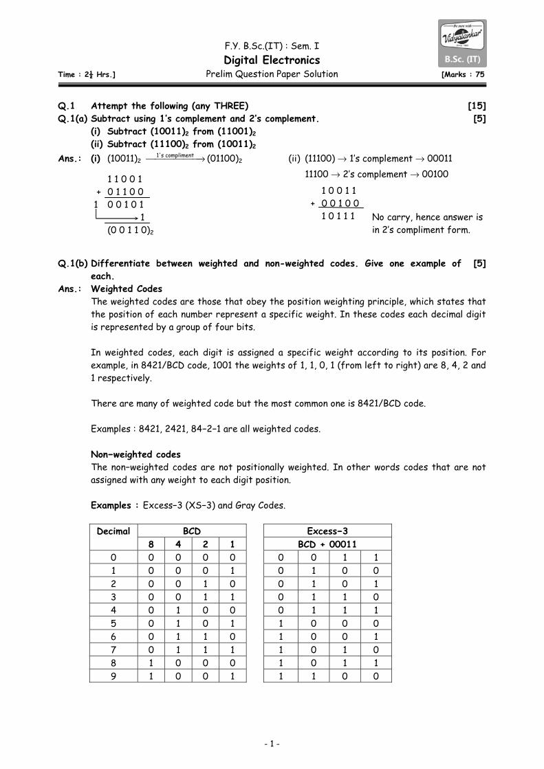
Ans.: Weighted Codes The weighted codes are those that obey the position weighting principle, which states that
the position of each number represent a specific weight. In these codes each decimal digit is represented by a group of four bits.
In weighted codes, each digit is assigned a specific weight according to its position. For
example, in 8421/BCD code, 1001 the weights of 1, 1, 0, 1 (from left to right) are 8, 4, 2 and 1 respectively.
There are many of weighted code but the most common one is 8421/BCD code. Examples : 8421, 2421, 84−2−1 are all weighted codes. Non−weighted codes The non−weighted codes are not positionally weighted. In other words codes that are not
assigned with any weight to each digit position. Examples : Excess−3 (XS−3) and Gray Codes.
Decimal BCD Excess−3 8 4 2 1 BCD + 00011
0 0 0 0 0 0 0 1 1 1 0 0 0 1 0 1 0 0 2 0 0 1 0 0 1 0 1 3 0 0 1 1 0 1 1 0 4 0 1 0 0 0 1 1 1 5 0 1 0 1 1 0 0 0 6 0 1 1 0 1 0 0 1 7 0 1 1 1 1 0 1 0 8 1 0 0 0 1 0 1 1 9 1 0 0 1 1 1 0 0
1 1 0 0 1 + 0 1 1 0 0 1 0 0 1 0 1 1 (0 0 1 1 0)2
1 0 0 1 1 + 0 0 1 0 0 1 0 1 1 1 No carry, hence answer is
in 2’s compliment form.
Vidyalankar : F.Y. B.Sc. (IT) DE
- 2 -
Q.1(c) Convert : (i) (24)10 ( )2 (ii) (36)16 ( )10 (iii) (7555)8 ( )2 [5]Ans.: (i) (24)10 ( )2
(24)10 (11000)2 (ii) (36)16 ( )10 (36)16 (3 161) + (6 16) = 48 + 6 = (54)10 (iii) (7555)8 ( )2
7 5 5 5 111 101 101 101
= (111 101 101 101)2 Q.1(d) Convert : (i) (F148.A)16 = ( )2 (ii) (1101110110110110.11011)2 ( )16 [5]Ans.: (i) (F148.A)16 = ( )2
F 1 4 8 A 1111 0001 0100 1000 1010
(1111 0001 0100 1000.1010)2 (ii) (1101 1101 1011 0110.11011)2 ( )16
1101 1101 1011 0110 . 1101 1000 D D B 6 . D 8
= (DDB6 . D8)16
Q.1(e) Perform BCD addition : (i) (48)10 + (66)10 (ii) (632)10 + (278)10 [5]Ans.: (i) (48)10 + (66)10 (ii) (632)10 + (278)10 = (910)10 Q.1(f) (i) (10)10 ¸ (4)10 (ii) (DADA)16 + (BABA)16 [5]
Ans.: (i) (10)10 ¸ (4)10
48 0 1 0 0 1 0 0 0 66 0 1 1 0 0 1 1 0 1 0 1 0 1 1 1 0
Invalid BCD Invalid BCD
1 0 1 0 1 1 1 0 + 0 1 1 0 0 1 1 0 0 0 0 1 0 0 0 1 0 1 0 0 1 1 4
6 3 2 0 1 1 0 0 0 1 1 0 0 1 0 + 2 7 8 0 0 1 0 0 1 1 1 1 0 0 0 1 0 0 0 1 0 1 0 1 0 1 0
Invalid BCD Invalid BCD Invalid BCD
2 24 2 12 0 2 6 0 2 3 0 2 1 1 1
1 0 0 0 1 0 1 0 1 0 1 0 + 0 0 0 0 0 1 1 0 0 1 1 0 1 0 0 1 0 0 0 1 0 0 0 0
9 1 0
1 0 1 0 0 1 0 1 0 1 0 0 0 0 1 0

Prelim Question Paper Solution
- 3 -
(ii) (DADA)16 + (BABA)16
= (19594)16
Q.2 Attempt the following (any THREE) [15]Q.2(a) List down Boolean laws. [5]Ans.:
1. Law of Identity A = A A A
2. Commutative Law A.B = B . A A + B = B + A
3. Associative Law A. (B . C) = A . B . C A + (B + C) = A + B + C
4. Idempotent Law A . A = A A + A = A
5. Double Negative Law A = A 6. Complementary Law A . A = 0
A + A = 1 7. Law of Intersection A . 1 = A
A . 0 = 0 8. Law of Union A + 1 = 1
A + 0 = A 9. DeMorgan’s Theorem AB = A B
A B = AB 10. Distributive Law A . (B + C) = (A . B) + (A . C)
A + (BC) = (A + B) . (A + C) 11. Law of Absorption A . (A + B) = A
A + (AB) = A 12. Law of Common Identities A . A B = AB
A + AB = A + B Q.2(b) Write a short note on De Morgan’s Theorem. [5]Ans.: Statement 1 The negation of conjuction is the disjunction of the negations Or we can define that as “The
compliment of the product of 2 variables is equal to the sum of the compliments of individual variables”.
(AB) = A + B Statement 2 “The negation of disjunction is the conjuction of the negations” Or we can define that as
“The compliments of the sum of two variables is equal to the product of the compliment of each variable.”
(A + B) = AB The truth table for De Morgan’s first statement ((AB)−A+ B) is given below.
A B A B A.B (A.B) A+B 0 0 1 1 0 1 1 0 1 1 0 0 1 1 1 0 0 1 0 1 1 1 1 0 0 1 0 0
(DADA)16 = 1 1 0 1 1 0 1 0 1 1 0 1 1 0 1 0(BABA)16 = 1 0 1 1 1 0 1 0 1 0 1 1 1 0 1 00 0 0 1 1 0 0 1 0 1 0 1 1 0 0 1 0 1 0 0
1 9 5 9 4

Vidyalankar : F.Y. B.Sc. (IT) DE
- 4 -
The truth table for De Morgan second statement ((A + B) − AB) is given below. A B A B A+B (A+B) A.B 0 0 1 1 0 1 1 0 1 1 0 1 0 0 1 0 0 1 1 0 0 1 1 0 0 1 0 0
Q.2(c) Implement of AND gate and OR gate using universal gates. [5]Ans.: Implementing AND using only NAND gates An AND gate can be replaced by NAND gates as shown in the figure (The AND is replaced
by a NAND gate with its output complemented by a NAND gate inverter)
Implementing OR using only NAND gates An OR gates can be replaced by a NAND gates as shown in the figure (The OR gate is
replaced by a NAND gate with all its inputs complemented by NAND gate inverters).
One NOR input pin is connected to the input signal A while all other input pins are connected
to logic 0. The output will be A.
Implementing OR using only NOR gates An OR gate can be replaced by NOR gates as shown in the figure (The OR is replaced by a
NOR gate with its output complemented by a NOR gate inverter)
Q.2(d) Reduce using Boolean law :
(i) A BC AB ABC (ii) ABC + ABC + ABC ABC ABC ABC ABC
[5]
Ans.: (i) A BC AB ABC
A BC A B A B C ABC B 1 A A C ABC A B C A A B C A B B A B C C A B C

Prelim Question Paper Solution
- 5 -
(ii) ABC + ABC + ABC ABC ABC ABC ABC = AB C C AB C C AB C C = AB + AB AB = AB + B A A = AB + B = A + B Q.2(e) Implement following function using Kmap :
F(A, B, C, D) = M (0, 1, 2, 4, 8, 10, 11, 15) + d (3, 9) [5]
Ans.: Y = B ACD + ACD Q.2(f) What are disadvantages of k-map? Explain the Q- M method. Discuss the terms
'prime impeccant', 'code word' and 'reduction table'. [5]
Ans.: Disadvantages of Kmap : (i) There is no guarantee that the kmap will give the best realization. By mistake you can
form redundant group. (ii) To deal with kmap for variable more than or equal to 6 is very difficult. (iii) Nowadays it is tend that we expect that everything should be done by computer. The
same way we except computer should reduce or minimize the gives expression, either by Boolean or kmap. But as no unique recognizable pattern is generated, while solving a kmap, it is not possible to write an algorithm.
Because of these problems associated with kmap, we use new method i.e. Quine Mc
Cluskey method. It is an efficient tabular method employed to minimize an expression for six or more
variables. Just like kmaps it searches for terms that cancel out the terms like A + A , x + x and so on.
Prime Implicant : An implicant p of f is called prime implicant if any product term obtained
by detecting a literal from p is not an implicant of f. Prime implicant is an indivisible implicant in that is ceases to be implicant if any of its literals are removed.
Code Word : In QM method, a product term X1, X2 ……Xn when n is equal to number of input
variable is represented by word of length. In that, 1 in the position denotes uncomplemented literal Xi, ‘0’ denotes complemented literal ( iX ) and (X) don’t care symbol indicates neither Xi nor iX . These words are called code codes.
Reduction Table : In QM method, we group minterms in Table format, based on number of
logical ‘1’s in the standard SOP term. Start from top and go on comparing minterms with remaining minterms from each
successive group.
AB CD CD CD CD CD
AB 1 1 X 1 0 1 3 2
AB 1 0 0 0 4 5 7 6
AB 0 0 1 0 12 13 15 14
AB 1 X 1 1 8 9 11 10

Vidyalankar : F.Y. B.Sc. (IT) DE
- 6 -
Combine the minterms such that they differ by only one bit. The bit that differs is replaced by ‘X’.
This table obtained by above process is known as 1st reduction table. Q.3 Attempt the following (any THREE) : [15]Q.3(a) Write short note on Full adder. [5]Ans.: An half-adder has only two inputs and there is no provision to add a carry coming from the
lower order bits when the multibit addition is performed. For this purpose, a third input (Cin) is added and this circuit is used to add A, B and Cin.
Table : Truth table for full-adder
Inputs Outputs
A B Cin Carry Sum 0 0 0 0 0 0 0 1 0 1 0 1 0 0 1 0 1 1 1 0 1 0 0 0 1 1 0 1 1 0 1 1 0 1 0 1 1 1 1 1
Fig. : Block schematic of full-adder K-map simplification for carry and sum :
Logic Diagram :
Fig. : Sum of product implementation of full-adder The Boolean function for sum can be further simplified as follows : Sum = in inin inAB C AB C AB C AB C
= ininC AB AB C AB AB
= ininC A B C A B
= in inC A B C A B
= inC A B

Prelim Question Paper Solution
- 7 -
With this simplified Boolean function circuit for full-adder can be implemented as shown in below figure.
Fig. : Implementation of full-adder A full-adder can also be implemented with two half-adders and one OR gate, as shown in
below figure. The sum output from the second half-adder is the exclusiveOR of Cin and the output of the first half-adder, giving
Sum = inC A B =
inC AB AB
= ininC AB AB C AB AB = ininC AB AB C AB AB
= in inC A B A B C AB AB
= ininC AB AB C AB AB
= inin in inAB C AB C AB C AB C
= in inin inAB C AB C AB C AB C and the carry output is Cout =
inAB C AB AB
= in inAB AB C AB C
= in in inAB C 1 AB C ABC Cin 1 = 1
= in in inAB C AB ABC ABC
= in inAB AC B B ABC
= in inAB AC ABC
= in in inAB C 1 AC ABC Cin + 1 = 1
= in in inABC AB AC ABC
= in inAB AC BC A A
= in inAB AC BC
Fig. : Implementation of a full-adder with two half-adders and an OR gate

Vidyalankar : F.Y. B.Sc. (IT) DE
- 8 -
Q.3(b) Write short not on Half adder. [5]Ans.: Truth Table :
A B SUM CARRY0 0 0 0 0 1 1 0 1 0 1 0 1 1 0 1
Kmap for SUM SUM = AB + AB K-map for CARRY : CARRY = AB Q.3(c) Design BCD to Excess 3. [5]Ans.: Excess-3 code is a modified form of a BCD number. The Excess-3 code can be derived from
the natural BCD code by adding 3 to each coded number. For example, decimal 12 can be represented in BCD as 0001 0010. Now adding 3 to each digit we get Excess 3 code as 0100 0101 (12 in decimal). With this information the truth table for BCD to Excess - 3 code converter can be determined as shown in Table.
Decimal B3 B2 B1 B0 E3 E2 E1 E0 0 0 0 0 0 0 0 1 1 1 0 0 0 1 0 1 0 0 2 0 0 1 0 0 1 0 1 3 0 0 1 1 0 1 1 0 4 0 1 0 0 0 1 1 1 5 0 1 0 1 1 0 0 0
A B
0
1
0 0
1
1 2
1 3
AB
0
1
0 0
1 1
1 1 2
3
AB
AB
A B

Prelim Question Paper Solution
- 9 -
6 0 1 1 0 1 0 0 1 7 0 1 1 1 1 0 1 0 8 1 0 0 0 1 0 1 1 9 1 0 0 1 1 1 0 0
K-map Simplification :
Logic Diagram :
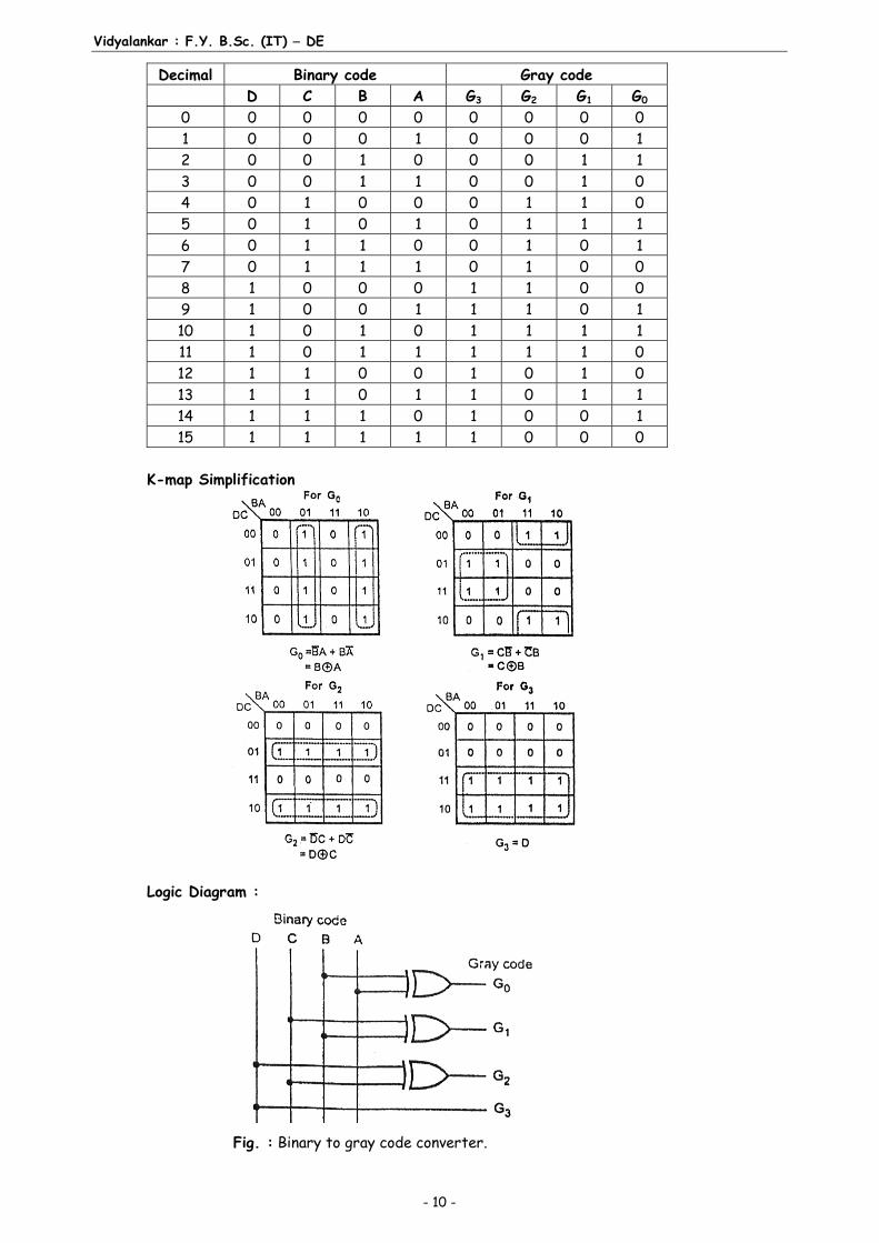
Fig. : BCD to Excess-3 code converter Q.3(d) Design convertor for 4 bit binary to 4 bit gray. [5]Ans.: The Gray code is often used in digital systems because it has the advantage that only one bit in
the numerical representation changes between successive numbers. Below table shows decimal and Binary codes and corresponding Gray code.
Vidyalankar : F.Y. B.Sc. (IT) DE
- 10 -
Decimal Binary code Gray code D C B A G3 G2 G1 G0
0 0 0 0 0 0 0 0 0 1 0 0 0 1 0 0 0 1 2 0 0 1 0 0 0 1 1 3 0 0 1 1 0 0 1 0 4 0 1 0 0 0 1 1 0 5 0 1 0 1 0 1 1 1 6 0 1 1 0 0 1 0 1 7 0 1 1 1 0 1 0 0 8 1 0 0 0 1 1 0 0 9 1 0 0 1 1 1 0 1 10 1 0 1 0 1 1 1 1 11 1 0 1 1 1 1 1 0 12 1 1 0 0 1 0 1 0 13 1 1 0 1 1 0 1 1 14 1 1 1 0 1 0 0 1 15 1 1 1 1 1 0 0 0
K-map Simplification
Logic Diagram :
Fig. : Binary to gray code converter.

Prelim Question Paper Solution
- 11 -
Gray Code to Binary Code Converter Table below shows the truth table for gray code to binary code converter. Table : Truth table for gray code to binary code converter
Gray code Binary code G3 G2 G1 G0 D C B A 0 0 0 0 0 0 0 0 0 0 0 1 0 0 0 1 0 0 1 1 0 0 1 0 0 0 1 0 0 0 1 1 0 1 1 0 0 1 0 0 0 1 1 1 0 1 0 1 0 1 0 1 0 1 1 0 0 1 0 0 0 1 1 1 1 1 0 0 1 0 0 0 1 1 0 1 1 0 0 1 1 1 1 1 1 0 1 0 1 1 1 0 1 0 1 1 1 0 1 0 1 1 0 0 1 0 1 1 1 1 0 1 1 0 0 1 1 1 1 0 1 0 0 0 1 1 1 1
K-map Simplification : A = 3 2 1 0 3 2 12 3 3 2 0G G G G G G G G G G G G + 3 2 3 2 02 3 1 0 3 2 1G G G G G G G G G G G G
= 1 0 13 2 3 2 0G G G G G G G G + 03 2 1 0 3 2 1G G G G G G G G
= 1 0 1 03 2 1 0 3 2 0 1G G G G G G G G G G G G
= 3 2 1 n 3 2 1 0G G G G G G G G
= 3 2 1 0 3 2 1 0G G G G G G G G
= 3 2 1 0G G G G
B = 3 2 3 2 13 2 1 2 3G G G G G G G G G G = 13 2 1 3 2G G G G G G
= 13 2 1 3 2G G G G G G
= 3 2 1G G G

Vidyalankar : F.Y. B.Sc. (IT) DE
- 12 -
C = 3 22 3G G G G D = G3
= 3 2G G Logic Diagram :
Fig. : Gray code to binary code converter BCD-to-Gray Code Converter Table below shows truth table for BCD to gray code converter Table : Truth table for BCD to gray code converter
BCD code Gray code
B3 B2 B1 B0 G3 G2 G1 G0
0 0 0 0 0 0 0 0
0 0 0 1 0 0 0 1
0 0 1 0 0 0 1 1
0 0 1 1 0 0 1 0
0 1 0 0 0 1 1 0
0 1 0 1 0 1 1 1
0 1 1 0 0 1 0 1
0 1 1 1 0 1 0 0
1 0 0 0 1 1 0 0
1 0 0 1 1 1 0 1

Prelim Question Paper Solution
- 13 -
K-map Simplification :
Logic Diagram :
Fig. : BCD to gray code converter. Q.3(e) Design 2 bit magnitude comparator. [5]Ans.: The truth table for 2-bit comparator is given in table.
Inputs Outputs A A B B A > B A = B A < B 0 0 0 0 0 1 0 0 0 0 1 0 0 1 0 0 1 0 0 0 1 0 0 1 1 0 0 1 0 1 0 0 1 0 0 0 1 0 1 0 1 0 0 1 1 0 0 0 1 0 1 1 1 0 0 1 1 0 0 0 1 0 0 1 0 0 1 1 0 0 1 0 1 0 0 1 0 1 0 1 1 0 0 1 1 1 0 0 1 0 0 1 1 0 1 1 0 0 1 1 1 0 1 0 0 1 1 1 1 1 1 0

Vidyalankar : F.Y. B.Sc. (IT) DE
- 14 -
K-map Simplification :
Y(A = B) = 1 0 1 0 1 0 1 0 1 0 1 0 1 0 1 0AA BB AA BB AA BB AA BB
= 1 1 0 0 0 0 1 1 0 0 0 0AB (A B A B ) AB (A B A B )
= 0 0 1 1A B A B
Y (A < B) = 1 0 0 0 1 0 1 1AA B A BB AB
Logic Diagram
Q.3(f) Design BCD Adder using IC 7843. [5]Ans.: The output of combinational circuit should be 1 if the sum produced by adder 1 is greater
than 9 i.e. 1001. The truth table is as follows :
Y(A >

Prelim Question Paper Solution
- 15 -
Write K−map : For Y output
The Boolean expression is, Y = S3S2 + S3S1
Q.4 Attempt the following (any THREE) [15]Q.4(a) Write short note on Master−slave JK flip flop. [5]Ans.: Master−slave JK flip flop The Master−slave flip−flop basically a combination of two JK flip−flops connected together
in a series configuration. Out of these, one acts as the “master” and the other as a “slave”. The output from the master flip flop is connected to the two inputs of the slave flip flop whose output is fed back to inputs of the master flip flop.
In addition to these two flip−flops, the circuit also includes an inverter. The inverter is connected to clock pulse in such a way that the inverted clock pulse is given to the slave flip−flop. In other words if CP = 0 for a master flip−flop, then CP = 1 for a slave flip−flop and if CP = 1 for master flip flop then it becomes 0 for slave flip flop.

Vidyalankar : F.Y. B.Sc. (IT) DE
- 16 -
Working (i) When the clock pulse goes to 1, the slave is isolated; J and K inputs may affect the
state of the system. The slave flip−flop is isolated until the CP goes to 0. When the CP goes back to 0, information is passed from the master flip−flop to the slave and output is obtained.
(ii) Firstly the master flip flop is positive level triggered and the slave flip flop is negative level triggered, so the master responds before the slave.
(iii) If J = 0 and K = 1, the high ‘Q’ output of the master goes to the K input of the slave and the clock forces the slave to reset, thus the slave copies the master.
(iv) If J = 1 and K = 0, the high Q output of the master geos to the J input of the slave and the Negative transition of the clock sets the slave, copying the master.
(v) If J = 1 and K = 1, it toggles on the positive transition of the clock and thus the slave toggles on the negative transition of the clock.
(vi) If J = 0 and K = 0, the flip flop is disabled and Q remains unchanged. Timing Diagram of a Master flip flop
Q.4(b) Implement following function using 16:1 Mux F(A, B, C, D) = m(0, 1, 6, 7, 10,
11, 14, 15) [5]
Ans.:
D0
D1
D2
D3
D4
D5
D6
D7
D8
D9
D10
D11
D12
D13
D14
D15
S3 S2 S1 S0
16 : 1 MUX
y Output
Select line
Logic − 1
Logic − 0

Prelim Question Paper Solution
- 17 -
Q.4(c) Draw symbol, circuit and truth table of JK flip flop. [5]Ans.:
Truth Table
Input Output Description J K Q Q 0 0 0 0 Memory no change 0 0 0 1 0 1 1 0 Reset Q = 0 0 1 0 1 1 0 0 1 Set Q = 1 1 0 1 0 1 1 0 1 Toggle 1 1 1 0
Q.4(d) Describe with a truth table the working of 4:1 Mux. [5]Ans.: A 4 to 1 multiplexer consists four data input lines as D0 to D3, two select lines as S0 and S1
and a single output line Y. The select lines S0 and S1 select one of the four input lines to connect the output line. The particular input combination on select lines selects one of input (D0 through D3) to the output.
The figure below shows the block diagram of a 4 to 1 multiplexer in which the multiplexer
decodes the input through select line.
The truth table of a 4 to 1 multiplexer is shown below in which four input combinations 00,
10, 01 and 11 on the select lines respectively switches the inputs D0, D2, D1 and D3 to the output. That means when S1 = 0 and S0 = 0, the output at Y is D0, similarly Y is D1 if the select inputs S1 = 0 and S0 = 1 and so on.
Select Data Inputs Output S1 S0 Y 0 0 D0
0 1 D1 1 0 D2
Vidyalankar : F.Y. B.Sc. (IT) DE
- 18 -
1 1 D3
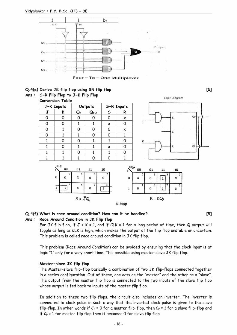
Q.4(e) Derive JK flip flop using SR flip flop. [5]Ans.: S−R Flip Flop to J−K Flip Flop Conversion Table
J−K Inputs Outputs S−R Inputs J K QP QP+1 S R 0 0 0 0 0 x 0 0 1 1 x 0 0 1 0 0 0 x 0 1 1 0 0 1 1 0 0 1 1 0 1 0 1 1 x 0 1 1 0 1 1 0 1 1 1 0 0 1
Q.4(f) What is race around condition? How can it be handled? [5]Ans.: Race Around Condition in JK Flip flop For JK flip flop, if J = K = 1, and if CLK = 1 for a long period of time, then Q output will
toggle as long as CLK is high, which makes the output of the flip flop unstable or uncertain. This problem is called race around condition in JK flip flop.
This problem (Race Around Condition) can be avoided by ensuring that the clock input is at
logic “1” only for a very short time. This possible using master slave JK flip flop. Master−slave JK flip flop The Master−slave flip−flop basically a combination of two JK flip−flops connected together
in a series configuration. Out of these, one acts as the “master” and the other as a “slave”. The output from the master flip flop is connected to the two inputs of the slave flip flop whose output is fed back to inputs of the master flip flop.
In addition to these two flip−flops, the circuit also includes an inverter. The inverter is
connected to clock pulse in such a way that the inverted clock pulse is given to the slave flip−flop. In other words if CP = 0 for a master flip−flop, then CP = 1 for a slave flip−flop and if CP = 1 for master flip flop then it becomes 0 for slave flip flop.
S = PJQ R = KQP

Prelim Question Paper Solution
- 19 -
Q.5 Attempt the following (any THREE) [15]Q.5(a) Write short note on SISO shift register. [5]Ans.: The input to this register is given in serial fashion i.e. one bit after the other through a single
data line and the output is also collected serially. The data can be shifted only left or shifted only right. Hence it is called Serial in Serial out shift register or a SISO shift register.

Vidyalankar : F.Y. B.Sc. (IT) DE
- 20 -
Q.5(b) Design MOD 10 counter. [5]Ans.: MOD 10 asynchronous counter counts from 0000 to 1001. Rest of the states are invalid. To
design the combinational circuit of valid states, following truth table and K−map is drawn : QD QC QB QA Reset
logic 0 0 0 0 1 0 0 0 1 1 0 0 1 0 1 0 0 1 1 1 0 1 0 0 1 0 1 0 1 1 0 1 1 0 1 0 1 1 1 1 1 0 0 0 1 1 0 0 1 1 1 0 1 0 0 1 0 1 1 0 1 1 0 0 0 1 1 0 1 0 1 1 1 0 0 1 1 1 1 0
Table: Truth table for MOD 10 asynchronous counter
Q.5(c) Write short not on Ring Counter. [5]Ans.: Ring Counter A ring counter is a type of counter composed of flip−flops connected into a shift register,
with the output of the last flip−flop fed to the input of the first, making a “circular” or “ring” structure.
Truth table
State Q0 Q1 Q2 Q3 0 1 0 0 0 1 0 1 0 0 2 0 0 1 0
TA QA
Reset
CLK
TB
AQ BQReset
QB TC
CQReset
QC
1 1 1
TD
DQReset
QD
1
K−maps
QB QA
QDQC 00 01 11 10
00 1 0 1 1 1 3 1 2 01 1 4 1 5 1 7 1 6 11 0 12 0 13 0 15 0 14
10 1 8 1 9 0 11 0 10
y = D C BQ Q Q
Fig.: K−map for above truth table

Prelim Question Paper Solution
- 21 -
3 0 0 0 1 0 1 0 0 0 1 0 1 0 0 2 0 0 1 0 3 0 0 0 1 0 1 0 0 0
Waveform
Q.5(d) Design Asynchronous 3−bit Up counter. [5]Ans.: (Mod − 7, 0−1−2−3−4−5−6−7)
T QA
AQ
T QB
BQ
QA
T QC
CQ
QB QC
CLK
Logic (1)
0 0 1 0 1 0 1 0 1 0 1
0 0 1 1 0 0 1 1 0 0 1 1
0 0 0 0 1 0 0 0 0 1 1 1
QC QB QA 0000 0011 0102 0113 1004 1015 1106 1117 0000 0011 0102
1 2 3 4 5 6 7

Vidyalankar : F.Y. B.Sc. (IT) DE
- 22 -
Q.5(e) Design Mod−6 counter. [5]Ans.: Mod − 6 0 1 2 3 4 5
QC QB QA Y 0 0 0 1 0 0 0 1 1 1 0 1 0 1 2 0 1 1 1 3 1 0 0 1 4 1 0 1 1 5 1 1 0 0 6 1 1 1 0 7
Y = BQC Q Q.5(f) Design 2 bit Synchronous Up counter. [5]Ans.:
TB = m (1, 3) TA = m (0, 1, 2, 3)
QBQA
QC
B AQ Q
B AQ Q
QBQA
QB AQ
QC 1 1 1 1 0 1 3 2
QC 1 1 0 0 4 5 7 6
TA QA
Reset
TB
AQ BQReset
QB TC
CQ Reset
QC
Logic 1
QB QA QB+1 QA + 1 TB TA 0 0 0 1 0 1
0 1 1 0 1 1
1 0 1 1 0 1
1 1 0 0 1 1
0
1
2
3
1
2
3
0
(0)
(1)
(2)
(3)
QA QB
AQ
QA
BQ 1 1 0 1
QB 1 1 2 3
TA = 1
QA
QB
AQ
QA
BQ 0 1 0 1
QB 0 1 2 3
TB = QA
TA QA
AQ
CLK
Logic 1
Tb QB
BQ
Output