functional triple modular redundancy (ftmr) - cobham … · · 2012-07-17triple modular...
TRANSCRIPT
FPGA-003-01Version 0.2
December 2002
Stora Nygatan 13 tel +46 31 802405411 08 Göteborg fax +46 31 802407Sweden www.gaisler.com
EUROPEAN SPACE AGENCY CONTRACT REPORTThe work described in this report was done under ESA contract, No. 15102/01/NL/FM(SC) CCN-3.
Responsibility for the contents resides in the author or organisation that prepared it.
Functional Triple Modular Redundancy (FTMR) VHDL Design Methodology for Redundancy in Combinatorial and Sequential Logic
Design and Assessment Report
Prepared by Sandi Habinc

FPGA-003-01 2
Table of contents
1 INTRODUCTION ......................................................................................... 41.1 Scope.............................................................................................................. 41.2 Background .................................................................................................... 41.3 Acronyms and abbreviations.......................................................................... 41.4 Reference document....................................................................................... 5
2 SINGLE EVENT UPSET MITIGATION TECHNIQUES ........................... 62.1 Triple Module Redundancy (TMR) ............................................................... 62.2 Module level mitigation ................................................................................. 72.3 Gate level mitigation...................................................................................... 8
3 A VHDL APPROACH TO COMBINATORIAL AND SEQUENTIAL TMR 93.1 The architecture.............................................................................................. 93.2 Configuration options .................................................................................... 103.3 Methodology issues........................................................................................ 113.3.1 Input and output ............................................................................................. 113.3.2 Bus holders..................................................................................................... 113.3.3 Re-use of old VHDL code ............................................................................. 113.3.4 Configuration memory................................................................................... 113.3.5 Refresh of TMR structures............................................................................. 113.3.6 Required level of redundancy ........................................................................ 123.3.7 Template based approach............................................................................... 123.3.8 Synthesis tools................................................................................................ 12
4 VHDL CODE STRUCTURE ........................................................................ 134.1 Triple Modular Redundancy D-Type Flip-Flop............................................. 144.2 Interface package ........................................................................................... 154.2.1 Definitions for non-redundant clock and reset interfaces .............................. 154.2.2 Definitions for non-redundant input / output interfaces................................. 154.3 Redundancy package...................................................................................... 164.3.1 Definition of range for Triple Modular Redundancy..................................... 164.3.2 Definitions for clock and reset interfaces ...................................................... 164.3.3 Definitions for input / output interfaces ......................................................... 164.3.4 Conversion from bit to integer for generics ................................................... 174.3.5 Component declaration for generic Triple Modular Redundancy flip-flop ... 174.4 Entity of the module....................................................................................... 184.4.1 Generic clause ................................................................................................ 184.4.1.1 Redundancy configuration ............................................................................. 184.4.1.2 Functionality configuration............................................................................ 184.4.2 Port clause ...................................................................................................... 194.4.2.1 Clock and reset interface................................................................................ 194.4.2.2 Input interface ................................................................................................ 194.4.2.3 Output interface.............................................................................................. 19

FPGA-003-01 3
4.5 Architecture of the module ............................................................................ 204.5.1 Declarative part .............................................................................................. 204.5.1.1 Definition of private types, constants and subprograms ................................ 204.5.1.2 Definition of types for sequential elements ................................................... 204.5.1.3 Definition of type for combinatorial elements ............................................... 214.5.1.4 Declaration of reset values ............................................................................. 214.5.1.5 Conversion from record to array of bits......................................................... 224.5.1.6 Conversion from array of bits to record......................................................... 234.5.1.7 Support functions ........................................................................................... 244.5.1.8 Declaration of vector types and signals ......................................................... 254.5.1.9 Definition of combinatorial behaviour........................................................... 254.5.1.9.1User defined inputs ........................................................................................ 254.5.1.9.2Pre-defined input and outputs ........................................................................ 264.5.1.9.3Pre-defined variables...................................................................................... 264.5.1.9.4Definition of unregistered variables............................................................... 264.5.1.9.5Pre-defined registered variable ...................................................................... 274.5.1.9.6Definition of combinatorial logic................................................................... 274.5.1.9.7Synchronous reset .......................................................................................... 284.5.1.9.8pre-defined variables converted to signals..................................................... 284.5.2 Statement part ................................................................................................ 284.5.2.1 Combinatorial behaviour................................................................................ 284.5.2.2 Output ports.................................................................................................... 294.5.2.3 Sequential behaviour...................................................................................... 294.5.2.3.1Sequential behaviour with explicit flip-flop instances................................... 294.5.2.3.2Sequential behaviour with inferred flip-flops ................................................ 304.6 Graphical overview of the FTMR approach .................................................. 31
5 RESULTS FROM A SIMPLE APPLICATION............................................ 32
6 RESULTS FROM A DEMONSTRATION APPLICATION ....................... 33
7 CONCLUSIONS............................................................................................ 35
APPENDIX A: VHDL CODE................................................................................... 36A.1 TMR D-Type Flip-Flop ................................................................... 36A.2 Interface package ............................................................................. 43A.3 Redundancy package ....................................................................... 44A.4 Pseudo-Randomiser ......................................................................... 46A.5 Xilinx entities and architectures (not necessary for synthesis)........ 54A.6 Xilinx specific triple redundancy voter............................................ 55

FPGA-003-01 4
1 INTRODUCTION
1.1 Scope
This document discusses the use of Triple Modular Redundancy (TMR) for the protection ofcombinatorial and sequential logic in reprogrammable logic devices. A VHDL approach hasbeen developed for automatic TMR insertion and a demonstration design has been developed.The approach is called “Functional Triple Modular Redundancy (FTMR)”.
This document addresses the protection of random sequential and combinatorial logic. Thisdocument does not address the protection of inputs and outputs, the usage of on-chip blockmemories or dedicated shift-registers etc. It assumes a good knowledge of the Xilinxarchitecture. For detailed information on Xilinx FPGAs and mitigation techniques such asconfiguration memory scrubbing, see [RD7].
1.2 Background
Field Programmable Gate Array (FPGA) devices have been used in space for more than adecade with a mixed level of success. Until now, few reprogrammable devices have been usedon spacecraft due to their sensitivity to involuntary reconfiguration due to Single Event Upsets(SEU) induced by radiation. But with the advent of reprogrammable devices featuring a millionsystem gates or more, it is not longer feasible to disregard these technologies.
Triple Modular Redundancy (TMR) has traditionally been used for protecting digital logic fromthe SEUs in space born applications. The main usage has been either on module level or for theprotection of sequential elements in digital logic. With the use of reprogrammable logic, suchas Static Random Access Memory (SRAM) based FPGAs, the protection of the sequential logicis insufficient since the logical functionality of the FPGA can be changed due to a chargedparticle hitting the on-chip configuration SRAM. Protection of the combinatorial logic istherefore required to avoid involuntary changes of functionality.
Several approaches have been made to solve this problem, most based on modular replicationand voting. These approaches have the advantage of detecting a large range of errors, but havethe disadvantage of not being able to restore the sequential state of the module that has beenaffected. A better approach is to perform TMR on the gate level. This has previously been donefor the sequential elements, but not until recently has it been considered for the combinatoriallogic as well, as will be discussed in this report.
1.3 Acronyms and abbreviations
FPGA Field Programmable Gate ArrayFTMR Functional Triple Modular RedundancySEU Single Event UpsetSRAM Static Random Access MemoryTMR Triple Modular RedundancyVHDL VHSIC Hardware Description LanguageVHSIC Very High Speed Integrated Circuits

FPGA-003-01 5
1.4 Reference document
RD1 Triple Module Redundancy Design Techniques for Virtex FPGAs, Application Note:Virtex Series, XAPP197 (v1.0) November 2001, Xilinx Inc.
RD2 Radiation Characterization, and SEU Mitigation, of the Virtex FPGA for Space-BasedReconfigurable Computing, E. Fuller et al., 2000 IEEE NSREC, October 2000
RD3 Radiation Testing Update, SEU Mitigation, and Availability Analysis of the VirtexFPGA for Space Reconfigurable Computing, E. Fuller et al., 2000 MAPLD, JohnsHopkins University, Laurel, Maryland, USA, September 2000
RD4 SEU Mitigation Techniques for Virtex FPGAs in Space Applications, C. Carmichaelet al., 1999 MAPLD, Johns Hopkins University, Laurel, Maryland, USA, September1999
RD5 Reliability of Programmable Input/Output Pins in the Presences of ConfigurationUpsets, N. Rollins et al., 2002 MAPLD, Johns Hopkins University, Laurel, Maryland,USA, September 2002
RD6 Single-Event Upsets in SRAM FPGAs, M. Caffrey et al., 2002 MAPLD, JohnsHopkins University, Laurel, Maryland, USA, September 2002
RD7 Suitability of reprogrammable FPGAs in space applications, S. Habinc, FPGA-002-01,Version 0.4, September 2002, Gaisler Research, Sweden
RD8 CCSDS Unsegmented Code (CUC) & CCSDS Time Manager (CTM) SynthesizableVHDL Cores Data Sheet, ESA D/TOS-ESM/SH/154, Issue 0.1 Rev. A, Nov. 2000

FPGA-003-01 6
2 SINGLE EVENT UPSET MITIGATION TECHNIQUES
2.1 Triple Module Redundancy (TMR)
A commonly known method for SEU mitigation is Triple Module Redundancy (TMR) withvoting. This mitigation scheme uses three identical logic circuits performing the same task inparallel with corresponding outputs being compared through a majority voter circuit. The mostcommon example of TMR is a d-type flip-flop that has been triplicated and to which a voter hasbeen added on its output. By replacing all flip-flops in design with the circuit shown in figure 1,one would protect the design against SEUs in the flip-flops. However, this would not protectagainst SEUs in the combinatorial logic connecting the flip-flops in the design.
Figure 1: Triple Modular Redundancy with voting
The effects of SEUs are not confined to the registers in digital designs, but are also present inthe combinatorial logic for which there are several protection schemes proposed. Theseschemes mostly deal with transient glitches in the combinatorial logic that could result in upsetsin the sequential elements. This should not be confused with what will be discussed next.
The subject SRAM-based FPGAs are not only susceptible to SEUs in the user registers but alsoin the configuration SRAM memory itself. The effect of an SEU is in this case much moredifficult to predict since it can effect the logical function of the design, not only its sequentialstate as protected in figure 1. This calls for a protection technique that covers the complete logicof the design, both the sequential and combinatorial part.
Note that it is not sufficient to update the configuration SRAM memory continuously to removeany bit errors induced by SEUs, since the effect of the configuration change will change thelogic which in turn will potentially lead to the change of the internal state of the design, i.e. thestate of the various registers and flip-flops. By correcting the configuration SRAM memory, onecan repair the logic, but not re-establish the state of the design.
D Q
D Q
D Q
outputinput
FPGA-003-01 7
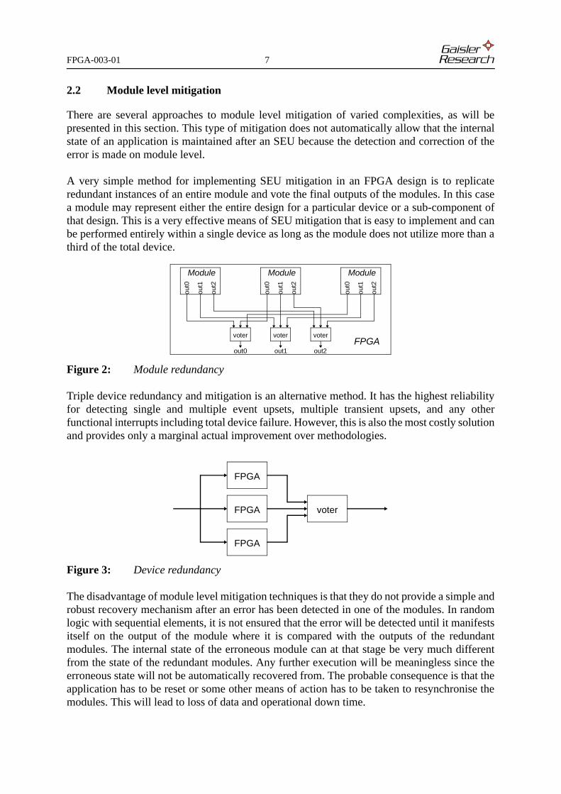
2.2 Module level mitigation
There are several approaches to module level mitigation of varied complexities, as will bepresented in this section. This type of mitigation does not automatically allow that the internalstate of an application is maintained after an SEU because the detection and correction of theerror is made on module level.
A very simple method for implementing SEU mitigation in an FPGA design is to replicateredundant instances of an entire module and vote the final outputs of the modules. In this casea module may represent either the entire design for a particular device or a sub-component ofthat design. This is a very effective means of SEU mitigation that is easy to implement and canbe performed entirely within a single device as long as the module does not utilize more than athird of the total device.
Figure 2: Module redundancy
Triple device redundancy and mitigation is an alternative method. It has the highest reliabilityfor detecting single and multiple event upsets, multiple transient upsets, and any otherfunctional interrupts including total device failure. However, this is also the most costly solutionand provides only a marginal actual improvement over methodologies.
Figure 3: Device redundancy
The disadvantage of module level mitigation techniques is that they do not provide a simple androbust recovery mechanism after an error has been detected in one of the modules. In randomlogic with sequential elements, it is not ensured that the error will be detected until it manifestsitself on the output of the module where it is compared with the outputs of the redundantmodules. The internal state of the erroneous module can at that stage be very much differentfrom the state of the redundant modules. Any further execution will be meaningless since theerroneous state will not be automatically recovered from. The probable consequence is that theapplication has to be reset or some other means of action has to be taken to resynchronise themodules. This will lead to loss of data and operational down time.
Module
out0
out1
out2
out0 out1 out2
voter voter voter
Module
out0
out1
out2
Moduleou
t0
out1
out2
FPGA
FPGA
FPGA
FPGA
voter

FPGA-003-01 8
2.3 Gate level mitigation
In [RD1], mitigation techniques are discussed from the architectural point of view for the XilinxVirtex technology. Emphasis is put on protecting the user logic on the gate-level. For furtherdiscussions, a distinction between combinatorial logic and sequential logic will be made.
Figure 4: Sequential and combinatorial logic
Since SEUs can affect both the sequential and the combinatorial logic, the combinatorial logicneeds to be made redundant as well. The importance of feeding back the voted result to all votedsequential elements is discussed in [RD1]. This is done to restore the state of all redundantsequential elements and to avoid error build up. The voting for the redundant combinatoriallogic can be performed after the sequential elements, before the sequential elements or throughout the combinatorial logic, depending on what level of protection that is required.
Figure 5: TMR for sequential and combinatorial logic at gate level
The advantage of gate level mitigation techniques is that the voting between different logicelements can take place between the sequential elements. The voted result is normally fed backto the sequential elements, avoiding that an error is propagated between sequential elements.The synchronisation between the redundant parts is thus maintained. This is because each erroris detected within a clock period and the state of the redundant parts will thus not differ for morethan a clock period. The rest of this report will discuss a gate level mitigation using high leveldescriptions in VHDL.
Figure 6: TMR for sequential, combinatorial and voter logic at gate level
combinatorial logic
sequential logic
sequential logic
sequential logic
combinatorial logic
sequential logic
vote
r
vote
r
combinatorial logic
vote
r
sequential logic
sequential logic
vote
r combinatorial logic
combinatorial logic
sequential logic
vote
r
vote
r
sequential logic
vote
r
vote
r
vote
r
combinatorial logicvote
r vo
ter
vote
r
sequential logic
vote
r vote
r vo
ter
vote
r

FPGA-003-01 9
3 A VHDL APPROACH TO COMBINATORIAL AND SEQUENTIAL TMR
While it is fairly simple to implement TMR for sequential elements alone, it is a challenge toimplement it in an efficient way for the combinatorial logic. The principles are fairly simple andit is not that difficult to implement them on the gate level with a schematic entry based designmethod. It is however difficult to do it using a high level design language such as VHDL andstill obtain the desired ease of use.
The ultimate situation is when the designer does not need to be concerned with the TMR aspectsat all, e.g. if automatically supported by the synthesis tool. Until then it is still possible todevelop a VHDL design style that allows itself to high level descriptions with little influence onthe actual work spent on describing the design functionality. An attempt to such an approach ispresented hereafter and is called Functional Triple Modular Redundancy (FTMR).
A code example is explained in detail in section 4 and is provided in its entire in appendix A.
3.1 The architecture
The architecture of Functional Triple Modular Redundancy (FTMR) is based on two mainelements; a sequential block and a combinatorial block, as shown in figure 7. This approach hasbeen used in other developments such as the LEON SPARC microprocessor where only thesequential block was protected by means of modular redundancy.
Figure 7: Sequential and combinatorial blocks in FTMR
The novelty of FTMR is however that both sequential and combinatorial blocks can beprotected by means of triple modular redundancy. The redundancy of the sequential block isstraight forward, since each flip-flop is implemented with a specific TMR d-type flip-flop whichwill be discussed later.
The redundancy for the combinatorial block is slightly more complicated since it requirestriplication of random logic that is less predictable than the flip-flops. This has been solved bydescribing the combinatorial logic in a procedure that can be instantiated multiple times in thecombinatorial block. This might seem simple, but it requires quite a few VHDL tricks in orderto establish the desired interconnections between the blocks, and to avoid having them removedby the synthesis tools during optimisation.
sequential block
combinatorial bock
input recordsoutput records
next state record
current state record
clock signals
reset signals

FPGA-003-01 10
The same approach has been taken for the communication between the two blocks as was donefor the LEON model. Record types in VHDL are used for describing ports going to and fromthe entity as well as for signals going between the blocks in the VHDL architecture. The recordtypes can be nested to group logically different categories of information, etc.
The sequential block has one input record signal and one output record signal, plus clock andreset inputs. The input record carries the next state of all the sequential elements, and the outputrecord carries the current state of all the sequential elements. In synchronous designs, the outputrecord signal is also fed to the output record ports of the entity.
The combinatorial block has several input record signals and two output record signal. Oneinput record carries the current state of the sequential elements, and one output record carriesthe next state of the sequential elements. Additional input record signals are used for connectingthe combinatorial block with the input ports of the entity. The second output record signalcarries combinatorial results that can be fed to the non-registered output record ports of theentity. The combinatorial block does not include any sequential elements and can thus also beused for describing purely combinatorial logic.
Since the record types can be of various subtypes and array structures, it is not possible to mapsuch a record directly and automatically to individual flip-flops by means of explicitinstantiation. Instead, the designer will have to define a function that maps the different recordelements to bits in an array, and a reverse function that maps bits from an array to the recordelements. The array type is then used for connecting the flip-flops to the record type. It is notpossible to utilise inference of flip-flops, since the flip-flop has to have some specificcharacteristics for redundancy purposes as will be discussed later. This is a weakness of themethod and VHDL since it requires work not related to the design of the functionality itself.
3.2 Configuration options
The FTMR approach allows a design to be implemented in several ways, with a varying levelof redundancy. The first configuration is the behavioural in which the sequential elements areimplemented by flip-flop inference by the synthesis tool. It does not allow redundancy.
In the structural configuration all sequential elements are implemented with explicitlyinstantiated TMR d-type flip-flops. This configuration can be used without redundancy, and itmust be used when redundancy is required. See figure 4.
The sequential configuration provides redundancy on the sequential elements only. It providesonly a single set of input and output ports for the entity, except for the clock and reset ports thatcan be triplicated. The triplicated sequential elements can be voted with a single output voterimplemented with random logic or as specific Xilinx tri-state buffers. See figure figure 1.
The combinatorial configuration is a super set of the sequential configuration, providingtriplication of all ports and all combinatorial logic. The triplicated sequential elements can bevoted with a single, see figure 5, or triplicated input and output voters, see figure 6,implemented with random logic or as specific Xilinx tri-state buffers. No explicit voting isprovided for the output ports of the actual module, since the voting occurs just before or afterthe flip-flops. For purely combinatorial logic, no voting occurs in the module, only triplicationof the logic, since it is assumed that the logic will end up at a flip-flop or that explicit voting willbe made for the outputs of the device.
FPGA-003-01 11
3.3 Methodology issues
3.3.1 Input and output
The FTMR approach currently only handles modules and not complete designs. The main partsmissing is the handling of the input and outputs of the device. There are several ways in whichthe input and outputs can be handled, all depending on what level of protection one requires.The simplest approach would be only to have a single external input that is connected to atriplicated input on the module level. The same could be done for the outputs, only connectingone of the triplicated outputs on the module to a single external output. Another straight forwardapproach is to triplicate all external inputs and outputs and to handle the voting outside thedevice. These issues have been left to the user to handle for the time being.
3.3.2 Bus holders
Several problems with so called bus holders, or half-latches, that are sensitive to upsets havebeen reported for the Xilinx Virtex technology. In the available documentation [RD6], severalcells that can be affected by this phenomena have been listed. In the synthesis results obtainedfor the two example applications discussed later in this document, no such cells have beenobserved. It is however unclear whether this is due to the coding style or if it can still occur. Oneshould always analyse the resulting netlist for potential bus holders.
3.3.3 Re-use of old VHDL code
It was shown during the design of the demonstration application that converting an existingdesign to the structure presented in the FTMR approach is feasible, provided that the originaldesign is described on a fairly high descriptive level. There is however definitely a learningthreshold that needs to be overcome to be able to design with FTMR.
3.3.4 Configuration memory
Although not discussed in this document in detail, it is assumed that the proposed FTMRapproach is combined with scrubbing of the configuration memory. The FTMR approach willonly protect the design from a single error in the configuration memory belonging to a specificfunction. A second error in the configuration memory affecting the same function could renderthe TMR protection inefficient. It is therefore necessary to provide continuous scrubbing of theconfiguration memory to avoid an error build up.
3.3.5 Refresh of TMR structures
As for all TMR structures, it is important that the flip-flops are refreshed continuously with newvoted values in order to avoid error build up. In the FTMR approach this is done automaticallysince all flip-flops are clock with the system clock. One should note that when using an externalsignal to clock flip-flops, one must be aware that the flip-flops will perhaps not be refreshedoften enough. The information from those flip-flops should therefore be moved to the systemclock domain as fast as possible, where the flip-flops are refreshed regularly.

FPGA-003-01 12
3.3.6 Required level of redundancy
The FTMR approach provides several levels of protection against upsets in the configurationmemory as well as in the sequential elements of the design. It is however not clear what levelof protection is actually required. This can only be derived from a characterisation of the FTMRapproach by means of irradiation. For example, it is not obvious how many voters are requiredaround a sequential element. The method allows from zero to three voters to be placed in frontand/or after the sequential element.
One could reason that only one voter after the flip-flop would be sufficient if implemented usingthe Xilinx specific tri-state buffer implementation. This is however not evident since the bufferstructure has more than the three required inputs, which could lead to corruption of functionalitydue to errors else were in the design, e.g. between the voter output and the flip-flop input. Tobring clarity to these issues, further analysis and test is required.
3.3.7 Template based approach
The FMTR approach is based on templates which the user can modify for each new module thatneed to be developed. To reduce the design effort, one could develop an simple pre-processoror VHDL code generator which could produce the VHDL code sections specifically needed forthe approach. This could cover the cumbersome conversion between record and array types thatwas discussed earlier. It could also cover the copying of input ports of the entity to the inputs ofthe combinatorial procedure, etc.
3.3.8 Synthesis tools
Although there are several different synthesis tools suitable for Xilinx devices, only one hasbeen used to assess the proposed methodology. Synplify from Synplicity Inc. was used as themain driver for the development of the method. Synplify was chosen due to availability. DesignCompiler from Synopsys Inc. was also used to assess the method to some extent.

FPGA-003-01 13
4 VHDL CODE STRUCTURE
The proposed Functional Triple Modular Redundancy (FTMR) approach is implemented inVHDL using a TMR based d-type flip-flop, two packages, and the entity and architecture of themodule to be implemented. FTMR is based on parts that are pre-defined in a template and partsthat need to be defined by the user for each new module that is being designed. This will behighlighted in the VHDL code example that is explained in detail in the following sections andthat is provided in its entire in appendix A.
An overview of the different VHDL objects and files used in the proposed approach is given infigure 8. A graphical overview of the approach is provided in figure 10 in section 4.6.
The VHDL code is based on VHDL IEEE Std 1076 - 1993, and is thus not directly backwardcompatible with Std 1076 - 1987, although this can be achieved with some minor modifications.
Figure 8: Overview of VHDL objects and file hierarchy
Interface package
Redudant package
BUFT
PullUp
Xilinx
TRV
TMR
Triple Redundancy Voter
Triple Modular RedundancyFlip-Flop
Combinatorial
Pack UnPack
Combinatorial
CombinatorialGen
StructuralGen
TMR
TMR
TMR
TMR
Combinatorial
Combinatorial
Pack
UnPack
generic declaration
port declaration
Module entity
Module architecture
architectural declaration
architectural statement

FPGA-003-01 14
4.1 Triple Modular Redundancy D-Type Flip-Flop
The basis for the FTMR approach is the pre-defined Triple Modular Redundancy (TMR) flip-flop. This is a configurable and flexible d-type flip-flop that can support the following concepts:• single or redundant sequential element, with
• single or triple clocks• single or triple signals for asynchronous reset
• support for combinatorial redundancy, with• single or triple input• single or triple output• no, single or triple input voters• no, single or triple output voters• logical voters or Xilinx specific tri-state buffer voters
The flip-flop has the following interfaces, but all are not used in all the above configurations:• clk (0 to 2) clock inputs• reset(0 to 2) reset inputs• d(0 to 2) data inputs• q(0 to 2) data outputs
The TMR flip-flop can thus support various levels of redundancy. For example, simplesequential redundancy can be implement. The sequential elements can be clocked from acommon or three separate clock lines, to be able to mitigate transient effects in combinatoriallogic and the clock lines themselves. The same can be done for the asynchronous reset line.
The flip-flop can take three different inputs to feed the redundant sequential elements, wherethe inputs can either be fed straight to the sequential element, or be voted in a single voter, orbe voted in a separate voter for each sequential element input. The outputs of the sequentialelements can be voted with a single voter, or with a separate voter for each data output.
The voter can be implemented with random logic, or with a tri-state buffer specific for Xilinxwhich does not consume random logic resources (and which in fact is not implemented as a tri-stated buffer but as a logical multiplexer, see [RD1]).
The VHDL code utilises attributes specific to the Synplify synthesis tool from Synplicity Inc.The purpose is to ensure that intentional redundancy is not removed by the synthesis tool. Theattribute Syn_Keep was used to avoid signals to be removed, which could lead to combinatoriallogic being removed. The attribute Syn_Preserve was used to avoid flip-flops from beingremoved. The attribute Syn_Hier was used to avoid that the tool would dissolve the hierarchywhich could lead to intentional redundancy being optimised away.

FPGA-003-01 15
Figure 9: Voter configurations: triplicated and single
4.2 Interface package
In the interface package all types required for defining the input and output ports of the moduleare defined, as if the module was to be implemented without redundancy. All types are definedas simple types, without any triplication taken into account. This interface package will actuallynot be used for the defining the interfaces of the redundant module, since all the types will bemodified to support redundancy as described in section 4.3. The contents of this package wouldnot differ from a package used for of a module not aimed for the redundancy approach proposed.An example is the AMBA package which was used in a design without modifications.
4.2.1 Definitions for non-redundant clock and reset interfaces
The following types are pre-defined and are used for the clock and reset.
subtype Clock_Type is Std_Logic;subtype Reset_Type is Std_Logic;
Example 1: Type declaration for clock and reset interface
4.2.2 Definitions for non-redundant input / output interfaces
The FTMR approach is based on the usage of record types for grouping of signals that belongto the same function or interface. One record type is defined for the input and one for the outputof each specific interface. In this example, the inputs and outputs use the same type T_Type.
---------------------------------------------------------------------------## DEFINE RECORD TYPES FOR INTERFACES-------------------------------------------------------------------------type T_Type is record
SyncMark: Std_Logic; -- sync delimiterFrameMark: Std_Logic; -- frame delimiterDataMark: Std_Logic; -- data delimiterDataStream: Std_Logic; -- serial data
end record T_Type;---------------------------------------------------------------------------## END DEFINE RECORD TYPES FOR INTERFACES-------------------------------------------------------------------------
Example 2: Type declaration for input and output interfaces
vote
r vo
ter
vote
r
vote
r vo
ter
vote
r
vote
r
vote
r

FPGA-003-01 16
4.3 Redundancy package
In the redundancy package, all aspects of redundancy on the interfaces is taken into account.The types declared in this package are those actually used for the interfaces of the module. Thispackage is based on the interface package described in section 4.2. The triplication of interfacesis generally only required for combinatorial redundancy, but is always built in to the module tosupport all levels of redundancy.
4.3.1 Definition of range for Triple Modular Redundancy
The basic addition made in this package is the triplication of all inputs and outputs of a module.The subtype Triple is defined for this purpose. If no redundancy is implemented, only element0 is used. Triple is used as an index in all arrays dedicated to the interfaces, etc.
subtype Triple is Integer range 0 to 2;
Example 3: Subtype for array indexing
4.3.2 Definitions for clock and reset interfaces
The clock and reset interfaces are triplicated by the following pre-defined subtypes.
subtype Reset_Triple is Std_Logic_Vector(Triple);subtype Clock_Triple is Std_Logic_Vector(Triple);
Example 4: Triplicated clock and reset interfaces
4.3.3 Definitions for input / output interfaces
For each user interface, a triplicated version needs to be declared as an array that is index by theTriple subtype and each element is of the corresponding type defined in the interface package.
---------------------------------------------------------------------------## DEFINE ARRAY TYPES FOR REDUNDANT INTERFACEStype T_Triple is array (Triple) of T_Type;--## END DEFINE ARRAY TYPES FOR REDUNDANT INTERFACES-------------------------------------------------------------------------
Example 5: Supporting array type for combinatorial redundancy
FPGA-003-01 17
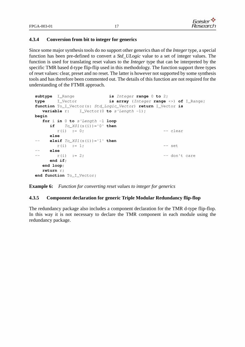
4.3.4 Conversion from bit to integer for generics
Since some major synthesis tools do no support other generics than of the Integer type, a specialfunction has been pre-defined to convert a Std_ULogic value to a set of integer values. Thefunction is used for translating reset values to the Integer type that can be interpreted by thespecific TMR based d-type flip-flip used in this methodology. The function support three typesof reset values: clear, preset and no reset. The latter is however not supported by some synthesistools and has therefore been commented out. The details of this function are not required for theunderstanding of the FTMR approach.
subtype I_Range is Integer range 0 to 2;type I_Vector is array (Integer range <>) of I_Range;function To_I_Vector(s: Std_Logic_Vector) return I_Vector is
variable r: I_Vector(0 to s'Length -1);begin
for i in 0 to s'Length -1 loopif To_X01(s(i))='0' then
r(i) := 0; -- clearelse
-- elsif To_X01(s(i))='1' thenr(i) := 1; -- set
-- else-- r(i) := 2; -- don't care
end if;end loop;return r;
end function To_I_Vector;
Example 6: Function for converting reset values to integer for generics
4.3.5 Component declaration for generic Triple Modular Redundancy flip-flop
The redundancy package also includes a component declaration for the TMR d-type flip-flop.In this way it is not necessary to declare the TMR component in each module using theredundancy package.

FPGA-003-01 18
4.4 Entity of the module
4.4.1 Generic clause
The generic clause contains generics for the redundancy configuration of the modules, as wellas generics for the functionality of the module
4.4.1.1 Redundancy configuration
Each module is configurable for the level and type of redundancy that is to be implemented,featuring the following options:• behavioural or structural implementation:
• behavioural does not allow redundancy, inferred d-type flip-flop insertion is utilised• structural implementation allows redundancy, explicit d-type flip-flop insertion is utilised
• single or redundant sequential element, with• single or triple clocks,• none, single, triple asynchronous reset signals (synchronous reset in combinatorial logic)
• support for combinatorial redundancy, with• no combinatorial redundancy provides single inputs and outputs• combinatorial redundancy provides triplicated input and outputs
• number and type of voters:• no, single or triple input voters before the sequential elements (triple only with
combinatorial redundancy)• no, single or triple output voters after the sequential elements (triple only with
combinatorial redundancy)• logical voters or Xilinx specific tri-state buffer voters
generic(-- Redundancy configurationgStructural: Integer range 0 to 1 := 1; -- behaviour, structuregRedundant: Integer range 0 to 1 := 1; -- no, redundant ffgInVoter: Integer range 0 to 2 := 2; -- 0, 1, or 3 votersgOutVoter: Integer range 0 to 2 := 2; -- 0, 1, or 3 votersgReset: Integer range 0 to 2 := 2; -- sync, async, async*3gClock: Integer range 0 to 1 := 1; -- 1, or 3 linesgCombinatorial: Integer range 0 to 1 := 1; -- no, redundant logicgVoter: Integer range 0 to 1 := 1); -- logical, or tristate
Example 7: Generics for redundancy configuration
4.4.1.2 Functionality configuration
The generics used for configuring the functionality of a module are application dependent anddo not differ from those in other VHDL methodologies. Some restrictions have however beenobserved when combined with this redundancy approach, e.g. it is not always possible to havea generic that controls the width of an array type used for a port. The width of the port will needto be established in the interface package described earlier, since a record cannot haveunconstrained array elements.

FPGA-003-01 19
4.4.2 Port clause
The port clause provides the interface to the module. The ports are split in three groups: clockand reset interface, input interface and output interface.
4.4.2.1 Clock and reset interface
The FTMR approach assumes synchronous design, providing a single clock input that is atriplet. The clock triplet is an array, for which the array elements are numbered 0 to 2. If nocombinatorial redundancy is implemented, only element numbered 0 is used. The holds for thereset triplet. The reset input can be used for synchronous or asynchronous reset. It is possible tobuild a module with more than one clock domain. This requires that both the clock and resetports are separately declared for each clock domain. Transitions between clock domains needto be properly synchronised in the module.
Clk: in Clock_Triple;Rst: in Reset_Triple;
Example 8: Clock and reset interface
4.4.2.2 Input interface
All inputs are defined as triplets. Each input is normally connected to one external module or toa higher hierarchy. Each triplet is an array of a record type, for which the array elements arenumbered 0 to 2. If no combinatorial redundancy is implemented, only the element 0 is used.
---------------------------------------------------------------------------## DEFINE INPUT PORTS AS TRIPLETS-------------------------------------------------------------------------PSRIn: in T_Triple;---------------------------------------------------------------------------## END DEFINE INPUT PORTS AS TRIPLETS-------------------------------------------------------------------------
Example 9: Input interface
4.4.2.3 Output interface
All outputs are defined as triplets. Each output is normally connected to one external module orto a higher hierarchy. Each triplet is an array of a record type, for which the array elements arenumbered 0 to 2. If no combinatorial redundancy is implemented, only the element 0 is used.
---------------------------------------------------------------------------## DEFINE OUTPUT PORTS AS TRIPLETS-------------------------------------------------------------------------PSROut: out T_Triple;---------------------------------------------------------------------------## END DEFINE OUTPUT PORTS AS TRIPLETS-------------------------------------------------------------------------
Example 10: Output interface

FPGA-003-01 20
4.5 Architecture of the module
The architecture of the module is also based on the assumption that the design is synchronous.It is also assumed that there is no mixture between function and interconnectivity within thesame module, although this cannot always be avoided. It is possible to build a module with morethan one clock domain. This requires that the two clock domains are implemented as separateVHDL block statements. Note that this is only one of many possible solutions.
4.5.1 Declarative part
The FTMR approach is based on parts that are pre-defined in a template and parts that need tobe defined by the user for each new module that is being designed. In the declarative part of thearchitecture, the user needs to declare the following items:• private types, constants and subprograms• record of sequential elements• record of combinatorial elements• reset values for sequential elements• explicit conversion from a sequential element record to an array that is used when
instantiating d-type flip-flops• explicit conversion back from an array to a sequential element record• combinatorial behaviour described as a procedure
The main difference between this proposed redundancy approach and normal design is the strictsplit between the different parts listed above, and the additional conversion between records andarrays used for flip-flop instantiation, since this is normally done by inference in synthesis.
4.5.1.1 Definition of private types, constants and subprograms
In this section all private types, constants and subprograms required for describing thefunctional behaviour are defined. Note that these can also be defined in a package.
4.5.1.2 Definition of types for sequential elements
All sequential elements required in the module need to be declared by the user as a single recordtype. The record can be made hierarchical, or nested, for example including the records used forthe output ports as shown in the example below. The record should be constructed not usingtriplet types. Instead, the non-triplicated types and records should be used.
type R_Type is record------------------------------------------------------------------------## DEFINE REGISTERS----------------------------------------------------------------------H: Std_Logic_Vector(7 downto 0); -- randomiser statePSROut: T_Type; -- output------------------------------------------------------------------------## END DEFINE REGISTERS----------------------------------------------------------------------
end record R_Type;
Example 11: Sequential elements (registers)

FPGA-003-01 21
4.5.1.3 Definition of type for combinatorial elements
All purely combinatorial signals required in the module need to be declared by the user as asingle record type. The record can be made hierarchical, or nested, for example including therecords used for the output ports. The record should be constructed not using triplet types,instead the non-triplicated types and records should be used. The difference between thecombinatorial and the sequential elements is that the former do not require any flip-flops orlatches and can be used for describing functionality that is derived combinatorially from flip-flops and inputs. A dummy declaration must always be done when unused.
type C_Type is record------------------------------------------------------------------------## DEFINE COMBINATORIAL SIGNALS----------------------------------------------------------------------Dummy: Std_ULogic; -- unused------------------------------------------------------------------------## END DEFINE COMBINATORIAL SIGNALS----------------------------------------------------------------------
end record C_Type;
Example 12: Combinatorial elements
4.5.1.4 Declaration of reset values
For each sequential element in the module, a reset value should be declared by the user. It ispossible not to declare a reset value for an element, but this is not well supported by thesynthesis tools that have been tried with the methodology. The reset values are declared as partof the Reset function, in which the temporary variable record r is assigned with the reset valuefor each of its elements. A function declaration must always be done even when unused.
function Reset return R_Type isvariable r: R_Type;
begin------------------------------------------------------------------------## DEFINE RESET VALUES FOR REGISTERS----------------------------------------------------------------------r.H := (others => '1');r.PSROut.SyncMark := '0';r.PSROut.FrameMark := '0';r.PSROut.DataMark := '0';r.PSROut.DataStream := '0';------------------------------------------------------------------------## END DEFINE RESET VALUES FOR REGISTERS----------------------------------------------------------------------return r;
end function Reset;
Example 13: Reset function for sequential elements

FPGA-003-01 22
4.5.1.5 Conversion from record to array of bits
The Pack procedure is user-defined and specific to each module. Its purpose is to map the recordtype defining the sequential elements into an array of simple bits. Each array element is latermapped to individual d-type flip-flops. It is not possible simply to map the record type directlyto d-type flip-flops due to limitations in VHDL. Each element in the record r needs to bemapped to an element in the array s. In addition, the variable c is incremented for each element,and returns in the end the number of elements that have been mapped. In some designs it ispreferable that c is calculated directly from the length of the different arrays that can be foundin the record types, using the ‘Length attribute, rather than assuming a fixed length. The cvariable is used for calculating the final length of the array.
In the beginning of a module development, one would normally concentrate on the behaviouralaspect of the design and not apply redundancy. It is therefore possible not to complete the Packand the UnPack procedures when only behavioural implementation is used. A dummydeclaration must however always be done when unused.
procedure Pack(r: in R_Type;
variable s: out Std_Logic_Vector;variable c: inout Natural) is
begin------------------------------------------------------------------------## DEFINE MAPPING----------------------------------------------------------------------c := 0;s(c to c+r.H'Length-1) := r.H;c := c+r.H'Length;s(c) := r.PSROut.SyncMark;c := c+1;s(c) := r.PSROut.FrameMark;c := c+1;s(c) := r.PSROut.DataMark;c := c+1;s(c) := r.PSROut.DataStream;c := c+1;------------------------------------------------------------------------## END DEFINE MAPPING----------------------------------------------------------------------
end procedure Pack;
Example 14: User defined pack function

FPGA-003-01 23
4.5.1.6 Conversion from array of bits to record
The UnPack procedure is user-defined and specific to each module. Its purpose is to map backthe sequential elements from the array of simple bits to the record type. Each element in thearray s needs to be mapped to an element in the record r. In addition, the variable c isincremented for each element, and returns in the end the number of elements that have beenmapped. In some designs it is preferable that c is calculated directly from the length of thedifferent arrays that can be found in the record types, using the ‘Length attribute, rather thanassuming a fixed length. A dummy declaration must always be done when unused.
procedure UnPack(s: in Std_Logic_Vector;
variable r: out R_Type;variable c: inout Natural) is
begin------------------------------------------------------------------------## DEFINE RE-MAPPING----------------------------------------------------------------------c := 0;r.H := s(c to c+r.H'Length-1);c := c+r.H'Length;r.PSROut.SyncMark := s(c);c := c+1;r.PSROut.FrameMark := s(c);c := c+1;r.PSROut.DataMark := s(c);c := c+1;r.PSROut.DataStream := s(c);c := c+1;------------------------------------------------------------------------## END DEFINE RE-MAPPING----------------------------------------------------------------------
end procedure UnPack;
Example 15: User defined unpack function

FPGA-003-01 24
4.5.1.7 Support functions
The following pre-defined support functions provide functionality that is required for mappingthe record type to the array type for the sequential elements. The only thing the user needs to beconcerned with is that for the function R_Length, the array width of the variable s must be largerthan the total number of sequential bits to be implemented. The R_Len constant is used forconstraining the array that carries all sequential elements as individual bits. The simplified Packand UnPack functions are used for direct signal conversion between records and arrays, and viceversa.
function R_Length return Integer isvariable r: R_Type;variable s: Std_Logic_Vector(0 to 1023);variable c: Natural;
beginPack(r, s, c);-- pragma translate_offassert c < s'Length
report "Temporal vector in R_Len function is too short"severity Failure;
-- pragma translate_onreturn c;
end function R_Length;
Example 16: Calculates the width of the array required for all sequential element bits
constant R_Len: Integer := R_Length;
Example 17: The width of the array required for all sequential element bits
function Pack(r: R_Type)
return Std_Logic_Vector isvariable s: Std_Logic_Vector(0 to 1023);variable c: Natural;
beginPack(r, s, c);return s(0 to R_Len-1);
end function Pack;
Example 18: Simplified Pack function
function UnPack(s: Std_Logic_Vector)
return R_Type isvariable r: R_Type;variable c: Natural;
beginUnPack(s, r, c);return r;
end function UnPack;
Example 19: Simplified UnPack function

FPGA-003-01 25
4.5.1.8 Declaration of vector types and signals
The following pre-defined type and signal declarations are used for mapping the record type tothe array type for the sequential elements, and for carrying the outputs of the purelycombinatorial logic. The constant gResetValue is an array of integers, defining the asynchronousreset values for the explicitly instantiated d-type flip-flops. The triplicated signals are used forredundancy purposes. If no redundancy is implemented, as configured with the aforementionedgenerics, only element 0 is used.
type R_Triple is array (Triple) of R_Type;signal R, Rin: R_Triple;
Example 20: Sequential elements as record type
constant gResetValue: I_Vector(0 to R_Len-1) := To_I_Vector(Pack(Reset));
subtype S_Type is Std_Logic_Vector(0 to R_Len-1);type S_Triple is array (Triple) of S_Type;signal S, Sin: S_Triple;
Example 21: Sequential elements as an array of bits
type C_Triple is array (Triple) of C_Type;signal C: C_Triple;
Example 22: Combinatorial logic output as record type
4.5.1.9 Definition of combinatorial behaviour
The combinatorial behaviour of the module is described in the Combinatorial procedure. Thisalso includes the combinatorial logic required for changing the states of the sequential elements.Thus, the only thing that is not described in the procedure is the sequential elements andpotential voters before and after the sequential elements.
procedure Combinatorial(
Example 23: Definition of the procedure for combinatorial logic
4.5.1.9.1 User defined inputs
For a module, all ports that can affect the combinatorial and sequential behaviour are fed to the Combinatorial procedure. This is module dependent. All signals are of the non-triplicated types.
------------------------------------------------------------------------## DEFINE INPUTS----------------------------------------------------------------------signal PSRIn: in T_Type;------------------------------------------------------------------------## END DEFINE INPUTS----------------------------------------------------------------------
Example 24: User defined inputs
FPGA-003-01 26
4.5.1.9.2 Pre-defined input and outputs
The following inputs and outputs to the combinatorial procedure are pre-defined. Rst is the resetinput, R carries the current state of the sequential elements, Rin carries the next state of thesequential elements, and C carries the output of combinatorial logic. All signals are of the non-triplicated types.
signal Rst: in Std_Logic;signal R: in R_Type;signal Rin: out R_Type;signal C: out C_Type) is
Example 25: Pre-defined input and outputs
4.5.1.9.3 Pre-defined variables
The following pre-defined variables are used for temporarily storing the next state of thesequential elements, and the output of the purely combinatorial logic. Rv is used for thesequential elements, and Cv is used for the combinatorial logic. Both variables are of the non-triplicated basic types. All assignments are made to these variables by the user, never to thecorresponding output signals Rin and C. The variables are assigned, as pre-defined in thetemplate, to the corresponding outputs at the end of the procedure, to ensure that there is onlyone such assignment. The user can chose to read the R input or the Rv variable, all dependenton what functionality is required. The R input is unaffected by the assignments in the procedure,whereas Rv can change along the execution of the VHDL code in the procedure description. Rvcan thus be used when the new (or next) combinatorial value is required, rather than the currentvalue of the sequential elements.
variable Rv: R_Type;variable Cv: C_Type;
Example 26: Variable declarations for sequential and combinatorial elements
4.5.1.9.4 Definition of unregistered variables
For temporary variables that do not have a sequential element associated, the variable Uv canbe used. Uv should then be cleared before any usage in the procedure, not to infer any storageelements. A dummy declaration must always be done when unused.
type U_Type is record------------------------------------------------------------------------## DEFINE UNREGISTERED VARIABLES----------------------------------------------------------------------Dummy: Std_ULogic; -- unused------------------------------------------------------------------------## END DEFINE UNREGISTERED VARIABLES----------------------------------------------------------------------
end record U_Type;variable Uv: U_Type;
Example 27: Type and variable declaration for temporary variable

FPGA-003-01 27
4.5.1.9.5 Pre-defined registered variable
At the beginning of the procedure the current state of the sequential elements R is copied to thetemporary variable Rv. This is done to ensure that Rv will not infer any storage elements.
Rv := R;
Example 28: Initialising the Rv variable
4.5.1.9.6 Definition of combinatorial logic
The description of the combinatorial logic is done in a sequence of statements. The Rv variableis to be assigned with the next state of the sequential elements. The Rv variable can also be readin the procedure when an intermediate value is required. Otherwise the R input signal is readwhen the current state of the sequential elements is required. For temporary variables that donot have a sequential element associated, the variable Uv can be used. Uv should then be clearedbefore any usage in the procedure, not to infer any storage elements. No reset statement isrequired in this section, since it is being taken care of later in the procedure for synchronousreset, and in the sequential part for an asynchronous reset.
---------------------------------------------------------------------------## DEFINE COMBINATORIAL LOGIC-------------------------------------------------------------------------if PSRIn.DataMark='1' then -- bit delimiter
if PSRIn.SyncMark='1' then -- sync periodRv.PSROut.DataStream := PSRIn.DataStream; -- uncoded outputRv.H := (others => '1'); -- initialise h(x)
else -- frame or codeblockRv.PSROut.DataStream := -- coded output
PSRIn.DataStream xor R.H(0); Rv.H(7 downto 0) := -- shift h(x)
(R.H(0) xor R.H(3) xor R.H(5) xor R.H(7)) & R.H(7 downto 1); end if;Rv.PSROut.SyncMark := PSRIn.SyncMark; -- delayRv.PSROut.FrameMark := PSRIn.FrameMark; -- delay
elsenull;
end if;Rv.PSROut.DataMark := PSRIn.DataMark; -- delay---------------------------------------------------------------------------## END DEFINE COMBINATORIAL LOGIC-------------------------------------------------------------------------
Example 29: Description of the combinatorial logic

FPGA-003-01 28
4.5.1.9.7 Synchronous reset
The synchronous reset is optional, and is described after the user section mentioned above. Thereset can either be synchronous or asynchronous for the whole module, and is controlled by thegReset generic. It is not possible to have synchronous reset for some sequential elements, andasynchronous reset for other sequential elements in this basic template. If the combinatoriallogic is triplicated, so is the input for the synchronous reset.
if Rst='1' and gReset=0 thenRv := Reset;
end if;
Example 30: Synchronous reset
4.5.1.9.8 pre-defined variables converted to signals
A the end of the procedure, the temporary variable Rv is assigned to the output signal Rin. Theassignment to Rin is made only once not to infer any storage elements. A the end of theprocedure, the temporary variable Cv is assigned to the output signal C. The assignment to C ismade only once not to infer any storage elements.
Rin <= Rv;C <= Cv;
Example 31: Variable to signal assignments
4.5.2 Statement part
The statement part of the architecture instantiates the combinatorial procedure, outputassignments, and sequential elements as inferred or as explicitly instantiated d-type flip-flops.
4.5.2.1 Combinatorial behaviour
The combinatorial behaviour is described by instantiating one or three Combinatorialprocedures. If no combinatorial redundancy is implemented, only instance 0 is used.
CombinatorialGen:for i in 0 to Triple'Right * (gCombinatorial * gStructural) generateCombinatorial(
---------------------------------------------------------------------## DEFINE INPUTS-------------------------------------------------------------------PSRIn => PSRIn(i),---------------------------------------------------------------------## END DEFINE INPUTS-------------------------------------------------------------------Rst => Rst(i),R => R(i),Rin => Rin(i),C => C(i));
end generate CombinatorialGen;
Example 32: Concurrent procedure calls to implement combinatorial logic

FPGA-003-01 29
4.5.2.2 Output ports
All output ports need to be connected to internal sequential elements, R, or to pure combinatoriallogic, C. Each such connection will be instantiated one or three times. If no combinatorialredundancy is implemented, only instance 0 is used. Note the usage of the indices for the R andC signals and the output ports.
OutputGen: for i in 0 to Triple'Right * (gCombinatorial*gStructural) generate
------------------------------------------------------------------------## DEFINE OUTPUTS----------------------------------------------------------------------PSROut(i) <= R(i).PSROut;------------------------------------------------------------------------## END DEFINE OUTPUTS----------------------------------------------------------------------
end generate OutputGen;
Example 33: Output port connection to sequential elements and combinatorial logic
4.5.2.3 Sequential behaviour
The sequential behaviour can either be implemented with inferred or with explicitly instantiatedd-type flip-flops, depending on the use of redundancy.
4.5.2.3.1 Sequential behaviour with explicit flip-flop instances
It is possible to use explicit d-type flip-flop instances without redundancy, this is called thestructural description and is enabled with the gStructural generic. In this case only instance 0is used.
When any kind of redundancy is used, the sequential elements are implemented with explicit d-type flip-flop instances, and the gStructural generic must be enabled. The conversion fromrecord type to array type used for the instantiation of the sequential elements, and vice versa, isperformed in the ConversionGen generate statement.
Note that the reset constant gResetValue is mapped to the rest generic of the d-type flip-flop.The TMR d-type flip-flop implements the triplication of the sequential elements and the voterthat can be placed in front and/or after the flip-flops.
FPGA-003-01 30
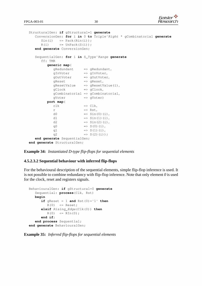
StructuralGen: if gStructural=1 generateConversionGen: for i in 0 to Triple'Right * gCombinatorial generate
Sin(i) <= Pack(Rin(i));R(i) <= UnPack(S(i));
end generate ConversionGen;SequentialGen: for i in S_Type'Range generate
ff: TMRgeneric map(
gRedundant => gRedundant,gInVoter => gInVoter,gOutVoter => gOutVoter,gReset => gReset,gResetValue => gResetValue(i),gClock => gClock,gCombinatorial => gCombinatorial,gVoter => gVoter)
port map(clk => Clk,r => Rst,d0 => Sin(0)(i),d1 => Sin(1)(i),d2 => Sin(2)(i),q0 => S(0)(i),q1 => S(1)(i),q2 => S(2)(i));
end generate SequentialGen;end generate StructuralGen;
Example 34: Instantiated D-type flip-flops for sequential elements
4.5.2.3.2 Sequential behaviour with inferred flip-flops
For the behavioural description of the sequential elements, simple flip-flop inference is used. Itis not possible to combine redundancy with flip-flop inference. Note that only element 0 is usedfor the clock, reset and registers signals.
BehaviouralGen: if gStructural=0 generateSequential: process(Clk, Rst)begin
if gReset = 1 and Rst(0)='1' thenR(0) <= Reset;
elsif Rising_Edge(Clk(0)) thenR(0) <= RIn(0);
end if;end process Sequential;
end generate BehaviouralGen;
Example 35: Inferred flip-flops for sequential elements

FPGA-003-01 31
4.6 Graphical overview of the FTMR approach
A graphical overview of a small design example is shown in figure 10. The design originallyincludes five registers (or flip-flops). The combinatorial logic of the design has been triplicated,as has the inputs and outputs. Some of the outputs stem directly from the flip-flops like in aMoore machine, and some stem from combinatorial logic like in a Mealy machine. All registershave been triplicated inside the TMR blocks, one for each register. There are three voters infront of the triplicated flip-flops, as well as after them. Note the conversion from the record typesignals Rin and R, and the array based signals Sin and S, which is done with the Pack andUnPack functions. All inputs and outputs are based on record type ports. The reset and clockports are also triplicated. The design represent the highest level of redundancy possible with theproposed FTMR approach.
Figure 10: Graphical overview of a design based on five functional registers, providing combinatorial redundancy and sequential redundancy with triplicated input and output voters for the TMR d-type flip-flops.
VVV
V V
V
VVV
V V
V
VVV
V V
V
VVV
V V
V
VVV
V V
V
PACK PACK PACK
Registered
Inputs
UNPACK UNPACK UNPACK Outputs
CombinatorialOutputs
Combinatorial CombinatorialCombinatorial
Clock
Reset
S(0)S(1)
S(2)
Sin(0)Sin(1)
Sin(2)
R(0)R(1)
R(2)
Rin(0) Rin(1) Rin(2)C(0) C(1)C(2)

FPGA-003-01 32
5 RESULTS FROM A SIMPLE APPLICATION
The approach presented in section 3 has been implemented as a VHDL template in which adesigner can describe the desired functionality. The TMR d-type flip-flop has been designedtaking synthesis tool optimisation into account, to avoid the removal of any redundant parts.
A simple pseudo-randomiser design has been developed to demonstrate the effects of thisapproach. The corresponding VHDL source code is provided in its whole in appendix A. Theresults presented in table 1 were obtained after synthesis.
As can be seen from the results above, the triplication of the sequential logic is as predicted. Theincrease of the combinatorial logic varies with the selected level of protection and choice ofvoter approach. The overheads for the combinatorial logic vary from a factor of 3,9 to 11.Predictable, but low performing, results can be best obtained using the Xilinx specific tri-statebuffer voters presented in [RD1].
For a small designs as presented above, all predictions regarding increase in the number of d-type flip-flop and combinatorial resources seem to hold.
All results are based on synthesis using Synplify from Synplicity Inc.
Designseq.
TMR
comb.
TMR
input
voters
output
voters
voter
type
clock
lines
reset
lines
Gate
MHzFFs LUTs
behavioural n/a n/a n/a n/a n/a n/a n/a 224 12 10structural n/a n/a n/a n/a n/a n/a n/a 201 12 13sequential yes no 0 1 logic 1 1 177 36 25sequential yes no 0 1 buffer 1 1 155 36 13sequential - clock yes no 0 1 logic 3 3 177 36 25sequential - clock yes no 0 1 buffer 3 3 155 36 13combinatorial yes yes 1 1 logic 1 1 136 36 63combinatorial yes yes 1 1 buffer 1 1 128 36 39combinatorial yes yes 3 1 logic 1 1 158 36 87combinatorial yes yes 3 1 buffer 1 1 129 36 39combinatorial yes yes 1 3 logic 1 1 136 36 87combinatorial yes yes 1 3 buffer 1 1 129 36 39combinatorial yes yes 0 3 logic 1 1 177 36 75combinatorial yes yes 0 3 buffer 1 1 155 36 39combinatorial - clock & reset yes yes 1 3 logic 3 3 136 36 87combinatorial - clock & reset yes yes 1 3 buffer 3 3 129 36 39combinatorial - clock & reset yes yes 3 3 logic 3 3 158 33 111combinatorial - clock & reset yes yes 3 3 buffer 3 3 129 36 39
Table 1: Synthesis results targeting the Xilinx Virtex XCV1000-6 device

FPGA-003-01 33
6 RESULTS FROM A DEMONSTRATION APPLICATION
A more complex demonstration application was also developed using the proposed mitigationmethod. The application is the CCSDS Time Manager (CTM) [RD8], originally developed atESA. The design was converted using the VHDL template for the proposed redundancyapproach. The development time was about eight hours, including re-running the alreadyavailable test suite which was used for regression testing of the newly developed VHDL code.The synthesis and place & route results of the most interesting configuration cases are presentedin table 2 and table 3.
All synthesis results are based on Synplify from Synplicity Inc. All place & route results arebased on ISE from Xilinx Corporation. Synthesis and place & route has been run using the pushbutton method with default values for most parameters. The target frequency was 40 MHz. Forthe designs implementing combinatorial TMR, the FPGA outputs and inputs have beentriplicated without any additional voting. There was no difference in the synthesis results if thetarget frequency was lowered to 1 MHz.
Design
Configuration Synthesis results Performance
Tim
e (m
in)
seq.
TMR
comb.
TMR
input
voters
output
voters
clock
lines
reset
lines
voter
type FFs
LU
Ts
BU
FGs
BU
FTs Gate
MHz
P&R
MHz
original n/a n/a n/a n/a n/a n/a n/a 786 1457 1 0 42 44 1behavioural n/a n/a n/a n/a n/a n/a n/a 784 1454 1 0 40 46 2structural n/a n/a n/a n/a n/a n/a n/a 784 2015 1 0 38 41 11sequential yes no 0 1 1 1 logic 2352 2793 1 0 37 n/a 24
buffer 2352 2012 1 2352 36 n/a 15combinatorial yes yes 1 1 3 3 logic 2352 7726 3 0 33 n/a 6
buffer 2352 6139 3 4704 33 23 83 3 logic 2352 10861 3 0 34 30 7
buffer 2352 6139 3 >100% 33 n/a 11
Table 2: Synthesis results targeting the Xilinx Virtex XCV1000-6 device
Design
Configuration P & R results
Tim
e (m
in)
seq.
TMR
comb.
TMR
input
voters
output
voters
clock
lines
reset
lines
voter
type FFs
LU
Ts
Slic
es
BU
FTs
GC
LK
s
IOB
s
Gat
es
MH
z
original n/a n/a n/a n/a n/a n/a n/a 785 1438 1072 0 1 122 17686 44 5behavioural n/a n/a n/a n/a n/a n/a n/a 783 1429 1044 0 1 268 17640 46 5structural n/a n/a n/a n/a n/a n/a n/a 783 1998 1049 0 1 268 21354 41 10combinatorial yes yes 1 1 3 3 buffer 2352 6092 5484 4704 3 366 78600 23 126
9% 25% 44% 37% 75% 90% n/a3 3 logic 2352 10751 6540 0 3 366 92475 30 12
9% 43% 53% 0% 75% 90% n/a
Table 3: Place & route results targeting the Xilinx Virtex XCV1000-6 device
FPGA-003-01 34
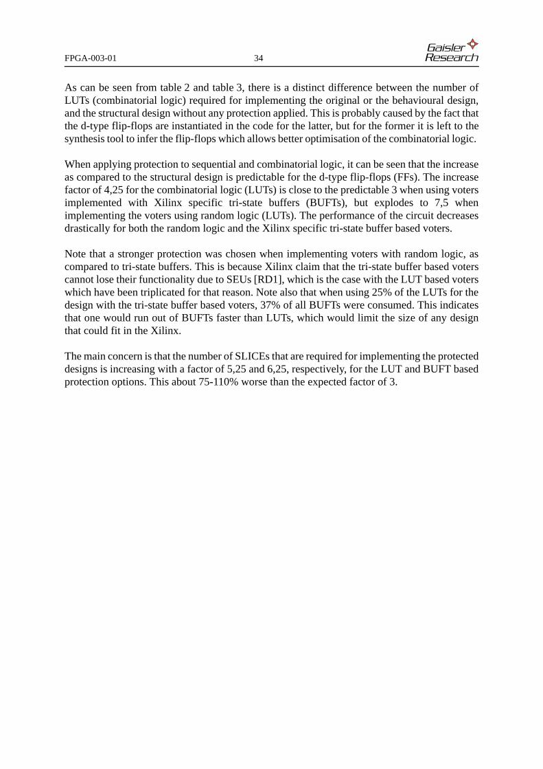
As can be seen from table 2 and table 3, there is a distinct difference between the number ofLUTs (combinatorial logic) required for implementing the original or the behavioural design,and the structural design without any protection applied. This is probably caused by the fact thatthe d-type flip-flops are instantiated in the code for the latter, but for the former it is left to thesynthesis tool to infer the flip-flops which allows better optimisation of the combinatorial logic.
When applying protection to sequential and combinatorial logic, it can be seen that the increaseas compared to the structural design is predictable for the d-type flip-flops (FFs). The increasefactor of 4,25 for the combinatorial logic (LUTs) is close to the predictable 3 when using votersimplemented with Xilinx specific tri-state buffers (BUFTs), but explodes to 7,5 whenimplementing the voters using random logic (LUTs). The performance of the circuit decreasesdrastically for both the random logic and the Xilinx specific tri-state buffer based voters.
Note that a stronger protection was chosen when implementing voters with random logic, ascompared to tri-state buffers. This is because Xilinx claim that the tri-state buffer based voterscannot lose their functionality due to SEUs [RD1], which is the case with the LUT based voterswhich have been triplicated for that reason. Note also that when using 25% of the LUTs for thedesign with the tri-state buffer based voters, 37% of all BUFTs were consumed. This indicatesthat one would run out of BUFTs faster than LUTs, which would limit the size of any designthat could fit in the Xilinx.
The main concern is that the number of SLICEs that are required for implementing the protecteddesigns is increasing with a factor of 5,25 and 6,25, respectively, for the LUT and BUFT basedprotection options. This about 75-110% worse than the expected factor of 3.

FPGA-003-01 35
7 CONCLUSIONS
The presented Functional Triple Modular Redundancy (FTMR) approach to triple modularredundancy for combinatorial and sequential logic on the gate level has shown that it is possibleto write VHDL code in a structured yet high level coding style to obtain the requiredredundancy. The coding approach is template based and only requires a moderate additionaleffort to write as compared to other high level approaches. This structured method also providesbenefits to the source code review process, featuring a clear distinction between sequential andcombinatorial logic. The approach is only applicable to random logic and does not includedprotection for on-chip memories and FPGA interfaces.
The synthesis and place & route results show that the increase of in terms of on-chip resourceusage is higher than expected. The increase for the protection has been observed to be a factorof between 4,5 and 7,5 for the demonstration application. This, together with a performancedecrease of about 50%, could limit the usability of the new protection method.
It is unclear whether the above findings and observed limitations also apply to other types ofgate level mitigation techniques envisaged for Xilinx devices.
Although not a very large design has been produced when writing the document, an assessmenthas been made on whether it is possible to convert the LEON SPARC microprocessor VHDLcode to comply with the proposed FTMR approach. Since LEON is already based on recordtypes for all ports and it already has a clear split between combinatorial and sequential elements,it is considered feasible to do such a conversion.

FPGA-003-01 36
APPENDIX A: VHDL CODE
A.1 TMR D-Type Flip-Flop
--============================================================================---- Design unit : TMR (Entity & architecture declarations)---- File name : tmr.vhd---- Purpose : Triple Modular Redundacy Flip-Flop for the-- Functional Triple Modular Redundacy (FTMR) methodology---- Library : {independent}---- Authors : Mr Sandi Alexander Habinc-- Gaisler Research-- Stora Nygatan 13, SE-411 08 Gteborg, Sweden---- Contact : mailto:[email protected] http://www.gaisler.com---- Copyright (C): Gaisler Research 2002. No part may be reproduced in any form-- without the prior written permission of Gaisler Research.---- Disclaimer : All information is provided “as is”, there is no warranty that-- the information is correct or suitable for any purpose,-- neither implicit nor explicit.---------------------------------------------------------------------------------- Version Author Date Changes---- 0.1 SH 12 Aug 2002 New version-- 0.2 SH 8 Dec 2002 Updated comments--------------------------------------------------------------------------------
library IEEE;use IEEE.Std_Logic_1164.all;
entity TMR is generic(
gRedundant: Integer range 0 to 1 := 1; -- none, or yes gInVoter: Integer range 0 to 2 := 2; -- 0, 1, or 3 voters gOutVoter: Integer range 0 to 2 := 2; -- 0, 1, or 3 voters gReset: Integer range 0 to 2 := 2; -- none, async, async*3 gResetValue: Integer range 0 to 2 := 2; -- clear, set, or none gClock: Integer range 0 to 1 := 1; -- 1, or 3 lines gCombinatorial: Integer range 0 to 1 := 1; -- none, or yes gVoter: Integer range 0 to 1 := 1); -- logical, or tristate port( clk: in Std_Logic_Vector(0 to 2); r: in Std_Logic_Vector(0 to 2); d0: in Std_Logic; d1: in Std_Logic; d2: in Std_Logic; q0: out Std_Logic; q1: out Std_Logic; q2: out Std_Logic);end entity TMR;

FPGA-003-01 37
--============================== Architecture ================================--
architecture RTL of TMR is attribute Syn_Hier: String; attribute Syn_Hier of RTL: architecture is “hard”;
----------------------------------------------------------------------------- -- Local signal declarations ----------------------------------------------------------------------------- -- input data signal i0: Std_Logic_Vector(0 to 2); signal i1: Std_Logic_Vector(0 to 2); signal i2: Std_Logic_Vector(0 to 2); attribute Syn_Keep: Boolean; attribute Syn_Keep of i0: signal is True; attribute Syn_Keep of i1: signal is True; attribute Syn_Keep of i2: signal is True;
-- combinatorial input voter signal v: Std_Logic_Vector(0 to 2);
-- data to flip-flop signal w: Std_Logic_Vector(0 to 2);
-- flip-flop register signal f: Std_Logic_Vector(0 to 2); attribute Syn_Preserve: Boolean; attribute Syn_Preserve of f: signal is True;
-- combinatorial output voter signal f0: Std_Logic_Vector(0 to 2); signal f1: Std_Logic_Vector(0 to 2); signal f2: Std_Logic_Vector(0 to 2); attribute Syn_Keep of f0: signal is True; attribute Syn_Keep of f1: signal is True; attribute Syn_Keep of f2: signal is True; signal o: Std_Logic_Vector(0 to 2);
----------------------------------------------------------------------------- -- Component declarations ----------------------------------------------------------------------------- component TRV is -- Xilinx specific port( -- tri-state voter TR0: in Std_Logic; TR1: in Std_Logic; TR2: in Std_Logic; V: out Std_Logic); end component TRV;
begin -- redundant flip-flops r1: if gRedundant=1 generate -- multiple data inputs k1: if gCombinatorial=1 generate -- multiple combinatorial input voters w2: if gInVoter=2 generate -- copy input to three vectors i0 <= d0 & d1 & d2; i1 <= d0 & d1 & d2; i2 <= d0 & d1 & d2;

FPGA-003-01 38
-- implement one voter for each input copy -- logical voter u0: if gVoter=0 generate v(0) <= (i0(0) and i0(1)) or (i0(0) and i0(2)) or (i0(1) and i0(2));
v(1) <= (i1(0) and i1(1)) or (i1(0) and i1(2)) or (i1(1) and i1(2));
v(2) <= (i2(0) and i2(1)) or (i2(0) and i2(2)) or (i2(1) and i2(2)); end generate;
-- Xilinx tri-state buffer u1: if gVoter=1 generate t0: TRV port map (i0(0), i0(1), i0(2), v(0)); t1: TRV port map (i1(0), i1(1), i1(2), v(1)); t2: TRV port map (i2(0), i2(1), i2(2), v(2)); end generate;
-- concatenate voter results w <= v; end generate; -- single combinatorial input voter w1: if gInVoter=1 generate -- implement a single voter -- logical voter u0: if gVoter=0 generate v(0) <= (d0 and d1) or (d0 and d2) or (d1 and d2); end generate;
-- Xilinx tri-state buffer u1: if gVoter=1 generate t0: TRV port map (d0, d1, d2, v(0)); end generate;
-- copy and concatenate voter result w <= v(0) & v(0) & v(0); end generate; -- no combinatorial input voter w0: if gInVoter=0 generate w <= d0 & d1 & d2; end generate; end generate;
-- single data input, no combinatorial input voter k0: if gCombinatorial=0 generate w <= d0 & d0 & d0; end generate;

FPGA-003-01 39
-- redundant multiple clock line c1: if gClock=1 generate p0: process(clk, r) begin if gReset=2 and r(0)=’1’ then if gResetValue=0 then f(0) <= ‘0’; elsif gResetValue=1 then f(0) <= ‘1’; end if; elsif gReset=1 and r(0)=’1’ then if gResetValue=0 then f(0) <= ‘0’; elsif gResetValue=1 then f(0) <= ‘1’; end if; elsif Rising_Edge(clk(0)) then f(0) <= w(0); end if; end process;
p1: process(clk, r) begin if gReset=2 and gResetValue < 2 and r(1)=’1’ then if gResetValue=0 then f(1) <= ‘0’; elsif gResetValue=1 then f(1) <= ‘1’; end if; elsif gReset=1 and gResetValue < 2 and r(0)=’1’ then if gResetValue=0 then f(1) <= ‘0’; elsif gResetValue=1 then f(1) <= ‘1’; end if; elsif Rising_Edge(clk(1)) then f(1) <= w(1); end if; end process;
p2: process(clk, r) begin if gReset=2 and gResetValue < 2 and r(2)=’1’ then if gResetValue=0 then f(2) <= ‘0’; elsif gResetValue=1 then f(2) <= ‘1’; end if; elsif gReset=1 and gResetValue < 2 and r(0)=’1’ then if gResetValue=0 then f(2) <= ‘0’; elsif gResetValue=1 then f(2) <= ‘1’; end if; elsif Rising_Edge(clk(2)) then f(2) <= w(2); end if; end process; end generate;

FPGA-003-01 40
-- single clock line c0: if gClock=0 generate p0: process(clk, r) begin if gReset=2 and gResetValue < 2 and r(0)=’1’ then if gResetValue=0 then f(0) <= ‘0’; elsif gResetValue=1 then f(0) <= ‘1’; end if; elsif gReset=1 and gResetValue < 2 and r(0)=’1’ then if gResetValue=0 then f(0) <= ‘0’; elsif gResetValue=1 then f(0) <= ‘1’; end if; elsif Rising_Edge(clk(0)) then f(0) <= w(0); end if; end process;
p1: process(clk, r) begin if gReset=2 and gResetValue < 2 and r(1)=’1’ then if gResetValue=0 then f(1) <= ‘0’; elsif gResetValue=1 then f(1) <= ‘1’; end if; elsif gReset=1 and gResetValue < 2 and r(0)=’1’ then if gResetValue=0 then f(1) <= ‘0’; elsif gResetValue=1 then f(1) <= ‘1’; end if; elsif Rising_Edge(clk(0)) then f(1) <= w(1); end if; end process;
p2: process(clk, r) begin if gReset=2 and gResetValue < 2 and r(2)=’1’ then if gResetValue=0 then f(2) <= ‘0’; elsif gResetValue=1 then f(2) <= ‘1’; end if; elsif gReset=1 and gResetValue < 2 and r(0)=’1’ then if gResetValue=0 then f(2) <= ‘0’; elsif gResetValue=1 then f(2) <= ‘1’; end if; elsif Rising_Edge(clk(0)) then f(2) <= w(2); end if; end process; end generate;

FPGA-003-01 41
-- no combinatorial output voter o0: if gOutVoter=0 generate q0 <= f(0); q1 <= f(1); q2 <= f(2); end generate;
-- single combinatorial output voter, one output o10: if (gOutVoter=1 and gCombinatorial=0) or (gOutVoter=2 and gCombinatorial=0) generate
-- logical voter u0: if gVoter=0 generate o(0) <= (f(0) and f(1)) or (f(0) and f(2)) or (f(1) and f(2)); end generate;
-- Xilinx tri-state buffer u1: if gVoter=1 generate t0: TRV port map (f(0), f(1), f(2), o(0)); end generate;
q0 <= To_X01(o(0)); q1 <= ‘-’; q2 <= ‘-’; end generate;
-- single combinatorial output voter, multiple outputs o11: if gOutVoter=1 and gCombinatorial=1 generate -- logical voter u0: if gVoter=0 generate o(0) <= (f(0) and f(1)) or (f(0) and f(2)) or (f(1) and f(2)); end generate;
-- Xilinx tri-state buffer u1: if gVoter=1 generate t0: TRV port map (f(0), f(1), f(2), o(0)); end generate;
q0 <= To_X01(o(0)); q1 <= To_X01(o(0)); q2 <= To_X01(o(0)); end generate;
-- multiple combinatorial output voter o2: if gOutVoter=2 and gCombinatorial=1 generate -- copy input to three vectors f0 <= f; f1 <= f; f2 <= f;

FPGA-003-01 42
-- implement one voter for each input copy -- logical voter u0: if gVoter=0 generate o(0) <= (f0(0) and f0(1)) or (f0(0) and f0(2)) or (f0(1) and f0(2));
o(1) <= (f1(0) and f1(1)) or (f1(0) and f1(2)) or (f1(1) and f1(2));
o(2) <= (f2(0) and f2(1)) or (f2(0) and f2(2)) or (f2(1) and f2(2)); end generate;
-- Xilinx tri-state buffer u1: if gVoter=1 generate t0: TRV port map (f0(0), f0(1), f0(2), o(0)); t1: TRV port map (f1(0), f1(1), f1(2), o(1)); t2: TRV port map (f2(0), f2(1), f2(2), o(2)); end generate;
-- concatenate voter results q0 <= To_X01(o(0)); q1 <= To_X01(o(1)); q2 <= To_X01(o(2)); end generate; end generate;
-- no flip-flop redundancy (no combinatorial redundancy) r0: if gRedundant=0 generate p0: process(clk, r) begin if gReset > 0 and gResetValue < 2 and r(0)=’1’ then if gResetValue=0 then q0 <= ‘0’; elsif gResetValue=1 then q0 <= ‘1’; end if; elsif Rising_Edge(clk(0)) then q0 <= d0; end if; end process; -- unused outputs q1 <= ‘-’; q2 <= ‘-’; end generate;end architecture RTL; -======================================================--

FPGA-003-01 43
A.2 Interface package
--============================================================================---- Design unit : Interface (Package header and body declarations)---- File name : interface.vhd---- Purpose : Interface types---- Library : {independent}---- Authors : Mr Sandi Alexander Habinc-- Gaisler Research-- Stora Nygatan 13, SE-411 08 Gteborg, Sweden---- Contact : mailto:[email protected] http://www.gaisler.com---- Copyright (C): Gaisler Research 2002. No part may be reproduced in any form-- without the prior written permission of Gaisler Research.---- Disclaimer : All information is provided “as is”, there is no warranty that-- the information is correct or suitable for any purpose,-- neither implicit nor explicit.---------------------------------------------------------------------------------- Version Author Date Changes---- 0.1 SH 12 Aug 2002 New version--------------------------------------------------------------------------------
library IEEE;use IEEE.Std_Logic_1164.all;
package Interface is ----------------------------------------------------------------------------- -- Definitions for clock and reset interfaces ----------------------------------------------------------------------------- subtype Reset_Type is Std_Logic; subtype Clock_Type is Std_Logic; subtype Tick_Type is Std_Logic;
----------------------------------------------------------------------------- -- Definitions for input / output interfaces ----------------------------------------------------------------------------- type T_Type is record SyncMark: Std_Logic; -- sync delimiter FrameMark: Std_Logic; -- frame delimiter DataMark: Std_Logic; -- data delimiter DataStream: Std_Logic; -- serial data end record T_Type;end package Interface; --=====================================================--

FPGA-003-01 44
A.3 Redundancy package
--============================================================================---- Design unit : Redundant (Package header and body declarations)---- File name : redundant.vhd---- Purpose : Redundant interface types---- Limitations : Does not support don’t care for asynchronous reset due to-- limitations in Synplify, bug to be reported to Synplicity.---- Library : {independent}---- Authors : Mr Sandi Alexander Habinc-- Gaisler Research-- Stora Nygatan 13, SE-411 08 Gteborg, Sweden---- Contact : mailto:[email protected] http://www.gaisler.com---- Copyright (C): Gaisler Research 2002. No part may be reproduced in any form-- without the prior written permission of Gaisler Research.---- Disclaimer : All information is provided “as is”, there is no warranty that-- the information is correct or suitable for any purpose,-- neither implicit nor explicit.---------------------------------------------------------------------------------- Version Author Date Changes---- 0.1 SH 12 Aug 2002 New version--------------------------------------------------------------------------------library IEEE;use IEEE.Std_Logic_1164.all;
library Work;use Work.Interface.all;
package Redundant is ----------------------------------------------------------------------------- -- Definition of range for Triple Modular Redundancy ----------------------------------------------------------------------------- subtype Triple is Integer range 0 to 2;
----------------------------------------------------------------------------- -- Definitions for clock and reset interfaces ----------------------------------------------------------------------------- subtype Reset_Triple is Std_Logic_Vector(Triple); subtype Clock_Triple is Std_Logic_Vector(Triple); subtype Tick_Triple is Std_Logic_Vector(Triple);
----------------------------------------------------------------------------- -- Definitions for input / output interfaces ----------------------------------------------------------------------------- -- supporting array types for combinatorial redundancy type T_Triple is array (Triple) of T_Type;

FPGA-003-01 45
----------------------------------------------------------------------------- -- Conversion from bit to integer for generics ----------------------------------------------------------------------------- subtype I_Range is Integer range 0 to 2; type I_Vector is array (Integer range <>) of I_Range; function To_I_Vector(s: Std_Logic_Vector) return I_Vector;
----------------------------------------------------------------------------- -- Component declaration for generic Triple Modular Redundancy register ----------------------------------------------------------------------------- component TMR is generic( gRedundant: Integer range 0 to 1 := 1; gInVoter: Integer range 0 to 2 := 2; gOutVoter: Integer range 0 to 2 := 2; gReset: Integer range 0 to 2 := 2; gResetValue: Integer range 0 to 2 := 2; gClock: Integer range 0 to 1 := 1; gCombinatorial: Integer range 0 to 1 := 1; gVoter: Integer range 0 to 1 := 1); port( clk: in Std_Logic_Vector(0 to 2); r: in Std_Logic_Vector(0 to 2); d0: in Std_Logic; d1: in Std_Logic; d2: in Std_Logic; q0: out Std_Logic; q1: out Std_Logic; q2: out Std_Logic); end component TMR;
end package Redundant; --=====================================================--
package body Redundant is ----------------------------------------------------------------------------- -- Conversion from bit to integer for generics ----------------------------------------------------------------------------- function To_I_Vector(s: Std_Logic_Vector) return I_Vector is variable r: I_Vector(0 to s’Length -1); begin for i in 0 to s’Length -1 loop if To_X01(s(i))=’0’ then r(i) := 0; -- clear else-- elsif To_X01(s(i))=’1’ then r(i) := 1; -- set-- else-- r(i) := 2; -- don’t care end if; end loop; return r; end function To_I_Vector;end package body Redundant; --================================================--

FPGA-003-01 46
A.4 Pseudo-Randomiser
--============================================================================---- Design unit : PseudoRandomiser (Entity & architecture declarations)---- File name : psr.vhd---- Purpose : Pseudo-Randomiser---- Library : {independent}---- Authors : Mr Sandi Alexander Habinc-- Gaisler Research-- Stora Nygatan 13, SE-411 08 Gteborg, Sweden---- Contact : mailto:[email protected] http://www.gaisler.com---- Copyright (C): Gaisler Research 2002. No part may be reproduced in any form-- without the prior written permission of Gaisler Research.---- Disclaimer : All information is provided “as is”, there is no warranty that-- the information is correct or suitable for any purpose,-- neither implicit nor explicit.---------------------------------------------------------------------------------- Version Author Date Changes---- 0.1 SH 12 Aug 2002 New version-- 0.2 SH 8 Dec 2002 Updated comments-- 'Length used for Pack/UnPack--------------------------------------------------------------------------------
library Work;use Work.Redundant.all;
entity PseudoRandomiser is generic( -- Redundancy configuration gStructural: Integer range 0 to 1 := 1; -- behaviour, structure gRedundant: Integer range 0 to 1 := 1; -- no, redundant ff gInVoter: Integer range 0 to 2 := 2; -- 0, 1, or 3 voters gOutVoter: Integer range 0 to 2 := 2; -- 0, 1, or 3 voters gReset: Integer range 0 to 2 := 2; -- sync, async, async*3 gClock: Integer range 0 to 1 := 1; -- 1, or 3 lines gCombinatorial: Integer range 0 to 1 := 1; -- no, redundant logic gVoter: Integer range 0 to 1 := 1); -- logical, or tristate port( -- Bit clock and reset interface Clk: in Clock_Triple; Rst: in Reset_Triple;
-------------------------------------------------------------------------- --## DEFINE PORTS AS TRIPLETS -------------------------------------------------------------------------- -- Input interface (bit clock) PSRIn: in T_Triple;
-- Output interface (bit clock) PSROut: out T_Triple); -------------------------------------------------------------------------- --## END DEFINE PORTS AS TRIPLETS --------------------------------------------------------------------------end entity PseudoRandomiser;

FPGA-003-01 47
--============================== Architecture ================================--library IEEE;use IEEE.Std_Logic_1164.all;
library Work;use Work.Interface.all;use Work.Redundant.all;
architecture RTL of PseudoRandomiser is ----------------------------------------------------------------------------- --## DEFINE PRIVATE TYPES, CONSTANTS AND SUBPROGRAMS ----------------------------------------------------------------------------- ----------------------------------------------------------------------------- --## END DEFINE PRIVATE TYPES, CONSTANTS AND SUBPROGRAMS -----------------------------------------------------------------------------
----------------------------------------------------------------------------- -- Type record and array of bits for register file ----------------------------------------------------------------------------- type R_Type is record -------------------------------------------------------------------------- --## DEFINE REGISTERS -------------------------------------------------------------------------- H: Std_Logic_Vector(7 downto 0); -- randomiser state PSROut: T_Type; -------------------------------------------------------------------------- --## END DEFINE REGISTERS -------------------------------------------------------------------------- end record R_Type;
----------------------------------------------------------------------------- -- Type record for combinatorial signals ----------------------------------------------------------------------------- type C_Type is record -------------------------------------------------------------------------- --## DEFINE COMBINATORIAL SIGNALS -------------------------------------------------------------------------- Dummy: Std_ULogic; -- unused -------------------------------------------------------------------------- --## END DEFINE COMBINATORIAL SIGNALS -------------------------------------------------------------------------- end record C_Type;
----------------------------------------------------------------------------- -- Declaration of reset values for register file ----------------------------------------------------------------------------- function Reset return R_type is variable r: R_Type; begin -------------------------------------------------------------------------- --## DEFINE RESET VALUES FOR REGISTERS -------------------------------------------------------------------------- r.H := (others => ‘1’); r.PSROut.SyncMark := ‘0’; r.PSROut.FrameMark := ‘0’; r.PSROut.DataMark := ‘0’; r.PSROut.DataStream := ‘0’; -------------------------------------------------------------------------- --## END DEFINE RESET VALUES FOR REGISTERS -------------------------------------------------------------------------- return r; end function Reset;
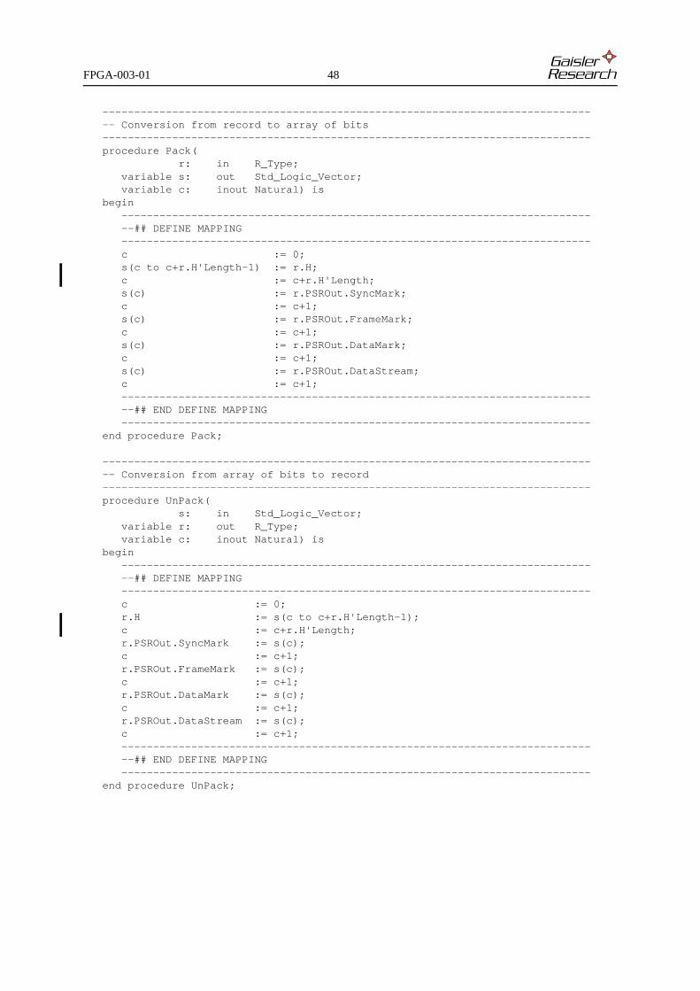
FPGA-003-01 48
----------------------------------------------------------------------------- -- Conversion from record to array of bits ----------------------------------------------------------------------------- procedure Pack( r: in R_Type; variable s: out Std_Logic_Vector; variable c: inout Natural) is begin -------------------------------------------------------------------------- --## DEFINE MAPPING --------------------------------------------------------------------------
c := 0; s(c to c+r.H'Length-1) := r.H; c := c+r.H'Length; s(c) := r.PSROut.SyncMark; c := c+1; s(c) := r.PSROut.FrameMark; c := c+1; s(c) := r.PSROut.DataMark; c := c+1; s(c) := r.PSROut.DataStream; c := c+1; -------------------------------------------------------------------------- --## END DEFINE MAPPING -------------------------------------------------------------------------- end procedure Pack;
----------------------------------------------------------------------------- -- Conversion from array of bits to record ----------------------------------------------------------------------------- procedure UnPack( s: in Std_Logic_Vector; variable r: out R_Type; variable c: inout Natural) is begin -------------------------------------------------------------------------- --## DEFINE MAPPING --------------------------------------------------------------------------
c := 0; r.H := s(c to c+r.H'Length-1); c := c+r.H'Length; r.PSROut.SyncMark := s(c); c := c+1; r.PSROut.FrameMark := s(c); c := c+1; r.PSROut.DataMark := s(c); c := c+1; r.PSROut.DataStream := s(c); c := c+1; -------------------------------------------------------------------------- --## END DEFINE MAPPING -------------------------------------------------------------------------- end procedure UnPack;

FPGA-003-01 49
----------------------------------------------------------------------------- -- Support funcions ----------------------------------------------------------------------------- function R_Length return Integer is variable r: R_Type; variable s: Std_Logic_Vector(0 to 1023); variable c: Natural; begin Pack(r, s, c); -- pragma translate_off assert c < s’Length report “Temporal vector in R_Len function is too short” severity Failure; -- pragma translate_on return c; end function R_Length;
constant R_Len: Integer := R_Length;
function Pack( r: R_Type) return Std_Logic_Vector is variable s: Std_Logic_Vector(0 to 1023); variable c: Natural; begin Pack(r, s, c); return s(0 to R_Len-1); end function Pack;
function UnPack( s: Std_Logic_Vector) return R_Type is variable r: R_Type; variable c: Natural; begin UnPack(s, r, c); return r; end function UnPack;
----------------------------------------------------------------------------- -- Declaration of vector types and signals ----------------------------------------------------------------------------- type R_Triple is array (Triple) of R_Type; signal R, Rin: R_Triple; constant gResetValue: I_Vector(0 to R_Len-1) := To_I_Vector(Pack(Reset));
subtype S_Type is Std_Logic_Vector(0 to R_Len-1); type S_Triple is array (Triple) of S_Type; signal S, Sin: S_Triple;
type C_Triple is array (Triple) of C_Type; signal C: C_Triple;

FPGA-003-01 50
----------------------------------------------------------------------------- -- This defines the combinatorial behaviour. ----------------------------------------------------------------------------- procedure Combinatorial( -------------------------------------------------------------------------- --## DEFINE INPUTS -------------------------------------------------------------------------- signal PSRIn: in T_Type; -------------------------------------------------------------------------- --## END DEFINE INPUTS --------------------------------------------------------------------------
signal Rst: in Std_Logic; signal R: in R_Type; signal Rin: out R_Type; signal C: out C_Type) is variable Rv: R_Type; variable Cv: C_Type;
-------------------------------------------------------------------------- --## DEFINE UNREGISTERED VARIABLES -------------------------------------------------------------------------- type U_Type is record Dummy: Std_ULogic; -- unused end record U_Type; variable Uv: U_Type; -------------------------------------------------------------------------- --## END DEFINE UNREGISTERED VARIABLES --------------------------------------------------------------------------
begin -- pre-defined registered variable Rv := R;
-------------------------------------------------------------------------- --## DEFINE COMBINATORIAL LOGIC -------------------------------------------------------------------------- -------------------------------------------------------------------------- -- This architecture pseudo-randomises the incoming bit stream using the -- following standard polynomial: h(x) = x^8 + x^7 + x^5 + x^3 + 1. -- -- -- +---XOR<----XOR<----XOR<--------------+ input -- | ^ ^ ^ | | -- | | | | | | -- | +-+-+---+-+-+---+-+-+---+---+---+ | v -- +->| 7 | 6 | 5 | 4 | 3 | 2 | 1 | 0 |--+----XOR-> output -- +---+---+---+---+---+---+---+---+ -- -- x^8 x^7 x^6 x^5 x^4 x^3 x^2 x^1 x^0 -- -- (0 xor 3 xor 5 xor 7) & 7654321 => 7 & 6543210 -- -- Many-to-one implementation: Fibonacci version of LFSR -- -- The generator is initialised to all ones durin the ASM period. -- The generated pseudo-random bit stream is xor-ed with the incoming -- bit stream. -- -- Sync and Frame delimiters are delayed one bit clock to match output. --------------------------------------------------------------------------

FPGA-003-01 51
if PSRIn.DataMark=’1’ then -- bit delimiter if PSRIn.SyncMark=’1’ then -- sync period Rv.PSROut.DataStream := PSRIn.DataStream; -- uncoded output Rv.H := (others => ‘1’); -- initialise h(x) else -- frame or codeblock Rv.PSROut.DataStream := PSRIn.DataStream xor R.H(0); -- coded output
Rv.H(7 downto 0) := (R.H(0) xor R.H(3) xor R.H(5) xor R.H(7)) & R.H(7 downto 1); -- shift h(x) end if; Rv.PSROut.SyncMark := PSRIn.SyncMark; -- delay Rv.PSROut.FrameMark := PSRIn.FrameMark; -- delay else null; end if; Rv.PSROut.DataMark := PSRIn.DataMark; -- delay -------------------------------------------------------------------------- --## END DEFINE COMBINATORIAL LOGIC --------------------------------------------------------------------------
-------------------------------------------------------------------------- -- synchronous reset -------------------------------------------------------------------------- if Rst=’1’ and gReset=0 then Rv := Reset; end if; -------------------------------------------------------------------------- -- pre-defined registered variable converted to signal -------------------------------------------------------------------------- Rin <= Rv; -------------------------------------------------------------------------- -- pre-defined combinatorial variable converted to signal -------------------------------------------------------------------------- C <= Cv; end procedure Combinatorial;
begin ----------------------------------------------------------------------------- -- This implements the combinatorial behaviour ----------------------------------------------------------------------------- CombinatorialGen: for i in 0 to Triple’Right * (gCombinatorial * gStructural) generate Combinatorial( ----------------------------------------------------------------------- --## DEFINE INPUTS ----------------------------------------------------------------------- PSRIn => PSRIn(i), ----------------------------------------------------------------------- --## END DEFINE INPUTS ----------------------------------------------------------------------- Rst => Rst(i), R => R(i), Rin => Rin(i), C => C(i)); end generate CombinatorialGen;

FPGA-003-01 52
----------------------------------------------------------------------------- -- Output ports ----------------------------------------------------------------------------- OutputGen: for i in 0 to Triple’Right * (gCombinatorial*gStructural) generate -------------------------------------------------------------------------- --## DEFINE OUTPUTS -------------------------------------------------------------------------- PSROut(i) <= R(i).PSROut; -------------------------------------------------------------------------- --## END DEFINE OUTPUTS -------------------------------------------------------------------------- end generate OutputGen;
----------------------------------------------------------------------------- -- This implements the sequential behaviour ----------------------------------------------------------------------------- StructuralGen: if gStructural=1 generate -------------------------------------------------------------------------- -- Conversion between arrays of records and bits -------------------------------------------------------------------------- ConversionGen: for i in 0 to Triple’Right * gCombinatorial generate Sin(i) <= Pack(Rin(i)); R(i) <= UnPack(S(i)); end generate ConversionGen;
-------------------------------------------------------------------------- -- Sequential behaviour with dedicated flip-flops -------------------------------------------------------------------------- SequentialGen: for i in S_Type’Range generate ff: TMR generic map ( gRedundant => gRedundant, gInVoter => gInVoter, gOutVoter => gOutVoter, gReset => gReset, gResetValue => gResetValue(i), gClock => gClock, gCombinatorial => gCombinatorial, gVoter => gVoter) port map( clk => Clk, r => Rst, d0 => Sin(0)(i), d1 => Sin(1)(i), d2 => Sin(2)(i), q0 => S(0)(i), q1 => S(1)(i), q2 => S(2)(i)); end generate SequentialGen; end generate StructuralGen;

FPGA-003-01 53
BehaviouralGen: if gStructural=0 generate -------------------------------------------------------------------------- -- Sequential behaviour without dedicated flip-flops -------------------------------------------------------------------------- Sequential: process(Clk, Rst) begin if gReset = 1 and Rst(0)=’1’ then R(0) <= Reset; elsif Rising_Edge(Clk(0)) then R(0) <= RIn(0); end if; end process Sequential; end generate BehaviouralGen;end architecture RTL; --======================================================--

FPGA-003-01 54
A.5 Xilinx entities and architectures (not necessary for synthesis)
--============================================================================---- Design unit : BUFT and PULLUP (Entity & architecture declarations)---- File name : xilinx.vhd---- Purpose : Buffer and pullup---- Library : {independent}---- Authors : Xilinx Inc.---- Contact : http://www.xilinx.com---- Copyright (C): Xilinx Inc. 2001.---- Disclaimer : All information is provided “as is”, there is no warranty that-- the information is correct or suitable for any purpose,-- neither implicit nor explicit.---------------------------------------------------------------------------------- Version Author Date Changes---- 1.0 CC 19 Oct 2001 New version--------------------------------------------------------------------------------
library IEEE;use IEEE.Std_Logic_1164.all;
entity BUFT is port( T: in Std_Logic; I: in Std_Logic; O: out Std_Logic);end entity BUFT;
architecture Behavioural of BUFT isbegin O <= To_X01(I) after 5 ns when (T=’0’) else ‘Z’ after 5 ns;end architecture Behavioural;
library IEEE;use IEEE.Std_Logic_1164.all;
entity PULLUP is port( O: out Std_Logic);end entity PULLUP;
architecture Behavioural of PULLUP isbegin O <= ‘H’;end architecture Behavioural;

FPGA-003-01 55
A.6 Xilinx specific triple redundancy voter
--============================================================================---- Design unit : TRV (Entity & architecture declarations)---- File name : trv.vhd---- Purpose : Triple Redundancy Voter---- Library : {independent}---- Authors : Xilinx Inc.---- Contact : http://www.xilinx.com---- Copyright (C): Xilinx Inc. 2001.---- Disclaimer : All information is provided “as is”, there is no warranty that-- the information is correct or suitable for any purpose,-- neither implicit nor explicit.---------------------------------------------------------------------------------- Version Author Date Changes---- 1.0 CC 19 Oct 2001 New version--------------------------------------------------------------------------------
library IEEE;use IEEE.Std_Logic_1164.all;
entity TRV is port ( TR0 : in Std_Logic; TR1 : in Std_Logic; TR2 : in Std_Logic; V : out Std_Logic);end entity TRV;

FPGA-003-01 56 of 56
--============================== Architecture ================================--
architecture RTL of TRV is component BUFT port (I : in std_logic; T : in std_logic; O : out std_logic); end component;
component PULLUP port (O : out std_logic); end component;begin BUFT0: BUFT port map ( I => TR0, T => TR2, O => V);
BUFT1: BUFT port map ( I => TR1, T => TR0, O => V);
BUFT2: BUFT port map ( I => TR2, T => TR1, O => V);
PLLP: PULLUP port map (O => V);
end architecture RTL; --======================================================--
Copyright © 2002 Gaisler Research. Company confidential material and document. This document may notbe distributed under any circumstances. All information is provided as is, there is no warranty that it is corrector suitable for any purpose, neither implicit nor explicit.