fujitsu microelectronics group environmental report … · this brochure is checked with the...
TRANSCRIPT
http://jp.fujitsu.com/fml/en/
Focus on ReadabilityThis brochure is checked with the “Color Selector” software developed by Fujitsu to make the text and images more accessible to a wider range of readers through highly accessible color combinations.
Focus on the EnvironmentThis pamphlet uses paper made from trees harvested from certi� ed forests and is printed with non-VOC ink using a waterless process that does not produce hazardous liquids.
FUJITSU MICROELECTRONICS GROUP
EnvironmentalReport 2009
C 2010 FUJITSU MICROELECTRONICS LIMITED Printed in JapanAD00-00022-2E January, 2010
FUJITSU MICROELECTRONICS LIMITEDEnvironmental Promotion OfficeAkiruno Technology Center, 50 Fuchigami, Akiruno-shi Tokyo 197-0833, JapanTel. +81-42-532-1387http://www.fujitsu.com/global/services/microelectronics/environment/
● For inquiries regarding electronics devices contact:
FUJITSU ELECTRONICS INC.Shin-yokohama Chuo Bldg. 100-45, Shin-yokohama 2-Chome,Kohoku-ku Yokohama Kanagawa 222-8508, Japan +81-120-198-610
Operating hours: 9:00 - 17:00 (except Saturdays, Sundays, national holidays, year-end and New Year holidays)http://jp.fujitsu.com/group/fei/en/
Editorial Policy
The Fujitsu Microelectronics Group Environmental Report 2009 reports the company’s environmental philosophy, its approach and results in conjunction with the electronic devices and semiconductors it handles, based on the Fujitsu Group philosophy and directive, “FUJITSU Way.”We are also reporting on the Fujitsu Microelectronics Group’s activities as understandably as possible on the company website.
Reporting Period
This report covers activities in FY 2008 (from April 1, 2008 to March 31, 2009). However, a portion of the content includes activities both prior to and after April 1, 2009.
Organizations Covered in the Report
All 17 companies in the Fujitsu Microelectronics Group (including overseas companies).
L ifecycle is the Key Concept in Eco-Devices
Our device manufacturing business can impact the environment through greenhouse gases and waste produced by factories, examples of what our device manufacturing business can leave behind as impacts on the environment. To minimize these issues, we are making continual improvements based on the environmental action plan shared throughout the Fujitsu Group. In FY 2008, to curb emissions of gases with high global warming potential, we extended the application of PFC (Per� uorocarbon) gas removal equipment and successfully reduced greenhouse gases other than CO2 emissions by 22% from the preceding year. In addition to making improvements to reduce environmental impact from our group, we also strive to help customers reduce their environment impact, which we consider another important mission for us. In so doing, we � nd it necessary to develop measures such as alleviating the battery dependence of mobile devices that incorporate our products and improving the fuel e� ciency of automobiles. To make this possible, we believe improvements that encompass the entire product lifecycle are essential, including improvement in the manufacturing phase, energy-e� cient design in the design phase, green procurement in the materials procurement phase and reduced packing in the shipping phase. This environmental report includes the improvements Fujitsu Microelectronics Group has made across the whole lifecycle in FY 2008.
Top Message
President
Member of the Board and Corporate Senior Vice President (Environmental Director)
Top Message
Fujitsu Microelectronics Group’s Approach
Reducing Environmental Impact Across the Whole Lifecycle
■The Green Product and Super Green Product Creation
■The Environmental Effi ciency Factor
■Green Procurement
■Approach to Green Distribution
■ Approach to Chemical Substances in Products
■ Representative Green Products
■ Examples of Environmental Contributions through LSI
■Green Factory and Green Offi ce
Global Warming Measures
Chemical and Waste Reduction Measures
Environmental Risk Management
■Environmental Communication
Environmental Social Contribution
External Awards and Environmental Awareness
■Environmental Management System
Environmental Management
FY 2008 Results
Business Activities and Environmental Impact (Material Balance)
Environmental Accounting
See the last page for Fujitsu Microelectronics Group Corporate Profi le
1
2
4
6
7
8
9
13
17
20
22
Appendix
Manufacturing that Contributes to the Global Environment
Approach to the Environment
FUJITSU MICROELECTRONICS GROUP
Environmental Report 2009CON ENTS
O ur Mission is Eco-Device Solutions
Global warming is becoming a serious problem worldwide. A comfortable lifestyle and “realization of a low-carbon society” that protects the global environment are big issues shared by all of society. Fujitsu Group developed its midterm vision, “Green Policy 2020,” based on the pledge at the July 2008 meeting of the G8 (the Hokkaido Toyako Summit) to “halve emissions of greenhouse gases worldwide by 2050.” The Green Policy 2020’s goal is to realize a prosperous, low-carbon society through both internal and societal environmental innovation, centered on the key concepts of creation, collaboration and change. Fujitsu Microelectronics Group, as a member of Fujitsu Group, conducts business based on the guidelines of Green Policy 2020. We believe it is our mission to help our customers enhance their products’ contribution to a low-carbon society through the development and supply of energy-e� cient and compact eco-device solutions. We will continue to pursue device solutions required by the Environmental Age.
● Published: January 2010 (Second edition)● Head of Publishing: President Haruki Okada● Editor in Chief: Hiroshi Osuda, Environmental Promotion O� ce● Issuing Division: Environmental Promotion O� ce, FUJITSU MICROELECTRONICS GROUP● Reference Guidelines: Ministry of the Environment “2007 Environmental Reporting Guidelines”
ECO is in our SEMICONDUCTORs
Working towards a business that delivers device solutions with real value for the needs of the Environmental Age.
FUJITSU MICROELECTRONICS GROUP Environmental Report 2009 | 1

Fujitsu Microelectronics Group’s Approach
Fujitsu Microelectronics Group, based on Fujitsu Group’s shared midterm
environmental vision, Green Policy 2020, aims to realize a prosperous,
low-carbon society by triggering environmental innovation in society
through internal innovation centered on the key concepts of “creation,” “collaboration” and “change.”
We have another goal after the “realization of
a prosperous, low-carbon society.” This is the
realization of our corporate guidelines, the FUJITSU
Way, to “contribute to society and protect the global
environment.”
We strive to be a company that contributes to the
development of a prosperous, low-carbon society
through the pursuit of this midterm environmental
vision, and through this to contribute to the
preservation of the global environment.
Midterm Environmental Vision
Realization of a Prosperous, Low-Carbon Society
Our Final Goal
Contributing to our customers and society
through energy-efficiency, compactness, lightness and
thinness
Inside digital home appliances
Inside mobile devices
Inside automobiles
The EarthContributing to preservation
of the global environment
Fujitsu GroupReducing our own environmental
impact
CustomersReducing our customers'
environmental impact
SocietyIncreasing the environmental
effi ciency of society as a whole
The Earth
By reducing our customers' and society's
environmental impact, we contribute to the
preservation of the global environment.
Inside offi ce equipment
With our customers, we contribute to the protection of a rich global environment, using state-of-the-art technology to provide
semiconductor devices with superior environmental characteristics.
By applying the following principles, we work to prevent pollution of the globalenvironment and reduce the environmental burden of our products throughout their life-cycles,
including development, procurement, manufacture, sales, usage, and disposal:
Through aggressive promotion of Super Green Product development, we improve the environmental characteristics of our products and actively contribute to reducing the burden on the global environment and our customers.
We aggressively promote measures to counteract global warming and reduceemissions of greenhouse gases (e.g. CO2, PFCs).
We aggressively promote chemical management and reduced emissions of volatileorganic compounds (VOCs).
We aggressively promote waste reduction and appropriate recycling.
We conform to environmental regulations around the world and keep our promisesto customers.
We work to improve the individual environmental consciousness of each of ouremployees, to help them become good environmental citizens.
We expand the e� ectiveness and transparency of our environmental managementsystem, driving continuous improvement and development.
OperationPrinciples
1
2
3
4
5
6
7
Fujitsu Microelectronics Limited
Environmental Policy
2 | FUJITSU MICROELECTRONICS GROUP Environmental Report 2009 FUJITSU MICROELECTRONICS GROUP Environmental Report 2009 | 3

Reducing Environmental Impact Across the Whole Lifecycle
Reducing Environmental Impact Across the Whole Lifecycle
From development and design to manufacture and usage –Constructing a business process with low environmental impact across the whole lifecycle of the semiconductor product
Development and design Manufacturing (back-end)Material procurement Distribution and salesManufacturing (front-end) Usage
● Low-power ICs・ Multiple power source design technology
that reduces power consumption while active
・ Power-gating design technology that reduces power consumption when idle・ “RDF V4.0,” a development system loaded
with the features of a multiple power source design and power-gating design
● Green processes・ Massive time-saving and
productivity increases・ Coordination with production innovation
project (Toyota production system)
● Green factories・Reducing greenhouse gas emissions・Reducing waste emissions・ Reducing emissions of VOC (volatile
organic compounds)
● Green procurement・ Working with our partners to promote
green procurement, under the Fujitsu Group's green procurement standards・ Supporting our partners' construction
of CMS (central management systems) based on the JGPSSI*1 "Guidelines for the Management of Chemical Substances in Products"
● Green distribution
・ Shipping with low CO2 emissions
・Terminals installed on vehicles to improve fuel e� ciency
● Packing・Usage of specialized reusable boxes・ Application of cobalt-chloride-free
humidity indicators
● Green processes・ Process improvement reducing the
amount of chemicals and gas used・Reduction of process energy expenditure・ Clari� cation of improvement priorities
using the CG index*2
● Green factories・Saving energy to reduce CO2 emissions・ Changing from PFC gas*3 to gases of low
global warming potential, and installing manufacturing lines equipped with PFC gas harm removal equipment
・Curtailing sludge waste emissions with the introduction of a "Fluorine Recovery and Reuse System"
・ Reducing emissions of VOC (volatile organic compounds)
● Green products and Super Green Products・Products adapted to our special
environmental awareness standards・Products with improved environmental
e� ciency・Environmental improvement solutions
using ICs of superior environmental performance
*1 JGPSSI: Japan Green Procurement Survey Standardization Initiative
*2 Cost Green index. Fujitsu Group's unique index calculated by multiplying the following three factors: material input per unit of product, unit value, and degree of environmental impact.
*3 Per� uorocarbon gas. Used in the manufacturing of semiconductors; it has a global-warming potential approximately 10,000 times higher than that of CO2.
Business Facilities
Development and design bases Manufacturing bases
● FUJITSU MICROELECTRONICS LTD. (Headquarters/Akiruno Technology Center)● FUJITSU ELECTRONICS INC.● FUJITSU VLSI LTD.● FUJITSU LSI TECHNOLOGY LTD.● FUJITSU LSI SOLUTIONS LTD.● FUJITSU MICROELECTRONICS SOLUTIONS LTD.● FUJITSU MICROELECTRONICS AMERICA, INC. ● FUJITSU MICROELECTRONICS EUROPE GmbH ● FUJITSU MICROELECTRONICS ASIA PTE. LTD. ● FUJITSU MICROELECTRONICS PACIFIC ASIA LTD.● FUJITSU MICROELECTRONICS (SHANGHAI) CO., LTD. ● FUJITSU MICROELECTRONICS KOREA LTD. ● FUJITSU GLOBAL MOBILE PLATFORM INC.
● FUJITSU MICROELECTRONICS LTD. (Mie Plant/Aizuwakamatsu Plant/Iwate Plant)
● FUJITSU SEMICONDUCTOR TECHNOLOGY, INC.
● e-Shuttle, Inc.
● FUJITSU INTEGRATED MICROTECHNOLOGY LTD. (Aizu Plant/Miyagi Plant/Kyushu Plant)
● FUJITSU FACILITIES ENGINEERING LTD.
4 | FUJITSU MICROELECTRONICS GROUP Environmental Report 2009 FUJITSU MICROELECTRONICS GROUP Environmental Report 2009 | 5

Manufacturing that Contributes to the Global Environment
When developing new LSIs, Fujitsu Microelectronics Group aims to reduce the environmental impact of the customer product that incorporates the LSI, and to reduce the environment impact of the � nal use of the product, thereby reducing the environmental impact on all of society. To realize these goals, Fujitsu Microelectronics Group utilizes the framework of “Green Product and Super Green Product Creation” to create eco-friendly products.
Green Product and Super Green Product Evaluation Framework
All products undergo a “Green Product Assessment” before development to evaluate factors such as energy e� ciency and chemical suitability. After making design improvements to bring the assessment score to 90 or higher, development begins. After development, a follow-up evaluation is conducted to verify that the original goals have been achieved. LSIs with energy e� ciency, 3R score and chemical suitability, etc. that are superior to other products on the market other Fujitsu Microelectronic Group products are certi� ed as “Super Green Products” and actively promoted to customers.
To provide environmentally e� cient products and services to our customers, we promote green procurement in the materials procurement and outsourced services involved in product development and design, manufacturing, distribution and sales while receiving assistance from our business partners.
Enhanced Environmental Activities in the Supply Chain
Through the procurement of outsourcing services involved in product development, design and manufacturing, our environmental activities aim at:
・ The promotion of an improved EMS (Environmental Management System) at our business partners.・ The promotion of the building of a CMS (Chemical Substances Management
System)
Our goal is to achieve and maintain 100% procurement from business partners with complete EMS and 100% CMS completion as our materials providers. EMS-complete business partners have a Level 1 or higher EMS rating (for material providers, Level 2 or higher is required), and CMS-complete business partners have received a CMS audit by Fujitsu Microelectronics Group and have a rating of Level B or higher. Furthermore, for business partners that are not shared with Fujitsu, we conduct an EMS level survey, request and encourage them to pursue a higher level of accreditation, and promote the signing of a “Green Procurement Agreement” demonstrating the completion of CMS.
In FY 2007, Fujitsu Group introduced the “Environmental E� ciency Factor” as an index to gauge the environmental performance of its products, which Fujitsu Microelectronics subsequently adopted for implementation.
Environmental E� ciency Factor Methodology
The Environmental E� ciency Factor is calculated with the ratio of “product value” divided by the “environmental impact.”
Green Procurement
The Environmental Effi ciency Factor
Super Green Products (Top environmental products)
Green Products(Highly environmentally-conscious products)
Step1
where all evaluation criteriahave been met
where overall score is90 points or higher
Step2Implementation of
“Green Product Evaluation”
Implementation of “GreenProduct Assessment”
where environmental factors correspond with
“Super Green Product de� nition”
Step3
Evaluation of environmental factors based on the definition of
“Super Green Product”
The Green Product and Super Green Product Creation
FUJITSU MICROELECTRONICS LTD.Business Planning & Promotion Div.
Chisa Ubagai (Left)Chie Yamazaki (Right)
We handle the EMS environmental survey and signing of CMS “Green Procurement Agreements.” We are engaged in environmental activities including the CMS management of partner manufacturers that directly use regulated materials and the EMS management of all business partners including non-manufacturers. We plan to continue to support the activities of our business partners and to enhance the Green Procurement activities of Fujitsu Microelectronics Group.
VOICE
● Results of FY 2008 Activities
EMS-complete business partners CMS-complete business partners
Level 1: 13 30% Level A: 15 100%
Level 2: 3 7% Level B: 0 ─
Level 3: 27 63% Level C: 0 ─
Levels 1-3 total Levels A-C: 43 100% 15 100%
VOICE
FUJITSU MICROELECTRONICSSOLUTIONS LTD.SoC Technology Dept. Development Div.ⅠTakayoshi Kyono
Our environmental philosophy is to “refi ne our technology and contribute to the global environment and society.” To reduce our environmental impact, our team is applying low-energy methods to our LSI development ahead of competitors and pursuing technology for even further energy savings.
FUJITSU ELECTRONICS INC.Eastern Japan Sales Div.Ⅲ
Tatsuya Yoshida
How Sales Workforce Can Contribute to the EnvironmentOur clients who develop mobile devices have a strong demand for low power consumption. The change to low power consumption not only contributes to the environment, but also allows the package to be more compact and extends continuous usage time. In sales, we work daily to contribute to the environment and consumer products by offering and having low-power products adopted. As an individual, I use a multi-outlet extension cord with a switch to reduce the required standby electricity.
Environmental e� ciency factor
Product performance and function, including basic design, etc.
Power consumption, etc.
Product value(New vs. old product)
EnvironmentalImpact
(New vs. old product)
=Higher value
Lower environmentalimpact
VOICE
6 | FUJITSU MICROELECTRONICS GROUP Environmental Report 2009 FUJITSU MICROELECTRONICS GROUP Environmental Report 2009 | 7

Manufacturing that Contributes to the Global Environment
Representative Green Products
We consider the environment even in the distribution of our products. Semiconductors are packed and shipped in square-shaped trays or rolled onto tubes in tape-shaped containers. We are environmentally conscious about our shipping materials, reusing these trays and using plant-based resins in our tape. We also use specialized containers to reduce the use of cardboard boxes in our packaging.
Increase Rate of Tray Reuse
To increase our rate of tray reuse, we strive to collect shipped trays with the cooperation of a collection company. We also strive to increase their strength so the trays may be used over a long period of time. In 2008, we achieved a reuse rate of 50%.
Approach to Green Distribution
A cargo container
Meeting on chemical substance handling
● Packing materials and reducing CO2 in distribution
During shipping from our semiconductor factories to our distribution centers, we use reusable cargo containers instead of cardboard boxes. As a result of this reduction in cardboard box use and improvement of our loading ratio, we have been able to reduce CO2 in distribution.
Approach to Chemical Substances in Products
In addition to strictly following legal bans and regulations on chemical substances, Fujitsu Microelectronics Group takes a “precautionary principle” approach to manufacture and providesproducts free of harmful chemical substances by maintaining policies for handling chemical substances that may be hazardous.
As a member of the Fujitsu Group, Fujitsu Microelectronics Group de� nes legally regulated substances as “Fujitsu Group Designated Prohibited Substances” and only provides products that do not contain prohibited substances. We also de� ne substances that may be harmful as “Fujitsu Group Designated Controlled Substances” and control the amount of their inclusion.
Approach to legal regulations
In the divisions assuming product-related responsibilities such as the products, quality assurance, purchasing and environmental divisions, a CMS*1 has been put in place to ensure thorough chemical substances management in each process from design to shipping, working daily to provide products that are compliant with various regulations including Europe’s RoHS*2, China’s RoHS*3 and REACH*4. In the semiconductor manufacturing process, we do use chemicals containing PFOS*5, which can have negative e� ects on ecosystems. Their controlled use in semiconductors is deemed acceptable in international and domestic regulations such as the POPs treaty*6 and the Act on the Evaluation of Chemical Substances and Regulation of Their Manufacture.*7 The Fujitsu Microelectronics Group thoroughly manages the use of chemicals containing PFOS while seeking a transition to safer chemicals.
*1: CMS: chemical substances management
*2: European RoHS Directive (EU regulations): A set of directives restricting the use of speci� ed Harmful Substances contained in electric and electronic devices
*3: China RoHS (Chinese regulations): Administration on the Control of Pollution Caused by Electronic Information Products
*4: REACH: A regulation regarding the Registration, Evaluation, Authorisation, and Restriction of Chemicals
*5: PFOS: Per-� uorooctane sulfonate
*6: POPs treaty (international treaty): Stockholm Convention on persistent organic pollutants (POPs)
*7: Act on the Evaluation of Chemical Substances and Regulation of Their Manufacture, etc.: Japanese regulatory act
Product Category Microcontrollers
DC Brushless Motor Control MCUModel: MB91490 series
■ Product OverviewThe MB91490 series maintains the CPU function of the MB91470/480 series microcontrollers used for high-performance motor control while achieving fewer pin counts and smaller packages. Speci� cations have been optimized from previous products to reduce power consumption. With the newly added low-voltage detection interrupt/reset function, the product is fail-safe compatible.
■ Application: Industrial uses, and air-conditioner and washer-dryer motors
Environmental Characteristics
❶ Part mounting area reduced by approximately 66mm2*1
❷ Power consumption reduced by approximately 15%*2
*1: Corresponds to two low-voltage detection devices
*2: Compared with former Fujitsu Microelectronics Group products
1FUJITSU MICROELECTRONICS LTD.Standard MCU Design Dept.Security & Ecology Business Div.
Koji Takenouchi
The installation of various fail-safe functions*3 is becoming the industry standard in the white home appliance these days. One of these fail-safe functions is low-voltage detection interrupt/reset. Previously low-voltage detection devices and the microcontroller needed to be installed individually. But with the MB91490 series, the function is included in the microcontroller, reducing the number of parts and the footprint of the board. The MB91490 series is positioned as a less-pin version of the MB91470/480 series while maintaining the same 80MHz CPU function, meaning small installation area and the fast, real-time information processing compared to prior products. I hope to continue to develop microcontrollers that are both eco-friendly and valuable when incorporated into customers’ products and systems.
*3: Function that ensures constant safe functioning when the system or devices undergo interruptions due to incorrect operation or malfunctions.
VOICE
Environmental Characteristics
❶ Conversion e� ciency: 96% (input: 12V, output: 5V)❷ Current consumption: Reduced by 55%*1
❸ Reduced board area/reduced number of parts: Use of the “bottom detection comparator system” makes
the phase compensation circuit unnecessary. Also includes a bootstrap diode.
*1: Compared with previous Fujitsu Microelectronics Group products
Product Category Analog
Universal DC/DC Converter ICModel: MB39A138
■ Product OverviewTwo-channel power IC for digital consumer electronics that allows safe, high-speed operations even during rapid high-current load changes. Used in double-speed and full-HD big-screen television and fast image-processing, high-performance video game consoles.
■ Application: Digital televisions, Blu-ray recorders, DVD recorders, television converters, video game consoles, projectors, copy machines
2FUJITSU MICROELECTRONICS LTD. Analog Products Marketing & Application Eng. Dept. Security & Ecology Business Div.Shu Yi
Our “bottom detection comparator system” constantly compares the feedback voltage from the output and the reference voltage by a high-speed comparator, maintaining a fi xed output voltage by fi xing the ON period and controlling the OFF period. As a result, during output voltage changes resulting from rapid load changes, the operating frequency is immediately adjusted to ensure constant stabilization of the output voltage frequency. Use of this system results in superior power conversion effi ciency and voltage stability compared to previous voltage/current control systems. As a result, the system is supplied with stable current, and the number of smoothing output capacitors is greatly reduced, contributing to overall parts cost reduction for the set.
VOICE
8 | FUJITSU MICROELECTRONICS GROUP Environmental Report 2009 FUJITSU MICROELECTRONICS GROUP Environmental Report 2009 | 9

Manufacturing that Contributes to the Global Environment
Product Category ASSP (Security)
Ultra-High-Speed Security ProcessorsModel: MB86C61/60A
■ Product OverviewThe MB86C61/60A is a security processor that connects with Ethernet and conducts encryption processing. Through architecture optimized for packet processing, we achieved duplex 1Gbps full-wire IPsec processing at the low operating frequency of 150MHz with reduced power consumption of approximately 600mW.
■ Application: Network equipment
Environmental Characteristics
❶ Reduced energy consumption from 6W to 600mW*1
Energy consumption reduced by 90% through low operating frequency processing
*1: When processing the same performance with software
5FUJITSU LSI SOLUTION LTD.Broadband Security Development Dept.
Norio Abe
The ultra-high-speed security processor MB86C61/60A that we have developed provides the rapidly enlarging IP network security with both high performance and low energy consumption. Our day-to-day work in the environment and security has been highly praised, winning 2nd Place in the 2009 “Semiconductor of the Year” contest. We hope to continue to provide products that contribute to “building a comfortable and safe network society.”
VOICE
Product Category ASSP
1394 Automotive Controller IC Model: MB88395
■ Product OverviewMakes wide-area transmissions possible through conversion of the physical layer to 800Mbs and an increased compression rate for SmartCODEC, allowing multiple signals (including Blu-ray disk, digital television, HD video, as well as highly detailed displays of vehicle navigation), to be transmitted simultaneously on a single network without a sense of delay.
■ Application: Car entertainment systems such as Blu-ray and car navigation systems
Environmental Characteristics
❶ Reduced energy consumption by 46%*1 930mW to 500mW❷ Part mounting area reduced by 62%*1 676mm2 to 256mm2
❸ Compatible with Ultra Low Power Mode Standby current of below 40µA
*1: Compared with previous MB88388A
4FUJITSU MICROELECTRONICS LTD.Solution Engineering Dept.Automotive Business Div.
Hideo Makabe
In converting to an FBGA package to reduce the part mounting area, problems with increasing thermal resistance were encountered. To guarantee proper operation at 95ºC, the issue became how to reduce the energy consumption suffi ciently. By using the 90nm process to reduce internal logic voltage, reducing the speed of the SmartCODEC operation clock and reducing the energy consumption of the analog circuits, we were able to reduce energy consumption compared with previous products by 46%. Use of this product can reduce the overall number of system parts and the number of wire harnesses, can improve mileage through the lightening of the vehicle and can reduce CO2, contributing to the environment.
VOICE
FUJITSU MICROELECTRONICS LTD.Graphics and Imaging Dept.Automotive Business Div.
Kouwa Shibata
The issue was how to achieve a powerful video input/output function and high-end image processing IC in a single chip. What’s more, it needed to fi t in the same size package as before and to guarantee function at temperatures of 85ºC when used in automobiles. In the course of development, we decided to stop each and every one of the clocks on individual modules when not in use, reduced energy consumption, employed a new package to improve the thermal resistance, conducted heat analysis while simulating as closely as possible the conditions of use by the customer, and fi t the LSIs into the same package as used previously. Use of this product can reduce the total number of system parts, achieve improved mileage by lightening the system, and support eco-drive through the display of mileage and driving conditions.
VOICE
Product Category ASSP (Automobiles)
Automobile Graphics Display ControllerModel: MB86298
■ Product OverviewIndustry-leading drawing function and OpenGL ES2.0 compatible graphics function support the even higher quality display of three-dimensional vehicle navigation. Also, through four display outputs and four video inputs, images from multiple cameras around the vehicle can be composed and converted in real time to be displayed as one image on the dashboard.
■ Application: Digital dashboard and vehicle navigation systems
Environmental Characteristics
❶ Multiple image input/output function possible on one chip, contributing to reduced number of parts of PCBs*1.
❷ Support for suspend mode*2 (when in suspend mode, energy consumption can be reduced by 500mW)
*1: Print circuit board
*2: Only DDR2 IF
3
Product Category ASSP (imaging)
H.264/MPEG-2 Full HD Transcoder LSAModel: MB86H57/58
■ Product OverviewProduct that converts full-HD (1920 dots x 1080 lines) MPEG-2 format and H.264 format video and sound data. Through proprietary transcoding technology, we have achieved industry-leading low power consumption of 1.0W during transcoding including the power consumption of in-package memory.
■ Application: Digital recording equipment
Environmental Characteristics
❶ Energy consumption reduced by 65%*1 (approximately 1.7W) through proprietary transcoding technology and SiP with FCRAM
❷ Function required for recording of digital broadcasts included in one chip, with mounting area reduced by 75%*2 through the use of compact packages.
6
FUJITSU MICROELECTRONICS LTD.Digital Imaging Design Dept.Infotainment Solution Div.
Toshio Hosoi
This product converts between the MPEG-2 format and H.264 format video and sound data for electronic equipment with digital broadcast recording functions such as hard disk recorders and personal computers. Power consumption increased during high-speed processing of large amounts of video and sound data in previous products, including those of our competitors, and the need for large amounts of external memory were also issues. The product we have developed this time provides high image quality and low energy consumption simultaneously through the use of our proprietary transcoding technology. It also utilizes the 65nm process and our fi rm’s high-speed, low-energy memory FCRAM installed as SiP, realizing further reduced energy consumption and compactness. As a result, this product can be installed in mobile devices such as personal computers.
VOICE
*1: Compared with previous Fujitsu Microelectronics Group products
*2: For H57. Compared with previous Fujitsu Microelectronics Group products
10 | FUJITSU MICROELECTRONICS GROUP Environmental Report 2009 FUJITSU MICROELECTRONICS GROUP Environmental Report 2009 | 11

down up
Power
Time
Active
Standby
Ave.
Active
Manufacturing that Contributes to the Global Environment
Product Category Memory
Consumer FCRAMModel: MB81EDS516545
■ Product OverviewThis low-power memory is for digital consumer electronics using a 512M-bit, low-
power DDR interface. With this product, we have realized SiP solutions by memory
which previously had temperature-range constraints through the ability to operate
at 125ºC. We also reduced energy use by 50% compared to two DDR2 SDRAMs.
■ Application: Digital consumer electronics
Environmental Characteristics
❶ Energy reduction of around 54%*1
Yearly CO2 emission reduction of 14.6K tons*2 possible
❷ Printed circuit board mounting area reduced 22% through conversion to SiP*3
*1: Compared to two DDR2 SDRAMs
*2: Based on 20% of LCD televisions shipped worldwide in 2009 using FCRAM
*3: Compared to two LCD television DDR memory locations converted to SiP
8FUJITSU MICROELECTRONICS LTD.FCRAM Design & Characterization Dept.Infotainment Solution Div.
Daisuke Kitayama
With this product, we were the fi rst in the industry to realize the 125°C operation in memory with a DDR interface. In development, we struggled with the fact that the unique variation became more pronounced as the temperature range widened, requiring very precise design. Furthermore, since we had no experience in developing memory chips with the 125°C operation, a complete review of the environment and methods for testing, property evaluation and reliability evaluation was required. The fact that we solved these technological challenges and were able to meet the development schedule was very encouraging for the entire team. We believe products with superior features such as low power consumption contribute to the environment. We plan to continue to develop FCRAM products that benefi t both the end product for the customer and the environment.
VOICE
Fujitsu Microelectronics Group provides optimal low-power LSIs and high-performance, varied device solutions that achieve compact, lightweight products for the customer through the combination of high-performance, environmentally focused design technology.
Examples of Environmental Contributions through LSI
Applying the low-power design flow RDF4.0 to microcontrollers
As the demand for further low-power consumption in LSIs becomes more and more intense, the leak current of the transistor while the device is idle is increasing, a result of resulting from the miniaturization process. In products where battery life is an issue such as mobile devices, this problem cannot be ignored. Fujitsu Microelectronics Group uses low-power design � ow RDF4.0 to signi� cantly reduce standby current in our microcontroller products.
We have dramatically facilitated the logic and physical design of multiple power supply design and power gating by supporting the industry-standard power supply description format, "CPF" ahead of others in the industry. Also, in our power-gating technology, we have developed a proprietary power-supply switch control circuit and switch-parameter-adjustment method to reduce noise generated when the power supply shuto� switch is on. Through this technology, power-gating products can be operated more stably. This technology also applies to microcontroller design, making reduced low power consumption and reduced power consumption especially during standby achievable without large delays in the design period.*1
*1: The most di� cult evaluation processes are reduced to around 1/10th the time.
Example1
FUJITSU MICROELECTRONICS LTD.Design Innovation Engineering Dept.ENVM Technology Development & Products Engineering Div.Tsutomu Nakamori
With this successful application of the low-power consumption Flow RDF 4.0 technology to microcontroller design, we are proud of the fact that we have contributed to making customer products low power, reducing CO2 emissions and improving the environment a little.
VOICE
Multiple power supply speci� cationLibrary selection
DFT*3 by power domain
Voltage consideration and synthesis
Multiple power supply sourcesPower veri� cation
Power supply gating insertionLevel shifter/isolator insertionOptimization
Sign-o� veri� cationMulti-Vdd sign o� veri� cationLVS veri� cation
LSI speci� cation
Test synthesis
Logic synthesis
RTL*1 design power supply domain de� nition
Layout
Veri� cation
CPF*2
Environmental Characteristics
❶ Operating power reduced by 36%*1
(part mounting area reduced by 60%)
❷ Energy-saving mode equipped. Reduced to 0.5mA*2 during
intermittent operation with chipset level.
*1: Compared with previous products (MB86K21)
*2: In energy-saving mode when combining our � rm’s RF-LSI and power LSI
Product Category ASSP (communications)
Mobile WiMAX Baseband LSIsModel: MB86K23
■ Product OverviewWe developed a Mobile WiMAX baseband LSI targeting mobile devices, the market for which is expected to grow. Through the combination of our � rm’s RF LSI (MB86K52) and power LSIs, we have achieved a compact mobile WiMAX terminal and extended operation.
■ Application: Mobile WiMAX communication devices
7FUJITSU MICROELECTRONICS LTD.WiMAX SoC Design Dept.Mobile Solution Div.
Motohisa Ikeda
In battery-driven mobile devices, low-power design in intermittent operation (the autonomous repeating of communication activity and static activity), a challenge unique to this fi eld, was an important issue. This product uses low-power technology including 65nm generation CMOS low-energy process technology and power gating in the baseband LSIs. It also combines our fi rm’s RF-LSI and power LSI. By optimizing design through baseband internal processor software that includes energy-reduction control, we have achieved a low-energy chipset. We plan to continue to pursue energy-reducing technology in both hardware and software and to contribute to the extended use of mobile devices.
VOICE
*1: RTL (register transfer level): process to convert user speci� cations into register transfer level notation
*2: CPF (common power format): common format to notate circuit speci� cations and restricting conditions in circuits used to achieve lower power consumption such as control circuits for leaked current.
*3: DFT (design for test): method of including structures to identify defects in semiconductor circuit design in the manufacturing phase
Around a 54%
reduction
27.2
12.65
Using SDRAM Using FCRAM
10
15
20
25
30
CO2 Em
issions(thousands of tons)
12 | FUJITSU MICROELECTRONICS GROUP Environmental Report 2009 FUJITSU MICROELECTRONICS GROUP Environmental Report 2009 | 13
Manufacturing that Contributes to the Global Environment
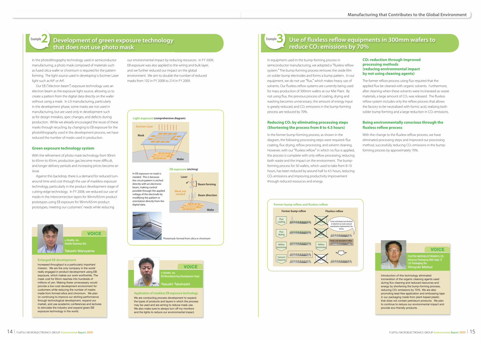
Development of green exposure technology that does not use photo mask
In the photolithography technology used in semiconductor manufacturing, a photo mask composed of materials such as fused silica wafer or chromium is required for the pattern forming. The light source used in developing is Excimer Laser light such as KrF or ArF. Our EB (“electron beam”) exposure technology uses an electron beam as the exposure light source, allowing us to create a pattern from the digital data directly on the wafer without using a mask. In LSI manufacturing, particularly in the development phase, some masks are not used in manufacturing, but are used only in development such as for design mistakes, spec changes, and defects during production. While we already encouraged the reuse of these masks through recycling, by changing to EB exposure for the photolithography used in the development process, we have reduced the number of masks used in production.
Green exposure technology system
With the re� nement of photo mask technology from 90nm to 65nm to 45nm, production gas become more di� cult, and longer delivery periods and increasing prices become an issue. Against this backdrop, there is a demand for reduced turn-around time and cost through the use of maskless exposure technology, particularly in the product development stage of cutting-edge technology. In FY 2008, we reduced our use of masks in the interconnection layers for 90nm/65nm product prototypes using EB exposure for 90nm/65nm product prototypes, meeting our customers’ needs while reducing
our environmental impact by reducing resources. In FY 2009, EB exposure was also applied to the wiring and bulk layer,and we further reduced our impact on the global environment. We aim to double the number of reduced masks from 102 in FY 2008 to 214 in FY 2009.
Example2
Photomask: formed from silica or chromium
In EB exposure no mask is needed. This is because the circuit pattern is etched directly with an electronic beam, making control possible through the applied voltage of the electrode by modifying the pattern or orientation directly from the digital data.
e-Shuttle, Inc.Shuttle Business Div.
Takashi Maruyama
Enlarged EB developmentIncreased throughput is a particularly important mission. We are the only company in the world really engaged in product development using EB exposure, which makes our work worthwhile. The mask cost for 65nm reaches into hundreds of millions of yen. Making these unnecessary would provide a low-cost development environment for customers while reducing the number of masks made from formed silica and chromium. We plan on continuing to improve our etching performance through technological development, expand our market, and use academic conferences and lectures to stimulate the industry and expand green EB exposure technology in the world.
VOICE
Light exposure (comprehensive diagram)
Excimer Laser
Mask
Wafer
EB exposure (etching)
Mask not needed
Laser
Wafer
e-Beam forming
Beam direction
}
Use of � uxless re� ow equipments in 300mm wafers to reduce CO2 emissions by 70%
In equipment used in the bump-forming process in semiconductor manufacturing, we adopted a “� uxless re� ow system.” The bump-forming process removes the oxide � lm on solder bump electrodes and forms a bump pattern. In our equipment, we do not use “� ux,” which makes heavy use of solvents. Our � uxless re� ow systems are currently being used for mass production of 300mm wafers at our Mie Plant. By not using � ux, the previous process of coating, drying and washing becomes unnecessary; the amount of energy input is greatly reduced; and CO2 emissions in the bump-forming process are reduced by 70%.
Reducing CO2 by eliminating processing steps(Shortening the process from 8 to 4.5 hours)
In the former bump-forming process, as shown in the diagram, the following processing steps were required: � ux coating, � ux drying, re� ow processing, and solvent cleaning. However, with our “� uxless re� ow” in which no � ux is applied, the process is complete with only re� ow processing, reducing both waste and the impact on the environment. The bump- forming process for 50 wafers, which used to take from 8-10 hours, has been reduced by around half to 4.5 hours, reducing CO2 emissions and improving productivity improvement through reduced resources and energy.
CO2 reduction through improved processing methods (reducing environmental impact by not using cleaning agents)
The former re� ow process using � ux required that the applied � ux be cleaned with organic solvents. Furthermore, after cleaning when these solvents were incinerated as waste materials, a large amount of CO2 was released. The � uxless re� ow system includes only the re� ow process that allows the factory to be neutralized with formic acid, realizing both solder bump forming and a large reduction in CO2 emissions.
Being environmentally conscious through the � uxless re� ow process
With the change to the � uxless re� ow process, we have eliminated processing steps and improved our processing method, successfully reducing CO2 emissions in the bump- forming process by approximately 70%.
Example3
FUJITSU MICROELECTRONICS LTD.Advance Packaging R&D Dept.ⅡLSI Packaging Div.
Hiroyuki Matsui
Introduction of this technology eliminated incineration of the organic cleaning agents used during fl ux cleaning and reduced resources and energy by shortening the bump-forming process, reducing CO2 emissions by 70%. We are also promoting lead-free application and embossing tape in our packaging made from plant-based plastic that does not contain petroleum products. We plan to continue to reduce our environmental impact and provide eco-friendly products.
VOICE
Former bump reflow and fluxless reflow
Former bump reflow
Fluxcoating
Fluxdrying
Reflowprocessing
Solventcleaning
Fluxless reflow
Formic acid atmosphere reflow
Fluxcoating
Fluxdrying
Reflowprocessing
Solventcleaning
Formic acid exhaust was dissolved in industrial-use water and acid
neutralization implemented in the factory
e-Shuttle, Inc.EB Manufacturing Development Dept.
Yasushi Takahashi
Application of maskless EB exposure technologyWe are conducting process development to expand the types of products and layers in which the process may be used and are aiming to reduce mask use. We also make sure to always turn off my monitors and the lights to reduce our environmental impact.
VOICE
14 | FUJITSU MICROELECTRONICS GROUP Environmental Report 2009 FUJITSU MICROELECTRONICS GROUP Environmental Report 2009 | 15

Manufacturing that Contributes to the Global Environment
Approach to the Environment
Green Factory and Green Offi ce
G lobal Warming Measures
Reduced resource usage (materials, water, natural energy, paperless operation)
Communication withthe local region
Environmental enlightenmentand education
Safe operation (environmental risk) Green purchasing
Soil and groundwatercontamination countermeasures
Chemicals andgreenhouse gases
Voluntary managementstandards
Energy savings and reduction of CO2 emissions
Waste reduction (zero emissions, recycling)
Activities that make contributions to society
Acquisition of ISO 14001 certification(EMS construction and operation), compliance with laws.
Unique item exam
plesRequired item
examples
One Star
Certi� cation level image
Three Stars Further points added for items
unique to the business site
★★★
Two StarsTargets achieved and basic levels
met for the required items (Each item is evaluated on a � ve-point scale in
which � ve is the best score).
★★
★
GreenFactory
GreenO� ce
Fujitsu Microelectronics Group works to reduce the greenhouse gases emitted in the business activities at our factories and o� ces. We are also making e� orts to prevent global warming in all areas of our business activities while contributing to the reduction of greenhouse gas emissions by our customers and society as a whole through the development of low-power IC products (see P.9).
Reduce emissions of CO2 from energy consumption
■ Basic philosophyFujitsu Microelectronics Group is working to reduce emissions of CO2 from energy consumption at our factories and o� ces by Fujitsu Group’s 5th Environmental Action Plan.■ FY 2008 resultsOur group implemented the following measures in FY 2008:
● Energy-saving measures centered on our machinery for power generation (Installation of energy-saving facilities, free cooling, etc.)
● Installation of co-generation conversion facilities ● Improved e� ciency through manufacturing process review ● Appropriate o� ce temperature settings, energy saving with
lighting and o� ce equipmentAs a result of these e� orts, total CO2 emissions from energy consumption in FY 2008 was 529 thousand tons. This amounted to a 10% reduction from the previous � scal year.
In the 5th Environmental Action Plan created by the Fujitsu Group, we made it our goal that all business locations reach at least the 2-star level in the green factory or green o� ce system by the end of FY 2009. Fujitsu Microelectronics Group is utilizing this system not only in our factories, but in our o� ces as well. By comprehensively evaluating the level of environmental friendliness and the independent e� orts of our business locations, we are working to continually improve environmental friendliness.
Environmental IC packages
In the design of IC packages, use of packaging technology that introduces cutting-edge technology reduced the total number of parts and lowered the environmental impact. We also o� er a wide package lineup, providing the optimal package for our customers’ needs. Furthermore, we provide information on the chemical substances our products contain.
High-density packaging through leading technology and comprehensive design, packages that achieve reduced component materials
Multiple IC chips are stacked and combined in one package. The structure (SiP*, PoP*) also incorporates peripheral parts, achieving ultra-high-density packaging. A large reduction in materials is also possible. Furthermore, by optimizing the structure, thermal dissipation is improved, and the heat sink that used to be required can be eliminated, enabling it to be embedded inside the package (TEQFP, TEBGA) or enabling the same-size IC chip to be loaded directly in a chip size package (WL-CSP), reducing the environmental impact in various ways.* SiP: System in package* PoP: Package on package.
Example 4
IC chip size mounting possibleWL-CSP
Heat spreaderembeddedTEBGA
Package on packagePackage on Package
Chip embedded in packageEmbedded Package
Different types of chips layeredSystem in Package
BGA-Type QFP-Type
Embedded chip exposedon baseTEQFP
Resistor or capacitor embedded in moduleModule Package
Face Base
FUJITSU MICROELECTRONICS LTD.Product Development Dept.LSI Packaging Div.
Akihiko Murata
As the regulatory and market demands on the chemical substances included in our products increase, I believe that developing technology to reduce the impact on the environment and providing information related to the environment is our corporate responsibility. Responses based on REACH have become the norm of late, and an effi cient and precise response is important. We are always conscious of reducing our environmental burden during package development.
VOICE● Emissions of CO2 from energy consumption
ResultBase level Goal
20
40
60
02007 2008 2010
58.652.9 52.7
(FY)
10
30
50
(CO2 ten thousand of tons)
70
16 | FUJITSU MICROELECTRONICS GROUP Environmental Report 2009 FUJITSU MICROELECTRONICS GROUP Environmental Report 2009 | 17

FUJITSU FACILITIES ENGINEERING LTD.Engineering Dept.Aizuwakamatsu Offi ce
Yoshinori Ozawa
Every day through trial and error we aim to optimize operations of the super-clean-room climate-control equipment at the Fujitsu Microelectronics Aizu-Wakamatsu plant to minimize the effect on products and reduce energy consumption as much as possible. We also try to conserve energy in our everyday lives, never forgetting to unplug.
We are working to reduce the materials used, and chemicals and waste emitted, by our business processes and to minimize manufacturing costs.
Chemical substances management
■ Basic philosophyAs a member of the Fujitsu Group, based on the chemical substance management guidelines of “preventing environmental risks from the use of hazardous chemical substances that can lead to pollution of the natural environment and health hazards,” we manage the use of chemical substances at our business locations and work to reduce and appropriately manage emissions.■ FY 2008 resultsIn according with the 5th Environmental Action Plan of the Fujitsu Group, our group is working to reduce atmospheric emissions of VOC (volatile organic compounds) at our business locations. In FY 2008, group-wide VOC atmospheric emissions totaled 150 tons. This was a 4% increase from the previous � scal year, but in FY 2009 we plan to work to reduce emissions by increasing the e� ciency of organic solvent collection equipment and promoting the thorough and appropriate management of VOC substances.
Reducing the amount of waste generated
■ Basic philosophyAs a member of the Fujitsu Group, based on the basic guidelines of the 3Rs (Reduce, Reuse, Recycle) to create a recycling-based society, we are promoting the separation of waste by each employee to take an even more elevated approach to the 3Rs.■ FY 2008 resultsIn keeping with the 5th Environmental Action Plan of the Fujitsu Group, our group is working to reduce the waste generated by our business locations. In FY 2008, group-wide waste generation totaled 11,000 tons. This was a 22% decrease from the previous � scal year. This was due to not only to converting things like waste plastic and waste acid into valuable resources, but also to signi� cant market changes.
Reduction of greenhouse gases other than CO2
■ Basic philosophyFujitsu Microelectronics Group follows Fujitsu Group’s 5th Environmental Action Plan and action plans established independently by the semiconductor industry for the reduction of greenhouse gases such as PFCs, HFCs and SF6 in factories.■ FY 2008 resultsIn FY 2008, with assistance from NEDO (New Energy and Industrial Technology Development Organization, an independent administrative agency in Japan), we set up PFC gas removal systems at new and existing manufacturing lines and converted to gases with lower global warming potential. As a result of these e� orts, our group-wide emissions in FY 2008 fell to 428,000 tons after conversion using the global warming potential index (GWP). This represented a 22% reduction from the previous � scal year.
C hemical and Waste Reduction Measures
Approach to the Environment
E nvironmental Risk Management
Comprehensive risk response
Our group has always identi� ed natural risks (e.g., earthquakes, typhoons) and latent risks such as environment pollution caused by aging plant buildings and environmental facilities, assigned priorities and implemented scheduled improvements. In FY 2008, we also began to evaluate these latent risks from the standpoint of “business continuity.” We plan to continue our activities to decrease risk.
Response to soil and groundwater pollution issues
Our group monitors the groundwater on the grounds of our facilities based on the “soil and groundwater survey, response and disclosure regulations” set forth by the Fujitsu Group. We will continue our monitoring, cleanup and response based on the situation at the business location in the event pollution has been veri� ed, and coordinate with public administration to disclose information.
Soil and groundwater surveys and response
As the result of an independent survey at the Mie Plant, � uoride contamination in the groundwater and lead contamination in the soil were discovered and reported to public administration. As this pollution was discovered in the center of the plant grounds, there were no problems with the groundwater at the border line of the lot. The groundwater pollution was discovered in the standing water of a detection hole (a hole several meters deep dug near the plant to detect leaks in underground holding tanks and pipes) at the plant. However, a comprehensive survey of the history of the land use and chemical substances, determined that the soil pollution was caused naturally. In this case, we reported the pollution situation and our response to the neighboring residents and relevant administration. Furthermore, with the closing of the Fujitsu Integrated Microtechnology Ltd. Monden Plant, as a result of a survey based on the Article 3 of the Soil Contamination Countermeasures Act, it was determined that there was no soil pollution. This result was reported to the relevant administration.
Managing PCB waste
For equipment containing PCBs (see chart below) based on the Law Concerning Special Measures Against PCB Waste (PCB Law), each plant reports the quantity to the relevant administration and carefully stores the waste. Furthermore, for highly concentrated PCB waste whose processing method is stipulated by the PCB Law, we have already completed early registration with the PCB waste processing company Japan Environmental Safety Corporation. The waste will be processed one by one based on the plan.
PFC gas abatement equipment
● Emissions of greenhouse gases other than CO2
(GWP ten thousand of tons)
Base level Result
20
40
60
01995 2005 2006 2007 2008
25.9
48.8
38.1
54.9
42.8
(FY)
10
30
50
2010
23.3
Goal
VOICE
TypeStorage amount (units)
HighPCB concentration
LowPCB concentration
Transformer 0 20
Capacitor 22 5
Fluorescent ballasts 0 1,875
18 | FUJITSU MICROELECTRONICS GROUP Environmental Report 2009 FUJITSU MICROELECTRONICS GROUP Environmental Report 2009 | 19

Environmental conservation activities
Our group’s employees also participate in the Fujitsu Group group-wide activities such as tree planting and forest conservation. Overseas, with the goal of restoring the rainforest in Borneo, Malaysia, we have planted dipterocarp, an old-growth species. Through continued tree-planting activities, several species of birds and monkeys that had disappeared from the rainforest have returned. In Japan, we are involved in conservation activities such as thinning operations and preparing areas for Shiitake mushrooms to grow in the Hachioji Tobuki Northern Woods Conservation Area.
Fujitsu Microelectronics Group works to ensure that each of us acts as a “good member of society” even before acting as an employee, aiming for mutually beneficial relationships with both the international and local communities.
Environmental Communication
Approach to the Environment
E nvironmental Social Contribution
Fujitsu Microelectronics Group, as a member of society, contributes to the local community through environmental social contributions such as regional cleanup activities and tree planting activities. Furthermore, recognizing the importance of the natural environment, our employees participate in environmental conservation activities to preserve nature for the next generation and give lessons on the environment to children of neighborhood schools. Through regional contribution activities, environmental conservation activities and environmental education activities, we continue to deepen exchanges with the international and local community and promote broad social contribution activities.
Regional contribution activities
Woodland conservation activities
Tree planting activities in Malaysia
Tree planting activities in Hong Kong (FUJITSU MICROELECTRONICS ASIA LTD.)
Eco Cap Program(FUJITSU LSI TECHNOLOGY LTD.)
Planting lavender seedlings (Aizuwakamatsu Plant)
Park Adapt Program (Mie Plant)
Meetings to read environmental reports that start in the community (Iwate Plant)
Shin-Yokohama IT Cluster Exchange(FUJITSU MICROELECTRONICS SOLUTIONS LTD.)
Misaka Kogen Clean Health Walk(FUJITSU SEMICONDUCTOR TECHNOLOGY, INC.)
FUJITSU INTEGRATED MICROTECHNOLOGY LTD.Manufacturing Dept.ⅠENVN Products Manufacturing Div.
Katsuichi Nishi
I am in charge of the process control for the back-end of the semiconductor manufacturing at our plant. At the factory, to contribute to energy saving and reduce costs, the rule is to turn off power in idle equipment and turn off ancillary equipment on our microscope when not in use. We also reduce waste by distributing only a fi xed number of masks and checking for air leaks, preventing wasted resources and costs. Also, we work daily to actively do what we can to “prevent global warming” and “go easy on our wallets” by, for example, using a broom whenever possible to avoid using a vacuum cleaner, and using rainwater to water fl owers.
Environmental education activities
Fujitsu VLSI Limited and Fujitsu Microelectronics Akiruno Technology Center visit schools to give environmental lessons to children. At elementary schools, children take apart computers to learn about the 3Rs (Reduce, Reuse, Recycle) and deepen their understanding of the environment.
E xternal Awards and Environmental Awareness
We would like to introduce the various awards Fujitsu Microelectronics Group has received for its environmental activities and our employee environmental awareness activities centered on our FY 2008 activities.
External Awards
Fujitsu Microelectronics and Fujitsu LSI Solutions Limited were awarded 2nd Place in the 2009 “Semiconductor of the Year” contest held by The Semiconductor Industry News for their ultra-high-speed security processor (MB86C61/60A). Our group received the “Award for 10 Years of a Continued Environmental Management System" from the Japan Audit and Certi� cation Organization. This was given to entities that acquired certi� cation prior to March 1999 and continue their environmental activities today. Entities that received the award included Fujitsu Microelectronics (Iwate Plant, Aizu-Wakamatsu Plant, Mie Plant), Fujitsu Integrated Microtechnology Ltd. (Aizu Plant, Miyagi Plant, Kyushu Plant) and Fujitsu VLSI Limited.
Looking to win the Flower Garden Contest for the third straight yearWe enter the “Flower Garden Contest” held by Aizuwakamatsu city every year and received the highest award two years in a row from 2007 to 2008. A theme is selected at the start of each year, and in 2009 we began our � ower garden design with the theme of “refreshing summer colors.” We are working hard to win for the third straight year.
Distribution of organic fertilizers to local communitiesAt the Miyagi Plant, raw garbage from the employee cafeteria is turned into fertilizer and distributed by employees to elementary and middle schools and the local soba producer association in the local town of Murata, deepening our relationship with the local community.
Participation in local eco-forumsIn Miyagi Prefecture, companies from di� erent industries get together in di� erent areas, and eco-forum activities are conducted to share environmental information and contribute to the local community. At the Miyagi Plant, we participate in the “Murata, Ogawara, Shibata Eco-Forum” to promote community exchange on the environment.
Environmental lesson
FUJITSU INTEGRATED MICROTECHNOLOGY LTD.
FUJITSU SEMICONDUCTOR TECHNOLOGY, INC.
VOICE
20 | FUJITSU MICROELECTRONICS GROUP Environmental Report 2009 FUJITSU MICROELECTRONICS GROUP Environmental Report 2009 | 21

under the umbrella of the Fujitsu Group comprehensive EMS. We are making preparations to consolidate EMS in our group as well, to increase the sense of solidarity in semiconductor-focused environmental activities.
ISO14001 certi� cation acquisition and environmental audits
At the end of FY 2004, Fujitsu Group acquired the international EMS standard ISO14001 for its domestic consolidated subsidiaries, and was conducting environmental activities based on the management system at a total of 97 Fujitsu and domestic group companies and 11 overseas group companies acquired the global uni� cation certi� cation in FY 2005. Furthermore, to ensure the objectivity and independence of internal audits at the Fujitsu Group, a Management Audit Division that belongs to neither reporting line took the central role in gathering auditors from Fujitsu and Group companies to conduct internal audits. Our group implemented internal audits at our domestic manufacturing and o� ce locations and overseas sales locations in FY 2008, identifying 12 minor nonconformances and making 33 observations, all of which were corrected by April 2009.
Fujitsu Microelectronics Group participates in the comprehensive environmental activities of the Fujitsu Group, and all of its domestic group companies and many of its overseas groups companies have received ISO14001 certi� cation. We promote environmental management through the operation of the environmental management systems, e� orts toward continual improvement, environmental audits and environmental education.
Environmental management system
In order to respond quickly to executive decisions, Fujitsu Group’s environmental management system (EMS) combines line activities to promote environmental conservation activities in line with the characteristics of each business based on the organization of each business, and site activities for themes that are shared by each factory and o� ce. Our � rm and our group companies conduct similar activities
Approach to the Environment
Environmental awareness activities
To increase the environmental awareness of each employee of Fujitsu Microelectronics Group, we conduct various environmental education and environmental awareness activities. In addition, we also participate in the Fujitsu Group-wide education menu such as “environmental e-learning” and “waste management representative seminars” given by external lecturers. Furthermore, group companies also o� er independent environmental education. In our environmental month, we conduct workshops through video, to help learn about everyday environmental activities such as container recycling, and to heighten environmental awareness. We also conduct tours of environmental facilities, small environmental exhibits and environmental seminars such as “The Current State and Function of the Forests, What We Can Do,” given by external lecturers.
Environmental Management System
Based on the frame-work of the Fujitsu Group environmental management system founded on ISO14001, we are working to improve the environmental impact unique to the semiconductor industry and improve the environmental characteristics of the semiconductor products we provide to our customers.
E nvironmental Management
F Y 2008 Results
Fujitsu Microelectronics Group has established clear targets that take into account all group business areas based on the Stage V Fujitsu Group Environmental Protection Plan, and is taking a planned and continual approach to environmental conservation activities. In FY 2008, yearly objectives for all seven categories were achieved. The Stage V Environmental Protection Plan was concluded in FY 2009. To achieve the mid-term plan, the group must come together thorough environmental management.
Outstanding results for FY 2008
In FY 2008, we paid particular attention to “greenhouse gases other than CO2 greenhouse reduction.” This gas is unique to semiconductor manufacturing, so we strongly believe that we have to reduce it.
We produced great results from our improvement e� orts, and received 1st Place in the FY 2008 Fujitsu Group Environmental Contribution Awards. This was a case in which the environmental management system activities produced great results.
● Stage V Fujitsu Group Environmental Protection Plan Progress in FY 2008
Improving the environmental
value of products and services
Global warming countermeasures
Environmental contributions
to society
Stage V Environmental Protection Plan Targets
【Increase the number of Super Green Products】Targeting the Green Products being newly developed in all business units, by the end of FY 2009 we aim to increase by over 50% the proportion of products that are Super Green Products with top-class environmental characteristics.● FML Group working for an environmental target of 100% (all 9 products).
【Achieve an improved environmental e� ciency factor】By FY 2009 we will strive to achieve an environmental e� ciency factor of “2” relative to products in FY 2005 for newly developed Green Products in all business units.● FML Group working for an environmental target of “1.5”.
【Reduce greenhouse gases other than CO2】We will work to reduce emissions of greenhouse gases other than CO2 by 10% relative to FY 1995 emissions by the end of � scal 2010.● FML Group working for an environmental target of reducing emissions to 233,000 tons GWP in FY 2010 compared to 259,000 tons GWP in FY 1995.
【Reduce VOC emissions】We aim to reduce volatile organic compound (VOC) emissions by 30% relative to FY 2000 levels by FY 2009.● FML Group working for an environmental target of reducing emissions to 130 tons in FY 2009 compared to 110 tons in 2000.
【Reduce waste generation】We will strive to reduce waste generation by 3% relative to 2005 levels by the end of FY 2009.● FML Group working for an environmental target of 10,000 tons of waste in FY 2009 compared to 13,000 tons in FY 2005.
【Activities for environmental contributions to society】We will carry out locally attuned activities that make environmental contributions to society and in which each of our employees can play an important role.
More than 33% (created two product series)
Achieve environmental e� ciency factor of 1.4
Reduce CO2 emissions to below 600,000 tons
Reduce PFC emissions to below 622,000 tons
Reduce VOC emissions to below 230 tons
Reduce waste to below 16,000 tons
One environmental and social contribution activity implemented at each location yearly
Super Green Products created from two series
Achieved environmental e� ciency factor for target products of 1.95 and 6.67
CO2 emissions of 529,000 tons
FY 2008 PFC emissions of 428,000 tons
FY 2008 VOC emissions of 150 tons
FY 2008 waste of 11,000 tons
One social contribution activity is implemented at each FML group location yearly.
FML GroupFY 2008 Results
AchievementStatus
○
○
○
○
○
○
○
RelatedPage
6
7
17
18
18
18
20
FML GroupFY 2008 Targets
【Reduce CO2 emissions from energy consumption】Limit energy-consumption-related CO2 emissions at our business sites to below FY 1990 levels by the end of FY 2010.● FML Group working for an environmental target of a 10% reduction compared to FY 2007 (527,000 tons of CO2).
FUJITSU VLSI LTDDesign Dept.ⅠAnalog Products Development Div.
Kimitaka Yoshiyama
I am working on the “low-power design of automobile power ICs,” and through my work, I am trying to reduce my the environmental impact. I also conserve energy and recycle trash as part of my everyday environmental activities. While these may be small, by continuing with them I believe we can improve our living environment.
To enhance environmental awareness in primary operations, Fujitsu Microelectronics held an environmental lecture given by the head of Fujitsu’s Environmental Division entitled “The Role of the IT Industry in Preventing Global Warming.” More than 200 employees participated in the lecture, which connected the network between headquarters and the Sendai and Osaka business locations.
FUJITSU MICROELECTRONICS SOLUTIONS LTD.
(“FML Group” in the chart refers to Fujitsu Microelectronics Group)
VOICE
Five Priority Areas
22 | FUJITSU MICROELECTRONICS GROUP Environmental Report 2009 FUJITSU MICROELECTRONICS GROUP Environmental Report 2009 | 23

Approach to the Environment Fujitsu Microelectronics Group Corporate Pro� le
B usiness Activities and Environmental Impact (Material Balance)
Fujitsu Microelectronics Group quantitatively measures input and output in order to reduce the overall environmental impact generated at each stage of production. The promotion of Group-wide environmental management and environmentally friendly business activities is crucial to achieving this goal. It enables the Group to take a planned approach to the reduction of environmental impact related to materials procurement and the use of energy, water resources and chemical substances. Based on our environmental management system, through the entire lifecycle from product development and design to the collection and recycling/reuse of packing materials, we work to reduce our environmental impact while e� ectively using limited resources. And, by providing environmental semiconductors and electronic devices, we work to reduce the environmental impact of our customers’ product.
E nvironmental Accounting
Our group calculates the cost and economic bene� ts of our environmental activities in our business based on Fujitsu Group’s “Environmental Accounting Guidelines,” which implements environmental accounting that evaluates the e� ects of environmental investments. Through environmental accounting, the results of the evaluation are re� ected in group environmental management. Long-term, continual environmental policies are pursued, environmental investment made more e� cient and environmental conservation activities stimulated.
FY 2008 total results
As shown in the chart, group environmental accounting in FY 2008 resulted in capital expenditures of 259 million yen, costs of 3,689 million yen and economic bene� ts of 4,707 million yen.■ Amount of investmentIn FY 2008, investment focused on pollution prevention measures and global-warming-prevention measures (e.g., the installation of PFC removal systems).■ CostsWe are continuing to take a planned approach to making improvements in energy conservation and reduced waste measures, focused on air and water pollution costs (e.g., environmental analysis fees). Pollution prevention, environmental conservation and resource circulation cost are all part of the total cost because we use chemical substances, and processing the waste generated during and after the use of the chemical substances required for semiconductor manufacturing. However, by analyzing results of the environmental accounting totals, we are making e� cient environmental investments and reducing our environmental impact.
Note: Figures may not add to total due to rounding.
Unit: million yen● Fujitsu Microelectronics Group Environmental Accounting Total Results (FY 2008)
Corporate Profile
Survey Request
Thank you for reading “Fujitsu Microelectronics Group Environmental Report 2009.” To help us in creating the next report, we ask for your cooperation in completing the survey found on the following link. Those completing the survey will be sent a copy of “Fujitsu Microelectronics Group Environmental Report 2010.”
Survey link http://www.fujitsu.com/global/services/microelectronics/environment/
CO2 emissions529,219 t
NOx emissions148.9 t
SOx emissions55.7 t
Amount of waste generated
10,665 t
Waste water
12,576,136 m3
Chemical substances
3.5 t
OUTPUT
Purchased electricity
1,034,975 MWh
Heavy oil31,075 kl
Kerosene726 kl
City gas1,746,311 m3
LPG156 m3
Water13,280,293 m3
Chemical substances
557 t
INPUT
Fujitsu Microelectronics Group
Item Main areas covered Capitalinvestment Cost Economic
benefits
Business area costs/benefits
Pollution prevention cost/benefits Preventing air pollution/water pollution, etc. 63 1,744 1,557
Global environmental conservation cost/benefits Preventing global warming, saving energy, etc. 175 678 648
Resource circulation costs/benefits Disposal of waste, e� cient utilization of resources, etc. 0 839 2,216
Upstream/downstream cost/benefits Collection, recycling, reuse, and proper disposal of products, etc. 0 5 49
Administration cost/benefitsMaintenance and operation of environmental management systems, environmental education of employees, etc.
0 401 36
Research and development costs/benefits Research and development of products that contribute to environmental protection, etc. 0 0 1
Societal activity costs Donations to, and support for, environmentalgroups, etc. 0 0 0
Environmental remediation costs/benefits Restoration and other measures related to soil and groundwater contamination. 21 21 200
Total 259 3,689 4,707
Corporate name FUJITSU MICROELECTRONICS LIMITED
Location of head o� ce Nomura Fudosan Shin-yokohama Bldg. 10-23, Shin-yokohama 2-Chome, Kohoku-ku Yokohama Kanagawa 222-0033, Japan
President Haruki Okada
Date of establishment March 21, 2008
Business description Design, development, manufacturing, and sale of LSI products
Capital 60,000 million yen
Group companies FUJITSU MICROELECTRONICS LTD.
・Akiruno Technology Center
・Mie Plant
・Aizuwakamatsu Plant
・Iwate Plant
FUJITSU ELECTRONICS INC.
FUJITSU INTEGRATED MICROTECHNOLOGY LTD.
・Aizu Plant
・Miyagi Plant
・Kyushu Plant
FUJITSU VLSI LTD.
FUJITSU LSI TECHNOLOGY LTD.
FUJITSU LSI SOLUTIONS LTD.
FUJITSU MICROELECTRONICS SOLUTIONS LTD.
FUJITSU SEMICONDUCTOR TECHNOLOGY, INC.
e-Shuttle, Inc.
FUJITSU FACILITIES ENGINEERING LTD.
FUJITSU MICROELECTRONICS AMERICA, INC.
FUJITSU MICROELECTRONICS EUROPE GmbH
FUJITSU MICROELECTRONICS ASIA PTE. LTD.
FUJITSU MICROELECTRONICS PACIFIC ASIA LTD.
FUJITSU MICROELECTRONICS (SHANGHAI) CO., LTD.
FUJITSU MICROELECTRONICS KOREA LTD.
FUJITSU GLOBAL MOBILE PLATFORM INC.
24 | FUJITSU MICROELECTRONICS GROUP Environmental Report 2009 FUJITSU MICROELECTRONICS GROUP Environmental Report 2009 | 25