four-dimensional ultrafast electron microscopy of phase ... · four-dimensional ultrafast electron...
TRANSCRIPT
Four-dimensional ultrafast electron microscopyof phase transitionsMichael S. Grinolds, Vladimir A. Lobastov, Jonas Weissenrieder, and Ahmed H. Zewail†
Physical Biology Center for Ultrafast Science and Technology, California Institute of Technology, Pasadena, CA 91125
Contributed by Ahmed H. Zewail, October 18, 2006 (sent for review October 17, 2006)
Reported here is direct imaging (and diffraction) by using 4Dultrafast electron microscopy (UEM) with combined spatial andtemporal resolutions. In the first phase of UEM, it was possible toobtain snapshot images by using timed, single-electron packets;each packet is free of space–charge effects. Here, we demonstratethe ability to obtain sequences of snapshots (‘‘movies’’) withatomic-scale spatial resolution and ultrashort temporal resolution.Specifically, it is shown that ultrafast metal–insulator phase tran-sitions can be studied with these achieved spatial and temporalresolutions. The diffraction (atomic scale) and images (nanometerscale) we obtained manifest the structural phase transition withits characteristic hysteresis, and the time scale involved (100 fs) isnow studied by directly monitoring coordinates of the atomsthemselves.
imaging � diffraction � electron crystallography � vanadium dioxide
E lectron microscopy has become a pivotal tool in numerousfields of study, from materials to biological imaging. In a
previous publication (1), we introduced the concept of single-electron imaging for the development of 4D ultrafast electronmicroscopy (UEM). The potential of UEM was demonstrated byobtaining images and diffraction patterns of materials andbiological cells (1), and the scope of future applications has beenhighlighted in recent commentaries and reviews (refs. 2 and 3;see also ref. 4 and references therein). Because single-electronpackets have no significant space–charge broadening, imagesand diffraction patterns are observed with atomic-scale spatialresolution and with the time resolution being fundamentallydetermined by the ultrashort duration of the optical pulseintroduced to generate the photoelectrons in the microscope.
The images and diffraction patterns reported (1) were ‘‘snap-shots’’ at a particular point in time. However, as shown in Fig. 1,by delaying a second initiating optical pulse to arrive at thesample in the microscope with controlled time steps, it is possibleto obtain a series of such snapshots with a well defined frametime. Unlike optical pump–probe experiments, this experimentaltask, for the microscope, is technically nontrivial for a numberof reasons. To determine the zero time point, the clocking of theelectron packet and optical pulse at the sample must be madewith femtosecond time precision. Moreover, in contrast to theseall-optical experiments, the cross-correlation between electronand photon pulses requires a new methodology. In addition, for120-keV electrons, the group velocity of electron packets in themicroscope is two-thirds the speed of light, and care has to betaken to account for this group velocity mismatch. Overcomingthese hurdles in conjunction with attaining high quality, nanom-eter-scale samples in the microscope provides the capability ofobserving the dynamical changes of systems in the far-from-equilibrium state with the combined resolutions mentionedabove.
With the 4D UEM arrangement shown in Fig. 1, we demon-strate such studies of imaging and diffraction for the metal–insulator phase transition in vanadium dioxide (VO2). Based onthe difference in conductivity the transition is termed metal–insulator, but when considering other properties it is referred toas a metal–semiconductor transition. The dioxide exhibits an
ultrafast transition and is an archetypical candidate for UEMstudy. Moreover, it is a strongly correlated system, and theinterplay of electron correlations and nuclear motion is criticalto the global dynamics of the phase transition. The material VO2undergoes a first-order phase transition from a low-temperaturemonoclinic (M) phase to a high-temperature tetragonal rutile(R) phase at �67°C (5, 6). Since its discovery almost half acentury ago, this phase transition has been the subject of intensestudy (6–8).
A widely accepted picture of the energy band diagram of theelectronic structure was presented early by Goodenough (9) andis based on an orbital description. In the monoclinic phase (spacegroup P21/c), the formation of V–V pairs and the tilting of thesedimers with respect to the rutile c axis completely destroys thesymmetry of the VO6 octahedron, which results in the splittingof the d� manifold into a lower-energy, filled bonding (3d�) andhigher-energy, empty antibonding (3d*�) state. The antibonding�* orbitals are pushed higher in energy because of the antifer-roelectric tilting of the V dimers, which increases the overlapwith the O 2p states. As a result, a band gap emerges, and a single3d electron of V occupies the bonding d� combination (9). In therutile phase (space group P42/mnm), VO6 octahedra form anedge-sharing chain along the c axis. The important feature hereis the degeneracy of the 3d� states and the lowering of the �*orbitals to be partly filled below the Fermi level.
There are a number of issues that remain unclear and requiredirect knowledge of structural dynamics. One issue is the exactnature of the energy gap, Peierls (9–11), or Mott–Hubbard (12,13) type; in other words, the role of electron correlations mustbe elucidated in the description of the band structure. The actualelectron–nuclear forces responsible for the change of structurefrom one phase to another must account for the ultrafasttransformation. Recent studies considered both electron corre-lations within the V–V pairs and structural effects and success-fully reproduced experimental data of photoemission and near-edge x-ray absorption fine structure spectra (14, 15). The phasetransition is described as a correlation-assisted Peierls transition.In other words, the M phase can be described as a renormalizedPeierls insulator at low energies and a Mott–Hubbard insulatorat high energy (14).
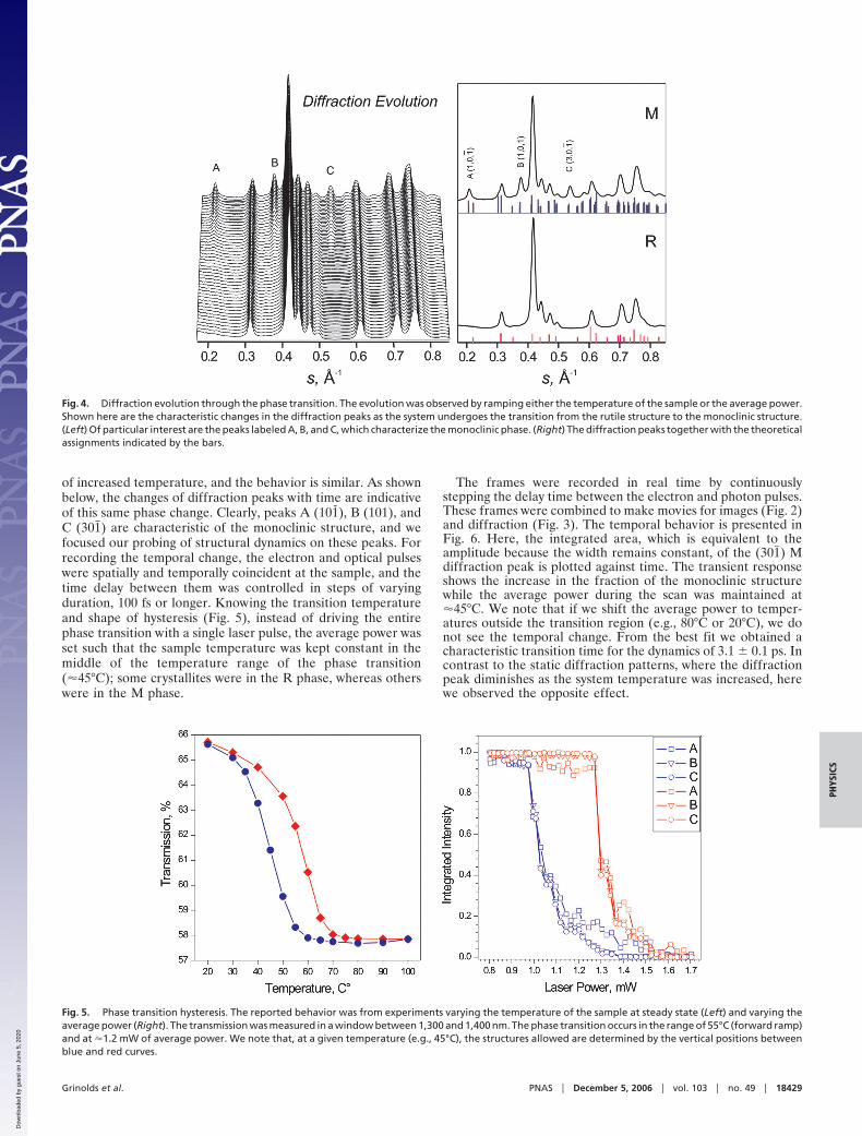
Results and DiscussionFig. 2 shows UEM real-space images obtained for the two phasesof the transition: metallic (R) and insulator (M). With themicroscope operating in the selected-area electron diffractionmode, we acquired the patterns in Fig. 3 before and after thetransition. These images and diffraction patterns were obtainedwhen the VO2 films were driven through the transition by theheat deposited from the ramped, initiating (near infrared) laser
Author contributions: M.S.G., V.A.L., J.W., and A.H.Z. performed research and wrote thepaper.
The authors declare no conflict of interest.
Abbreviation: UEM, ultrafast election microscopy; M, monoclinic; R, rutile.
†To whom correspondence should be addressed. Email: [email protected].
© 2006 by The National Academy of Sciences of the USA
www.pnas.org�cgi�doi�10.1073�pnas.0609233103 PNAS � December 5, 2006 � vol. 103 � no. 49 � 18427–18431
PHYS
ICS
Dow
nloa
ded
by g
uest
on
June
5, 2
020
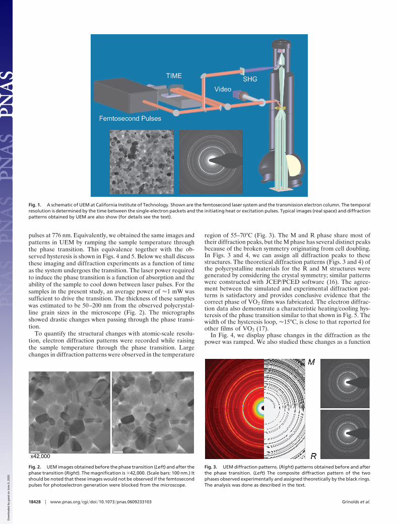
pulses at 776 nm. Equivalently, we obtained the same images andpatterns in UEM by ramping the sample temperature throughthe phase transition. This equivalence together with the ob-served hysteresis is shown in Figs. 4 and 5. Below we shall discussthese imaging and diffraction experiments as a function of timeas the system undergoes the transition. The laser power requiredto induce the phase transition is a function of absorption and theability of the sample to cool down between laser pulses. For thesamples in the present study, an average power of �1 mW wassufficient to drive the transition. The thickness of these sampleswas estimated to be 50–200 nm from the observed polycrystal-line grain sizes in the microscope (Fig. 2). The micrographsshowed drastic changes when passing through the phase transi-tion.
To quantify the structural changes with atomic-scale resolu-tion, electron diffraction patterns were recorded while raisingthe sample temperature through the phase transition. Largechanges in diffraction patterns were observed in the temperature
region of 55–70°C (Fig. 3). The M and R phase share most oftheir diffraction peaks, but the M phase has several distinct peaksbecause of the broken symmetry originating from cell doubling.In Figs. 3 and 4, we can assign all diffraction peaks to thesestructures. The theoretical diffraction patterns (Figs. 3 and 4) ofthe polycrystalline materials for the R and M structures weregenerated by considering the crystal symmetry; similar patternswere constructed with JCEP/PCED software (16). The agree-ment between the simulated and experimental diffraction pat-terns is satisfactory and provides conclusive evidence that thecorrect phase of VO2 films was fabricated. The electron diffrac-tion data also demonstrate a characteristic heating/cooling hys-teresis of the phase transition similar to that shown in Fig. 5. Thewidth of the hysteresis loop, �15°C, is close to that reported forother films of VO2 (17).
In Fig. 4, we display phase changes in the diffraction as thepower was ramped. We also studied these changes as a function
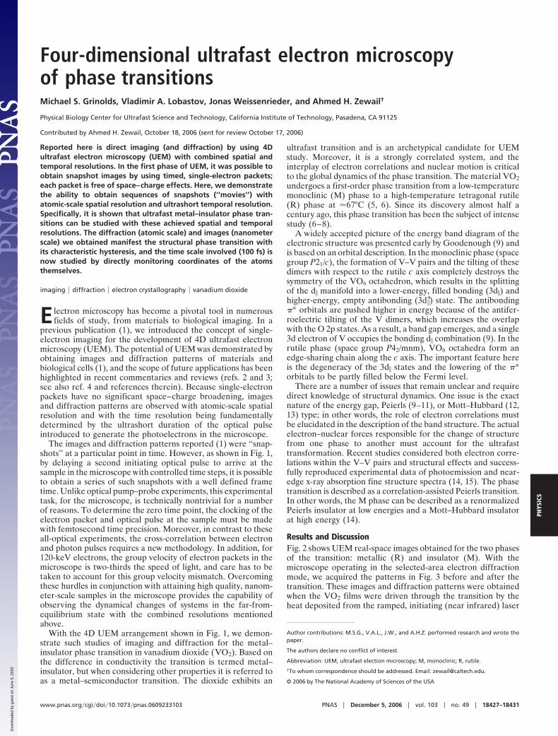
Fig. 1. A schematic of UEM at California Institute of Technology. Shown are the femtosecond laser system and the transmission electron column. The temporalresolution is determined by the time between the single-electron packets and the initiating heat or excitation pulses. Typical images (real space) and diffractionpatterns obtained by UEM are also show (for details see the text).
Fig. 2. UEM images obtained before the phase transition (Left) and after thephase transition (Right). The magnification is �42,000. (Scale bars: 100 nm.) Itshould be noted that these images would not be observed if the femtosecondpulses for photoelectron generation were blocked from the microscope.
Fig. 3. UEM diffraction patterns. (Right) patterns obtained before and afterthe phase transition. (Left) The composite diffraction pattern of the twophases observed experimentally and assigned theoretically by the black rings.The analysis was done as described in the text.
18428 � www.pnas.org�cgi�doi�10.1073�pnas.0609233103 Grinolds et al.
Dow
nloa
ded
by g
uest
on
June
5, 2
020
of increased temperature, and the behavior is similar. As shownbelow, the changes of diffraction peaks with time are indicativeof this same phase change. Clearly, peaks A (101), B (101), andC (301�) are characteristic of the monoclinic structure, and wefocused our probing of structural dynamics on these peaks. Forrecording the temporal change, the electron and optical pulseswere spatially and temporally coincident at the sample, and thetime delay between them was controlled in steps of varyingduration, 100 fs or longer. Knowing the transition temperatureand shape of hysteresis (Fig. 5), instead of driving the entirephase transition with a single laser pulse, the average power wasset such that the sample temperature was kept constant in themiddle of the temperature range of the phase transition(�45°C); some crystallites were in the R phase, whereas otherswere in the M phase.
The frames were recorded in real time by continuouslystepping the delay time between the electron and photon pulses.These frames were combined to make movies for images (Fig. 2)and diffraction (Fig. 3). The temporal behavior is presented inFig. 6. Here, the integrated area, which is equivalent to theamplitude because the width remains constant, of the (301�) Mdiffraction peak is plotted against time. The transient responseshows the increase in the fraction of the monoclinic structurewhile the average power during the scan was maintained at�45°C. We note that if we shift the average power to temper-atures outside the transition region (e.g., 80°C or 20°C), we donot see the temporal change. From the best fit we obtained acharacteristic transition time for the dynamics of 3.1 � 0.1 ps. Incontrast to the static diffraction patterns, where the diffractionpeak diminishes as the system temperature was increased, herewe observed the opposite effect.
Fig. 4. Diffraction evolution through the phase transition. The evolution was observed by ramping either the temperature of the sample or the average power.Shown here are the characteristic changes in the diffraction peaks as the system undergoes the transition from the rutile structure to the monoclinic structure.(Left) Of particular interest are the peaks labeled A, B, and C, which characterize the monoclinic phase. (Right) The diffraction peaks together with the theoreticalassignments indicated by the bars.
Fig. 5. Phase transition hysteresis. The reported behavior was from experiments varying the temperature of the sample at steady state (Left) and varying theaverage power (Right). The transmission was measured in a window between 1,300 and 1,400 nm. The phase transition occurs in the range of 55°C (forward ramp)and at �1.2 mW of average power. We note that, at a given temperature (e.g., 45°C), the structures allowed are determined by the vertical positions betweenblue and red curves.
Grinolds et al. PNAS � December 5, 2006 � vol. 103 � no. 49 � 18429
PHYS
ICS
Dow
nloa
ded
by g
uest
on
June
5, 2
020
The above results indicate that the transition occurs as a resultof nonthermal excitation and that both the electron and opticalpulses must be coincident for the transition to occur. Afteradding energy to the system, we would have naively expectedfrom the hysteresis behavior (Fig. 4) that the transition wouldshift more toward the high-temperature R phase; instead, thecontribution of the low-temperature M phase is enhanced. Thistrend is further supported by the fact that, in a given pulse, theenergy fluence is not sufficient to cause a large thermal gradient.In addition, the recovery of the system in the time between pulses(12.5 ns) is not complete. Finally, the observed large changerequires the passage through the region of time zero and was notobserved when the delay time was set at negative or positivetimes or when the step size greatly exceeded the observed risetime.
The ultrafast temporal change is the result of dynamicalresponse in the phase transition region and must occur when theelectron packet and optical pulse are within the observedwindow of time (Fig. 6). Optical studies of the M–R transitionwith femtosecond time resolution have indicated from reflec-tivity measurements that the transition occurs in �100 fs in thinsamples (50 nm) (18). However, when the sample thickness wasincreased (200 nm film), a rise time of 2.9 ps was observed,
remarkably in close agreement with our reported rise time of 3.1ps. As mentioned above, we are observing the transition whenthe femtosecond optical and electron pulses are coincident.
The following picture of structural changes on the ultrashorttime scale is proposed. From the band structure (Fig. 7), the Mphase has a band gap defined primarily by the splitting of the 3dmanifold, and this gap is absent in the R phase. The initiatingpulse electron packet on the ultrashort time scale induces, bymomentum conservation, a transient stress in the nanometer-scale sample and as such leads to a nonequilibrium structurecompatible with the M phase in its electronic configuration. Theultrashort optical pulse assists the transition through excitationto the antibonding band manifold and phase transformationoccurs in 100 fs. Accordingly, the observed 3-ps rise time is thetransit time for the nonequilibrium structure.
The stress is a ‘‘pressure-type’’ wave that survives for a fewpicoseconds and its effect is either kinematical (elastic), byexpansion, or possibly by Jahn–Teller distortion (19). It is knownthat VO2 structure is sensitive to changes of pressure andcomposition (20). However, it is also possible that some stress iscaused by acoustic wave generation by the photon (with theelectron packet assisting the transition). The stress wave inmaterials and in the presence of dislocations will have to beformed in an �3-nm slab, given the known sound velocity in thematerial and the rise in �3 ps. We note that the excitation ofcarriers from below the Fermi level to the antibonding 3d*� bandis significant for electron correlation effects.
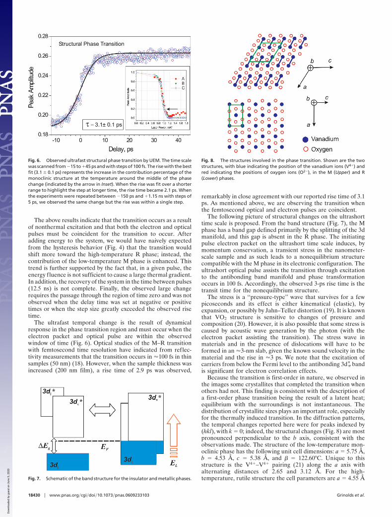
Because the transition is first-order in nature, we observed inthe images some crystallites that completed the transition whenothers had not. This finding is consistent with the description ofa first-order phase transition being the result of a latent heat;equilibrium with the surroundings is not instantaneous. Thedistribution of crystallite sizes plays an important role, especiallyfor the thermally induced transition. In the diffraction patterns,the temporal changes reported here were for peaks indexed by(hkl), with k � 0; indeed, the structural changes (Fig. 8) are mostpronounced perpendicular to the b axis, consistent with theobservations made. The structure of the low-temperature mon-oclinic phase has the following unit cell dimensions: a � 5.75 Å,b � 4.53 Å, c � 5.38 Å, and � � 122.60°C. Unique to thisstructure is the V4�–V4� pairing (21) along the a axis withalternating distances of 2.65 and 3.12 Å. For the high-temperature, rutile structure the cell parameters are a � 4.55 ÅFig. 7. Schematic of the band structure for the insulator and metallic phases.
Fig. 6. Observed ultrafast structural phase transition by UEM. The time scalewas scanned from �15 to �45 ps and with steps of 100 fs. The rise with the bestfit (3.1 � 0.1 ps) represents the increase in the contribution percentage of themonoclinic structure at the temperature around the middle of the phasechange (indicated by the arrow in Inset). When the rise was fit over a shorterrange to highlight the step at longer time, the rise time became 2.1 ps. Whenthe experiments were repeated between �150 ps and �1.15 ns with steps of5 ps, we observed the same change but the rise was within a single step.
Fig. 8. The structures involved in the phase transition. Shown are the twostructures, with blue indicating the position of the vanadium ions (V4�) andred indicating the positions of oxygen ions (O2�), in the M (Upper) and R(Lower) phases.
18430 � www.pnas.org�cgi�doi�10.1073�pnas.0609233103 Grinolds et al.
Dow
nloa
ded
by g
uest
on
June
5, 2
020
and c � 2.86 Å, with equivalent vanadium distances of 2.86 Å inthe chains of edge sharing VO2 octahedra. Through the phasetransition, the (100) plane in the monoclinic plane shifts by 0.43Å parallel to the (001) plane.
ConclusionThe results reported here demonstrate the ability of the single-electron, ultrafast electron microscope (1, 22) to record imagesand diffraction patterns with combined temporal and spatialresolutions. We demonstrated the application in the study ofmetal–insulator phase transitions. The observed temporalchange is evidence of a structural change from one phase to theother in a transition characterized by hysteresis. The temporalchanges of the images illustrate the size selectivity of thefirst-order phase transition on the nanometer-scale, whereas thechanges in the diffraction patterns provide the atomic-scalestructural determination. By increasing the fluence and timebetween pulses we should be able to map out the transition indifferent regions of the hysteresis and phases. We will alsocompare our UEM results with those obtained by using x-raydiffraction and optical studies (18, 25) and with those obtainedfor different composition materials.
Materials and MethodsPolycrystalline VO2 films were fabricated via a sol–gel method(23). The procedure was modified to provide an enhanced filmquality and more uniform composition. The precursor vanadylacetyl-acetonate (99.99% purity) (Sigma–Aldrich, St. Louis,MO) was dissolved in methanol and spin-coated onto a freshlycleaved mica substrate at 4,000 rpm for 20 s. The substrate wassubsequently heated to 80°C on a hot plate for 20 min to removeexcess solvent. At this point, an amorphous VO2 thin film hadformed on the substrate. To form the desired thermochromicphase, the samples were annealed for 2 h at 600°C in an N2environment. This step removed the remaining organics andtransformed the films into a polycrystalline aggregate of the VO2rutile structure. The films were then slowly cooled in an N2environment, yielding polycrystalline VO2 in the stable mono-clinic M phase.
The VO2 thin films were subsequently lifted off the micasubstrate in deionized water, placed onto a 300-mesh molybde-num grid and then immediately inserted into the UEM forcharacterization. Before the film liftoff, the thermochromic
activity and composition of the films were verified by opticaltransmission spectroscopy, and the transmission spectra of thefilms were measured as a function of temperature (Fig. 4). Aswas expected, the transmission sharply decreased in the near-infrared spectral region when passing through the insulator–metal phase transition between 50–70°C (24).
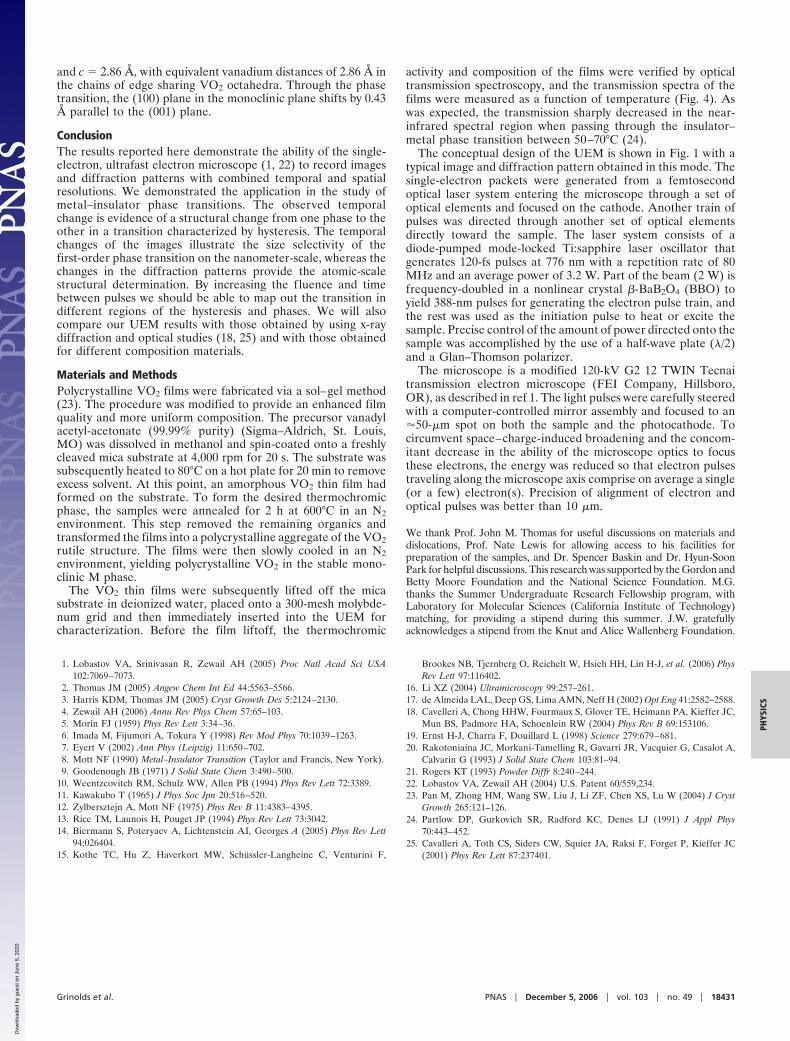
The conceptual design of the UEM is shown in Fig. 1 with atypical image and diffraction pattern obtained in this mode. Thesingle-electron packets were generated from a femtosecondoptical laser system entering the microscope through a set ofoptical elements and focused on the cathode. Another train ofpulses was directed through another set of optical elementsdirectly toward the sample. The laser system consists of adiode-pumped mode-locked Ti:sapphire laser oscillator thatgenerates 120-fs pulses at 776 nm with a repetition rate of 80MHz and an average power of 3.2 W. Part of the beam (2 W) isfrequency-doubled in a nonlinear crystal �-BaB2O4 (BBO) toyield 388-nm pulses for generating the electron pulse train, andthe rest was used as the initiation pulse to heat or excite thesample. Precise control of the amount of power directed onto thesample was accomplished by the use of a half-wave plate (�/2)and a Glan–Thomson polarizer.
The microscope is a modified 120-kV G2 12 TWIN Tecnaitransmission electron microscope (FEI Company, Hillsboro,OR), as described in ref 1. The light pulses were carefully steeredwith a computer-controlled mirror assembly and focused to an�50-�m spot on both the sample and the photocathode. Tocircumvent space–charge-induced broadening and the concom-itant decrease in the ability of the microscope optics to focusthese electrons, the energy was reduced so that electron pulsestraveling along the microscope axis comprise on average a single(or a few) electron(s). Precision of alignment of electron andoptical pulses was better than 10 �m.
We thank Prof. John M. Thomas for useful discussions on materials anddislocations, Prof. Nate Lewis for allowing access to his facilities forpreparation of the samples, and Dr. Spencer Baskin and Dr. Hyun-SoonPark for helpful discussions. This research was supported by the Gordon andBetty Moore Foundation and the National Science Foundation. M.G.thanks the Summer Undergraduate Research Fellowship program, withLaboratory for Molecular Sciences (California Institute of Technology)matching, for providing a stipend during this summer. J.W. gratefullyacknowledges a stipend from the Knut and Alice Wallenberg Foundation.
1. Lobastov VA, Srinivasan R, Zewail AH (2005) Proc Natl Acad Sci USA102:7069–7073.
2. Thomas JM (2005) Angew Chem Int Ed 44:5563–5566.3. Harris KDM, Thomas JM (2005) Cryst Growth Des 5:2124–2130.4. Zewail AH (2006) Annu Rev Phys Chem 57:65–103.5. Morin FJ (1959) Phys Rev Lett 3:34–36.6. Imada M, Fijumori A, Tokura Y (1998) Rev Mod Phys 70:1039–1263.7. Eyert V (2002) Ann Phys (Leipzig) 11:650–702.8. Mott NF (1990) Metal–Insulator Transition (Taylor and Francis, New York).9. Goodenough JB (1971) J Solid State Chem 3:490–500.
10. Weentzcovitch RM, Schulz WW, Allen PB (1994) Phys Rev Lett 72:3389.11. Kawakubo T (1965) J Phys Soc Jpn 20:516–520.12. Zylbersztejn A, Mott NF (1975) Phys Rev B 11:4383–4395.13. Rice TM, Launois H, Pouget JP (1994) Phys Rev Lett 73:3042.14. Biermann S, Poteryaev A, Lichtenstein AI, Georges A (2005) Phys Rev Lett
94:026404.15. Kothe TC, Hu Z, Haverkort MW, Schussler-Langheine C, Venturini F,
Brookes NB, Tjernberg O, Reichelt W, Hsieh HH, Lin H-J, et al. (2006) PhysRev Lett 97:116402.
16. Li XZ (2004) Ultramicroscopy 99:257–261.17. de Almeida LAL, Deep GS, Lima AMN, Neff H (2002) Opt Eng 41:2582–2588.18. Cavelleri A, Chong HHW, Fourmaux S, Glover TE, Heimann PA, Kieffer JC,
Mun BS, Padmore HA, Schoenlein RW (2004) Phys Rev B 69:153106.19. Ernst H-J, Charra F, Douillard L (1998) Science 279:679–681.20. Rakotoniaina JC, Morkani-Tamelling R, Gavarri JR, Vacquier G, Casalot A,
Calvarin G (1993) J Solid State Chem 103:81–94.21. Rogers KT (1993) Powder Diffr 8:240–244.22. Lobastov VA, Zewail AH (2004) U.S. Patent 60/559,234.23. Pan M, Zhong HM, Wang SW, Liu J, Li ZF, Chen XS, Lu W (2004) J Cryst
Growth 265:121–126.24. Partlow DP, Gurkovich SR, Radford KC, Denes LJ (1991) J Appl Phys
70:443–452.25. Cavalleri A, Toth CS, Siders CW, Squier JA, Raksi F, Forget P, Kieffer JC
(2001) Phys Rev Lett 87:237401.
Grinolds et al. PNAS � December 5, 2006 � vol. 103 � no. 49 � 18431
PHYS
ICS
Dow
nloa
ded
by g
uest
on
June
5, 2
020