ultrafast electron microscopy for chemistry, biology and ... · pdf fileultrafast electron...
TRANSCRIPT
Journal of Analytical Sciences, Methods and Instrumentation, 2013, 3, 30-53 doi:10.4236/jasmi.2013.31005 Published Online March 2013 (http://www.scirp.org/journal/jasmi)
Ultrafast Electron Microscopy for Chemistry, Biology and Material Science
Sergei A. Aseyev1, Peter M. Weber2, Anatoli A. Ischenko3*
1Institute of Spectroscopy of the Russian Academy of Sciences, Troitsk, Russia; 2Department of Chemistry, Brown University, Providence, USA; 3Moscow M. V. Lomonosov State University of Fine Chemical Technologies, Moscow, Russia. Email: *[email protected] Received December 3rd, 2012; revised January 8th, 2013; accepted January 16th, 2013
ABSTRACT
For the past thirty years, intense efforts have been made to record atomic scale movies that reveal the movement of atoms in molecules, the fast dynamical processes in biological tissues and cells, and the changes in the structure of a solid confined to nano-scale volumes. A combination of sub-nanometer spatial resolution with picosecond or even femtosecond temporal resolution is required for such atomic movies. Additional important information can be obtained when the energy of the electron beam transmitted through the sample is measured. The four dimensional (4D) spatially and temporally resolved ultrafast electron microscopy method is made possible by the extremely high detection efficiency that is reached in 4D electron microscopy. Using ultra-short electron bunches for the visualization of biological tissue can also improve the spatial resolution compared to conventional electron microscopes, thereby enabling the study of complex biological samples of relevance to the life sciences. Of particular interest to a broad audience is the possibility to create a video, and in the future, a real atomic movie, using 4D electron tomography. Keywords: Ultrafast Electron Microscopy; Dynamic Processes; Structural Dynamics; Atomic Movie; Femtosecond
Temporal Resolution; Atomic Spatial Resolution; Electron Tomography; Spectral-Spatial-Temporal Resolution
1. Introduction
Since the 1980s, intense efforts have been made to record an atomic movie showing the movements of atoms with- in molecules, the fast dynamical processes in biological tissues and cells, and the changes in the structure of a solid in a nano-scale volume [1-3]. Such an atomic movie requires a combination of sub-nanometer spatial resolution with picosecond or even femtosecond temporal resolution.
The aim of any microscopy is to study the structure, composition, and a variety of physical and chemical characteristics of samples (usually solids) on a very small length scale, with linear dimensions of irregularities that are on the order of micrometers or nanometers. While in most microscopies, photon beams (in optical microscopy) or corpusclar beams (for example in electron microscopy) are used as the probes, tunneling microscopies use a very sharp tip that is scanned across surfaces. Electron micro- scopy and optical microscopy use light and a focused electron beam for imaging, respectively. Beyond those, other microscopic methods may use ions, protons, posi-
trons, or neutrons, or acoustic or microwave radiation in addition to other, less common, methods [3-6]. In each of them, the specificity of the interaction of a beam of the particles (or photons) and the molecules or atoms of a sample yield unique and rather useful information about the structure, composition and microscopic inhomogenei- ties of the sample, and the nature of their intermolecular interactions [3,4,7]. For example, the slow neutrons in neutron microscopy and spectroscopy barely interact with the electrons, but interact strongly with the nuclei of the atoms.
There are two main approaches to achieve imaging in classical microscopy: 1) In transmission mode, a large area of the sample is illuminated by a beam of light or particles. Specifically designed lenses project the tran- smitted beam onto a screen or detector to form an image of the structure of the sample. 2) In reflection mode, the beam reflected from the sample, or secondary particles or photons generated by the incident beam in the sample, form an image of the sample surface or a thin region underneath the surface [8].
Because of absorption of the optical radiation by matter, transmission optical microscopy is limited to thin *Corresponding author.
Copyright © 2013 SciRes. JASMI

Ultrafast Electron Microscopy for Chemistry, Biology and Material Science 31
samples, typically less than 1 mm thick. In electron microscopy, the sample has to be much thinner, because the electrons interact with matter more strongly than light. In transmission electron microscopy it is therefore possi- ble to get images only of very thin slices, with film thicknesses of much less than 1 micrometer. Such sam- ples have to be prepared using special ultramicrotomes that can produce film thicknesses down to a few tens of nanometers.
There are two different ways to obtain an image [9,10]: 1) “all at once”, when the sample is irradiated entirely with light or electrons and the transmitted or the reflected beam is detected at once using, for example, a film, photographic plate, photosensitive recorder or digital ca- mera; 2) in “scanning microscopy” mode, where the sam- ple is scanned by a beam focused to a spot of rather small diameter, and the resulting image is assembled point by point.
2. Transmission and Scanning Electron Microscopy
In conventional scanning microscopy, images are formed by a beam of charged particles or photons that is focused to a very small diameter. This probe is moved across the surface of an object, and signal of any physical nature, but in particular reflected particles or photons, is detected and the image obtained “point by point”. The method is quite analogous to the generation of an image using a scanning electron beam in a traditional cathode ray tube (CRT), or in modulating the brightness of each luminous point in a LCD monitor [11]. Scanning microscopy is a rather convenient tool to study the morphology and topography of various geometric objects, to investigate elemental compositions, to measure the electric and magnetic fields in micro-volumes, (the so-called “micro-fields”, as intro- duced by Prof. GV Spivak), or to test electrical parameters of different semiconductor crystals (e.g., lifetime and diffusion length of charge carriers).
In scanning electron microscopy, the scan of the electron beam should be synchronous with a sweep of the probe on a sample. Like in a TV image, the raster image consists of individual small dots or pixels, the brightness and make-up of which, formed after signal amplification, define the image. Thus, the elements of the image appear one after the other, as if we move our fingers to spell a complicated book of life, but not all at once, as in the usual optical or transmission electron microscopes. This “point- wise” map of the object greatly facilitates the processing and interpretation of images [12].
In a transmission electron microscope, the electrons illuminate and pass through a very thin sample. An image of the sample is formed by means of electrostatic or magnetic lenses on the fluorescent screen or equivalent
position sensitive detector [13]. In 1931, the first such device was demonstrated by M. Knoll and E. Ruska, who imaged a wire mesh using an incident electron beam and axially symmetric magnetic electron lenses with a narrow annular gap and a sharp maximum of the magnetic field on the axis. The first commercial transmission electron microscope was developed and released by “Siemens” in 1939 under the supervision of E. Ruska, who received the Nobel Prize for Physics in 1986 for his invention of the electron microscope.
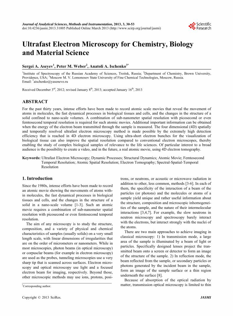
The transmission electron microscope (TEM) is the now the most common tool, designed to study very thin samples with thicknesses of about 10 - 100 nm at electron accelerating voltages of up to 200 kV [14]. Its scheme is similar to the optical system of an optical light microscope in that it creates an image of the sample based on the transmitted radiation beam. Figure 1 compares the main units of the transmission electron microscope to those of the optical microscope and the scanning electron micro- scope.
The transmission electron microscope consists of an electron gun and electromagnetic lenses. Figure 1 shows the path of the rays in a microscope with three levels of zoom and one condenser lens, which is used to pre-focus of the electron beam. The two common modes of its operation are the imaging mode and the recording of micro-diffraction patterns. In imaging mode, the plane of a sample conjugates to the screen, where it is assumed that the sample is very thin compared to the focal length of the imaging objective lens. In the diffraction mode, the object of observation conjugates to the back focal plane of the objective lens, where the distribution of the amplitudes of the electron beam, diffracted off the sample, corresponds to the Fraunhofer’s diffraction of the electrons. The resulting picture is observed on a remote screen. It is possible to determine the composition of the sample by analyzing the diffraction pattern [16].
In the phrase “micro-diffraction”, the word “micro” implies that the diffraction signal is observed only from a rather small area of the sample. The area is chosen either by a special selector diaphragm, installed in the plane of the first intermediate image (see Figure 1), or by irradia- tion of the desired part of the sample with a sharply- focused electron beam with a diameter of about 1 micrometer or less.
In imaging mode, the so-called aperture diaphragm is installed in the focal plane of the object lens in order to limit the aperture of the beam, i.e. the opening angle of the cone of rays emerging from the sample. This helps to decrease the spherical aberration, a basic imaging error associated with the projection of a point in the sample to a point of the image.
Modern microscopes are usually equipped with a two- lens condenser, which allows for a rather high electron
Copyright © 2013 SciRes. JASMI
Ultrafast Electron Microscopy for Chemistry, Biology and Material Science
Copyright © 2013 SciRes. JASMI
32
Electron gun
Magnetlenses
Sample
Sample
Sourceof light
Opticallenses
Opticalmicroscope
Detector
Lead glass
Phosphor screen
Transmission electron microscope
Raster electron microscope
Figure 1. Schematic of the optical, transmission and scanning electron microscopes [15].
flux to a small area of the object with characteristic size of 1 - 5 microns. This eliminates the growth of the films due to hydrocarbon polymerization of oil vapors as a result of electron bombardment of the unobserved sample areas in microscope where the column is pumped by diffusion pumps.
structure and composition of surfaces and near-surface layers, because the penetration depth of the electrons is very small.
3. Stroboscopic Electron Microscopy
Electron microscopy takes advantage of two of the three main properties of the electron: the small de-Broglie wavelength of the electron, which enables very high spa- tial resolution; and the electric charge, which allows to control its movement by electric and magnetic fields. About 60 years ago, the third property of the electron, its small mass (i.e., low inertia) began to be used in so- called stroboscopic electron microscopy for the study of periodic processes [17]. The essence of the method is quite simple: a sample with periodically time-varying characteristics, with a fixed rate of change, should be irradiated by short bunches of electrons with the same frequency and fixed phase. The synchronicity freezes the image, which corresponds to the state of the sample at the time of arrival of the electron pulses.
According to statistical data, tens of thousands of trans- mission microscopes with accelerating voltages of 80 - 100 kV have been produced. Hundreds of devices with an accelerating voltage of between 200 kV and 500 kV were created for the study of thicker objects, with a thickness of up to 10 microns. And there are only a few dozen microscopes intended for the voltage range from 1 MV to 3.5 MV.
For a typical transmission electron microscope with an accelerating voltage of 100 kV, the de Broglie wavelength of the electron is 3.7 pm. This is much smaller than the diameter of a hydrogen atom, which equals approximately 100 pm. This would seem to make it easy to observe any atomic particle, as long as the resolution of the electron microscope is on the order of the electron wavelength as is the case in optical microscopes. But in fact, it is extremely difficult to observe individual atoms because of the poor quality of the electron lenses compared to the light-optical lenses: at the same angular size of the light and electron beams, the electron lenses create almost of two orders of magnitude more aberrations and image distortion [13].
In the early 60’s, in the Soviet Union as a result of the work of Prof. G.V. Spivak, and in other countries, stro- boscopic techniques were developed for all major types of electron microscopes: translucent, raster, emission and mirror types [18,19]. These developments allowed the exploration of processes in rapidly varying thin films (transmission electron microscopy) and in the surface layers of solids (raster, emission and mirror microscope): re-polarization of various ferroelectrics; distinctions of the domain structure during re-magnetization of thin magnetic films; heterogeneity of alternating fields of
At a kinetic energy of 100 eV, the de Broglie wave- length of the electron is equal to 0.1 nm, i.e. on the order of atomic dimensions. Electrons with such energies are strongly diffracted by atomic lattices. This property is used in low-energy electron diffraction to investigate the

Ultrafast Electron Microscopy for Chemistry, Biology and Material Science 33
magnetic heads; and local defects of p-n junctions during their fast switching between the locked and open states [20]. Additionally, from a theoretical point of view, it is possible to study the microstructure of solution-gels in periodic reactions such as the Belousov-Zhabotinsky reaction using electrons with low kinetic energies, less than 100 eV, and to investigate the periodic sorption- desorption processes of catalysis in a similar fashion [20].
The initial work on stroboscopic microscopy was per- formed with micro- and nanosecond time resolution. Later, several laboratories started to investigate periodic processes with picosecond temporal resolution, usually using stroboscopic scanning electron microscopy. The main difficulties arose from the gating, the interruption, or the modulation of the electron beam. Generally, one uses one of two methods: first, it is possible to change of the intensity of the beam by locking or unlocking it with appropriate voltage pulses applied across the cathode or across the modulator in the electron gun of the micro- scope; or secondly, one can deflect a continuous electron beam by an electric or magnetic field in the vicinity of a skipping aperture of small diameter. The blanked, locked or unlocked electron pulses should be properly frequency and phase synchronized with the signals on the sample in order to avoid a loss of resolution.
The larger the duty cycle of the blanking pulses, i.e. the higher the ratio of the repetition period to the dura- tion of the front of the electron pulse, the better the tem- poral resolution of the stroboscopic microscope, but the lower the brightness of the image. Consequently, each application requires a careful assessment of the best trade-offs. Moreover, a very short front of the pulse causes the resolution of the microscope to deteriorate because of non-ideal edges of the pulse, the appearance of chromatic aberration in transmission electron micros- copy and the manifestation of the Bursch effect, which describes the transition of the longitudinal component of the electron velocity to a transverse component due to Coulomb repulsion.
4. Dynamic Transmission Electron Microscopy
Transmission electron microscopy, with its rather wide range of its tools, has long been a powerful technique in many fields of science and technology. While allowing to reach a spatial resolution on the sub-nanometer scale, conventional transmission electron microscopy does not permit an ultrashort temporal resolution, i.e. a time resolution in the picosecond or femtosecond regime. In contrast, optical microscopy using fluorescent probes, such as green fluorescent proteins, made it possible to visualize the processes occurring in vitro [2]. However,
despite the high temporal resolution of optical methods, their spatial resolution is usually limited by the wave- length to the range of 200 - 800 nm. A review article [21] and a recently published monograph [2] describe the development of the methods of 4D, dynamic tran- smission electron microscopy (DTEM) and ultrafast elec- tron microscopy (UEM), respectively.
The images and diffraction patterns in the work [22] were obtained at an accelerating voltage of 120 keV for non-organic materials (single crystals of gold, amorphous carbon and polycrystalline aluminum) and for biological cells of the intestine of rats [23]. In those studies, the gated beam contains on the average only one electron per pulse, with the total dose being limited to a few electrons per Å2. Note, that these electron pulses were completely controlled in space and in time. Conceptually, this works is based on the methods of time resolved electron dif- fraction (TRED) or ultrafast electron diffraction (UED) [1,24-26,78,112], ultrafast electron crystallography (UEC) [23] and the other DTEM studies [21], but with one important difference-namely, the implementation of synchronized pulses of single electrons to form an image. The sketch of this 4D DTEM is shown in Figure 2.
This single-electron approach differs quite remarkably from the one used in the work [27], which used single pulses with −108 electrons and pulse durations of −20 ns.
ElectrostaticBeam shifter
Hydro-drive laser
Cathode-drive laser
Laser-pulse-driven Photoelectron cathode
Sample location
CCD camera system
Figure 2. The schematic of a dynamic transmission electron microscope (DTEM) [21].
Copyright © 2013 SciRes. JASMI

Ultrafast Electron Microscopy for Chemistry, Biology and Material Science 34
Those pulses, used to study laser-induced melting of different metals, contain so many electrons that high temporal resolution is not possible. Moreover, as noted in [28], the uncertainty in the spatial resolution in these experiments due to statistical interferences was of the order of micrometers, because the temporal window for imaging was on a nanosecond scale. It was found, that the use of amplified femtosecond light pulses, with much higher intensity of about 12 210 W cm , led, at first, to the formation of an electron beam that was insensitive to the focusing system of the microscope, and, secondly, to a significant lengthening of the pulse, which was due to electron-electron Coulomb repulsion.
The single-electron per pulse approach of 4D UEM [22,29] was used to obtain images from polycrystalline and single crystals [2]. To verify the authenticity of the experiment, some images were collected when the fem- tosecond pump laser pulses were blocked. In this case, the pattern was not observed, confirming that the time resolved signal generated in the electron microscope was indeed induced optically, and that the contribution of thermal electrons that are continuously generated by the cathode can be neglected [29]. It is useful to remember that electron microscopes can operate in UEM and DTEM mode. To reach atomic scale spatial resolution, the UEM diffraction regime should be used by intro- ducing an intermediate lens to select the back focal plane of the lens as the object.
5. Controlling the Motions of Free Electrons by Femtosecond Light Pulses
Femtosecond lasers play a key role in 4D electron micro- scopy. Ultrashort pulses are necessary for the optical excitation of ultrafast processes in the sample and to form the ultrashort probe electron pulses. Additionally, pulsed laser radiation makes it possible to measure the temporal characteristics of the photoelectron bunches, to implement additional compression of electron pulses, and to generate electron bunches with durations that may potentially reach into the attosecond regime.
The last statements need to be amplified on, because they imply that is possible to control free electrons with a laser beam. At first glance, this statement conflicts with the well-known fact that free electrons cannot absorb the electromagnetic (EM) radiation because the laws of conservation of energy and momentum cannot simul- taneously be satisfied. Nevertheless, free electrons can scatter EM radiation. From a quantum mechanical point of view, this is the result of stimulated Compton scat- tering in a strong laser field.
The possibility to control the translational degrees of freedom of charged particles, in particular of free electrons, by a spatially inhomogeneous electromagnetic field was demonstrated theoretically by Gaponov and
Miller in the mid 1950’s [30]. This mechanism leads to the ejection of charged particles from the strong field. In the case of high-power laser radiation, the Gaponov- Miller, or ponderomotive (gradient) force (PF) [31], which is defined as the spatial gradient of the so-called ponderomotive potential Up, can reach sufficiently high values to form a basis for the effective control of electron pulses in vacuum.
For non-relativistic electrons, the concept of the pon- deromotive potential in a spatially inhomogeneous electromagnetic field sinoE E r t can be intro- duced by averaging the Hamiltonian H over the fast oscillations with frequencies and 2:
2
22 2
2
sin 2
2 4
2
o e
e o e
e p
H p eE r t m
p m eE r m
p m U
Here, me and e are the mass and the charge of the electron and denotes an averaging over optical cycles. As a result, the expression for the PF can be written as the following expression:
pond 2 2 2 30, 64π ,eF r t e m c I r t
Here 0 is the dielectric constant, c the speed of light and λ the wavelength of the laser radiation. It follows that for a tightly focused laser pulse with an intensity of
15 210 W cm in the center of a focal spot of 2 μm diameter (at the level of 1 e ) and λ=800nm, the force,
, is approximately equal to the strength of the interaction between two electrons separated by a distance of 5 nm. In this example, the ponderomotive potential is
pond 1110 NF
pU 60eV . It is evident that ultrashort laser radiation allows to
control free electrons in vacuum on a femtosecond scale. This makes possible both the creation of ultrashort photoelectron bunches and the measurement of their duration [32,33]. The determination of the temporal characteristics of a pulsed electron beam is based on scanning the time delay between the laser radiation that forms the photoelectric bunch and the tightly focused laser beam that changes the velocity distribution of the photoelectrons as a result of the PF. Such a method compares favorably with a standard streak camera in its final characteristics and can be used for femtosecond electron beams [33].
In a streak camera, the electrons are deflected by a high-speed and high-voltage electric field with an amplitude of about 2 - 5 kV before reaching a position- sensitive detector. The rate of change of the high electric field determines the temporal resolution of the device. The currently best time resolution is in the subpico- second range and reaches a value of −300 fs. In addition
Copyright © 2013 SciRes. JASMI
Ultrafast Electron Microscopy for Chemistry, Biology and Material Science 35
to this, it should be noted that the femtosecond temporal synchronization of the high-voltage electrical pulse in the streak camera and the femtosecond laser pulse that forms the ultrashort photoelectron bunch poses serious tech- nical challenges.
The study of the behavior of the free electrons in spatially inhomogeneous electromagnetic fields began shortly after the appearance of the theory of Gaponov and Miller and the first experiments were devoted mainly to the possibility of creating traps using microwave technology [34]. Here, special attention was focused on the observation of the passage of the electrons with a certain kinetic energy through the ponderomotive poten- tial, which allowed, for example, to determine the value of Up [34,35]. The first demonstration of scattering of the photoelectrons by the ponderomotive potential, created by an intense sub-nanosecond laser pulse, was done in the work [36]. Here the multi-photon ionization of Xe, especially bleeding in the vacuum system, was used to prepare the pulsed photoelectron beam with kinetic energies less than 5 eV. This experiment demonstrated the control of low-energy photoelectrons by an optical ponderomotive potential with the height of about 10 eV.
Special attention should be given to the measurement of the value of the PF with which tightly-focused femtosecond laser radiation acts on the electrons propa- gating in vacuum. This may be useful for in situ space- time diagnostics of the laser fields of high intensity, and can be used to validate the measurement of ultrashort electron pulse durations based on the irradiation of the electron bunches with the laser pulses of high intensity. Here it should be noted that the use of laser radiation with intensities of more than 14 210 W cm usually is accompanied by the photoionization of the residual gas in the vacuum system and thus by a possible deformation of the electron trajectories that pass through a cloud of charged particles.
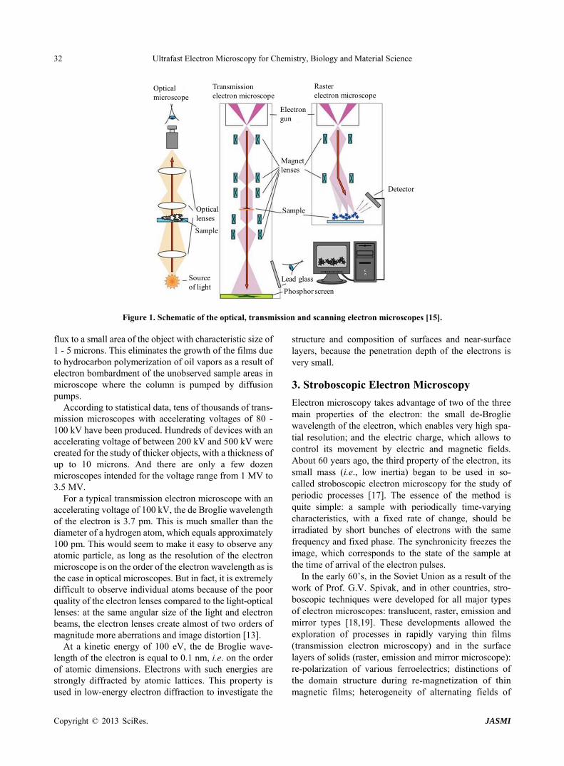
As was noted above, electrons are ejected from their field-free paths by a strong electromagnetic field. This is illustrated in Figure 3, which shows two counter- propagating tightly-focused laser beams forming a stand- ing wave from which the electron pulse is deflected. Such a scheme has a dual purpose. First, it allows to determine the duration of the initial electron bunch by scanning the timing of the laser pulses that create the standing wave, and using a position-sensitive scheme to detect the rejected, but in general, diffused, electron beam components. Secondly, the deflected electron pulses potentially have a shorter time duration compared to the incident electron pulses.
Two important remarks should be made here. The scheme in Figure 3 requires the spatial-temporal match- ing of two femtosecond laser pulses from two directions and a (sub)picosecond electron bunch from another di-
Figure 3. Deflection of an electron beam as a result of the optical ponderomotive force generated by an ultrashort laser pulse [2].
rection. The use of a single laser beam for the electron scattering would, of course, be simpler. However, in the standing wave the spatial inhomogeneity of the elec- tromagnetic field is about 2 , a rather small value that is technically difficult to obtain with a single amplified femtosecond laser beam. For example, a parabolic mirror can usually focus 0.8 - micron amplified femtosecond laser radiation to a spot diameter of 1 6ed microns. Therefore, for a given laser pulse energy, laser wavelength and focusing conditions, the scattering of electrons in a pulsed standing wave will be more pro- nounced.
Another important consideration relates to the ultimate possibilities of this approach. This is important because it is rather interesting to know the accuracy of the electron pulse duration measurement as well as the duration of the deflected electron bunch. These characteristics are directly related to the transit time of the fast electrons through the laser focal spot,
fin 1tr e ed v ,
where ve is the speed of the electron beam. Using
1 6ed μm and 810 m sev for electrons with kinetic energy of 30 keV, we find tr 60 fs . Note that the use of a standing wave formed by two laser beams (Figure 3) will not lead to a decrease in τfin, and hence the accuracy of measurement for this example will remain of the order of 100 fs. Therefore, to obtain a femtosecond electron bunch with 10 -50 fs and its full diagnostics it is important to ensure the tight focusing of intense laser radiation, and/or to use electrons with higher kinetic energy. Of course, in order to deflect these ultrafast electrons it is necessary to implement intense laser fields.
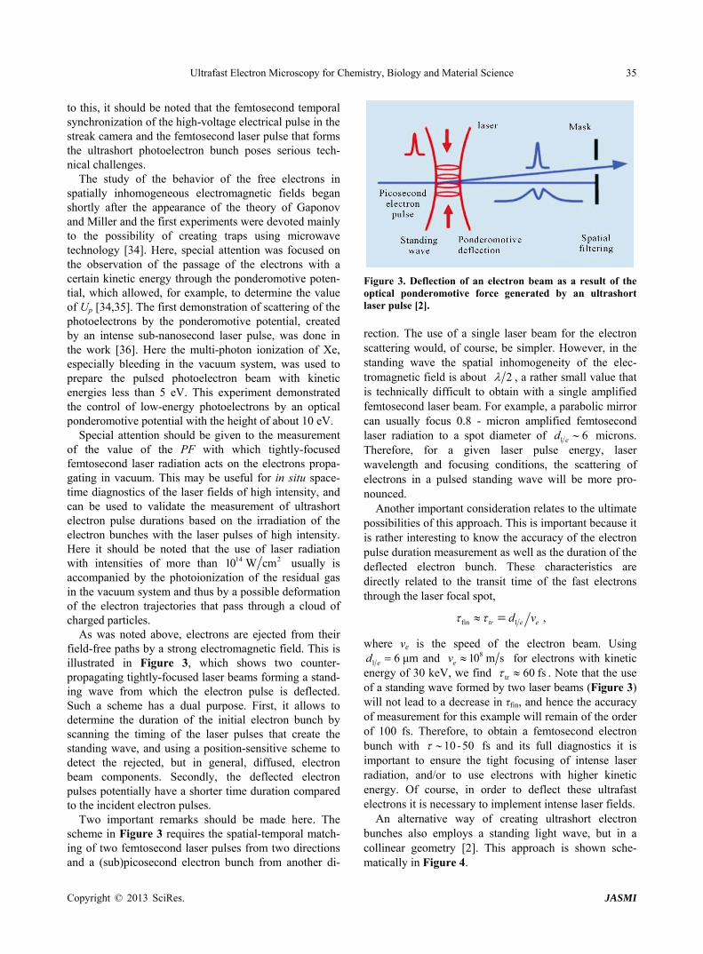
An alternative way of creating ultrashort electron bunches also employs a standing light wave, but in a collinear geometry [2]. This approach is shown sche- matically in Figure 4.
Copyright © 2013 SciRes. JASMI
Ultrafast Electron Microscopy for Chemistry, Biology and Material Science
Copyright © 2013 SciRes. JASMI
36
Figure 4. Schematic diagram of the creation of attosecond electron pulses. (a) An electron bunch with sub-picosecond dura- tion is irradiated by two counter-propagating laser beams (forward and after the bunch) with different wavelengths. In the reference frame of the electrons, the wavelengths are the same as a result of the Doppler effect, and a standing light wave is formed; (b) Ponderomotive forces push electrons away from the strong laser field; (c) As a result, the compression leads to the formation of electron bunches with attosecond duration. Strictly speaking, the envelope duration of the initial electron bunch remains constant, but importantly, the attosecond spikes appear inside the envelope [2].
In this context it should be recalled that on the basis of the uncertainty principle, , the existence of ultrashort, in this case attosecond, bursts needs a wide spectrum of energy Ee. For example, a bunch with 100 as (10−16 s) duration has at least . The initial picosecond photoelectron pulse does not exhibit such spectral properties. As shown in Figure 4, the required broadening is due to the work of the ponderomotive forces [2]. Let us illustrate this with a simple estimate, by writing down the expression for the work in the traditional sense, where the energy gain of the electrons is equal to p e
E t ħ
eE
v
6eV
pondeE F (τp-the laser pulse du-
ration), and the force is approximately defined as pond 2 pF U ( -wavelength of the laser radiation
in the reference frame of the fast electron). In the conditions of the numerical experiment [2] 0.2eV,pU
370nm, 810 m
problem. It is likely that it belongs to the class of experiments in which it is easier to create an ultrashort bunch than to measure it.
6. Ultrafast Electron Microscopy
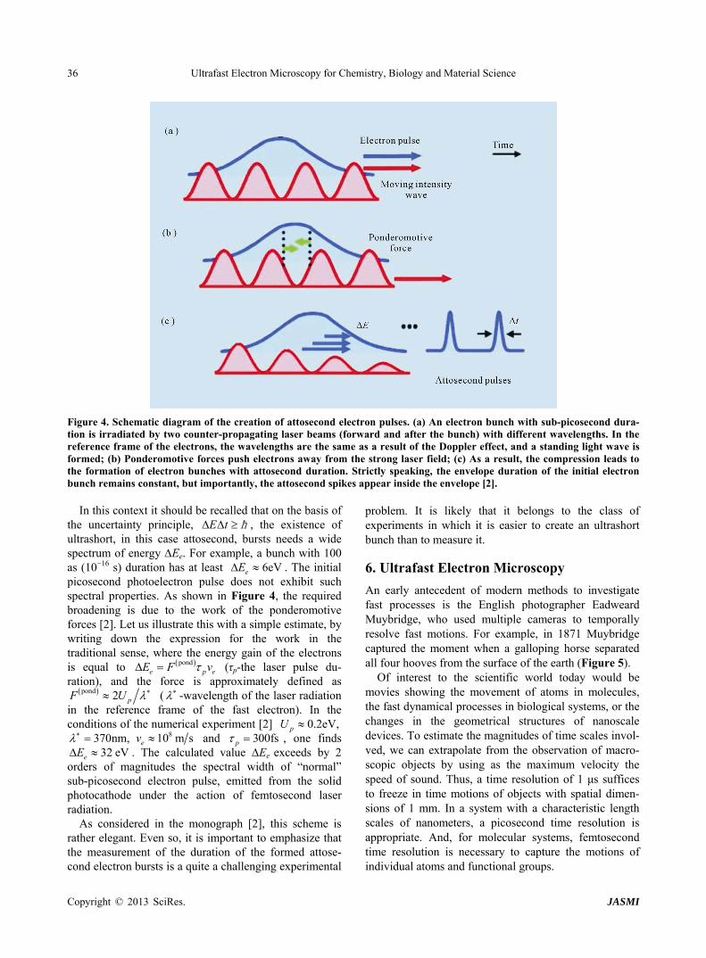
An early antecedent of modern methods to investigate fast processes is the English photographer Eadweard Muybridge, who used multiple cameras to temporally resolve fast motions. For example, in 1871 Muybridge captured the moment when a galloping horse separated all four hooves from the surface of the earth (Figure 5).
Of interest to the scientific world today would be movies showing the movement of atoms in molecules, the fast dynamical processes in biological systems, or the changes in the geometrical structures of nanoscale devices. To estimate the magnitudes of time scales invol- ved, we can extrapolate from the observation of macro- scopic objects by using as the maximum velocity the speed of sound. Thus, a time resolution of 1 μs suffices to freeze in time motions of objects with spatial dimen- sions of 1 mm. In a system with a characteristic length scales of nanometers, a picosecond time resolution is appropriate. And, for molecular systems, femtosecond time resolution is necessary to capture the motions of individual atoms and functional groups.
se and v 300fsp , one finds . The calculated value Ee exceeds by 2
orders of magnitudes the spectral width of “normal” sub-picosecond electron pulse, emitted from the solid photocathode under the action of femtosecond laser radiation.
32 eVeE
As considered in the monograph [2], this scheme is rather elegant. Even so, it is important to emphasize that the measurement of the duration of the formed attose- cond electron bursts is a quite a challenging experimental

Ultrafast Electron Microscopy for Chemistry, Biology and Material Science 37
Figure 5. One of the first movies in history. These images were obtained by E. Muybridge in 1871. The time delay between the exposures was about 50 ms [37].
The ultrafast electron microscope built at the Cali- fornia Institute of Technology [2] is designed to explore a class of problems that occur on picosecond or sub- picosecond time scales. A schematic illustration of this instrument is shown in Figure 6.
It is convenient to conceptualize the setup as con- sisting of three main sections: 1) the formation and acceleration of the sub-picosecond pulsed electron beam; 2) the interaction unit, in which the sample is excited by femtosecond laser pulses and its spatial-temporal stru- cture probed by ultrashort electron bunches; and 3) the position-sensitive detection of the electrons after their interaction with the sample. The use of electron beams of subpicosecond duration imposes strict requirements on the detector, because the probe pulse cannot contain a large number of electrons. As it will be illustrated below, the main cause of the electron pulse temporal spreading is the space-charge interaction between the electrons within each pulse on account of their Coulomb repulsion. Therefore, the detection efficiency for electrons in this microscope should be as high as possible. Much prepa- ratory work was done to achieve this [2]. As a result, the detection efficiency for the time-resolved instrument is almost an order of magnitude higher than that of a standard electron microscope. This also provides an interesting opportunity to significantly reduce the expo- sure (the total number of electrons passing through the sample to form an image on the detector), which is particularly important for imaging biological samples that are very sensitive to radiation induced damage.
Figure 6. Schematic illustration of an ultrafast electron microscope. A commercial electron microscope, operating in a continuous mode, can be taken as a basis in order to create such a device. To adapt it to 4D microscopy requires a femtosecond laser, which provides a pulsed excitation of the sample (corresponding to a laser beam shown in red), and allowing for the preparation of the photoelectron probe pulse of ultrashort duration (ray marked in blue) [2].
Copyright © 2013 SciRes. JASMI

Ultrafast Electron Microscopy for Chemistry, Biology and Material Science 38
The ultrashort electron bunch is the essence of 4D electron microscopy. Therefore, the question of its dura- tion should be given special attention. The duration of the photoemission of electrons from the surface of a solid cathode and therefore the initial duration of the photo- electron bunch are determined by the duration of the laser pulse. But during the propagation from the photo- cathode to the target, the electron beam is stretched in time. Here we consider three major factors that lead to a smearing of the electron bunch.
First, the acceleration of photoelectrons in a static electric field near the cathode causes so-called time-of- flight chromatic aberration for the electrons (TFCA). The temporal resolution limit is given by:
2EF e em E eF ,
where Ee is the initial spread of the kinetic energy of the electrons as they emerge from the cathode and F is the electric field in the acceleration gap.
The expression for TFCA can be obtained by solving a quadratic equation that describes the uniformly accelerated motion of the electrons in the acceleration gap of the length of l:
20 2ev t eF m t l
Differentiating the both sides of the equation with respect to time t, we get:
0 0ev eF m t
from which immediately follows the expression for TFCA. Let us consider a numerical example. At Ee = 0.3 eV and 810 V mF , which approximately corres- ponds to the maximum value of the field (higher values lead to vacuum breakdown even with special electrodes that underwent thorough mechanical, electronic and ionic treatment), this contribution is 60 fsEFt .
Secondly, the movement of electrons through the field free flight tube with slightly different kinetic energies is accompanied by an elongation of the time of flight, which is expressed as
2TOF TOF et E K
Here, tTOF is the time of flight of the electrons with kinetic energy K from the photocathode to the sample. At
and , correspond- ing to the length of 30 cm between the cathode and the target, we get .
30 keV, 0.3 eVeK E
15 fsTOFt
3 nsTOFt
Thirdly, the Coulomb repulsion between the electrons within a pulse causes a swelling of the photoelectron bunch. To assess the effect of this mechanism on the temporal properties of the beam, we consider a simple model, in which the electron bunch is travelling through a field-free region. (Here the field-free region is taken for
the simplicity.) The total energy of the bunch, consisting of N electrons, is conserved:
2 201 2 4π 1 2i j e iV W e m v r r
Therefore, the characteristic value of the distribution of the velocities, v, resulting from the electrons pushing apart each other can be qualitatively estimated by using the expression
2 202 16πem v e N r ,
where r is the initial size of the photoelectron cloud. In this model, the velocity spread of the electrons causes the elongation of the order of C TOF et v v , which can be rewritten as:
208πC TOF e et v e N rm
At 8 410 m s , 10 , 3 nse TOF and v N t 10 mmr , corresponding to the size of the focal spot
of the tightly focused laser beam, this contribution in the framework of the simple model is equal to 5 psC . This shows that the Coulomb repulsion of the electrons in the electron bunch is the main factor limiting the ability of ultrafast electron microscopy. Naturally, the use of ultra-high accelerating voltages, such as 500 kV instead of 30 kV, can reduce the swelling of the electron bunch due to Coulomb repulsion, but can also lead to destruction of the sample. Use of very fast electrons, in the MeV range, can further reduce the space-charge broadening because of the onset of relativistic effects [110,111]. It should also be noted that a system based on a TOF electro-static mirror, a so-called reflectron, can be used to re-compress the electron bunches after their original spreading [26,38]. At the present time, a radio frequency compression scheme is already in use for this purpose.
A serious challenges in the field of 4D electron micro- scopy remains the task of observing an image or a diffraction pattern produced by a single, ultrashort elec- tron pulse. The solution to this problem is rather impor- tant, because it would enable the study of ultrafast irre- versible processes. An early breadkthrough has been achieved by a collaboration of scientists at Brown Uni- versity and at SLAC, who used ultrashort electron pulses with 5.4 MeV of energy, generated using the Gun Test Facility at SLAC, to record single-shot diffraction patterns of 160 nm thick aluminum foils [110,111]. Their work showed that MeV electrons should make it possible to achieve sub-100 fs time resolution. Subsequently, phy- sicists in Japan were able to collect diffraction patterns of thin gold films with single subpicosecond electron bunches [39]. They applied a magnetic sector in order to compress the electron beam in the experiment [39].
Copyright © 2013 SciRes. JASMI

Ultrafast Electron Microscopy for Chemistry, Biology and Material Science
Copyright © 2013 SciRes. JASMI
39
Non-Thermal vs Thermal Melting of a Solid Irradiated by a Femtosecond Laser
experiment. The results are shown in Figure 7. Figure 7 clearly demonstrates, that the lattice is heated
and remains in the solid phase with a distinct diffraction pattern on a time scale of up to 1.5 - 2.5 ps after the excitation by laser pulse, which is consistent with the thermal melting. Current research continues in this direc- tion.
The study of ultrafast phase transitions in condensed matter is one of the most interesting fields of 4D electron microscopy, viz. ultrafast electron crystallography. To induce an ultrafast phase transition such as the melting of a solid, it is necessary to insert energy into the lattice within a small period of time and to reach the critical temperature as quickly as possible. The most suitable tool to accomplish this is a femtosecond laser pulse. In metals and semiconductors, the photons excite the electrons (and the holes) to high-lying electronic states, resulting in a change of the charge density. Initially, the absorbed energy is stored in electronic degrees of freedom. With the decrease of electron density between the atoms, the bonds in the system become weaker, and at some degree of excitation, the lattice is no longer fixed. Such processes may lead to non-thermal melting of a solid, provided that they are fast compared to the relaxa- tion of the electron energy into the lattice vibrations (phonons). Preliminary studies of aluminum by a femto- second laser pump-probe have shown that in this material, the transition from a solid to a liquid phase occurs within 500 fs, i.e. faster than the energy transfer from the exci- ted electrons to the phonons [40].
7. Phase Transitions in Nanoparticles
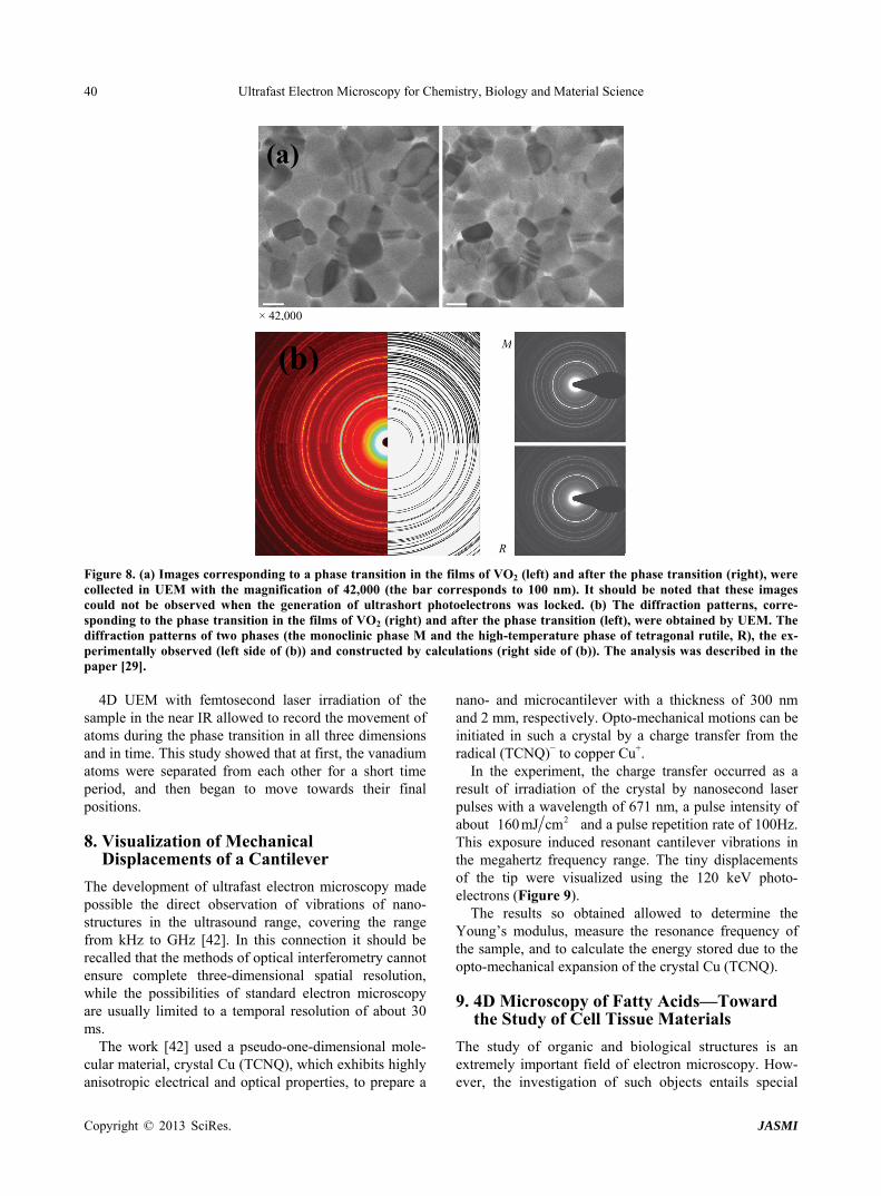
Vanadium dioxide, VO2, undergoes a phase transition of the first type from a low-temperature monoclinic phase (M) into a high-temperature tetragonal phase of rutile (R) at −67˚C. This phase transition has been the subject of intensive research since its discovery almost half a century ago. The work [29] describes the first study of this material using 4D UEM. Because single electron probe pulses were used, Coulomb (space-charge) repul- sion was absent. The experiment demonstrated the possi- bility of obtaining a sequence of images (i.e. a movie) with atomic-scale spatial resolution combined with an ultrashort temporal resolution. In particular, it was shown that it was possible to investigate the ultrafast metal- insulator phase transitions in vanadium dioxide. A struc- tural phase transition in VO2 nanoparticles is exhibited in the diffraction patterns (at atomic scale) and UEM images (at nanometer scale) with a characteristic hystere- sis with a temporal resolution on the order of 100 fs (Figure 8).
The direct observation of melting of Al with subpico- second temporal resolution has been achieved by ultra- fast electron diffraction [41]. A 20 nm thick film of polycrystalline aluminum was used as the sample in this
Figure 7. Electron diffraction patterns from a film of polycrystalline Al, recorded at different times after the excitation by a femtosecond laser pulse as labelled. The energy density of the laser pulse is about 70 mJ/cm2 [41].
Ultrafast Electron Microscopy for Chemistry, Biology and Material Science 40
(a)
× 42,000
(b)
R
M
Figure 8. (a) Images corresponding to a phase transition in the films of VO2 (left) and after the phase transition (right), were collected in UEM with the magnification of 42,000 (the bar corresponds to 100 nm). It should be noted that these images could not be observed when the generation of ultrashort photoelectrons was locked. (b) The diffraction patterns, corre-sponding to the phase transition in the films of VO2 (right) and after the phase transition (left), were obtained by UEM. The diffraction patterns of two phases (the monoclinic phase M and the high-temperature phase of tetragonal rutile, R), the ex-perimentally observed (left side of (b)) and constructed by calculations (right side of (b)). The analysis was described in the paper [29].
4D UEM with femtosecond laser irradiation of the
sample in the near IR allowed to record the movement of atoms during the phase transition in all three dimensions and in time. This study showed that at first, the vanadium atoms were separated from each other for a short time period, and then began to move towards their final positions.
8. Visualization of Mechanical Displacements of a Cantilever
The development of ultrafast electron microscopy made possible the direct observation of vibrations of nano- structures in the ultrasound range, covering the range from kHz to GHz [42]. In this connection it should be recalled that the methods of optical interferometry cannot ensure complete three-dimensional spatial resolution, while the possibilities of standard electron microscopy are usually limited to a temporal resolution of about 30 ms.
The work [42] used a pseudo-one-dimensional mole- cular material, crystal Cu (TCNQ), which exhibits highly anisotropic electrical and optical properties, to prepare a
nano- and microcantilever with a thickness of 300 nm and 2 mm, respectively. Opto-mechanical motions can be initiated in such a crystal by a charge transfer from the radical (TCNQ)− to copper Cu+.
In the experiment, the charge transfer occurred as a result of irradiation of the crystal by nanosecond laser pulses with a wavelength of 671 nm, a pulse intensity of about 2160 mJ cm and a pulse repetition rate of 100Hz. This exposure induced resonant cantilever vibrations in the megahertz frequency range. The tiny displacements of the tip were visualized using the 120 keV photo- electrons (Figure 9).
The results so obtained allowed to determine the Young’s modulus, measure the resonance frequency of the sample, and to calculate the energy stored due to the opto-mechanical expansion of the crystal Cu (TCNQ).
9. 4D Microscopy of Fatty Acids—Toward the Study of Cell Tissue Materials
The study of organic and biological structures is an extremely important field of electron microscopy. How- ever, the investigation of such objects entails special
Copyright © 2013 SciRes. JASMI

Ultrafast Electron Microscopy for Chemistry, Biology and Material Science 41
Figure 9. 4D electron micrographs of a nanoscale cantilever. The frames show difference images, i.e. time dependent images where a reference frame is subtracted out. The image recorded at negative delay (−10 ns) relative to the 671 nm pump laser pulse served as a reference frame. A scale bar in the lower left corner corresponds to 200 nm [42]. demands on the microscope. This is primarily due to the increased sensitivity of the bio-structures to possible irreversible deformation and damage that can be caused by a beam of fast electrons. Therefore, for successful experiments in this field it is necessary to ensure an extremely high detection efficiency of the electrons passing through the sample. Note that the efficiency of the detector is directly related to the time of exposure. In this connection it is helpful that the high detection efficiency in the 4D microscopy allows working with a smaller number of electrons in the bunch.
Amongst the most common biological structures are membrane-type layers of fatty acids. In the laboratory, two-dimensional crystals can be created from long fatty acid hydrocarbon chains. It is possible to use the Langmuir-Blodgett technique to prepare the monomo- lecular layers of organic material on a solid substrate. It is rather interesting to observe the transition from a two-dimensional to a three-dimensional crystal of the long molecular chains and to visualize the self-assembly processes.
C20H42 chains with a length of 95Å on a silicon substrate were considered in computer simulations [2]. In the model, an ultrafast pulsed heating of the substrate leads to further changes in the inter-atomic distances of C20H42, reflecting the coherent motion of the atoms in the molecular chain. Each step of the calculation corresponds to a time interval of 0.5 fs, while the total number of steps reaches 200,000. Model calculations have shown an increase in the length of the fragment -CH2-CH2-CH2- that is located in the immediate vicinity of the silicon surface, by about −0.08 Å during 5 ps.
The 4D UEM method should allow us to study more complex biological samples that are directly related to the life sciences. It should be recalled that the use of ultra-short electron bunches for the visualization of biological tissues can improve the spatial resolution of the device compared to conventional electron micros- copy. In some ways the situation is similar to making a snapshot by a photographic camera with a long exposure time: the resulting image becomes quite fuzzy (Figure 10), but admittedly, can lead to a new artistic perception of reality.
The 4D electron microscopy succeeded in imaging stained cellular material in rat tissue (Figure 11), and of crystalline proteins, or cells in the vitreous bodies.
10. Musical Nanoscale Instruments: from the Drum to the Harp and the Piano
Ultrathin plates of graphite, gold, or other material, sub- jected to pulsed laser heating, can experience an ultrafast deformation (bending) as a result of anisotropic expan- sion of the atomic structure. As it turned out, the vibra- tions that accompany such deformations may be surpri- singly interesting.
Electron bunches at 200 keV were used to visualize mechanical vibrations of graphite nano-sheets (the mem- branes) with thicknesses of 75 nm. Vibrations with sub- millisecond temporal intervals resulted from exposure to pulsed laser radiation with a wavelength of 532 nm and a repetition rate of 5 kHz [2]. The energy density of the focused laser pulses reached a value of about 7 mJ/cm2.
Immediately following the pulsed laser heating of the
Copyright © 2013 SciRes. JASMI

Ultrafast Electron Microscopy for Chemistry, Biology and Material Science 42
Figure 10. Photograph of a city at night, made with a long exposure time. (The figure is carried over from [43]).
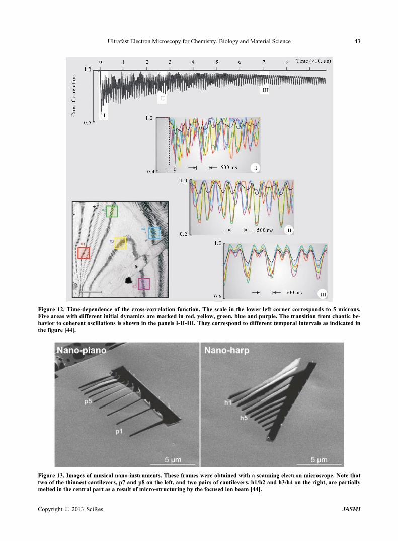
Figure 11. Images of stained cells of rat-related tract, ob- tained using ultrafast electron microscopy. The micrograph shows the micro-villas in the intestinal epithelium of new- born rats and numerous small vesicles (blisters) in the cyto- plasm. An enlarged image of the vesicles, pointed by the arrow on the left frame, is given on the right [2]. membrane, individual carbon atoms were found to vibrate in a random order. But after a few tens of micro- seconds, the corresponding modes of the membrane began to be synchronized (Figure 12), resembling a “drumbeat” with a frequency of around 1 MHz.
The processing of the images (Figure 12) used a cross-correlation function defined as
2
, , , , , , ,
;
x y x y x y x y x y x y x y
t t
C t C t C t S C t
2
where the contrast is
, ,x y x yC t N t N t N t .
Here, is the number of counts corresponding to
the picture element (pixel) with the coordinates of
,x yN t
,x y , and N t is the average number of the counts. 2000 images, collected with an interval of 50 ns, were used in Figure 12. The micrograph of the graphite mem- brane is represented in the lower left corner.
The success with the graphite nano-sheets inspired the search for other musical nano-instruments. A harp and a piano, constructed at the nanoscale, were made using arrays of cantilevers (Figure 13). They were prepared by micro-structuring of multilayer workpieces of
3 4Ni Ti Si N using sharply-focused ion beams [44]. The workpieces consisted of 30 nm layers of nickel and titanium, consistently applied to 15 nm film of Si3N4. For the piano, the cantilevers had almost the same lengths, approximately 4.6 μm, but their width varied from about 400 nm to 2.3 μm. In the harp, the lengths and widths of individual elements varied in the range of 1.2 - 9.1 μm and −300 - 600 nm, respectively.
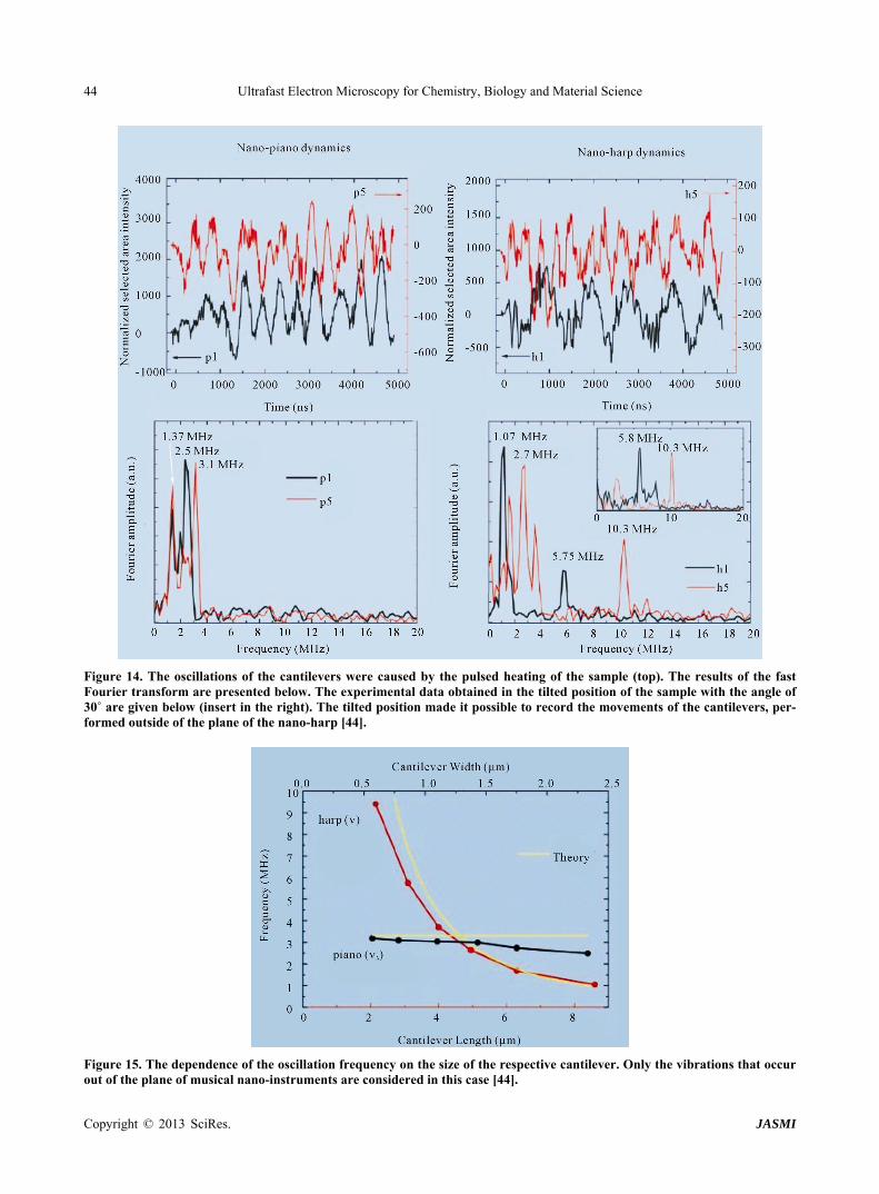
In the experiment, a sample (the harp or the piano) was heated by nanosecond 519 nm (or 532 nm) pulses from a Nd:YAG laser with a pulse repetition rate of 1 kHz. The energy density per pulse reached 2 mJ/cm2. As a result of the heating of the sample, consisting of the layers with different coefficients of thermal expansion, the me- chanical deformation of the cantilever triggered its vibra- tions. The mechanical movements were observed using the photoelectrons that were obtained by illuminating the photocathode with the fourth harmonic of a Nd:YAG laser. The results for individual cantilevers p1, p5, h1 and h5 (for convenience they are shown in Figure 13) are presented in Figure 14. The combined results of the observations are given in Figure 15.
In the next series of the experiments, the femtosecond laser with MHz pulse repetition rate was used “to play an instrument.” Here a fiber laser generator with pulse repetition frequency of about 25 MHz was used. The en- ergy density per pulse was in the range of 20 - 30 mJ/cm2.
Beyond their academic interest, the musical nano- systems can have very specific applications. For example, the authors [44] note that such layered nanostructures can be used to precisely measure the temperature of a device with a spatial resolution of 10 μm in combination with a microsecond temporal resolution.
11. 4D Electron Tomography
Electron tomography began to develop as early as the 1960-ies [45]. Progress in this field was mainly limited by the development of computers, because it is important to process a large number of 2-dimensional electron dif- fraction patterns and combine them in a single movie. A humorous illustration to these words is given in two images of (Figure 16), taken from the book [45].
The use of modern laser technology has allowed to add to electron tomography the fourth dimension, time, and thus to create a completely unique device (Figure 17).
Copyright © 2013 SciRes. JASMI
Ultrafast Electron Microscopy for Chemistry, Biology and Material Science
Copyright © 2013 SciRes. JASMI
43
Figure 12. Time-dependence of the cross-correlation function. The scale in the lower left corner corresponds to 5 microns. Five areas with different initial dynamics are marked in red, yellow, green, blue and purple. The transition from chaotic be-havior to coherent oscillations is shown in the panels I-II-III. They correspond to different temporal intervals as indicated in the figure [44].
Figure 13. Images of musical nano-instruments. These frames were obtained with a scanning electron microscope. Note that two of the thinnest cantilevers, p7 and p8 on the left, and two pairs of cantilevers, h1/h2 and h3/h4 on the right, are partially melted in the central part as a result of micro-structuring by the focused ion beam [44].
Ultrafast Electron Microscopy for Chemistry, Biology and Material Science 44
Figure 14. The oscillations of the cantilevers were caused by the pulsed heating of the sample (top). The results of the fast Fourier transform are presented below. The experimental data obtained in the tilted position of the sample with the angle of 30˚ are given below (insert in the right). The tilted position made it possible to record the movements of the cantilevers, per-formed outside of the plane of the nano-harp [44].
Figure 15. The dependence of the oscillation frequency on the size of the respective cantilever. Only the vibrations that occur out of the plane of musical nano-instruments are considered in this case [44].
Copyright © 2013 SciRes. JASMI

Ultrafast Electron Microscopy for Chemistry, Biology and Material Science
Copyright © 2013 SciRes. JASMI
45
Figure 16. The humorous evolution of 3D tomography [45].
(a) (b)
Figure 17. (a) Schematic diagram of 4D electron tomography. (b) A series of two-dimensional electronic images taken at dif- ferent angles and time delays. In [46] the angle range from −58˚ to +58˚ with increments of 1˚. The total number of projec- tions reaches 4000 [46].
The temporal behavior of carbon nanotubes was stu-
died by 4D tomography in the work [46]. The sample was twisted in the form of a bracelet. The measured length of the nanotube was L ≈ 4.4 microns. The images in Figures 18 and 19 were obtained using the 200 keV electron pulses. Femtosecond laser excitation led to the heating of the nanotube and caused the subsequent structural changes that began on a picosecond temporal scale.
nanotube, because the total dose received by the carbon sample during the experiment was about 2 orders of magnitude less than the value at which the irreversible deformation occurs. This is a tribute to the extremely high detection efficiency reached in 4D electron microscopy.
12. Electron Microscopy with High Spectral, Spatial and Temporal Resolution
The combination of spatial nano-resolution and subpico- second, eventually femtosecond temporal resolution, forms the basis of the atomic movie. Naturally, when the energy of the electron beam, transmitted through the sample, is measured in a sim lar geometry, additional and
Of particular interest to a broad audience is that it is possible to create a video, and in the future, a real atomic movie, using the results of 4D electron tomography. It should be emphasized that the pioneering experiment [46] did not induce irreversible changes in the structure of the i

Ultrafast Electron Microscopy for Chemistry, Biology and Material Science 46
Figure 18. (a) 3D images of multi-walled carbon nanotubes at different times. The lengths of the respective segments around a fixed area are denoted as L1 and L2; (b) Cross section of the 3D images. Two-dimensional slices in the plane xy are shown. Slice thickness is 4.6 nm. Dark areas of the arrows point to the nanometer-thick walls. According to these micrographs, the spatial resolution of the method is sufficient for the correct imaging of channels with a diameter of −10 nm; (c) An image, taken with a transmission electron microscope [46].
Figure 19. Mechanical vibrations of a carbon bracelet. The arrows indicate the direction of the individual sections of a carbon nanotube [46].
very important information is obtained. Note that for most modern research laboratories, such a study would pose quite a serious experimental challenge. Therefore, the precedent in this field plays an important role.
This idea was realized in the work [47] using a single metal nanostructure. In this experiment, the silver particle of triangular shape with a characteristic length of 130 nm and thickness of 20 nm, placed on a substrate of graphene (Figure 20), was irradiated by femtosecond laser pulses with a photon energy of 2.4 eV. The plasma oscillations in silver, excited by the optical radiation, were probed by an ultrashort electron beam with a diameter of 10 nm. The electron beam could be moved over the surface of the sample. Here the energy gain of the electrons, passed through the sample, was measured in addition to the spatial and temporal characteristics.
It is important to emphasize that due to the field localized on the surface of a metal particle, the electrons can not only lose kinetic energy, as would be the case with a standard transmission electron microscope, but also to acquire energy (Figure 21). In principle, this process can be controlled by changing the wavelength of the laser radiation. The accuracy of this procedure is determined by the spectral width of the laser pulse and could reach values of about 1 meV.
Copyright © 2013 SciRes. JASMI

Ultrafast Electron Microscopy for Chemistry, Biology and Material Science 47
Figure 20. The process of ultrafast spectral imaging. A 10-nm electron beam was scanned over the silver particle that was previously excited by a femtosecond laser pulse. For each position of the probe, the change of the kinetic energy of the elec- trons (viz. electron spectrum) was measured as a function of the delay between the exciting, optical, and probing, electronic, pulses. The increase in the energy of the electrons is measured in units of the photon energy, being equal to h = 2.4 eV [47].
Figure 21. Spectral and temporal characteristics of silver nanoparticles. The electron spectrum, obtained at a delay of 100 fs after the femtosecond optical pulse, is shown below. It is schematically indicated by the position of the electron nanobeam with respect to the triangular silver particle, which is depicted in gray [47].
The results of the measurement of the plasmic texture, generated on the surface of the silver particle, is shown in Figure 22.
It is clearly seen in Figure 22 that the field of plasma oscillations, excited by the laser radiation, is concentrated near the vertices (the cusps) of the triangular particle. There is a fairly good agreement with theory. Qualita- tively similar results were obtained near the sharp edge of a copper surface irradiated by the laser [47].
13. Conclusions
Electron microscopy and diffraction with a high temporal resolution have opened the possibility of directly observ- ing processes that occur in non-steady states of the studied substances. A temporal resolution on the order of 100 fs
corresponds to the transition of a quantum system through an energy barrier of a potential surface, describing a chemical reaction in the processes of breaking and forming new bonds of the interacting agents. The advan- ces thus opened the possibility of investigating the coherent nuclear dynamics of molecular systems and condensed matter [24,25,48-51].
In the past two decades it has been possible to observe the motions of nuclei in time intervals corresponding to the period of the oscillation of the nuclei. The observed coherent changes in the nuclear system at such time steps determine the fundamental transition from the standard kinetics to the dynamics of the phase trajectory of a single molecule, the molecular quantum state tomography [50- 53].
Copyright © 2013 SciRes. JASMI

Ultrafast Electron Microscopy for Chemistry, Biology and Material Science 48
Figure 22. Plasma oscillations, optically excited in the silver nanostructure, were visualized by a 10 - nm electron beam. Here, the electron signal is proportional to the height of the corresponding cylinder. For each panel, the energy, acquired as a result of the interaction of the electrons with nanolocalized fields, is shown in the lower right corner [47].
Figure 23. Chronology of the basic works (the first steps) in Dynamic Electron Microscopy, done in the first two decades (1982-2004) [21]. The parallel development of UED, UEM, UEC and DTEM until 2010 is described in [2]. The references 58 109] demonstrate the worldwide experimental activity in this field. [ -
Copyright © 2013 SciRes. JASMI
Ultrafast Electron Microscopy for Chemistry, Biology and Material Science 49
At the present time, the method of ultrafast diffraction
continues its rapid development. The methods of ultrafast electron crystallography and electron microscopy with temporal resolution from micro- to subpicoseconds provide great opportunities to the study of the 4D structural dynamics (see the review articles [21,54] and the mono- graph [2]). Very recent advances in the formation of ultra- short electron pulses allow us to reach an attosecond tem- poral resolution and observe the coherent dynamics of the electrons in molecules [55-57].
The development of dynamic electron microscopy and the first steps devoted to the progress in the study of structural dynamics of ultrafast processes are illustrated in Figure 23. It is all but certain that exciting developments in this field will continue into the future.
14. Acknowledgements
Academician of the RAS, Prof. A. L. Buchachenko, Prof. E. A. Ryabov, Prof. V. N. Bagratashvili, Dr. A. E. Luk’yanov, A. A. Timofeev, Prof. V. R. Flid, and Dr. James Beckman (Therapon, Inc.) are acknowledged for the hepful discussions. This work was supported by grants: No. 2012-1.1-12-000-1009-055 (from the Ministry of Education and Science of the Russian Federation) and No. 10-02-92000-ННС_а, 11-02-00868-а, 12-02-00840-a (from the Russian Fund for Basic Research). PMW ac- knowledges support by the Division of Chemical Sci- ences, Geosciences, and Biosciences, the Office of Basic Energy Sciences, the U.S. Department of Energy, Grant No. DE-FG02-03ER15452.
REFERENCES [1] A. A. Ischenko, V. V. Golubkov, V. P. Spiridonov, A. V.
Zgurskii, A. S. Akhmanov, M. G. Vabishevich and V. N. Bagratashvili, “A Stroboscopical Gas-Electron Diffraction Method for the Investigation of Short-Lived Molecular Species,” Applied Physics B, Vol. 32, No. 3, 1983, pp. 161-163. doi:10.1007/BF00688823
[2] A. H. Zewail and J. M. Thomas, “4D Electron Micros- copy. Imaging in Space and Time,” Imperial College Press, London, 2010.
[3] B. K. Weinstein, “Atomic Resolution Electron Micros- copy,” Soviet Physics Uspekhi, Vol. 152, No. 3, 1987, pp. 75- 122. doi:10.3367/UFNr.0152.198705c.0075
[4] J. Brandon and W. Kaplan, “Microstructure of Materials. Methods of Research and Monitoring,” M. Technosphere, Bergenfield, 2004.
[5] A. Vlasov, K. A. Yelsukov and V. Panfilov, “Microscopy Techniques,” Publishing House of Moscow State Tech- nical University named after Bauman, Moscow, 2011.
[6] A. Vlasov, K. A. Yelsukov and I. A. Kosolapov, “Elec- tron Microscopy,” M. Bauman Bauman, Moscow, 2011.
[7] D. Shindo and T. Oikawa, “Analytical Transmission Electron Microscopy for Materials Science,” M.: Mir,
Moscow, 2006.
[8] Y. S. Umansky, J. N. Skakov, A. N. Ivanov and L. N. Rastorguev, “Crystallography, X-Ray and Electron Mi- croscopy,” Metallurgy, Moscow, 1982.
[9] R. Kheidenraikh, “Fundamentals of Transmission Elec- tron Microscopy,” Academic Press, Waltham, 1966.
[10] P. Hirsch, A. Howie, R. Nicholson, D. Pashley and M. Whelan, “Electron Microscopy of Thin Crystals,” World, Moscow, 1968.
[11] M. V. Locquim and M. Langeron, “Handbook of Mi- croscopy,” Butterworths, London, 1983.
[12] J. Spence, “Experimental Electron Microscopy Razresh- eniya,” M.: Science, Poole, 1986.
[13] I. Watt, “The Principles and Practice of Electron Micros- copy,” Cambridge University Press, Cambridge, 1985.
[14] G. Thomas and M. J. Gorindzh, “Transmission Electron Microscopy of Materials,” Nauka, Moscow, 1983.
[15] E.A. Gudilin, “Electron Microscopy,” 2008. http://www.nanometer.ru/2008/12/21/electron_microscopy_55002.html
[16] C. Amelinks, “Methods of Direct Observation of Disloca- tions,” Wiley, Hoboken, 1968.
[17] M. Motosuke, S. Tetsuya, “Stroboscopic Scanning Elec- tron Microscope,” US Patent Number: 4538065, 1985.
[18] G. V. Spivak, V. V. Shakmanov, V. I. Petrov, A. E. Lukyanov and S. Yakunin, “On the Application of the Gates with the Deflection Plates in a Stroboscopic Elec-tron Microscopy,” Mathematical USSR Physics Series, Vol. 32, No. 7, 1968, pp. 1111-1114.
[19] A. E. Lukyanov, V. Galstyan and G. V. Spivak, “About Stroboscopic Scanning Electron Microscopy Four-Semi- conductor Structures,” Technology and Electronics, No. 11, 1970, pp. 2424-2427.
[20] M. L. Taheri, N. D. Browning and J. Lewellen, “Sympo- sium on Ultrafast Electron Microscopy and Ultrafast Sci- ence, Special Section: Ultrafast Electron Microscopy,” Microscopy and Microanalysis, Vol. 15, No. 4, 2009, pp. 271-271. doi:10.1017/S1431927609090771
[21] W. E. King, G. H. Campbell, A. Frank, B. Reed, J. F. Schmerge, B. J. Siwick, B. C. Stuart and P. M. Weber, “Ultrafast Electron Microscopy in Materials Science, Bi- ology, and Chemistry,” Journal of Applied Physics, Vol. 97, No. 111101, 2005, pp. 1-27.
[22] V. A. Lobastov, R. Srinivasan and A. H. Zewail, “Four- Dimensional Ultrafast Electron Microscopy,” Proceed- ings of the National Academy of Sciences of the United States of America, Vol. 102, No. 20, 2005, pp. 7069-7073. doi:10.1073/pnas.0502607102
[23] A. H. Zewail, “4D Ultrafast Electron Diffraction, Crys- tallography, and Microscopy,” Annual Review of Physical Chemistry, Vol. 57, 2006, pp. 65-103. doi:10.1146/annurev.physchem.57.032905.104748
[24] S. Williamson, G. Mourou and L. C. M. Li, “Time-Re- solved Laser-Induced Phase Transformation in Alumi- num,” Physical Review Letters, Vol. 52, No. 26, 1984, pp. 2364- 2367. doi:10.1103/PhysRevLett.52.2364
[25] S. A. Akhmanov, V. N. Bagratashvili, V. V. Golubkov, A.
Copyright © 2013 SciRes. JASMI

Ultrafast Electron Microscopy for Chemistry, Biology and Material Science 50
V. Zgurskaya, A. A. Ischenko, S. A. Krikunov, V. P. Spiridonov and A. G. Tunkin, “Generation in the EMR- 100 Electron Diffraction Apparatus the Picosecond Pulses of Fast Electrons by Photoemission in the Laser Field,” Soviet Technical Physics Letters, Vol. 11, No. 3, 1985, pp. 157-161.
[26] P. M. Weber, S. D. Carpenter and T. Lucza, “Reflectron Design for Femtosecond Electron Guns,” SPIE Proceed- ings, Vol. 2521, No. 1, 1995, pp. 23-30. doi:10.1117/12.218364
[27] H. Domer and O. Bostanjoglo, “High-Speed Transmis- sion Electron Microscope,” Review of Scientific Instru- ments, Vol. 74, No. 10, 2003, pp. 4369-4372. doi:10.1063/1.1611612
[28] O. Bostanjoglo, “High-Speed Electron Microscopy,” Ad- vances in Imaging and Electron Physics, Vol. 121, 2002, pp. 1-51. doi:10.1016/S1076-5670(02)80024-6
[29] M. S. Grinolds, V. A. Lobastov, J. Weissenrieder and A. H. Zewail, “Four-Dimensional Ultrafast Electron Micro- scopy of Phase Transitions,” Proceedings of the National Academy of Sciences of the United States of America, Vol. 103, No. 49, 2006, pp. 18427-18431. doi:10.1073/pnas.0609233103
[30] A. V. Gaponov and M. A. Miller, “Potential Wells for Charged Particles in a High-Frequency Electromagnetic Field,” Soviet Physics—JETP, Vol. 7, No. 1, 1958, pp. 168-169.
[31] T. W. B. Kibble, “Refraction of Electron Beams by In- tense Electromagnetic Waves,” Physical Review Letters, Vol. 16, No. 23, 1966, pp. 1054-1056. doi:10.1103/PhysRevLett.16.1054
[32] C. T. Hebeisen, R. Ernstorfer, M. Harb, T. Dartigalongue, R. E. Jordan and R. J. D. Miller, “Femtosecond Electron Pulse Characterization Using Laser Ponderomotive Scat- tering,” Optics Letters, Vol. 31, No. 23, 2006, pp. 3517- 3520. doi:10.1364/OL.31.003517
[33] C. T. Hebeisen, G. Sciaini, M. Harb, R. Ernstorfer, T. Dartigalongue, S. G. Kruglik and R. J. D. Miller, “Grat- ing Enhanced Ponderomotive Scattering for Visualization and Full Characterization of Femtosecond Electron Pulses,” Optics Express, Vol. 16, No. 5, 2008, pp. 3334-3341. doi:10.1364/OE.16.003334
[34] I. R. Gekker, “Interaction of Strong Electromagnetic Fields with Plasmas,” Clarendon Press, Oxford, 1982.
[35] M. V. Fedorov, “Atomic and Free Electrons in a Strong Light Field,” World Scientific, London, 1997.
[36] P. H. Bucksbaum, M. Bashkansky and T. J. McIlrath, “Scattering of Electrons by Intense Coherent Light,” Physical Review Letters, Vol. 58, No. 4, 1987, pp. 349- 352. doi:10.1103/PhysRevLett.58.349
[37] E. J. Muybridge, “Animal Locomotion, an Electrophoto- graphic Investigation of Consecutive Phases of Animal Movement,” J. B. Lippincott and Co., Philadelphia, 1887.
[38] G. H. Kassier, K. Haupt, N. Erasmus, E. G. Rohwer and H. Schwoerer, “Achromatic Reflectron Compressor De- sign for Bright Pulses in Femtosecond Electron Diffrac- tion,” Journal of Applied Physics, Vol. 105, No. 1, 2009, pp. 113111-1-113111-10. doi:10.1063/1.3132834
[39] S. Tokita, M. Hashita, S. Inoue, T. Nishoji, K. Otani and S. Skabe, “Single-Shot Femtosecond Electron Diffraction with Laser-Accelerated Electrons: Experimental Demon- stration of Electron Pulse Compression,” Physical Review Letters, Vol. 105, No. 21, 2010, pp. 215004-215007. doi:10.1103/PhysRevLett.105.215004
[40] C. Guo, G. Rodriguez, A. Lobad and A. J. Taylor, “Struc- tural Phase Transition of Aluminum Induced by Elec- tronic Excitation,” Physical Review Letters, Vol. 84, No. 19, 2000, pp. 4493-4496. doi:10.1103/PhysRevLett.84.4493
[41] B. J. Siwick, J. R. Dwyer, R. E. Jordan and R. J. D. Miller, “An Atomic-Level View of Melting Using Femtosecond Electron Diffraction,” Science, Vol. 302, No. 5649, 2003, pp. 1382-1385. doi:10.1126/science.1090052
[42] D. J. Flannigan, P. C. Samartzis, A. Yurtsever and A. H. Zewail, “Nanomechanical Motions of Cantilevers: Direct Imaging in Real Space and Time with 4D Electron Mi- croscopy,” Nano Letters, Vol. 9, No. 2, 2009, pp. 875-881. doi:10.1021/nl803770e
[43] http://hqwall.net
[44] J. S. Baskin, H. S. Parkand A. H. Zewail, “Nanomusical Systems Visualized and Controlled in 4D Electron Mi- croscopy,” Nano Letters, Vol. 11, No. 5, 2011, pp. 2183- 2191. doi:10.1021/nl200930a
[45] J. Frank, “Electron Tomography: Methods for Three- Dimensional Visualization of Structures in the Cell,” Springer, New York, 2010.
[46] O.-H. Kwon and A. H. Zewail, “4D Electron Tomogra- phy,” Science, Vol. 328, No. 5986, 2010, pp. 1668-1673. doi:10.1126/science.1190470
[47] A. Yurtsever, R. M. van der Veen and A. H. Zewail, “Subparticle Ultrafast Spectrum Imaging in 4D Electron Microscopy,” Science, Vol. 335, No. 6064, 2012, pp. 59- 64. doi:10.1126/science.1213504
[48] A. A. Ischenko, V. P. Spiridonov, L. Schäfer and J. D. Ewbank, “The Stroboscopic Gas Electron Diffraction Method for Investigation of Time-Resolved Structural Kinetics in Photoexcitation Processes,” Journal of Mo- lecular Structure, Vol. 300, 1993, pp. 115-140. doi:10.1016/0022-2860(93)87011-W
[49] V. A. Lobastov, J. D. Ewbank, L. Schafer and A. A. Ischenko, “Instrumentation for Time-Resolved Electron Diffraction Spanning the Time Domain from Microsec- onds to Picoseconds,” Review of Scientific Instruments, Vol. 69, No. 7, 1998, pp. 2633-2643. doi:10.1063/1.1148991
[50] J. D. Ewbank, L. Schafer and A. A. Ischenko, “Structural and Vibrational Kinetics of Photoexcitation Processes Using Time-Resolved Electron Diffraction,” Journal of Molecular Structure, Vol. 534, No. 1-3, 2000, pp. 1-49. doi:10.1016/S0022-2860(99)00419-6
[51] A. A. Ischenko, V. N. Bagratashvili and A. S. Avilov, “Methods of Studying Coherent 4D Structural Dynamics of Free Molecules and Condensed Matter,” Crystallog- raphy, Vol. 56, No. 5, 2011, pp. 805-828.
[52] A. A. Ischenko, “The Study of Coherent Dynamics of the Nuclei by Electron Diffraction with a Time Resolution. II. Electron Scattering Coherently Excited Molecules,” Pro-
Copyright © 2013 SciRes. JASMI
Ultrafast Electron Microscopy for Chemistry, Biology and Material Science 51
ceedings of the Universities: Chemistry and Chemical Technology, Vol. 52, No. 5, 2009, pp. 62-67.
[53] A. A. Ischenko, “The Study of Coherent Dynamics of the Nuclei by Electron Diffraction with a Time Resolution. III. Molecular Quantum State Tomography,” Proceedings of the Universities: Chemistry and Chemical Technology, Vol. 52, No. 8, 2009, pp. 58-63.
[54] J. R. Dwyer, C. T. Hebeisen, R. Ernstorfer, M. Harb, V. B. Deyirmenjian, R. E. Jordan and R. J. D. Miller, “Femto- second Electron Diffraction: ‘Making the Molecular Movie’,” Philosophical Transactions of the Royal Society A, Vol. 364, No. 1840, 2006, pp. 741-778. doi:10.1098/rsta.2005.1735
[55] M. Ben-Nun, J. Cao and K. Wilson, “Ultrafast X-Ray and Electron Diffraction: Theoretical Considerations,” Jour- nal of Physical Chemistry A, Vol. 101, No. 47, 1997, pp. 8743-8761. doi:10.1021/jp971764c
[56] H.-C. Shao and A.F. Starace, “Detecting Electron Motion in Atoms and Molecules,” Physical Review Letters, Vol. 105, No. 26, 2010, pp. 263201-263204. doi:10.1103/PhysRevLett.105.263201
[57] H.-C. Shao and A. F. Starace, “Ultrafast Electron Pulse (e,2e) Processes,” Bulletin of the American Physical So- ciety 43rd Annual Meeting of the APS Division of Atomic, Molecular and Optical Physics, Vol. 57, No. 5, 2012, Ar- ticle ID: N3.00008.
[58] S. Williamson and G. Mourou, “Picosecond Electron Diffraction,” Applied Physics Letters, Vol. 41, No. 1, 1982, pp. 44-45.
[59] V. V. Golubkov, A. V. Zgurskii, A. A. Ischenko, V. I. Petrov and V. P. Spiridonov, “Pulse-Resonance Method for Detecting a Signal in a Stroboscopic Electron Mi- croscopy,” Abstracts XII All-Union Conference on Elec- tron Microscopy, Moscow, Science, 1982, p. 62.
[60] V. V. Golubkov, A. V. Zgurskii, A. A. Ischenko and V. I. Petrov, “New Methods of Signal Detection in Gas Elec- tron Diffraction,” Proceedings of the USSR Academy of Sciences, Vol. 47, No. 6, 1983, pp. 1115-1121.
[61] R. S. Becker, G. S. Higashi and J. A. Golovchenko, “Low- Energy Electron Diffraction during Pulsed Laser Anneal- ing: A Time- Resolved Surface Structural Study,” Physi- cal Review Letters, Vol. 52, No. 4, 1984, pp. 307-310. doi:10.1103/PhysRevLett.52.307
[62] A. P. Rood and J. Milledge, “Combined Flash-Photolysis and Gas-Phase Electron Diffraction Studies of Small Molecules,” Journal of the Chemical Society, Faraday Transactions, Vol. 2, No. 80, 1984, pp. 1145-1151.
[63] J. D. Ewbank, L. Schafer, D. W. Paul, O. J. Benston and J. C. Lennox, “Real-Time Data Acquisition for Gas Elec- tron Diffraction,” Review of Scientific Instruments, Vol. 55, No. 10, 1984, pp. 1598-1603. doi:10.1063/1.1137624
[64] A. A. Ischenko, V. N. Bagratashvili, V. V. Golubkov, V. P. Spiridonov, A. V. Zgurskii and A. S. Akhmanov, “Obser- vation of Electron Diffraction from Free Radicals-Products IR Multiphoton Dissociation of CF3I Molecules by Stro- boscopic Gas Electron Diffraction,” Moscow University Chemistry Bulletin, Vol. 26, No. 2, 1985, pp.140-143.
[65] O. Bostanjoglo, E. Endruschat, F. Heinricht, R. P. Tornow
and W. Tornow, “Short-Interval Electron Microscopy and Pulsed Lasers,” European Journal of Cell Biology, Vol. 44, No. 1, 1987, pp. 10-15.
[66] O. Bostanjoglo, R. P. Tornow and W. Tornow, “Nanosec- ond-Exposure Electron Microscopy of Laser-Induced Phase Transformations,” Ultramicroscopy, Vol. 21, No. 4, 1987, pp. 367-372. doi:10.1016/0304-3991(87)90034-9
[67] O. Bostanjoglo and F. Heinricht, “A Laser Pulsed High Emission Thermal Electron-Gun,” Journal of Physics: Con- ference Series, Vol. 93, No. 1, 1988, pp. 105-106.
[68] H. E. Elsayed-Ali and G. A. Mourou, “Picosecond Reflec- tion High-Energy Electron Diffraction,” Applied Physics Letters, Vol. 52, No. 2, 1988, pp. 103-104. doi:10.1063/1.99063
[69] O. Bostanjoglo and P. Thomsen-Schmidt, “Laser-Induced Multiple Phase Transitions in Ge and Te Films Traced by Time-Resolved TEM,” Applied Surface Science, Vol. 43, No. 1-4, 1989, pp. 136-141. doi:10.1016/0169-4332(89)90202-X
[70] H. E. Elsayed-Ali and J. W. Herman, “Picosecond Time- Resolved Surface-Lattice Temperature Probe,” Applied Phy- sics Letters, Vol. 57, No. 15, 1990, pp. 1508-1510. doi:10.1063/1.103378
[71] L. S. Bartell and T. S. Dibble, “Observation of the Time Evolution of Phase Changes in Clusters,” Journal of American Chemical Society, Vol. 112, No. 2, 1990, pp. 890- 891. doi:10.1021/ja00158a071
[72] J. C. Williamson, M. Dantus, S. B. Kim and A. H. Zewail, “Ultrafast Diffraction and Molecular Structure,” Chemical Physics Letters, Vol. 196, No. 6, 1992, pp. 529-534. doi:10.1016/0009-2614(92)85988-M
[73] J. D. Ewbank, J. Y. Luo, J. T. English, R. F. Liu, W. L. Faust and L. Schafer, “Time-Resolved Gas Electron Dif- fraction Study of the 193-nm Photolysis of 1,2-Dichloroe- thenes,” Journal of Physical Chemistry, Vol. 97, No. 34, 1993, pp. 8745-8751. doi:10.1021/j100136a016
[74] J. W. Herman, H. E. Elsayed-Ali and E. A. Murphy, “Time-Resolved Structural Study of Pb(100),” Physical Review Letters, Vol. 71, No. 3, 1993, pp. 400-403. doi:10.1103/PhysRevLett.71.400
[75] M. Dantus, S. B. Kim, J. C. Williamson and A. H. Zewail, “Ultrafast Electron Diffraction. 5. Experimental Time Resolution and Applications,” Journal of Physical Chemis- try, Vol. 98, No. 11, 1994, pp. 2782-2796. doi:10.1021/j100062a011
[76] J. C. Williamson, J. Cao, H. Ihee, H. Frey and A. H. Zewail, “Clocking Transient Chemical Changes by Ultrafast Elec- tron Diffraction,” Nature, Vol. 6, No. 386, 1997, pp. 159- 162. doi:10.1038/386159a0
[77] A. A. Ischenko, L. Schafer and J. D. Ewbank, “Tomography of the Molecular Quantum State by Time-Resolved Electron Diffraction,” SPIE Proceedings, Vol. 3516, 1998, pp. 580- 595. doi:10.1117/12.350538
[78] R. C. Dudek and P. M. Weber, “Ultrafast Diffraction Imaging of the Electrocyclic Ringopening Reaction of 1,3-Cyclohexadiene,” Journal of Physical Chemistry A, Vol. 105, No. 17, 2001, pp. 4167-4171. doi:10.1021/jp010122t
Copyright © 2013 SciRes. JASMI

Ultrafast Electron Microscopy for Chemistry, Biology and Material Science 52
[79] H. Ihee, V. A. Lobastov, U. M. Gomez, B. M. Goodson, R. Srinivasan and A. H. Zewail, “Direct Imaging of Tran- sient Molecular Structures with Ultrafast Diffraction,” Science, Vol. 291, No. 5503, 2001, pp. 458-462. doi:10.1126/science.291.5503.458
[80] B. J. Siwick, J. R. Dwyer, R. F. Jordan and R. J. D. Miller, “Ultrafast Electron Optics: Propagation Dynamics of Fem- tosecond Electron Packets,” Journal of Applied Physics, Vol. 92, No. 3, 2002, pp. 1643-1648. doi:10.1063/1.1487437
[81] H. Domer and O. Bostonjoglo, “High-Speed Transmission Electron Microscope,” Review of Scientific Instruments, Vol. 74, No. 10, 2003, pp. 4369-4372. doi:10.1063/1.1611612
[82] C.-Y. Ruan, F. Vigliotti, V. A. Lobastov, S. Chen and A. H. Zewail, “Ultrafast Electron Crystallography: Transient Structures of Molecules, Surfaces, and Phase Transitions,” Proceedings of the National Academy of Sciences of the United States of America, Vol. 101, No. 5, 2004, pp. 1123-1128. doi:10.1073/pnas.0307302101
[83] C.-J. Ruan, D.-S.Yang and A. H. Zewail, “Structures and Dynamics of Self-Assembled Surface Monolayers Ob- served by Ultrafast Electron Crystallography,” Journal of the American Chemical Society, Vol. 126, No. 40, 2004, pp. 12797-12799. doi:10.1021/ja045441n
[84] W. E. King, G. H. Campbell, A. Frank, B. Reed, J. F. Schmerge, B. J. Siwick, B. C. Stuart and P. M. Weber, “Ultrafast Electron Microscopy in Materials Science, Bi- ology, and Chemistry,” Journal of Applied Physics, Vol. 97, No. 11, 2005, pp. 111101-111127. doi:10.1063/1.1927699
[85] W. E. King, M. R. Armstrong and O. Bostonjoglo, “High- Speed Electron Microscopy,” Science of Microscopy, Vol. 1, 2007, pp. 404-444.
[86] O.-H. Kwon, B. Barwick, H. S. Park, J. S. Baskin and A. H. Zewail, “Nanomechanical Motions of Cantilevers: Di- rect Imaging in Real Space and Time with 4D Electron Microscopy,” Nano Letters, Vol. 8, No. 11, 2008, pp. 3557-3562. doi:10.1021/nl8029866
[87] D. J. Flannigan, B. Barwick and A. H. Zewail, “Biological Imaging with 4D Ultrafast Electron Microscopy,” Pro- ceedings of the National Academy of Sciences of the United States of America, Vol. 107, No. 22, 2010, pp. 9933-9937. doi:10.1073/pnas.1005653107
[88] O.-H. Kwon, H. S. Park, J. P. Baskin and A. H. Zewail, “Nonchaotic Nonlinear Motion Visualized in Complex Nanostructures by Stereographic 4D Electron Microscopy,” Nano Letters, Vol. 10, No. 8, 2010, pp. 3190-3198. doi:10.1021/nl102141t
[89] V. Ortalan and A. H. Zewail, “4D Scanning Transmission Ultrafast Electron Microscopy: Single-Particle Imaging and Spectroscopy,” Journal of the American Chemical Society, Vol. 133, No. 28, 2011, pp. 10732-10735. doi:10.1021/ja203821y
[90] G. Sciaini and R. J. D. Miller, “Femtosecond Electron Diffraction: Heralding the Era of Atomically Resolved Dynamics,” Reports on Progress in Physics, Vol. 74, No. 9, 2011, pp. 096101-096136. doi:10.1088/0034-4885/74/9/096101
[91] S. T. Park, D. J. Flannigan and A. H. Zewail, “Irreversible Chemical Reactions Visualized in Space and Time with 4D Electron Microscopy,” Journal of the American Chemical Society, Vol. 133, No. 6, 2011, pp. 1730-1733. doi:10.1021/ja110952k
[92] O.-H. Kwon, V. Ortalan and A. H. Zewail,” Macromo- lecular Structural Dynamics Visualized by Pulsed Dose Control in 4D Electron Microscopy,” Proceedings of the National Academy of Sciences of the United States of America, Vol. 108, No. 15, 2011, pp. 6026-6031. doi:10.1073/pnas.1103109108
[93] O. F. Mohammed, D.-S. Yang, S. K. Pal and A. H. Ze- wail,” 4D Scanning Ultrafast Electron Microscopy: Visu- alization of Materials Surface Dynamics,” Journal of the American Chemical Society, Vol. 133, No. 20, 2011, pp. 7708-7711. doi:10.1021/ja2031322
[94] V. Ortalan and A. H. Zewail, “4D Scanning Transmission Ultrafast Electron Microscopy: Single-Particle Imaging and Spectroscopy,” Journal of the American Chemical Society, Vol. 133, No. 28, 2011, pp. 10732-10735. doi:10.1021/ja203821y
[95] M. M. Lin, D. Shorokhov and A. H. Zewail, “Structural Dynamics of Free Proteins in Diffraction,” Journal of the American Chemical Society, Vol. 133, No. 42, 2011, pp. 17072-17086. doi:10.1021/ja207722k
[96] S. Schäfer, W. Liang and A. H. Zewail, “Structural Dy- namics of Nanoscale Gold by Ultrafast Electron Crystal- lography,” Chemical Physics Letters, Vol. 515, No. 4-6, 2011, pp. 278-282. doi:10.1016/j.cplett.2011.09.042
[97] S. Schäfer, W. Liang and A. H. Zewail, “Structural Dy- namics of Surfaces by Ultrafast Electron Crystallography: Experimantal and Multiple Scattering Theory,” Journal of Chemical Physics, Vol. 135, No. 21, 2011, pp. 214201- 214215. doi:10.1063/1.3663963
[98] I.-R. Lee, A. Gahlmann and A. H. Zewail, “Structural Dynamics of Free Amino Acids in Diffraction,” Ange- wandte Chemie International Edition, Vol. 51, No. 1, 2012, pp. 99-102. doi:10.1002/anie.201105803
[99] A. Yurtsever, J. S. Baskin and A. H. Zewail, “Entangled Nanoparticles: Discovery by Visualization in 4D Electron Microscopy,” Nano Letters, Vol. 12, No. 9, 2012, pp. 5027-5032. doi:10.1021/nl302824f
[100] S. T. Park and A. H. Zewail, “Relativistic Effects in Pho- ton-Induced near-Field Electron Microscopy,” Journal of Physical Chemistry A, Vol. 116, No. 46, 2012, pp. 11128- 11133. doi:10.1021/jp304534n
[101] A. Yurtsever, S. Schäfer and A. H. Zewail, “Ultrafast Kikuchi Diffraction: Nanoscale Stress-Atrain Dynamics of Wave-Guiding Structures,” Nano Letters, Vol. 12, No. 7, 2012, pp. 3772-3777. doi:10.1021/nl301644t
[102] A. Yurtsever and A. H. Zewail, “Direct Visualization of Near-Fields in Nanoplasmonics and Nanophotonics,” Nano Letters, Vol. 12, No. 6, 2012, pp. 3334-3338. doi:10.1021/nl301643k
[103] S. T. Park, D. J. Flannigan and A. H. Zewail, “4D Elec- tron Microscopy Visualization of Anisotropic Atomic Motions in Carbon Nanotubes,” Journal of the American Chemical Society, Vol. 134, No. 22, 2012, pp. 9146-9149.
Copyright © 2013 SciRes. JASMI

Ultrafast Electron Microscopy for Chemistry, Biology and Material Science
Copyright © 2013 SciRes. JASMI
53
doi:10.1021/ja304042r
[104] S. T. Park, O.-H. Kwon and A. H. Zewail, “Chirped Im- aging Pulses in Four-Dimensional Electron Microscopy: Femtosecond Pulsed Hole Burning,” New Journal of Physics, Vol. 14, 2012, Article ID: 053046. doi:10.1088/1367-2630/14/5/053046
[105] S. T. Park and A. H. Zewail, “Enhancing Image Contrast and Slicing Electron Pulses in 4D Near-Field Electron Microscopy,” Chemical Physics Letters, Vol. 521, 2012, pp. 1-6. doi:10.1016/j.cplett.2011.11.031
[106] D. J. Flannigan and A. H. Zewail, “4D Electron Micros- copy: Principles and Applications,” Accounts of Chemical Research, Vol. 45, No. 10, 2012, pp. 1828-1839. doi:10.1021/ar3001684
[107] D.-S. Yang, O. F. Mohammed and A. H. Zewail, “En- vironmental Scanning Ultrafast Electron Microscopy: Structural Dynamics of Solvation at Interfaces,” Angew- andte Chemie International Edition, Vol. 52, No. 10, 2013, pp. 2897-2901. doi:10.1002/anie.201205093
[108] W. Liang, S. Schäfer and A. H. Zewail, “Ultrafast Elec- tron Crystallography of Monolayer Adsorbates on Clean Surfaces: Structural Dynamics,” Chemical Physics Letters, Vol. 542, 2012, pp. 1-7. doi:10.1016/j.cplett.2012.05.058
[109] W. Liang, S. Schäfer and A. H. Zewail, “Ultrafast Elec- tron Crystallography of Heterogeneous Structures: Gold- Graphene Bilayer and Ligand-Encapsulated Nanogold on Graphene,” Chemical Physics Letters, Vol. 542, 2012, pp. 8-12. doi:10.1016/j.cplett.2012.05.070
[110] J. B. Hastings, F. M. Rudakov, D. H. Dowell, J. F. Schmerge, J. Cardoza, J. M. Castro, S. M. Gierman, H. Loos and P. M. Weber, “Ultrafast Time-Resolved Elec- tron Diffraction with Megavolt Electron Beams,” Applied Physics Letters, Vol. 89, No. 18, 2006, pp. 184109- 184111. doi:10.1063/1.2372697
[111] F. M. Rudakov, J. B. Hastings, D. H. Dowell, J. F. Schmerge and P. M. Weber, “Megavolt Electron Beams for Ultrafast Time-Resolved Electron Diffraction,” In: M. D. Furnish, M. Elert, T. P. Russel and C. T. White, Eds. Shock Compression of Condensed Matter—2005, Ameri- can Institute of Physics, New York, 2006, pp. 1287-1292.
[112] J. D. Geiser and P. M. Weber, “High Repetition Rate Time-Resolved Gas Phase Electron Diffraction,” Pro- ceedings of SPIE Conference on Time Resolved Electron and X-Ray Diffraction, Vol. 2521, San Diego, July 1995, pp. 136-144.