advances in scanning transmission electron microscopy · advances in scanning transmission electron...
TRANSCRIPT
scanning transmission electron microscopy
59MicroscopyandAnalysis | 25th Anniversary issue September 2012
Advances in scanning transmission electron microscopy Stephen Pennycook, Scanning Transmission Electron Microscopy Group, Materials Science and Technology Division, Oak Ridge National Laboratory, TN, USA
The Pioneer YearsThe scanning transmission electron microscope (STEM) was invented by Baron Manfred von Ardenne [1, 2] not long after Max Knoll and Ernst Ruska invented the first transmission electron microscope (TEM) [3], and immediately highlighted the key problem with the technique, that of noise. For high resolution, small probes are needed and the available current is limited. Von Ardenne rapidly abandoned the STEM in favor of Ruska’s TEM design which illuminates a large area, avoiding the issue. It was only when Albert Crewe incorporated a cold field-emission source into the instrument that it became a viable form of microscope [4, 5]. His field-emission source had orders of magnitude higher brightness, and probes approaching atomic dimensions could carry enough current to form acceptable images. Furthermore, the resolution-controlling optics are before the specimen in the STEM, avoiding many of the chromatic aberration issues in the objective lens, and Crewe also took advantage of the flexible detection optics. Crewe’s STEM was a huge breakthrough; it was the first electron microscope to resolve single atoms [6, 7] (the field-ion microscope imaged atoms earlier [8]). Crewe’s Chicago group dominated the field, generating a large body of very impressive research results, not only the first single atom imaging, but the introduction of the annular detector, the discrim-ination of atoms of different atomic number (Z) [9], and the first simultaneous annular dark field (ADF) imaging and electron energy loss spectro-scopy (EELS) [10], among many others. For a comprehensive review of the activity of the Crewe laboratory see the account by Peter Hawkes [11].
These spectacular breakthroughs stimulated the introduction of a commercial dedicated STEM with a cold field-emission gun by VG Micro-scopes, which allowed many other laboratories to experiment with the instrument, notably Mick Brown and Archie Howie at the Cavendish Laboratory, University of Cambridge, UK [12, 13], Christian Colliex at the Université Paris-Sud, France [14, 15] and John Cowley at Arizona State University, USA [16, 17]. The author was fortunate enough to be a graduate student, then a postdoctoral scientist at the Cavendish Laboratory with the second VG Microscopes HB5 ever built (the first going to Ron Burge at the University of London). While pioneering for the time, with their UHV cold field-emission gun and high vacuum, bakeable specimen chamber,
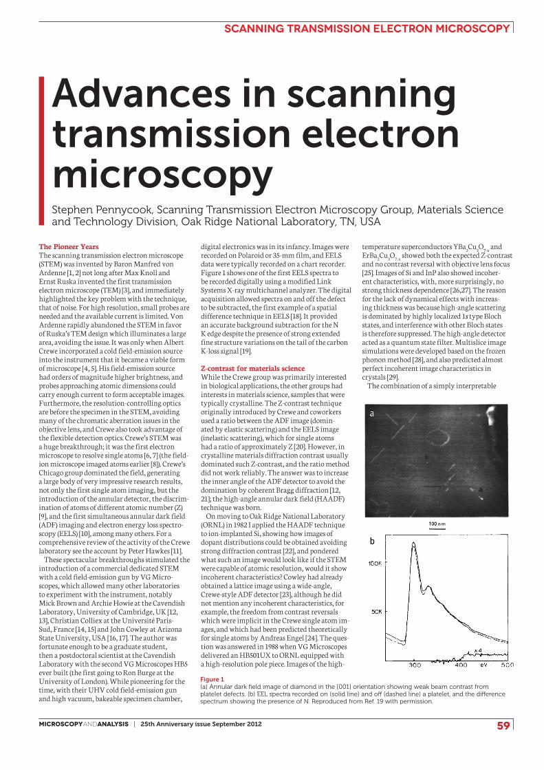
Figure 1(a) Annular dark field image of diamond in the [001] orientation showing weak beam contrast from platelet defects. (b) EEL spectra recorded on (solid line) and off (dashed line) a platelet, and the difference spectrum showing the presence of N. Reproduced from Ref. 19 with permission.
digital electronics was in its infancy. Images were recorded on Polaroid or 35-mm film, and EELS data were typically recorded on a chart recorder. Figure 1 shows one of the first EELS spectra to be recorded digitally using a modified Link Systems X-ray multichannel analyzer. The digital acquisition allowed spectra on and off the defect to be subtracted, the first example of a spatial difference technique in EELS [18]. It provided an accurate background subtraction for the N K edge despite the presence of strong extended fine structure variations on the tail of the carbon K-loss signal [19].
Z-contrast for materials scienceWhile the Crewe group was primarily interested in biological applications, the other groups had interests in materials science, samples that were typically crystalline. The Z-contrast technique originally introduced by Crewe and coworkers used a ratio between the ADF image (domin-ated by elastic scattering) and the EELS image (inelastic scattering), which for single atoms had a ratio of approximately Z [20]. However, in crystalline materials diffraction contrast usually dominated such Z-contrast, and the ratio method did not work reliably. The answer was to increase the inner angle of the ADF detector to avoid the domination by coherent Bragg diffraction [12, 21]; the high-angle annular dark field (HAADF) technique was born.
On moving to Oak Ridge National Laboratory (ORNL) in 1982 I applied the HAADF technique to ion-implanted Si, showing how images of dopant distributions could be obtained avoiding strong diffraction contrast [22], and pondered what such an image would look like if the STEM were capable of atomic resolution, would it show incoherent characteristics? Cowley had already obtained a lattice image using a wide-angle, Crewe-style ADF detector [23], although he did not mention any incoherent characteristics, for example, the freedom from contrast reversals which were implicit in the Crewe single atom im-ages, and which had been predicted theoretically for single atoms by Andreas Engel [24]. The ques-tion was answered in 1988 when VG Microscopes delivered an HB501UX to ORNL equipped with a high-resolution pole piece. Images of the high-
temperature superconductors YBa2Cu3O7-x and ErBa2Cu3O7-x showed both the expected Z-contrast and no contrast reversal with objective lens focus [25]. Images of Si and InP also showed incoher-ent characteristics, with, more surprisingly, no strong thickness dependence [26,27]. The reason for the lack of dynamical effects with increas-ing thickness was because high-angle scattering is dominated by highly localized 1s type Bloch states, and interference with other Bloch states is therefore suppressed. The high-angle detector acted as a quantum state filter. Multislice image simulations were developed based on the frozen phonon method [28], and also predicted almost perfect incoherent image characteristics in crystals [29].
The combination of a simply interpretable
scanning transmission electron microscopy
60 25th Anniversary issue September 2012 | MicroscopyandAnalysis
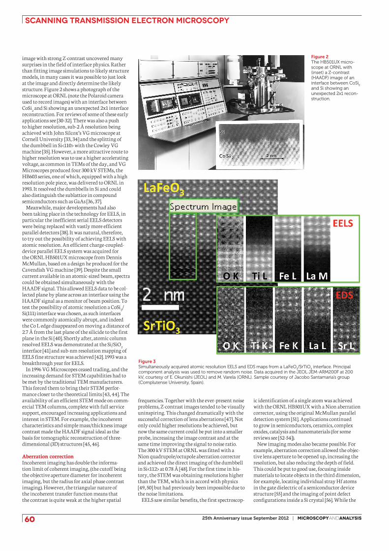
image with strong Z-contrast uncovered many surprises in the field of interface physics. Rather than fitting image simulations to likely structure models, in many cases it was possible to just look at the image and directly determine the likely structure. Figure 2 shows a photograph of the microscope at ORNL (note the Polaroid camera used to record images) with an interface between CoSi2 and Si showing an unexpected 2x1 interface reconstruction. For reviews of some of these early applications see [30-32]. There was also a push to higher resolution, sub-2 Å resolution being achieved with John Silcox’s VG microscope at Cornell University [33, 34] and the splitting of the dumbbell in Si<110> with the Cowley VG machine [35]. However, a more attractive route to higher resolution was to use a higher accelerating voltage, as common in TEMs of the day, and VG Microscopes produced four 300 kV STEMs, the HB603 series, one of which, equipped with a high resolution pole piece, was delivered to ORNL in 1993. It resolved the dumbbells in Si and could also distinguish the sublattice in compound semiconductors such as GaAs [36, 37].
Meanwhile, major developments had also been taking place in the technology for EELS, in particular the inefficient serial EELS detectors were being replaced with vastly more efficient parallel detectors [38]. It was natural, therefore, to try out the possibility of achieving EELS with atomic resolution. An efficient charge-coupled-device parallel EELS system was acquired for the ORNL HB501UX microscope from Dennis McMullan, based on a design he produced for the Cavendish VG machine [39]. Despite the small current available in an atomic-sized beam, spectra could be obtained simultaneously with the HAADF signal. This allowed EELS data to be col-lected plane by plane across an interface using the HAADF signal as a monitor of beam position. To test the possibility of atomic resolution a CoSi2/Si(111) interface was chosen, as such interfaces were commonly atomically abrupt, and indeed the Co L edge disappeared on moving a distance of 2.7 Å from the last plane of the silicide to the first plane in the Si [40]. Shortly after, atomic column resolved EELS was demonstrated at the Si/SiO2 interface [41] and sub-nm resolution mapping of EELS fine structure was achieved [42]. 1993 was a breakthrough year for EELS.
In 1996 VG Microscopes ceased trading, and the increasing demand for STEM capabilities had to be met by the traditional TEM manufacturers. This forced them to bring their STEM perfor-mance closer to the theoretical limits [43, 44]. The availability of an efficient STEM mode on comm-ercial TEM columns, complete with full service support, encouraged increasing applications and interest in STEM. For example, the incoherent characteristics and simple mass/thickness image contrast made the HAADF signal ideal as the basis for tomographic reconstruction of three-dimensional (3D) structures [45, 46].
Aberration correctionIncoherent imaging has double the informa-tion limit of coherent imaging, (the cutoff being the objective aperture diameter for incoherent imaging, but the radius for axial phase contrast imaging). However, the triangular nature of the incoherent transfer function means that the contrast is quite weak at the higher spatial
frequencies. Together with the ever-present noise problems, Z-contrast images tended to be visually uninspiring. This changed dramatically with the successful correction of lens aberrations [47]. Not only could higher resolutions be achieved, but now the same current could be put into a smaller probe, increasing the image contrast and at the same time improving the signal to noise ratio. The 300 kV STEM at ORNL was fitted with a Nion quadrupole/octupole aberration corrector and achieved the direct imaging of the dumbbell in Si<112> at 0.78 Å [48]. For the first time in his-tory, the STEM was obtaining resolutions higher than the TEM, which is in accord with physics [49, 50] but had previously been impossible due to the noise limitations.
EELS saw similar benefits, the first spectroscop-
Figure 2 The HB501UX micro-scope at ORNL with (inset) a Z-contrast (HAADF) image of an interface between CoSi
2
and Si showing an unexpected 2x1 recon-struction.
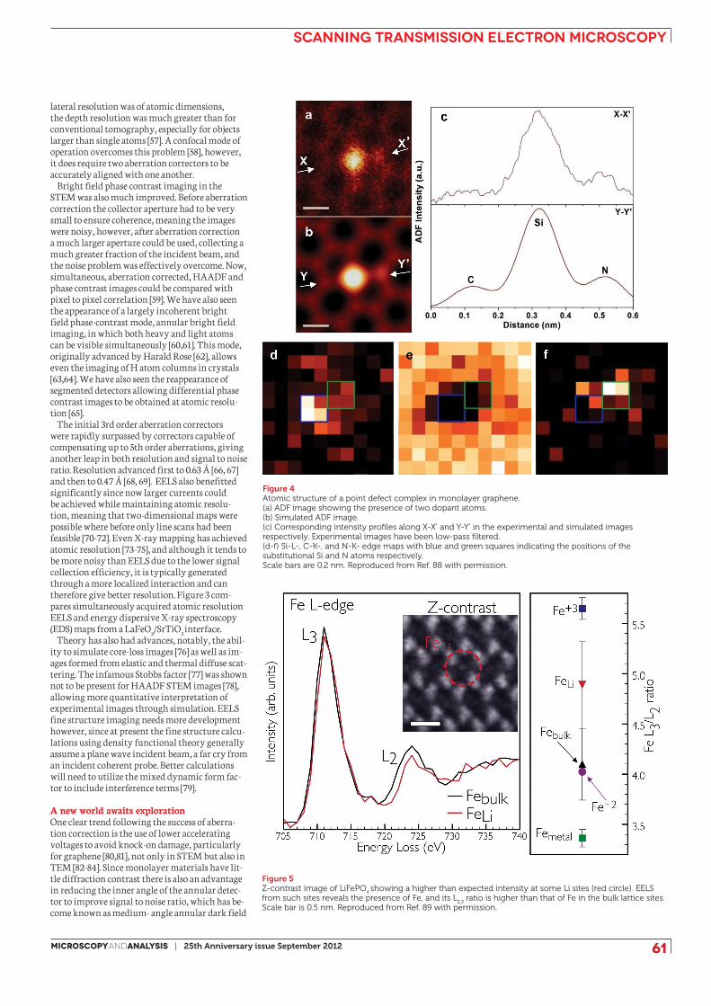
Figure 3 Simultaneously acquired atomic resolution EELS and EDS maps from a LaFeO
3/SrTiO
3 interface. Principal
component analysis was used to remove random noise. Data acquired in the JEOL JEM-ARM200F at 200 kV, courtesy of E. Okunishi (JEOL) and M. Varela (ORNL). Sample courtesy of Jacobo Santamaria’s group (Complutense University, Spain).
ic identification of a single atom was achieved with the ORNL HB501UX with a Nion aberration corrector, using the original McMullan parallel detection system [51]. Applications continued to grow in semiconductors, ceramics, complex oxides, catalysis and nanomaterials (for some reviews see [52-54]).
New imaging modes also became possible. For example, aberration correction allowed the objec-tive lens aperture to be opened up, increasing the resolution, but also reducing the depth of field. This could be put to good use, focusing inside materials to locate objects in the third dimension, for example, locating individual stray Hf atoms in the gate dielectric of a semiconductor device structure [55] and the imaging of point defect configurations inside a Si crystal [56]. While the
scanning transmission electron microscopy
61MicroscopyandAnalysis | 25th Anniversary issue September 2012
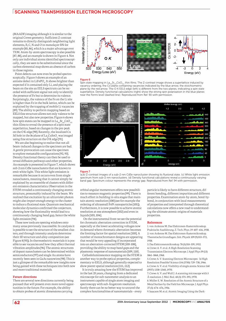
Figure 4Atomic structure of a point defect complex in monolayer graphene. (a) ADF image showing the presence of two dopant atoms.(b) Simulated ADF image. (c) Corresponding intensity profiles along X-X’ and Y-Y’ in the experimental and simulated images respectively. Experimental images have been low-pass filtered. (d-f) Si-L-, C-K-, and N-K- edge maps with blue and green squares indicating the positions of the substitutional Si and N atoms respectively. Scale bars are 0.2 nm. Reproduced from Ref. 88 with permission.
Figure 5Z-contrast image of LiFePO
4 showing a higher than expected intensity at some Li sites (red circle). EELS
from such sites reveals the presence of Fe, and its L2,3
ratio is higher than that of Fe in the bulk lattice sites. Scale bar is 0.5 nm. Reproduced from Ref. 89 with permission.
lateral resolution was of atomic dimensions, the depth resolution was much greater than for conventional tomography, especially for objects larger than single atoms [57]. A confocal mode of operation overcomes this problem [58], however, it does require two aberration correctors to be accurately aligned with one another.
Bright field phase contrast imaging in the STEM was also much improved. Before aberration correction the collector aperture had to be very small to ensure coherence, meaning the images were noisy, however, after aberration correction a much larger aperture could be used, collecting a much greater fraction of the incident beam, and the noise problem was effectively overcome. Now, simultaneous, aberration corrected, HAADF and phase contrast images could be compared with pixel to pixel correlation [59]. We have also seen the appearance of a largely incoherent bright field phase-contrast mode, annular bright field imaging, in which both heavy and light atoms can be visible simultaneously [60,61]. This mode, originally advanced by Harald Rose [62], allows even the imaging of H atom columns in crystals [63,64]. We have also seen the reappearance of segmented detectors allowing differential phase contrast images to be obtained at atomic resolu-tion [65].
The initial 3rd order aberration correctors were rapidly surpassed by correctors capable of compensating up to 5th order aberrations, giving another leap in both resolution and signal to noise ratio. Resolution advanced first to 0.63 Å [66, 67] and then to 0.47 Å [68, 69]. EELS also benefitted significantly since now larger currents could be achieved while maintaining atomic resolu-tion, meaning that two-dimensional maps were possible where before only line scans had been feasible [70-72]. Even X-ray mapping has achieved atomic resolution [73-75], and although it tends to be more noisy than EELS due to the lower signal collection efficiency, it is typically generated through a more localized interaction and can therefore give better resolution. Figure 3 com-pares simultaneously acquired atomic resolution EELS and energy dispersive X-ray spectroscopy (EDS) maps from a LaFeO3/SrTiO3 interface.
Theory has also had advances, notably, the abil-ity to simulate core-loss images [76] as well as im-ages formed from elastic and thermal diffuse scat-tering. The infamous Stobbs factor [77] was shown not to be present for HAADF STEM images [78], allowing more quantitative interpretation of experimental images through simulation. EELS fine structure imaging needs more development however, since at present the fine structure calcu-lations using density functional theory generally assume a plane wave incident beam, a far cry from an incident coherent probe. Better calculations will need to utilize the mixed dynamic form fac-tor to include interference terms [79].
A new world awaits explorationOne clear trend following the success of aberra-tion correction is the use of lower accelerating voltages to avoid knock-on damage, particularly for graphene [80,81], not only in STEM but also in TEM [82-84]. Since monolayer materials have lit-tle diffraction contrast there is also an advantage in reducing the inner angle of the annular detec-tor to improve signal to noise ratio, which has be-come known as medium- angle annular dark field
scanning transmission electron microscopy
62 25th Anniversary issue September 2012 | MicroscopyandAnalysis
Figure 7(a,b) Z-contrast images of a sub-2 nm CdSe nanocluster showing its fluxional state. (c) White light emission spectrum from sub-2 nm nanoclusters. (d) Density functional calculations reveal a continuously varying band gap. Spectrum colour represents the energy gap. Reproduced from Ref. 94 with permission.
(MAADF) imaging although it is similar to the original Crewe geometry. Sufficient Z-contrast remains to directly distinguish neighboring light elements, B, C, N and O in monolayer BN for example [85, 86], which is a major advantage over TEM. Atom-by-atom spectroscopy is also possible [87, 88], and an example is shown in Figure 4. Not only are individual atoms identified spectroscopi-cally, they are seen to be substitutional since the carbon elemental map shows an absence of carbon in those regions.
Point defects can now even be probed spectro-scopically. Figure 5 shows an example of an antisite defect in LiFePO4. It shows brighter than expected if it contained only Li, and placing the beam on the site an EELS spectrum can be rec-orded with sufficient signal not only to identify the presence of Fe but to determine its valence. Surprisingly, the valence of the Fe on the Li site is higher than Fe in the bulk lattice, which can be explained by the trapping of mobile Li vacancies [89]. The ability to perform mapping based on EELS fine structure allows not only valence to be mapped, but also new properties. Figure 6 shows how spin states can be mapped in La0.5Sr0.5CoO3-d thin films to reveal the presence of a spin state superlattice, based on changes in the pre-peak on the O K edge [90]. Recently, the localized Cu 3d hole in the bc plane of La2CuSnO6 was imaged using fine structure on the O K edge [91].
We are also beginning to realize that not all beam-induced changes to the specimen are bad. A gentle provocation can cause the specimen to explore metastable configurations [92, 93]. Density functional theory can then be used to reveal diffusion pathways and other properties. An example is presented in Figure 7, which shows sub-2 nm CdSe nanoclusters that are known to emit white light. This white light emission is remarkable because it occurs even from single nanoclusters, meaning that it cannot simply be explained by an ensemble of clusters with differ-ent emission characteristics. Observation in the STEM revealed a continuously changing atomic structure, presumably induced by the beam. We realized that excitation by an ultraviolet photon might also impart enough energy to the cluster to induce a fluxional state. Quantum mechanical molecular dynamics confirmed the conjecture, showing how the fluxionality would lead to a continuously changing band gap, hence the white light emission [94].
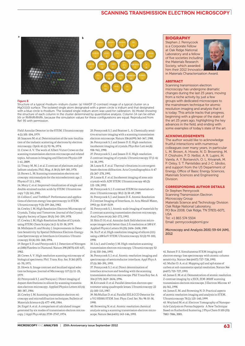
These new tools are opening windows onto many areas previously inaccessible. In catalysis it is possible to see the structure of the smallest clus-ters, and through intensity analysis determine their 3D structure and alloy composition (see Figure 8 [95]). In thermoelectric materials it is pos-sible to see vacancies and how they affect thermal vibration amplitudes [96]. The atomic structures of dopant nanoclusters can be determined within semiconductors [97] and single Au atoms have recently been seen in GaAs nanowires [98]. This is just a glimpse of the remarkable new insights now being gained with these techniques into both new and more traditional materials.
Future directionsThere are several new directions currently being pursued that will present even more novel oppor- tunities in the future. For example, the ability to obtain probes of atomic dimensions carrying
particle is likely to have different structure, dif-ferent bonding, different impurities and different properties. Examination atom-by-atom, bond-by-bond, in conjunction with local measurements of properties and interpreted through theoretical calculations now offers a new road to understand-ing the ultimate atomic origins of materials properties.
References 1. von Ardenne M. Das Elektronen-Rastermikroskop. Praktische Ausführung. Z. Tech. Phys. 19: 407–416, 1938.2. von Ardenne M. Das Elektronen-Rastermikroskop. Theoretische Grundlagen. Zeit. Physik 109 (9):553–572, 1938.3. Das Elektronenmikroskop. 78 (5):318–339, 1932.4. Crewe A. V. et al. A High-Resolution Scanning Transmission Electron Microscope. J Appl Phys 39 (13) 5861–5868, 1968.5. Crewe A. V. Scanning Electron Microscopes - Is High Resolution Possible? Science 154 (3750): 729–738, 1966.6. Crewe A. V. et al. Visibility of single atoms. Science 168 (3937): 1338–1340, 1970.7. Crewe A. V. and Wall J. A scanning microscope with 5 Å resolution. J. Mol. Biol. 48 (3): 375–393, 1970.8. Müller E. W. Resolution of the Atomic Structure of a Metal Surface by the Field Ion Microscope. J Appl Phys 27 (5): 474–476, 1956.9. Isaacson M. et al. Atomic Imaging Using the Dark-
orbital angular momentum offers new possibili-ties to measure magnetic properties [99]. There is much effort in building in-situ stages that main-tain atomic resolution [100] (see for example the ordering of ultrasmall FePt nanoparticles [101]). Furthermore, it is now possible to achieve atomic resolution at one atmosphere [102] and even in liquids [103, 104].
On the instrumental front we see the potential for chromatic aberration correction in STEM, especially at the lower accelerating voltages now in demand where chromatic aberration becomes the limiting factor for spatial resolution [105]. A number of monochromator designs are appearing that would be very appealing if incorporated into an aberration-corrected STEM [105-108], providing the ability to map band gaps and the plasmonic response of nanomaterials [109, 110] .
Cathodoluminescence mapping on the STEM is another way to probe optical properties, comple-mentary to EELS, although generally expected to show poorer spatial resolution [111, 112].
It is truly amazing how the STEM has improved in the last 25 years, changing from a dedicated microscope for sub-nanometer analysis to an instrument capable of single atom imaging and spectroscopy with sub-Ångstrom resolution. Surely there can be no better way to unravel the complex functionalities of nanomaterials – every
Figure 6Spin state mapping in La
0.5Sr
0.5CoO
3-d thin films. The Z-contrast image shows a superlattice induced by vacancy ordering, the Co plane containing vacancies indicated by the blue arrow, the stoichiometric plane by the red arrow. The O K EELS edge (left) is different from the two planes, indicating a spin state superlattice. Density functional calculations (right) show the strong spin polarization in the blue planes near the Fermi level (dashed line). Reproduced from Ref. 90 with permission.
scanning transmission electron microscopy
63MicroscopyandAnalysis | 25th Anniversary issue September 2012
biography Stephen J. Pennycook is a Corporate Fellow at Oak Ridge National Laboratory and a fellow of five societies including the Materials Research Society, which awarded him their 2012 Innovation in Materials Characterization Award.
abstractScanning transmission electron microscopy has undergone dramatic changes during the last 25 years, moving from a niche activity by just a few groups with dedicated microscopes to the mainstream technique for atomic resolution imaging and analysis that it is today. This article tracks that progress, beginning with a glimpse of the state of the art 25 years ago, highlighting the key advances in the field, and ending with some examples of today’s state of the art.
acknowledgements The author would like to acknowledge fruitful interactions with numerous colleagues over many years, in particular L. M. Brown, A. Howie, N. D. Browning, M. F. Chisholm, P. D. Nellist, A. R. Lupini, M. Varela, A. Y. Borisevich, O. L. Krivanek, M. P. Oxley, S. T. Pantelides and J-C. Idrobo, and support from the US Department of Energy, Office of Basic Energy Sciences, Materials Sciences and Engineering Division.
corresponding author details Dr Stephen Pennycook Scanning Transmission Electron Microscopy GroupMaterials Science and Technology DivisionOak Ridge National Laboratory, PO Box 2008, Oak Ridge, TN 37831-6071, USATel: +1 865 574 5504 Email: [email protected]
Microscopy and Analysis 26(6):59-64 (AM), 2012
Field Annular Detector in the STEM. Ultramicroscopy 4 (1): 101–104, 1979.10. Isaacson M. et al. Determination of the non-localiza-tion of the inelastic scattering of electrons by electron microscopy. Optik 41 (1): 92–96, 1974.11. Crewe A. V. The work of Albert Victor Crewe on the scanning transmission electron microscope and related topics. Advances in Imaging and Electron Physics 159 1–61, 2009.12. Treacy M. M. J. et al. Z contrast of platinum and pal-ladium catalysts. Phil. Mag. A 38 (5): 569–585, 1978.13. Brown L. M. Scanning transmission electron mi-croscopy: microanalysis for the microelectronic age. J. Physics F 11 1, 1981.14. Mory C. et al. Improved visualization of single-and double-strained nucleic acids by STEM. Ultramicros-copy 7 (2): 161, 1981.15. Colliex C. and Trebbia P. Performance and applica-tions of electron energy loss spectroscopy in STEM. Ultramicroscopy 9 (3): 259–266, 1982.16. Cowley J. M. High Resolution Electron Microscopy of Crystals, Today and Tomorrow. Journal of the Crystal-logrphy Society of Japan 20 (5): 241–259, 1978.17. Cowley J. M. High-Resolution Studies of Crystals using STEM. Chem Scripta 14 (1-5): 33–38, 1979.18. Müllejans H. and Bruley J. Improvements in Detec-tion Sensitivity by Spatial Difference Electron-Energy-Loss Spectroscopy at Interfaces in Ceramics. Ultrami-croscopy 53 (4): 351–360, 1994.19. Berger S. D. and Pennycook S. J. Detection of Nitrogen at (100) Platelets in Diamond. Nature 298 (5875): 635–637, 1982.20. Crewe A. V. High resolution scanning microscopy of biological specimens. Phil. Trans. Roy. Soc. B 261 (837): 61–70, 1971.21. Howie A. Image contrast and localized signal selec-tion techniques. Journal of Microscopy 117 (1): 11–23, 1979.22. Pennycook S. J. and Narayan J. Direct imaging of dopant distributions in silicon by scanning transmis-sion electron microscopy. Applied Physics Letters 45 (4): 385–387, 1984.23. Cowley J. M. Scanning transmission electron mi-croscopy and microdiffraction techniques. Bulletin of Materials Science 6 (3): 477–490, 1984.24. Engel A. et al. A comparison of calculated images generated by six modes of transmission electron micros-copy. J Appl Phys 45 (6): 2739–2747, 1974.
Figure 8Structure of a typical rhodium–iridium cluster. (a) HAADF (Z-contrast) image of a typical cluster on a MgO(110) surface. The isolated single atom designated with a green circle is iridium and that designated with a blue circle is rhodium. The isolated single iridium atom was used for calibration. (b) Model showing the structure of each column in the cluster determined by quantitative analysis. Column 14 can be either IrIr or RhRhRhRhRh, because the simulation values for these configurations are equal. Reproduced from Ref. 95 with permission.
25. Pennycook S. J. and Boatner L. A. Chemically sensi-tive structure-imaging with a scanning transmission electron microscope. Nature 336 (6199): 565–567, 1988.26. Pennycook S. J. and Jesson D. E. High-resolution incoherent imaging of crystals. Phys Rev Lett 64 (8): 938–941, 1990.27. Pennycook S. J. and Jesson D. E. High-resolution Z-contrast imaging of crystals. Ultramicroscopy 37 (1-4): 14–38, 1991.28. Loane R. F. et al. Thermal vibrations in convergent-beam electron diffraction. Acta Crystallographica A 47 (3): 267–278, 1991.29. Loane R. F. et al. Incoherent imaging of zone axis crystals with ADF STEM. Ultramicroscopy 40 (2): 121–138, 1992.30. Pennycook S. J. Z-contrast STEM for materials sci-ence. Ultramicroscopy 30 (1-2): 58–69, 1989.31. Pennycook S. J. and Jesson D. E. Atomic Resolution Z-Contrast Imaging of Interfaces, in: Acta Metall Mater, 1992: pp. S149–S159.32. Pennycook S. J. Atomic-scale imaging of materials by Z-contrast scanning transmission electron microscopy. Anal Chem 64 (4): 263–272, 1992.33. Shin D. H. et al. Annular dark field electron micro-scope images with better than 2 Å resolution at 100 kV. Applied Physics Letters 55 (23): 2456–2458, 1989.34. Xu P. et al. High-resolution imaging of silicon (111) using a 100 keV STEM. Ultramicroscopy 32 (2): 93–102, 1990.35. Liu J. and Cowley J. M. High-resolution scanning transmission electron microscopy. Ultramicroscopy 52 (3-4): 335–346, 1993.36. Pennycook S. J. et al. Atomic-resolution imaging and spectroscopy of semiconductor interfaces. Appl Phys A 57 (5): 385–391, 1993.37. Pennycook S. J. et al. Direct determination of interface structure and bonding with the scanning transmission electron microscope. Phil Trans Roy Soc A 354 (1719): 2619–2634, 1996.38. Krivanek O. et al. Parallel detection electron spec-trometer using quadrupole lenses. Ultramicroscopy 22 (1): 103–115, 1987.39. McMullan D. et al. Parallel EELS CCD Detector for a VG HB501 STEM. Inst. Phys. Conf. Ser. No. 98: 55–58, 1990.40. Browning N. et al. Atomic-resolution chemical analysis using a scanning transmission electron micro-scope. Nature 366 (6451): 143–146, 1993.
41. Batson P. E. Simultaneous STEM imaging and electron energy-loss spectroscopy with atomic-column sensitivity. Nature 366 (6457): 727–728, 1993.42. Muller D. A. et al. Mapping sp2 and sp3 states of carbon at sub-nanometre spatial resolution. Nature 366 (6457): 725–727, 1993.43. James E. M. et al. Demonstration of atomic resolution Z-contrast imaging by a JEOL JEM-2010F scanning transmission electron microscope. J Electron Microsc 47 (6): 561, 1998.44. James E. M. and Browning N. D. Practical aspects of atomic resolution imaging and analysis in STEM. Ultramicroscopy 78 (1): 125–140, 1999.45. Weyland M. et al. Electron Tomography of Nanopar-ticle Catalysts on Porous Supports A New Technique Based on Rutherford Scattering. J Phys Chem B 105 (33): 7882–7886, 2001.
scanning transmission electron microscopy
64 25th Anniversary issue September 2012 | MicroscopyandAnalysis
46. Midgley P. A. et al. Z-Contrast tomography: a tech-nique in three-dimensional nanostructural analysis based on Rutherford scattering. Chem Commun (10): 907–908, 2001.47. Batson P. E. et al. Sub-angstrom resolution using aberration corrected electron optics. Nature 418 (6898): 617–620, 2002.48. Nellist P. D. et al. Direct sub-angstrom imaging of a crystal lattice. Science 305 (5691): 1741–1741, 2004.49. Rayleigh L. On the theory of optical images with special reference to the microscope. Phil Mag 42 (255): 167–195, 1896.50. Scherzer O. The theoretical resolution limit of the electron microscope. J Appl Phys 20 (1): 20–29, 1949.51. Varela M. et al. Spectroscopic imaging of single atoms within a bulk solid. Phys Rev Lett 92 (9): 95502, 2004.52. Pennycook S. J. et al. Materials advances through aberration-corrected electron microscopy. MRS Bull. 31 (01): 36–43, 2006.53. Varela M. et al. Materials characterization in the aberration-corrected scanning transmission electron microscope. Annu Rev Mater Res 35 539–569, 2005.54. Pennycook S. J. et al. Aberration-corrected scanning transmission electron microscopy: from atomic imag-ing and analysis to solving energy problems. Phil Trans Roy Soc A 367 (1903): 3709–3733, 2009.55. van Benthem K. et al. Three-dimensional imaging of individual hafnium atoms inside a semiconductor device. Appl Phys Lett 87 (3): 034104, 2005.56. Oh S. et al. Point Defect Configurations of Supersatu-rated Au Atoms Inside Si Nanowires. Nano Lett 8 (4): 1016–1019, 2008.57. Borisevich A. Y. et al. Depth sectioning with the aberration-corrected scanning transmission electron microscope. Proc. Nat. Acad. Sci. USA 103 (9): 3044–3048, 2006.58. Nellist P. D. et al. Confocal operation of a transmis-sion electron microscope with two aberration correc-tors. Appl Phys Lett 89 (12): 124105, 2006.59. Pennycook S. J. Transmission Electron Microscopy, in: F. Bassani, J. Liedl, P. Wyder (Eds.), Encyclopedia of Condensed Matter Physics, Elsevier, 2006: pp. 240–247.60. Findlay S. D. et al. Dynamics of annular bright field imaging in scanning transmission electron microscopy. Ultramicroscopy 110 (7): 903–923, 2010.61. Findlay S. D. et al. Robust atomic resolution imaging of light elements using scanning transmission electron microscopy. Appl Phys Lett 95 (19): 191913, 2009.62. Rose H. Phase-contrast in scanning transmission electron microscopy. Optik 39 (4): 416–436, 1974.63. Ishikawa R. et al. Direct imaging of hydrogen-atom columns in a crystal by annular bright-field electron microscopy. Nature Materials 10 (4): 278–281, 2011.64. Findlay S. D. et al. Direct imaging of hydrogen within a crystalline environment. Applied Physics Express 3 (11): 6603, 2010.65. Shibata N. et al. Differential phase-contrast micros-copy at atomic resolution. Nat Phys 8 (7): 1–5, 2012.66. Sawada H. et al. Achieving 63 pm resolution in scan-ning transmission electron microscope with spherical aberration corrector. Jpn J Appl Phys 46 L568–L570, 2007.67. Kisielowski C. et al. Detection of single atoms and buried defects in three dimensions by aberration-cor-rected electron microscope with 0.5-angstrom informa-tion limit. Microsc Microanal 14 (5): 469–477, 2008.68. Sawada H. et al. STEM imaging of 47-pm-separated atomic columns by a spherical aberration-corrected electron microscope with a 300-kV cold field emission gun. J Electron Microsc 58 (6): 357, 2009.69. Erni R. et al. Atomic-resolution imaging with a sub-50-pm electron probe. Phys Rev Lett 102 (9): 96101, 2009.
70. Bosman M. et al. Two-dimensional mapping of chemical information at atomic resolution. Phys Rev Lett 99 (8): 86102, 2007.71. Varela M. et al. Atomic-resolution imaging of oxida-tion states in manganites. Phys Rev B 79 (8): 085117, 2009.72. Muller D. A. et al. Atomic-Scale Chemical Imaging of Composition and Bonding by Aberration-Corrected Microscopy. Science 319 (5866): 1073–1076, 2008.73. D’Alfonso A. et al. Atomic-resolution chemical map-ping using energy-dispersive x-ray spectroscopy. Phys Rev B 81 (10): 100101, 2010.74. Chu M.-W. et al. Emergent Chemical Mapping at Atomic-Column Resolution by Energy-Dispersive X-Ray Spectroscopy in an Aberration-Corrected Electron Microscope. Phys Rev Lett 104 (19): 196101, 2010.75. Lovejoy T. C. et al. Single atom identification by energy dispersive x-ray spectroscopy. Appl Phys Lett 100 (15): 154101, 2012.76. Allen L. et al. Modelling high-resolution electron microscopy based on core-loss spectroscopy. Ultrami-croscopy 106 (11-12): 1001–1011, 2006.77. Hÿtch M. and Stobbs W. M. Quantitative compari-son of high resolution TEM images with image simula-tions. Ultramicroscopy 53 (3): 191–203, 1994.78. LeBeau J. M. et al. Quantitative atomic resolution scanning transmission electron microscopy. Phys Rev Lett 100 (20): 206101, 2008.79. Witte C. et al. Theory of dynamical scattering in near-edge electron energy loss spectroscopy. Phys Rev B 80 (18): 184108, 2009.80. Gass M. H. et al. Free-standing graphene at atomic resolution. Nature Nanotechnology 3 (11): 676–681, 2008.81. Huang P. Y. et al. Grains and grain boundaries in single-layer graphene atomic patchwork quilts. Nature 469 (7330): 389–392, 2011.82. Meyer J. C. et al. Direct Imaging of Lattice Atoms and Topological Defects in Graphene Membranes. Nano Lett 8 (11): 3582–3586, 2008.83. Girit C. et al. Graphene at the edge: stability and dynamics. Science 323 (5922): 1705, 2009.84. Meyer J. C. Experimental analysis of charge redis-tribution due to chemical bonding by high-resolution transmission electron microscopy. Nature Materials 10 (3): 209–215, 2011.85. Krivanek O. L. et al. Gentle STEM ADF imaging and EELS at low primary energies. Ultramicroscopy 110 (8): 935–945, 2010.86. Krivanek O. L. et al. Atom-by-atom structural and chemical analysis by annular dark-field electron mi-croscopy. Nature 464 (7288): 571–574, 2010.87. Suenaga K. and Koshino M. Atom-by-atom spectros-copy at graphene edge. Nature 468 (7327): 1088–1090, 2010.88. Zhou W. et al. Atomically localized plasmon en-hancement in monolayer graphene. Nature Nanotech-nology 7 (3) :161–165, 2012.89. Lee J. et al. Vacancy-Driven Anisotropic Defect Distribution in the Battery-Cathode Material LiFePO4. Phys Rev Lett 107 (8): 85507, 2011.90. Gazquez J. et al. Atomic-Resolution Imaging of Spin-State Superlattices in Nanopockets within Cobaltite Thin Films. Nano Lett 11 (3): 973–976, 2011.91. Haruta M. et al. Visualization of hybridization states with atomic resolution using electron energy loss spec-troscopy mapping. Appl Phys Lett 100 (16): 163107, 2012.92. Bals S. S. et al. Atomic scale dynamics of ultrasmall germanium clusters. Nature Communications 3 897–897, 2012.93. Warner J. H. et al. Dislocation-Driven Deformations in Graphene. Science 337 (6091): 209–212, 2012.94. Pennycook T. J. et al. Dynamic Fluctuations in Ultrasmall Nanocrystals Induce White Light Emission.
Nano Lett 12 (6): 3038–3042, 2012.95. Ortalan V. et al. Towards full-structure determina-tion of bimetallic nanoparticles with an aberration-corrected electron microscope. Nature Nanotechnology 5 (12): 843–847, 2010.96. Harada S. et al. Direct Observation of Vacancies and Local Thermal Vibration in Thermoelectric Rhenium Silicide. Applied Physics Express 5 (3): 035203, 2012.97. Couillard M. et al. Three-Dimensional Atomic Struc-ture of Metastable Nanoclusters in Doped Semiconduc-tors. Phys Rev Lett 107 (18): 186104, 2011.98. Bar-Sadan M. et al. Direct Imaging of Single Au Atoms Within GaAs Nanowires. Nano Lett 12 (5): 2352–2356, 2012.99. Verbeeck J. et al. A new way of producing electron vortex probes for STEM. Ultramicroscopy 113 83–87, 2012.100. Allard L. F. et al. Evolution of gold structure during thermal treatment of Au/FeOx catalysts revealed by aberration-corrected electron microscopy. J Electron Microsc 58 (3): 199–212, 2009.101. Delalande M. et al. L10 Ordering of Ultrasmall FePt Nanoparticles Revealed by TEM In Situ Annealing. Journal of Physical Chemistry C 116 (12): 6866–6872, 2012.102. Mehraeen, S, et al. Atomic-resolution scanning transmission electron microscopy at atmospheric pres-sure (submitted for publication).103. Parent L. R. et al. Direct in Situ Observation of Nanoparticle Synthesis in a Liquid Crystal Surfactant Template. ACS Nano 6 (4): 3589–3596, 2012.104. De Jonge N. and Ross F. M. Electron microscopy of specimens in liquid. Nature Nanotechnology 6 (11): 695–704, 2011.105. Krivanek O. L. et al. High-energy-resolution monochromator for aberration-corrected scanning transmission electron microscopy/electron energy-loss spectroscopy. Phil Trans Roy Soc A 367 (1903): 3683–3697, 2009.106. Bell D. C. et al. Sub-Angstrom Low-Voltage Per-formance of a Monochromated, Aberration-Corrected Transmission Electron Microscope. Microsc Microanal 16 (4): 386–392, 2010.107. Essers E. et al. Energy resolution of an Omega-type monochromator and imaging properties of the MAN-DOLINE filter. Ultramicroscopy 110 (8): 971–980, 2010.108. Tiemeijer P. C. et al. Using a monochromator to improve the resolution in TEM to below 0.5 angstrom. Part I: Creating highly coherent monochromated il-lumination. Ultramicroscopy 114 72–81, 2012.109. Nicoletti O. et al. Surface plasmon modes of a single silver nanorod: an electron energy loss study. Opt Express 19 (16): 15371–15379, 2011.110. Sigle W. et al. Electron energy losses in Ag nano-holes—from localized surface plasmon resonances to rings of fire. Optics Letters 34 (14): 2150–2152, 2009.111. Pennycook S. J. Investigating the optical properties of dislocations by scanning transmission electron microscopy. Scanning 30 (4): 287–298, 2008.112. Zagonel L. F. et al. Nanometer Scale Spectral Imag-ing of Quantum Emitters in Nanowires and Its Correla-tion to Their Atomically Resolved Structure. Nano Lett 11 (2): 568–573, 2011.
©2012 John Wiley & Sons, Ltd