foundry wlsi technology for power management...
TRANSCRIPT
© 2016 TSMC, Ltd
1
TSMC Property
2016 PwrSoC
Foundry WLSI Technology for Power Management System Integration
Chuei-Tang Wang, Chih-Lin Chen, Jeng-Shien Hsieh, Victor C.Y. Chang, Douglas Yu
R&D,TSMC
Oct. 2016
© 2016 TSMC, Ltd
2
TSMC Property
2016 PwrSoC
Outline
Motivation PMIC system integration trends
Foundry WLSI technology Portfolio
High Performance Computing System (HPC) on CoWoS VR on CoWoS
Impact of Si interposer
Mobile AP and PMIC System (MAPS) on InFO Power Delivery Network
PVR on InFO
Summary & Outlook
© 2016 TSMC, Ltd
3
TSMC Property
2016 PwrSoC
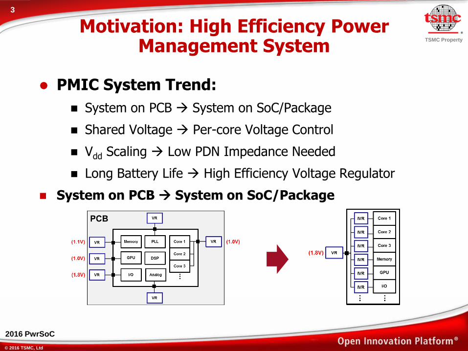
PMIC System Trend:
System on PCB System on SoC/Package
Shared Voltage Per-core Voltage Control
Vdd Scaling Low PDN Impedance Needed
Long Battery Life High Efficiency Voltage Regulator
System on PCB System on SoC/Package
Motivation: High Efficiency Power Management System
© 2016 TSMC, Ltd
4
TSMC Property
2016 PwrSoC
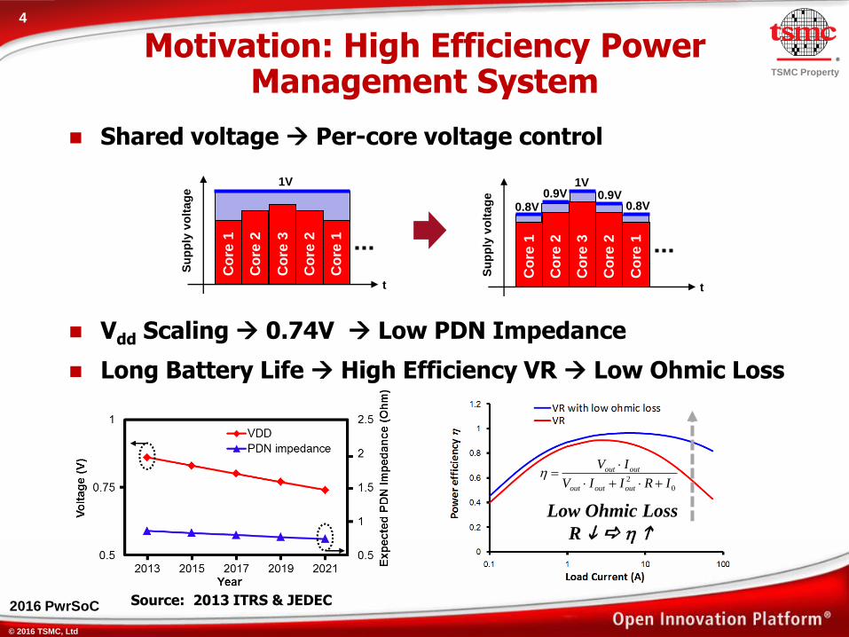
Motivation: High Efficiency Power Management System
Shared voltage Per-core voltage control
Source: 2013 ITRS & JEDEC
Co
re 1
Co
re 2
Co
re 3
1V
0.8V 0.9V
1V
Co
re 2
Co
re 1
t
Su
pp
ly v
olt
ag
e
Co
re 1
Co
re 2
Co
re 3
Co
re 2
Co
re 1
t
Su
pp
ly v
olt
ag
e
0.9V 0.8V
Vdd Scaling 0.74V Low PDN Impedance
Long Battery Life High Efficiency VR Low Ohmic Loss
0
2 IRIIV
IV
outoutout
outout
Low Ohmic Loss
R a h
© 2016 TSMC, Ltd
5
TSMC Property
2016 PwrSoC
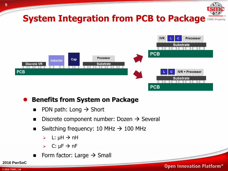
System Integration from PCB to Package
Benefits from System on Package
PDN path: Long Short
Discrete component number: Dozen Several
Switching frequency: 10 MHz 100 MHz
L: μH nH
C: μF nF
Form factor: Large Small
© 2016 TSMC, Ltd
6
TSMC Property
2016 PwrSoC
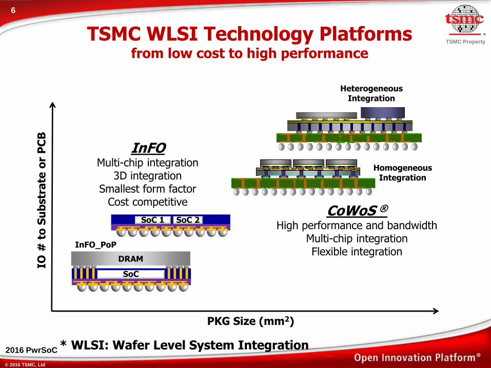
SoC 2 SoC 1
DRAM
SoC
PKG Size (mm2)
IO #
to
Su
bstr
ate
or
PC
B
TSMC WLSI Technology Platforms from low cost to high performance
InFO Multi-chip integration
3D integration Smallest form factor
Cost competitive CoWoS ®
High performance and bandwidth Multi-chip integration Flexible integration
InFO_PoP
Homogeneous Integration
Heterogeneous Integration
* WLSI: Wafer Level System Integration
© 2016 TSMC, Ltd
7
TSMC Property
2016 PwrSoC
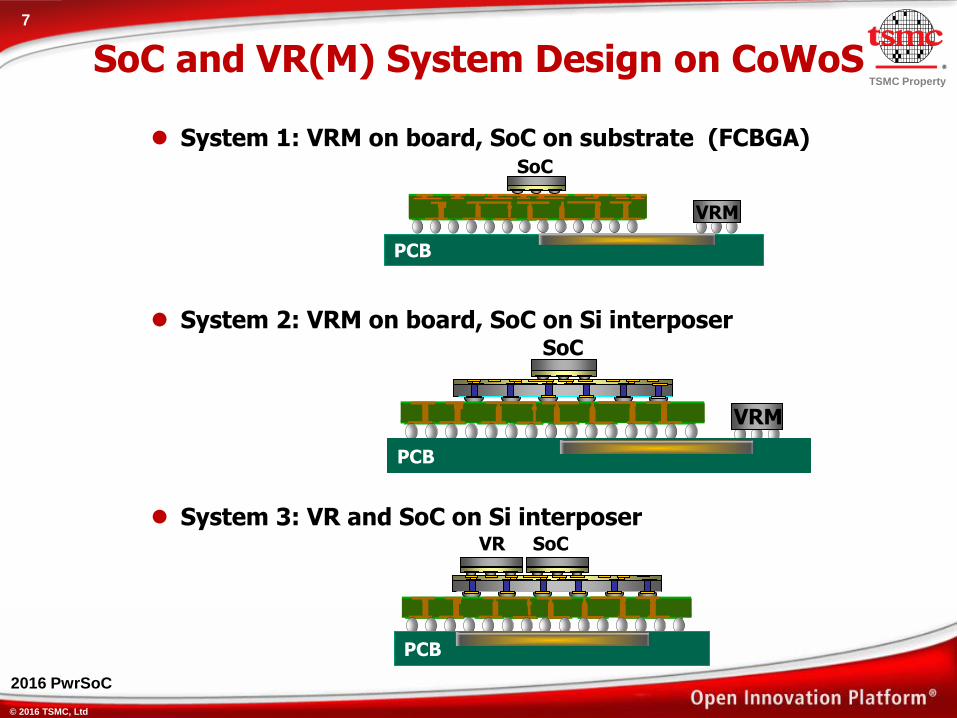
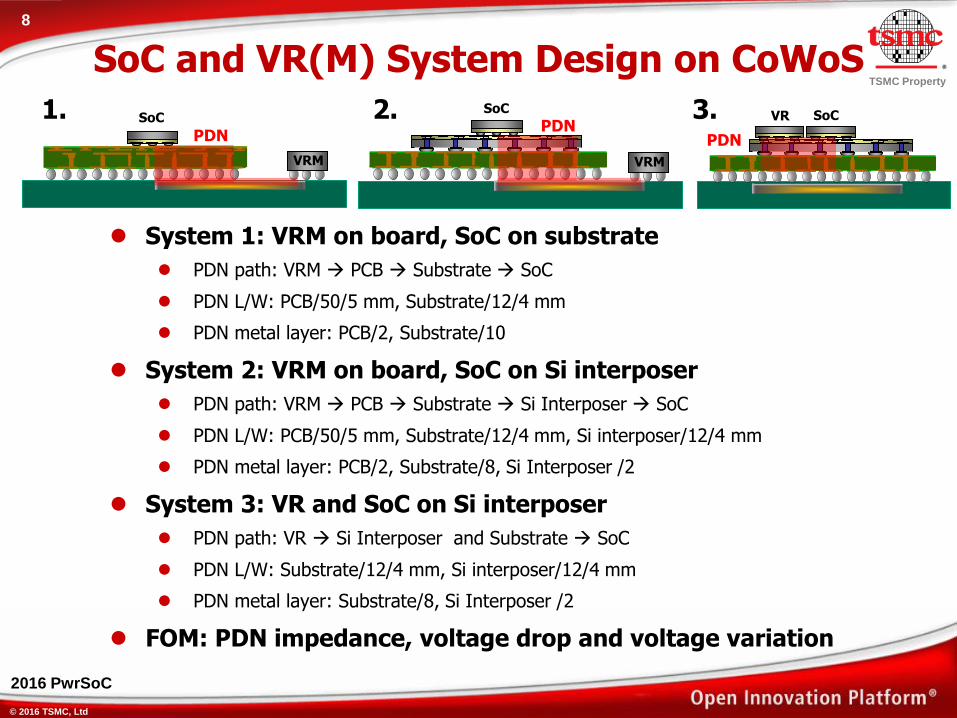
SoC and VR(M) System Design on CoWoS
PCB
SoC VR
System 3: VR and SoC on Si interposer
System 2: VRM on board, SoC on Si interposer
VRM
SoC
PCB
PCB
SoC
VRM
System 1: VRM on board, SoC on substrate (FCBGA)
© 2016 TSMC, Ltd
8
TSMC Property
2016 PwrSoC
SoC and VR(M) System Design on CoWoS
System 1: VRM on board, SoC on substrate
PDN path: VRM PCB Substrate SoC
PDN L/W: PCB/50/5 mm, Substrate/12/4 mm
PDN metal layer: PCB/2, Substrate/10
System 2: VRM on board, SoC on Si interposer
PDN path: VRM PCB Substrate Si Interposer SoC
PDN L/W: PCB/50/5 mm, Substrate/12/4 mm, Si interposer/12/4 mm
PDN metal layer: PCB/2, Substrate/8, Si Interposer /2
System 3: VR and SoC on Si interposer
PDN path: VR Si Interposer and Substrate SoC
PDN L/W: Substrate/12/4 mm, Si interposer/12/4 mm
PDN metal layer: Substrate/8, Si Interposer /2
FOM: PDN impedance, voltage drop and voltage variation
SoC VR 3. PDN
SoC 2.
VRM
PDN SoC 1.
VRM
PDN

© 2016 TSMC, Ltd
9
TSMC Property
2016 PwrSoC
0.01
0.1
1
10
100
1000
0.01 0.1 1 10
PD
N Z
(
)
Frequency (GHz)
2. VRM on board,SoC on Si interposer
3. VR and SoC on Siinterposer
0.01
0.1
1
10
100
1000
0.01 0.1 1 10
PD
N Z
(
)
Frequency (GHz)
1. VRM on board,SoC on Substrate
2. VRM on board,SoC on Si interposer
PDN Impedance Reduction from Si Interposer
Interposer mitigates anti-resonance at high frequencies
Numbers of De-cap to be decreased
Short interconnect reduces PDN impedance: DC and AC
SoC VR 3. PDN
SoC 2.
VRM
PDN SoC 1.
VRM
PDN
© 2016 TSMC, Ltd
10
TSMC Property
2016 PwrSoC
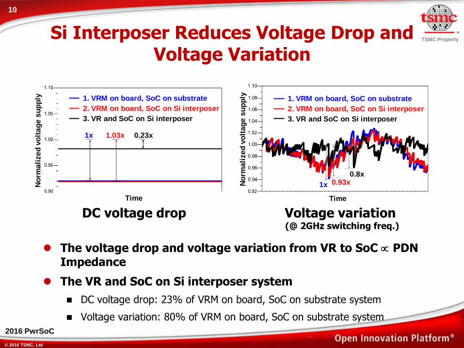
Si Interposer Reduces Voltage Drop and Voltage Variation
DC voltage drop Voltage variation (@ 2GHz switching freq.)
The voltage drop and voltage variation from VR to SoC PDN Impedance
The VR and SoC on Si interposer system
DC voltage drop: 23% of VRM on board, SoC on substrate system
Voltage variation: 80% of VRM on board, SoC on substrate system
Time
No
rma
lize
d v
olt
ag
e s
up
ply
2. VRM on board, SoC on Si interposer
3. VR and SoC on Si interposer
1. VRM on board, SoC on substrate
0.93x0.8x
1x
Time
1.03x 0.23x
No
rma
lize
d v
olt
ag
e s
up
ply
1x
2. VRM on board, SoC on Si interposer
3. VR and SoC on Si interposer
1. VRM on board, SoC on substrate
© 2016 TSMC, Ltd
11
TSMC Property
2016 PwrSoC
0.1
1
10
100
0 1 2 3 4 5 6 7 8 9 10
PD
N Z
(
)
Frequency (GHz)
Si conductivity 0 S/m
Si conductivity 1 S/m
Si conductivity 10 S/m
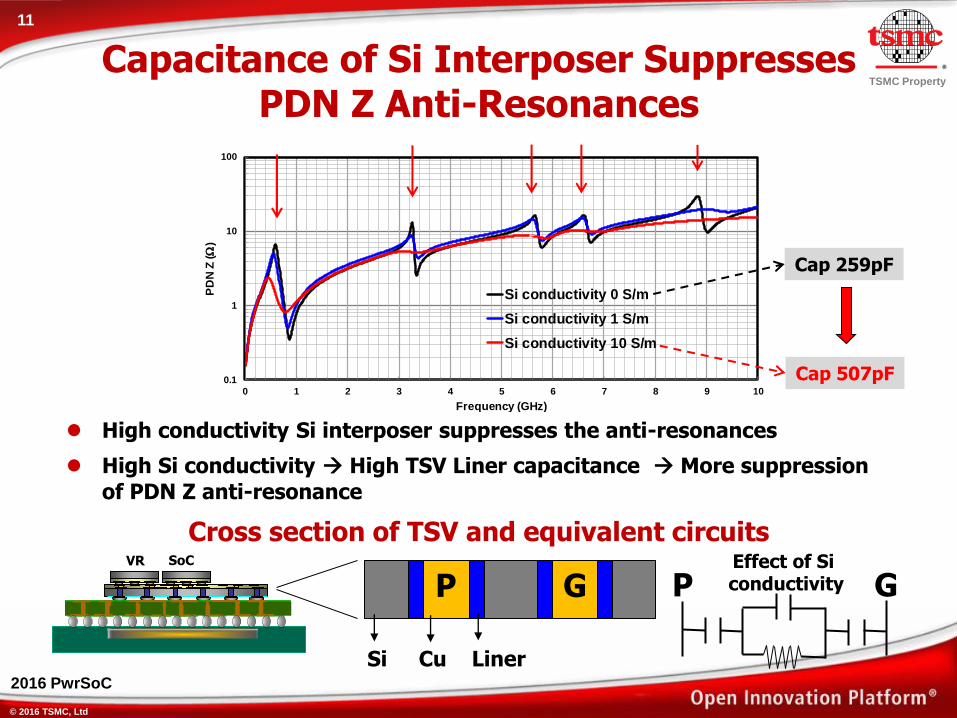
Capacitance of Si Interposer Suppresses PDN Z Anti-Resonances
High conductivity Si interposer suppresses the anti-resonances
High Si conductivity High TSV Liner capacitance More suppression
of PDN Z anti-resonance
Cross section of TSV and equivalent circuits
Si Cu Liner
P G Effect of Si conductivity P G
Cap 259pF
Cap 507pF
SoC VR
© 2016 TSMC, Ltd
12
TSMC Property
2016 PwrSoC
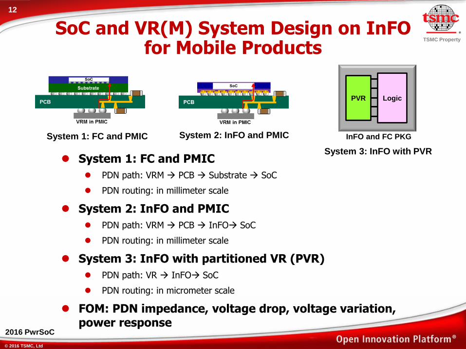
SoC and VR(M) System Design on InFO for Mobile Products
System 1: FC and PMIC
System 1: FC and PMIC
PDN path: VRM PCB Substrate SoC
PDN routing: in millimeter scale
System 2: InFO and PMIC
PDN path: VRM PCB InFO SoC
PDN routing: in millimeter scale
System 3: InFO with partitioned VR (PVR)
PDN path: VR InFO SoC
PDN routing: in micrometer scale
FOM: PDN impedance, voltage drop, voltage variation, power response
System 2: InFO and PMIC
System 3: InFO with PVR
InFO and FC PKG
Logic PVR
© 2016 TSMC, Ltd
13
TSMC Property
2016 PwrSoC
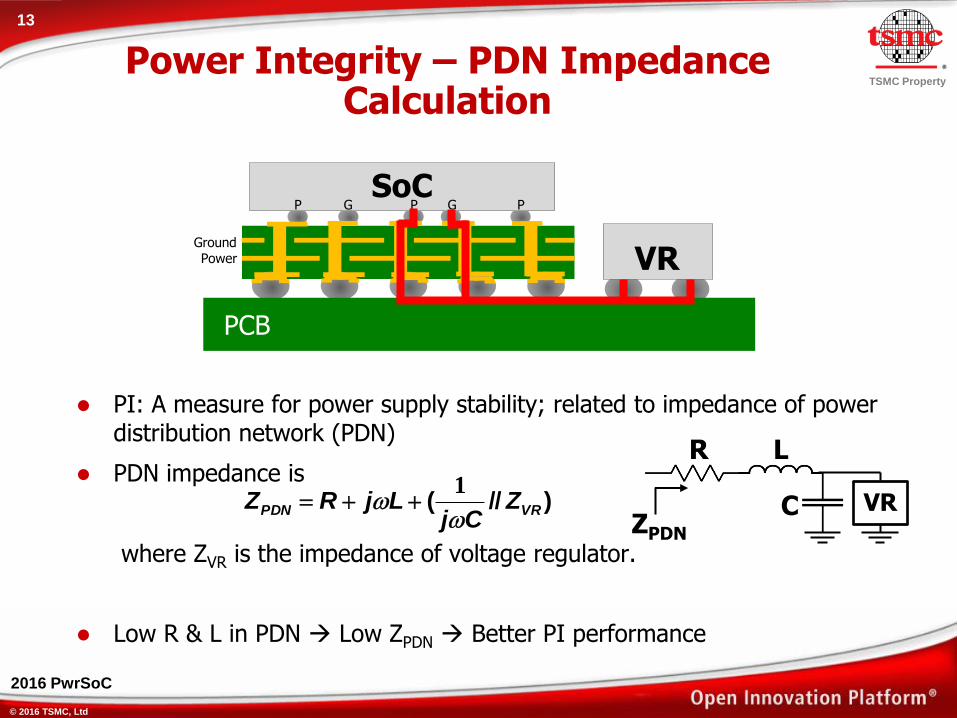
Power Integrity – PDN Impedance Calculation
PI: A measure for power supply stability; related to impedance of power distribution network (PDN)
PDN impedance is
where ZVR is the impedance of voltage regulator.
Low R & L in PDN Low ZPDN Better PI performance
VR
R L
C ZPDN
)//( VRPDN ZCj
LjRZ
1
SoC P G G P P
Power Ground
PCB
VR
© 2016 TSMC, Ltd
14
TSMC Property
2016 PwrSoC
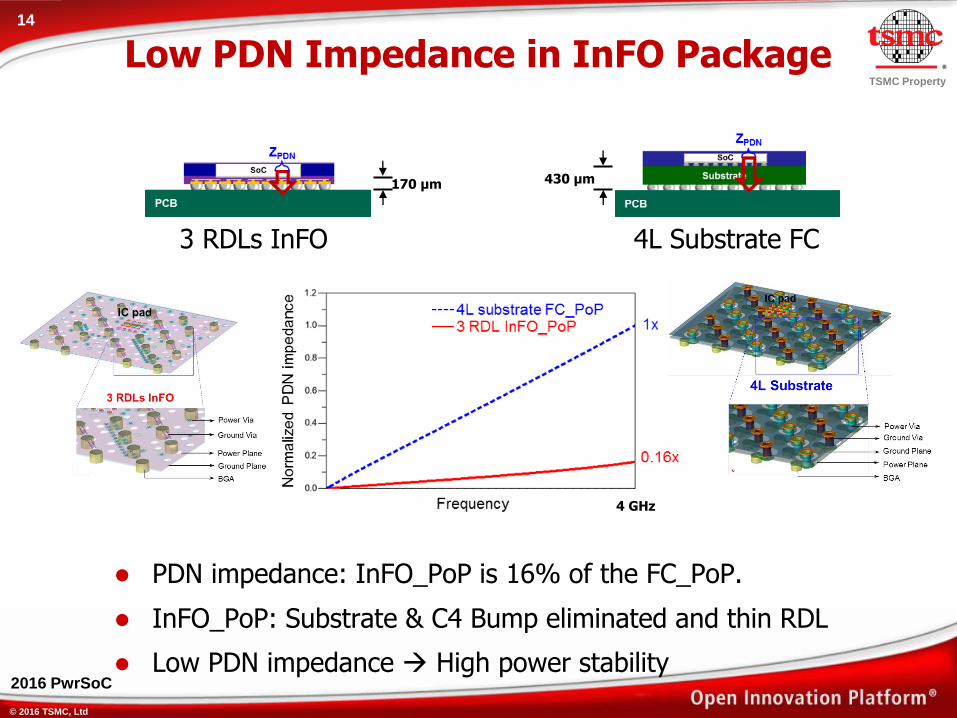
Low PDN Impedance in InFO Package
PDN impedance: InFO_PoP is 16% of the FC_PoP.
InFO_PoP: Substrate & C4 Bump eliminated and thin RDL
Low PDN impedance High power stability
4 GHz
170 μm 430 μm
3 RDLs InFO 4L Substrate FC
© 2016 TSMC, Ltd
15
TSMC Property
2016 PwrSoC
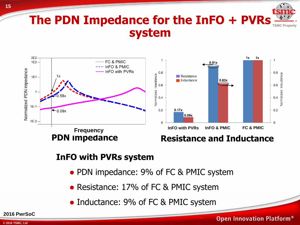
The PDN Impedance for the InFO + PVRs system
InFO with PVRs system
PDN impedance: 9% of FC & PMIC system
Resistance: 17% of FC & PMIC system
Inductance: 9% of FC & PMIC system
PDN impedance Resistance and Inductance Frequency
InFO with PVRs InFO & PMIC FC & PMIC
© 2016 TSMC, Ltd
16
TSMC Property
2016 PwrSoC
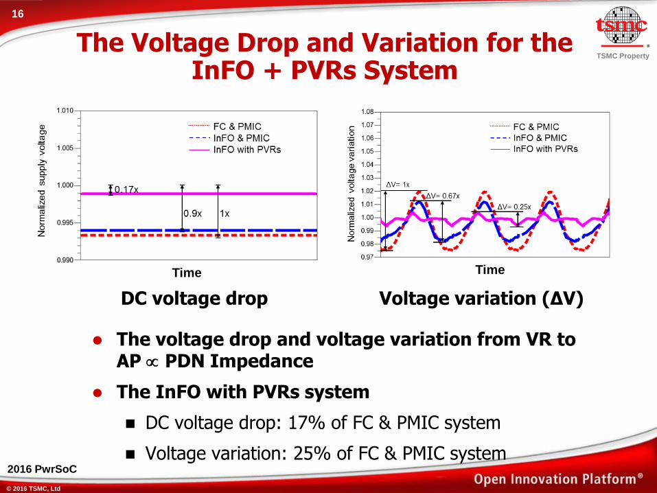
The Voltage Drop and Variation for the InFO + PVRs System
The voltage drop and voltage variation from VR to AP PDN Impedance
The InFO with PVRs system
DC voltage drop: 17% of FC & PMIC system
Voltage variation: 25% of FC & PMIC system
DC voltage drop Voltage variation (ΔV)
Time Time
© 2016 TSMC, Ltd
17
TSMC Property
2016 PwrSoC
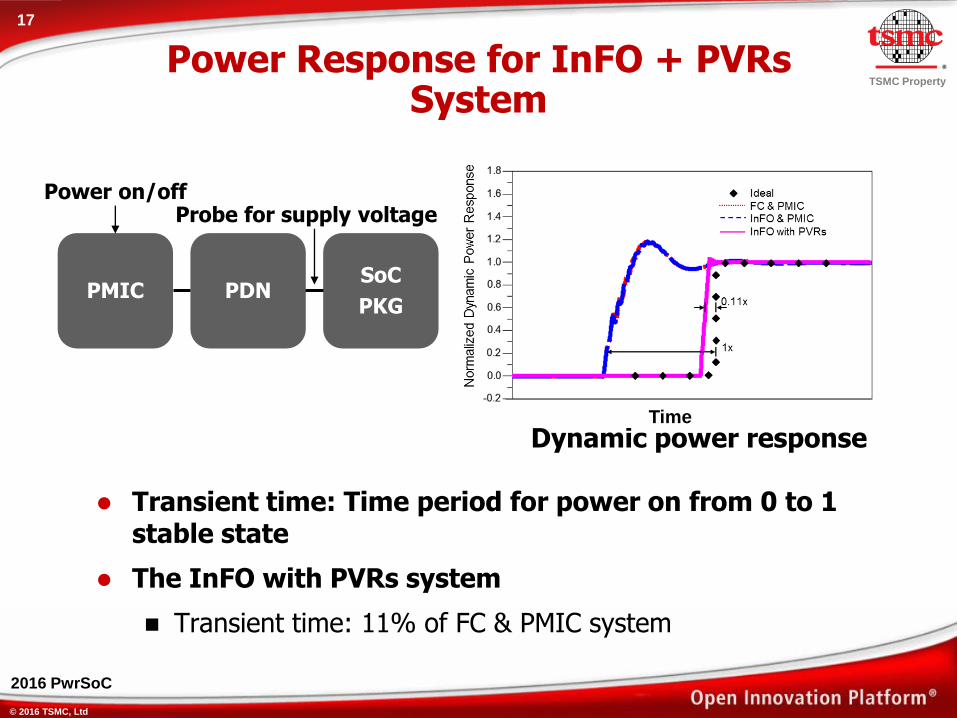
Power Response for InFO + PVRs System
Transient time: Time period for power on from 0 to 1 stable state
The InFO with PVRs system
Transient time: 11% of FC & PMIC system
Dynamic power response
SoC
PKG PMIC PDN
Probe for supply voltage Power on/off
Time
© 2016 TSMC, Ltd
18
TSMC Property
2016 PwrSoC
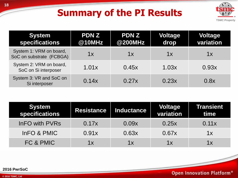
Summary of the PI Results
System
specifications Resistance Inductance
Voltage
variation Transient
time
InFO with PVRs 0.17x 0.09x 0.25x 0.11x
InFO & PMIC 0.91x 0.63x 0.67x 1x
FC & PMIC 1x 1x 1x 1x
System
specifications PDN Z
@10MHz PDN Z
@200MHz Voltage
drop Voltage
variation
System 1: VRM on board,
SoC on substrate (FCBGA) 1x 1x 1x 1x
System 2: VRM on board,
SoC on Si interposer 1.01x 0.45x 1.03x 0.93x
System 3: VR and SoC on
Si interposer 0.14x 0.27x 0.23x 0.8x
© 2016 TSMC, Ltd
19
TSMC Property
2016 PwrSoC
Summary and Outlooks
Foundry WLSI technology, CoWoS and InFO, provides leading edge solutions for power management system integration.
The technologies provide excellent PDN performance for low power consumption, low voltage drop and low voltage variation for system design.
Vdd scaling of SoC leads to power system design challenges TSMC WLSI technology provides the design solution.

© 2016 TSMC, Ltd
20
TSMC Property
2016 PwrSoC
Thanks for your attention!