floating gate techniques and applicationss-sanchez/607-2010-floating gate circuits.pdf · floating...
TRANSCRIPT
1
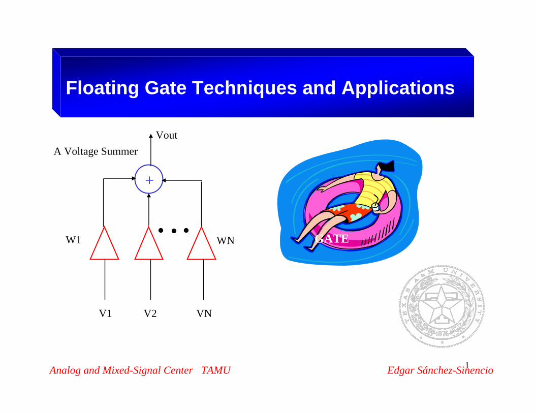
V1 V2 VN
+
Vout
W1 WN
Analog and Mixed-Signal Center TAMU Edgar Sánchez-Sinencio
Floating Gate Techniques and Applications
GATE
A Voltage Summer
2
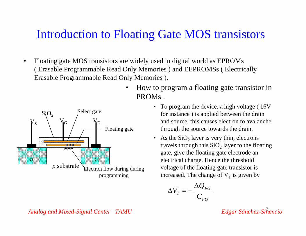
Introduction to Floating Gate MOS transistors
• Floating gate MOS transistors are widely used in digital world as EPROMs( Erasable Programmable Read Only Memories ) and EEPROMSs ( Electrically Erasable Programmable Read Only Memories ).
n+ n+p substrate
VS VG VD
Select gate
Floating gate
Electron flow during during programming
SiO2
• How to program a floating gate transistor in PROMs .
• To program the device, a high voltage ( 16V for instance ) is applied between the drain and source, this causes electron to avalanche through the source towards the drain.
• As the SiO2 layer is very thin, electrons travels through this SiO2 layer to the floating gate, give the floating gate electrode an electrical charge. Hence the threshold voltage of the floating gate transistor is increased. The change of VT is given by
FG
FGT C
QV Δ−=Δ
Analog and Mixed-Signal Center TAMU Edgar Sánchez-Sinencio
3
Multiple-Input Floating Gate MOS Transistors
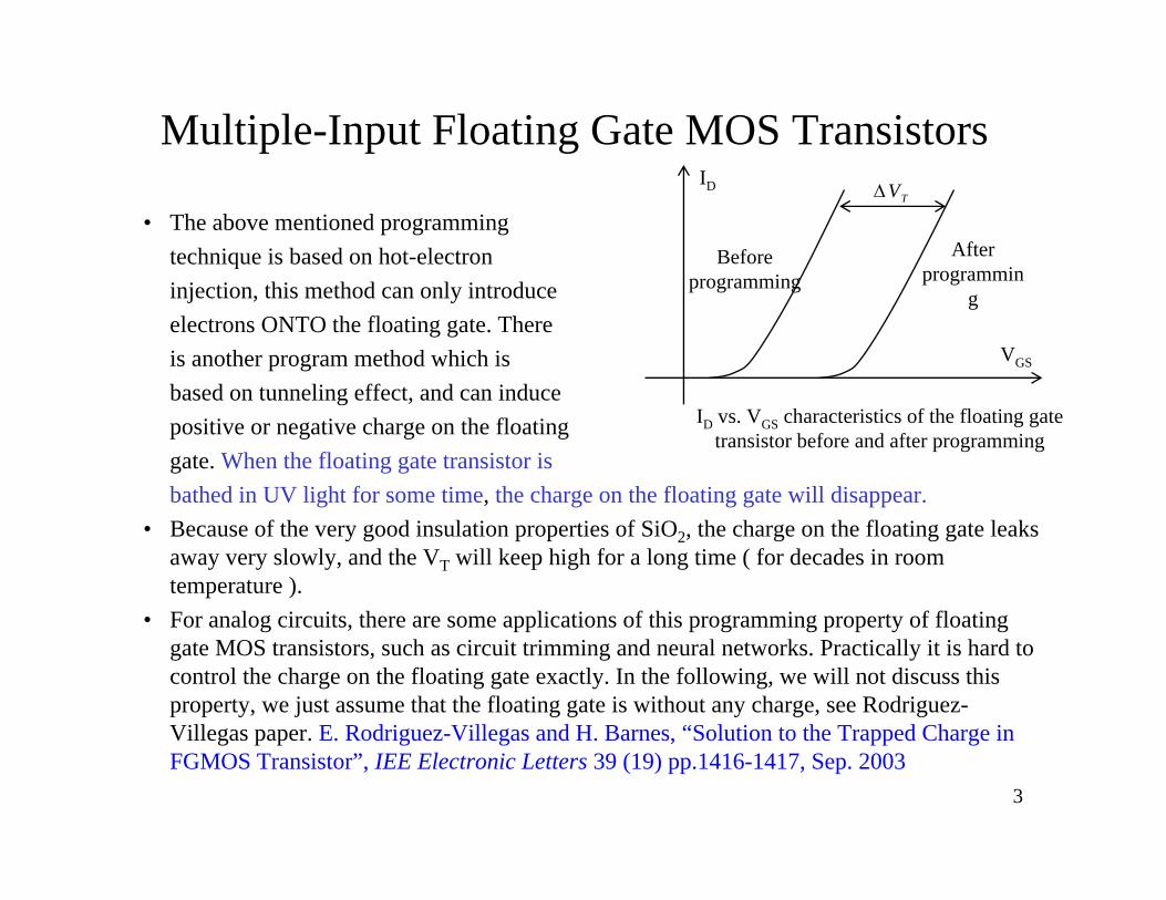
• The above mentioned programmingtechnique is based on hot-electroninjection, this method can only introduceelectrons ONTO the floating gate. Thereis another program method which isbased on tunneling effect, and can inducepositive or negative charge on the floatinggate. When the floating gate transistor isbathed in UV light for some time, the charge on the floating gate will disappear.
• Because of the very good insulation properties of SiO2, the charge on the floating gate leaks away very slowly, and the VT will keep high for a long time ( for decades in room temperature ).
• For analog circuits, there are some applications of this programming property of floating gate MOS transistors, such as circuit trimming and neural networks. Practically it is hard to control the charge on the floating gate exactly. In the following, we will not discuss this property, we just assume that the floating gate is without any charge, see Rodriguez-Villegas paper. E. Rodriguez-Villegas and H. Barnes, “Solution to the Trapped Charge in FGMOS Transistor”, IEE Electronic Letters 39 (19) pp.1416-1417, Sep. 2003
After programmin
g
TVΔ
VGS
ID
ID vs. VGS characteristics of the floating gate transistor before and after programming
Before programming
4
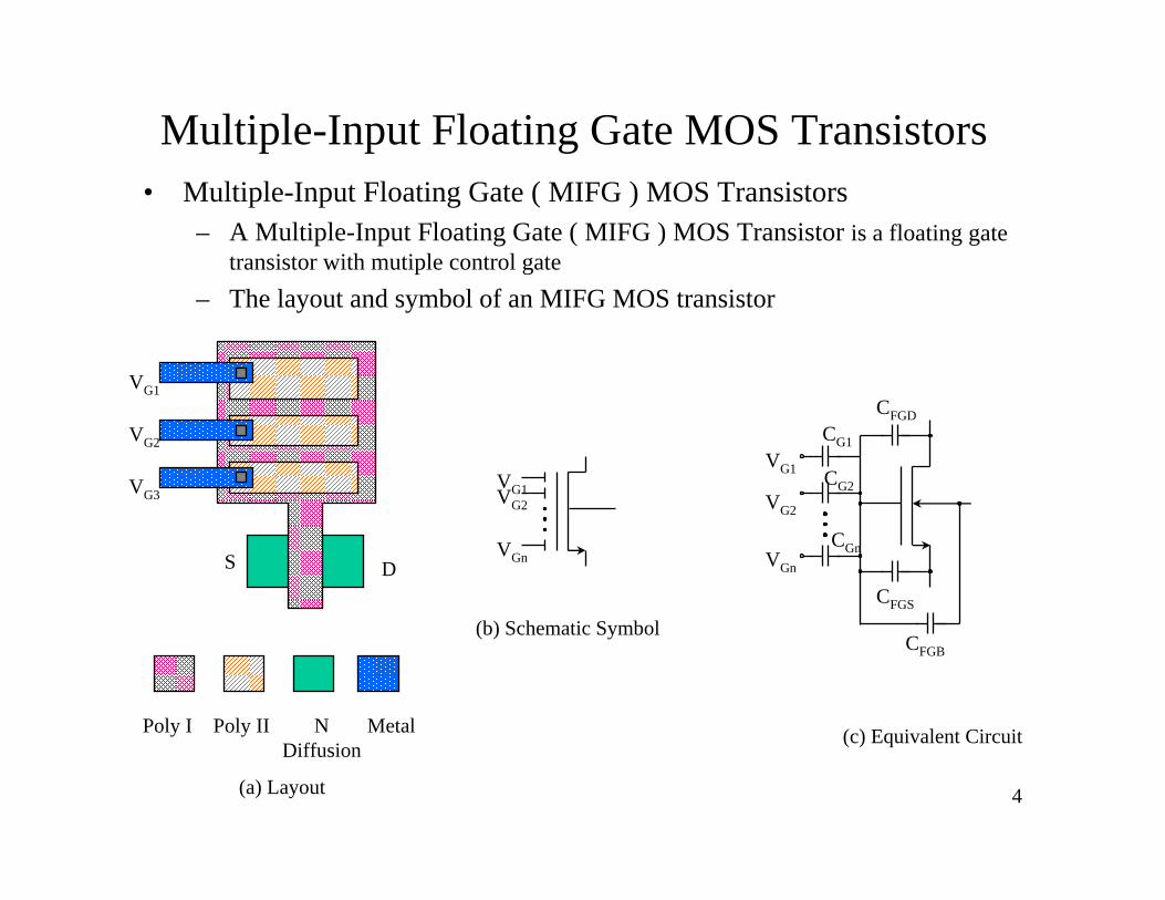
Multiple-Input Floating Gate MOS Transistors• Multiple-Input Floating Gate ( MIFG ) MOS Transistors
– A Multiple-Input Floating Gate ( MIFG ) MOS Transistor is a floating gate transistor with mutiple control gate
– The layout and symbol of an MIFG MOS transistor
Poly I Poly II N Diffusion
Metal
VG1VG2
VGn
VG1
VG2
VG3
S D
VG1
VG2
VGn
CG1
CG2
CGn
CFGB
CFGS
CFGD
(a) Layout
(b) Schematic Symbol
(c) Equivalent Circuit
5
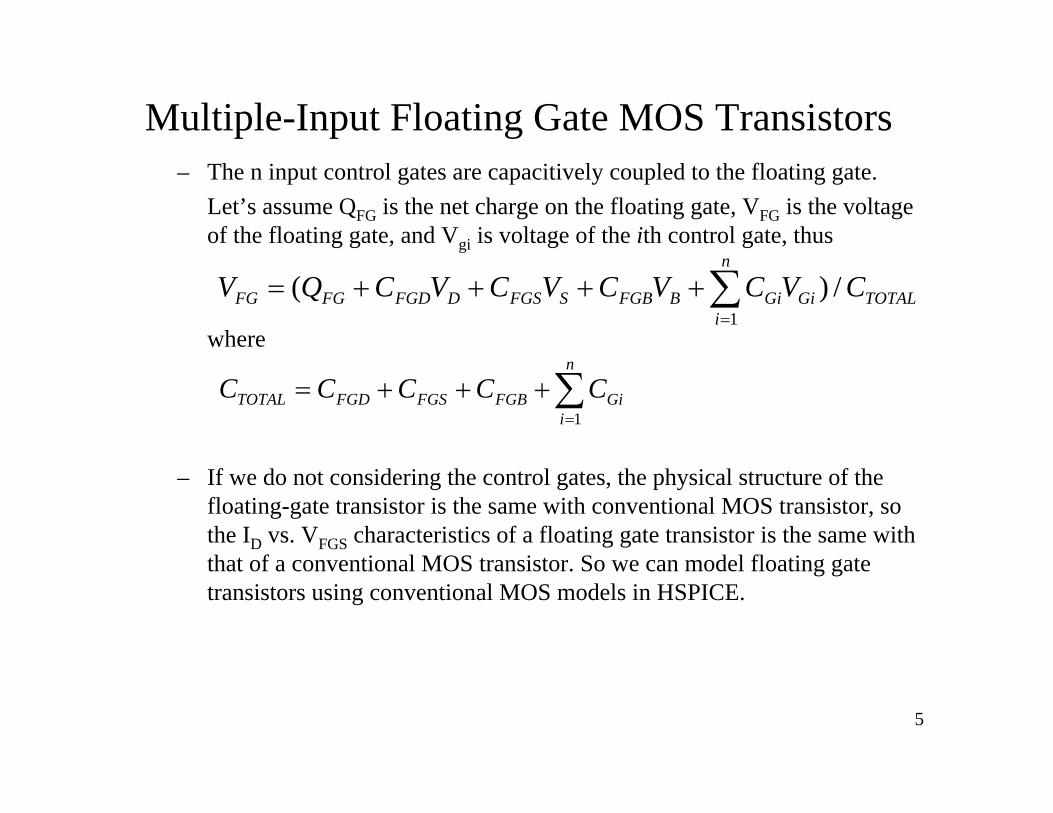
Multiple-Input Floating Gate MOS Transistors– The n input control gates are capacitively coupled to the floating gate.
Let’s assume QFG is the net charge on the floating gate, VFG is the voltage of the floating gate, and Vgi is voltage of the ith control gate, thus
where
– If we do not considering the control gates, the physical structure of the floating-gate transistor is the same with conventional MOS transistor, sothe ID vs. VFGS characteristics of a floating gate transistor is the same with that of a conventional MOS transistor. So we can model floating gate transistors using conventional MOS models in HSPICE.
∑=
+++=n
iGiFGBFGSFGDTOTAL CCCCC
1
∑=
++++=n
iTOTALGiGiBFGBSFGSDFGDFGFG CVCVCVCVCQV
1/)(
6
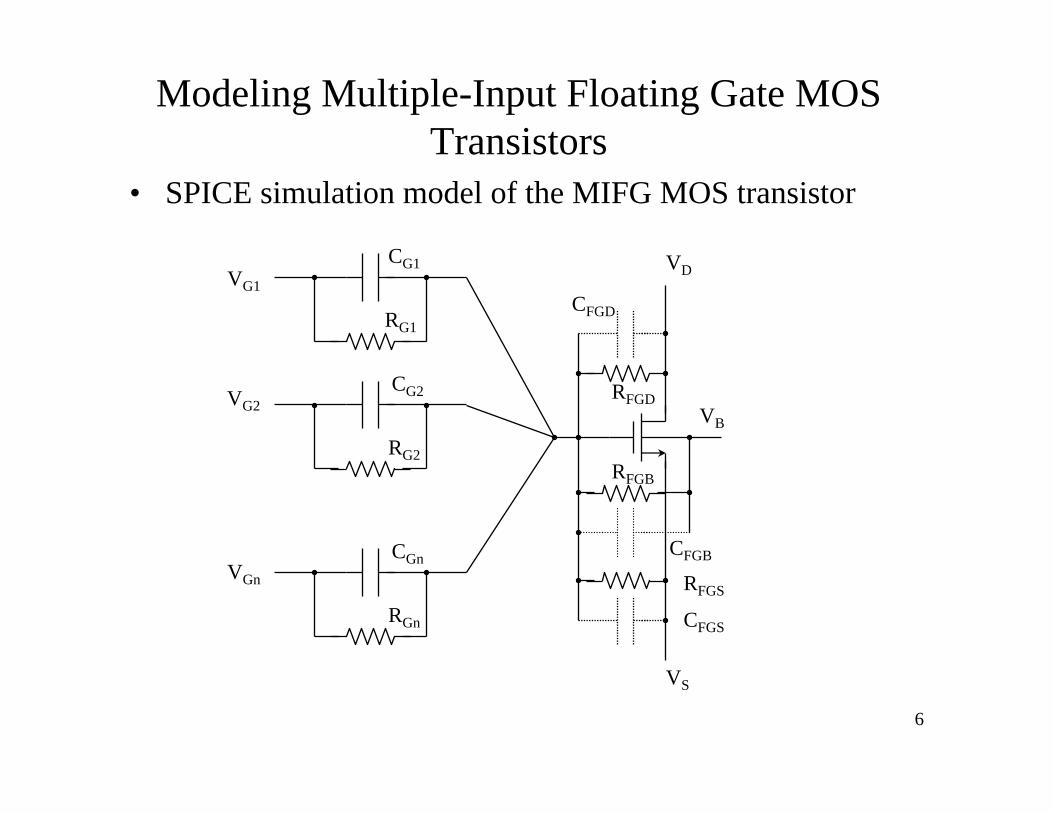
Modeling Multiple-Input Floating Gate MOS Transistors
• SPICE simulation model of the MIFG MOS transistor
VG1
VG2
VGn
RG1
CG1
RG2
CG2
RGn
CGn
RFGD
RFGS
RFGB
CFGS
CFGD
CFGB
VS
VD
VB
7
Modeling Multiple-Input Floating Gate MOS Transistors
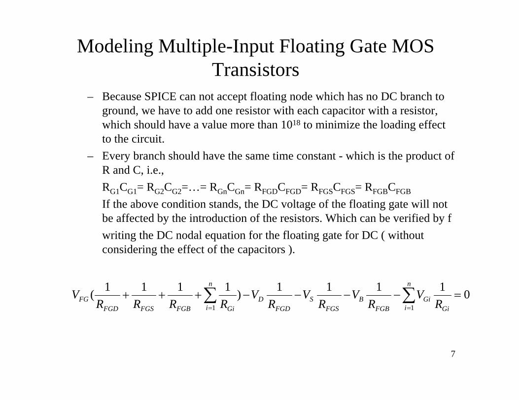
– Because SPICE can not accept floating node which has no DC branch to ground, we have to add one resistor with each capacitor with a resistor, which should have a value more than 1018 to minimize the loading effect to the circuit.
– Every branch should have the same time constant - which is the product of R and C, i.e.,RG1CG1= RG2CG2=…= RGnCGn= RFGDCFGD= RFGSCFGS= RFGBCFGB
If the above condition stands, the DC voltage of the floating gate will not be affected by the introduction of the resistors. Which can be verified by fwriting the DC nodal equation for the floating gate for DC ( without considering the effect of the capacitors ).
01111)1111(11
=−−−−+++ ∑∑==
n
i GiGi
FGBB
FGSS
FGDD
n
i GiFGBFGSFGDFG R
VR
VR
VR
VRRRR
V
8
Modeling Multiple-Input Floating Gate MOS Transistors
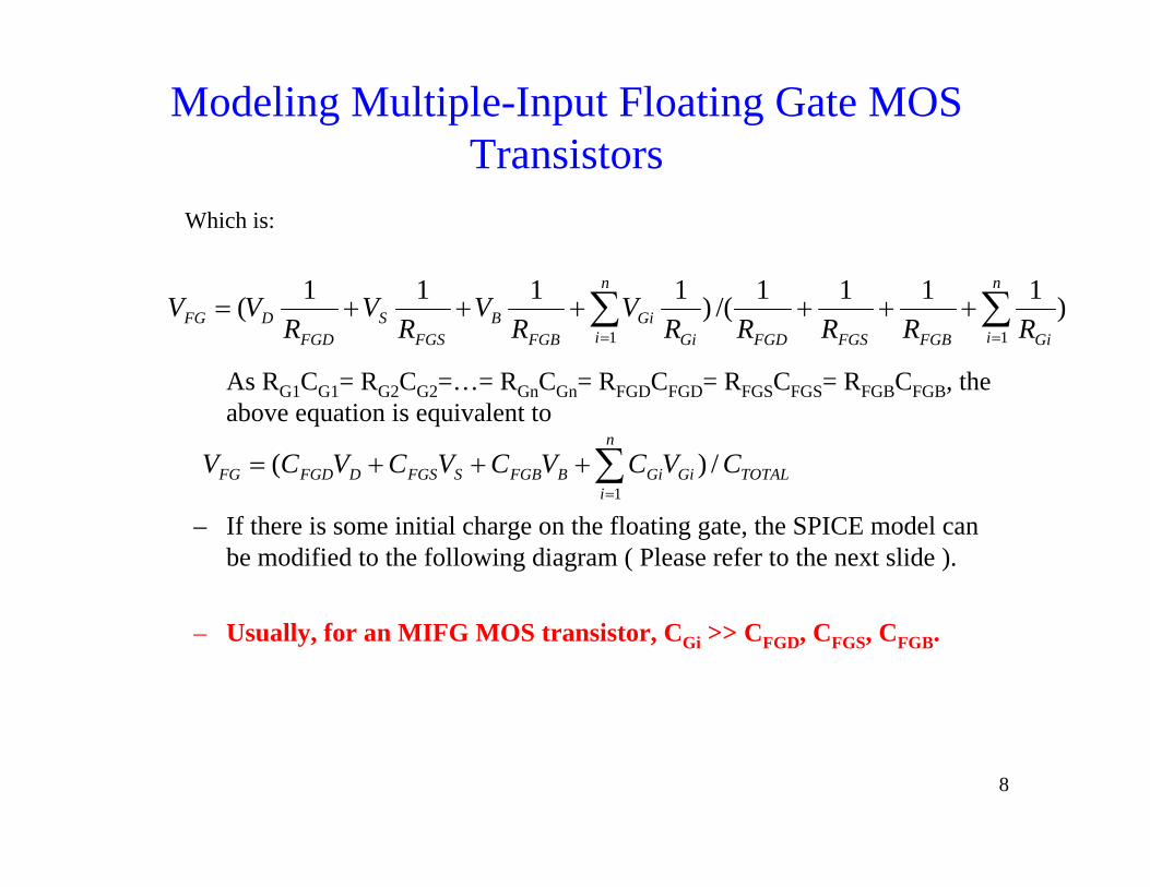
As RG1CG1= RG2CG2=…= RGnCGn= RFGDCFGD= RFGSCFGS= RFGBCFGB, the above equation is equivalent to
– If there is some initial charge on the floating gate, the SPICE model can be modified to the following diagram ( Please refer to the next slide ).
– Usually, for an MIFG MOS transistor, CGi >> CFGD, CFGS, CFGB.
)1111/()1111(11∑∑==
++++++=n
i GiFGBFGSFGD
n
i GiGi
FGBB
FGSS
FGDDFG RRRRR
VR
VR
VR
VV
∑=
+++=n
iTOTALGiGiBFGBSFGSDFGDFG CVCVCVCVCV
1/)(
Which is:
9
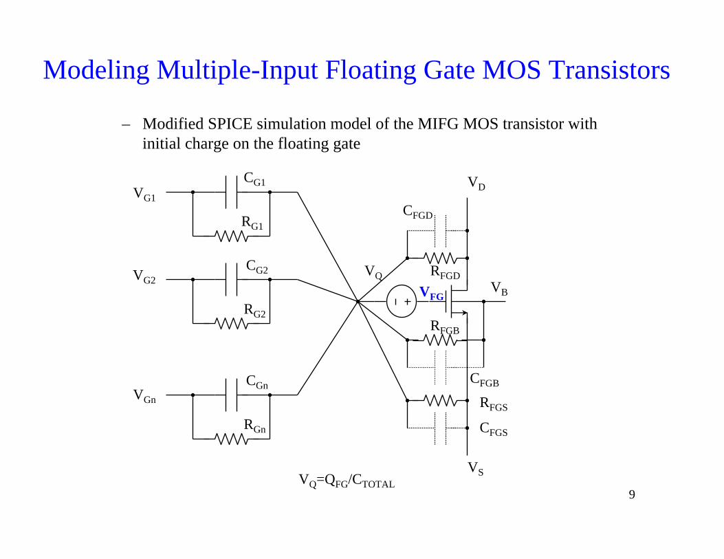
Modeling Multiple-Input Floating Gate MOS Transistors
– Modified SPICE simulation model of the MIFG MOS transistor with initial charge on the floating gate
VG1
VG2
VGn
RG1
CG1
RG2
CG2
RGn
CGn
RFGD
RFGS
RFGB
CFGS
CFGD
CFGB
VS
VD
VBVFG
VQ
VQ=QFG/CTOTAL
10
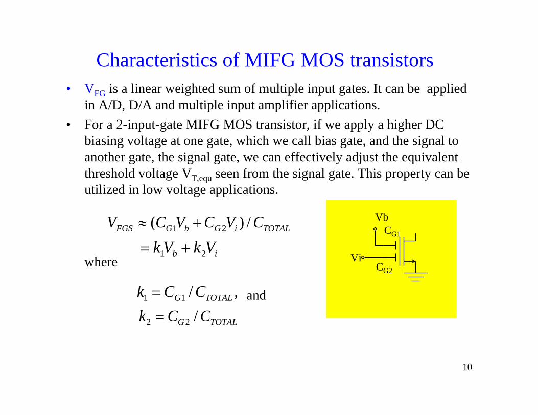
Characteristics of MIFG MOS transistors• VFG is a linear weighted sum of multiple input gates. It can be applied
in A/D, D/A and multiple input amplifier applications.• For a 2-input-gate MIFG MOS transistor, if we apply a higher DC
biasing voltage at one gate, which we call bias gate, and the signal to another gate, the signal gate, we can effectively adjust the equivalent threshold voltage VT,equ seen from the signal gate. This property can be utilized in low voltage applications.
where
Vb
Vi
CG1
CG2
TOTALiGbGFGS CVCVCV /)( 21 +≈
ib VkVk 21 +=
,/11 TOTALG CCk =
TOTALG CCk /22 =and
11
Characteristics of MIFG MOS Transistors• The equivalent threshold voltage seen from Vi is given by
which may less than VT depending on the value of Vb, k1 and k2.
• The effective transconductance is given by
where gm,FG is the transconductance seen from the floating gate.Note that gm,eff is less than gm,FG by a factor of k1.
• The output impedanceAs there is a DC and AC feedback from drain to floating gate through CGD, the output impedance is less than that of an MOS transistor working in the same biasing condition.
2
1, k
kVVV bTequT
−=
FGmeffm gkg ,2, =
12
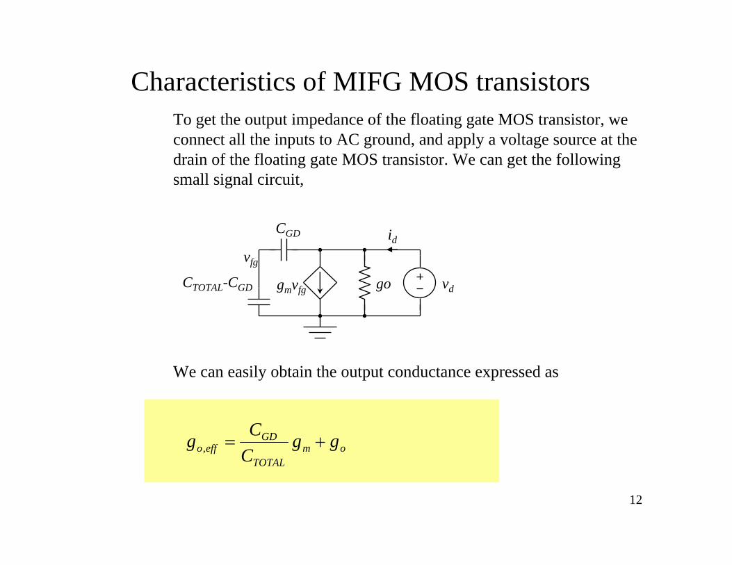
Characteristics of MIFG MOS transistorsTo get the output impedance of the floating gate MOS transistor, we connect all the inputs to AC ground, and apply a voltage source at the drain of the floating gate MOS transistor. We can get the following small signal circuit,
We can easily obtain the output conductance expressed as
vd
idCGD
CTOTAL-CGD
vfg
gmvfg go
omTOTAL
GDeffo gg
CCg +=,
13
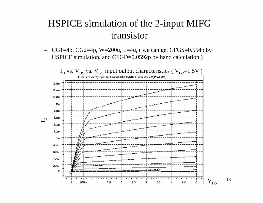
HSPICE simulation of the 2-input MIFG transistor
– CG1=4p, CG2=4p, W=200u, L=4u, ( we can get CFGS=0.554p by HSPICE simulation, and CFGD=0.0592p by hand calculation )
VDS
I D
ID vs. VDS vs. VGS input output characteristics ( VG2=1.5V )
14
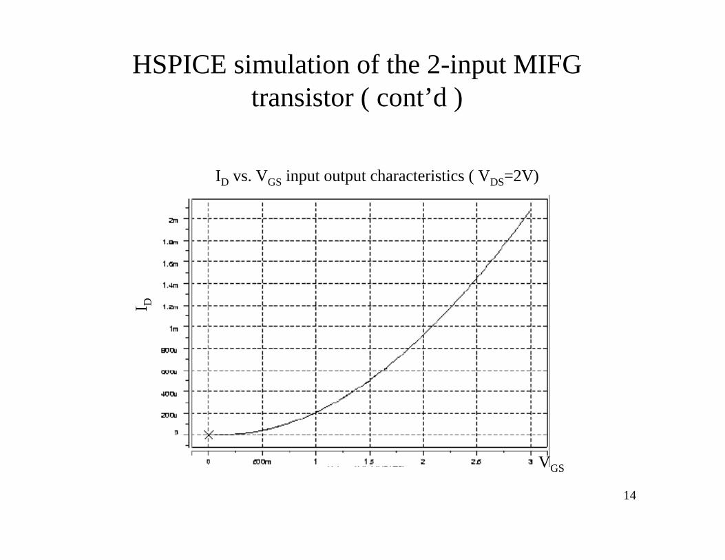
HSPICE simulation of the 2-input MIFG transistor ( cont’d )I D
VGS
ID vs. VGS input output characteristics ( VDS=2V)
15
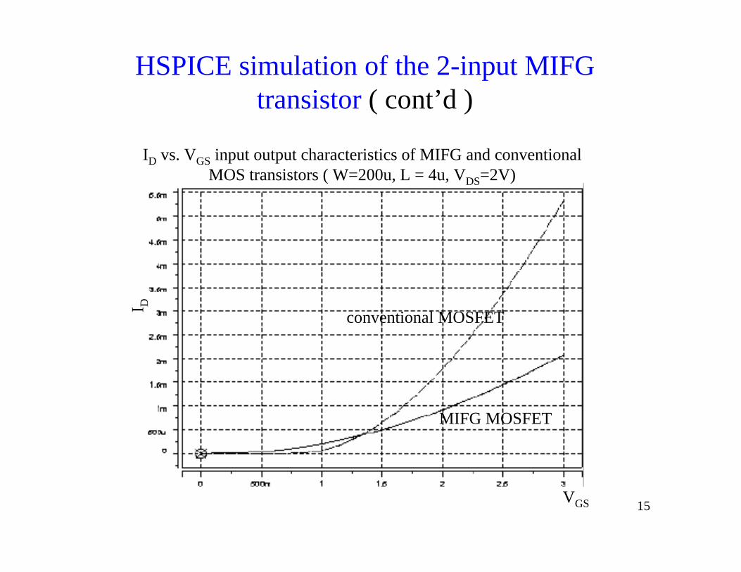
HSPICE simulation of the 2-input MIFG transistor ( cont’d )
VGS
ID vs. VGS input output characteristics of MIFG and conventional MOS transistors ( W=200u, L = 4u, VDS=2V)
I D
MIFG MOSFET
conventional MOSFET
16
HSPICE simulation of the 2-input MIFG transistor ( cont’d )
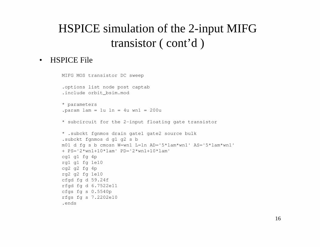
• HSPICE File
MIFG MOS transistor DC sweep
.options list node post captab
.include orbit_bsim.mod
* parameters.param lam = 1u ln = 4u wn1 = 200u
* subcircuit for the 2-input floating gate transistor
* .subckt fgnmos drain gate1 gate2 source bulk.subckt fgnmos d g1 g2 s bm01 d fg s b cmosn W=wn1 L=ln AD='5*lam*wn1' AS='5*lam*wn1'+ PS='2*wn1+10*lam' PD='2*wn1+10*lam'cg1 g1 fg 4prg1 g1 fg 1e10cg2 g2 fg 4prg2 g2 fg 1e10cfgd fg d 59.24frfgd fg d 6.7522e11cfgs fg s 0.5540p rfgs fg s 7.2202e10.ends
17
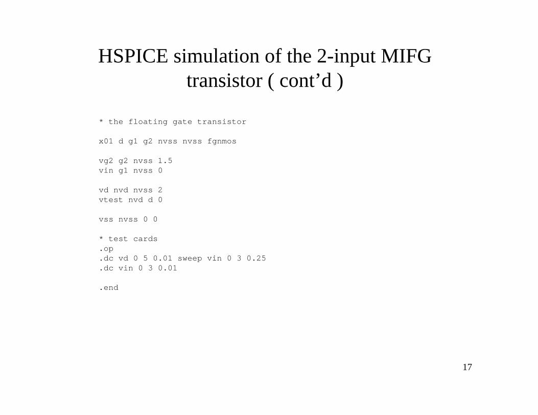
HSPICE simulation of the 2-input MIFG transistor ( cont’d )
* the floating gate transistor
x01 d g1 g2 nvss nvss fgnmos
vg2 g2 nvss 1.5vin g1 nvss 0
vd nvd nvss 2vtest nvd d 0
vss nvss 0 0
* test cards.op.dc vd 0 5 0.01 sweep vin 0 3 0.25.dc vin 0 3 0.01
.end
18
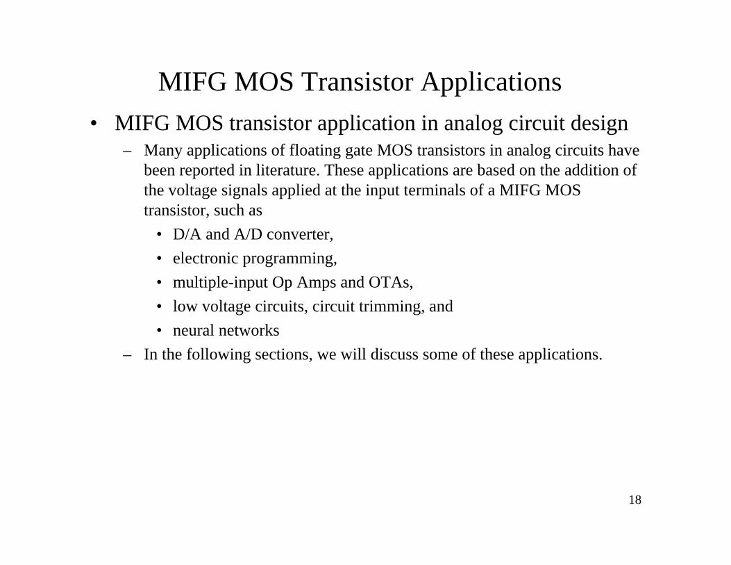
MIFG MOS Transistor Applications• MIFG MOS transistor application in analog circuit design
– Many applications of floating gate MOS transistors in analog circuits have been reported in literature. These applications are based on the addition of the voltage signals applied at the input terminals of a MIFG MOStransistor, such as
• D/A and A/D converter,• electronic programming,• multiple-input Op Amps and OTAs,• low voltage circuits, circuit trimming, and• neural networks
– In the following sections, we will discuss some of these applications.
19
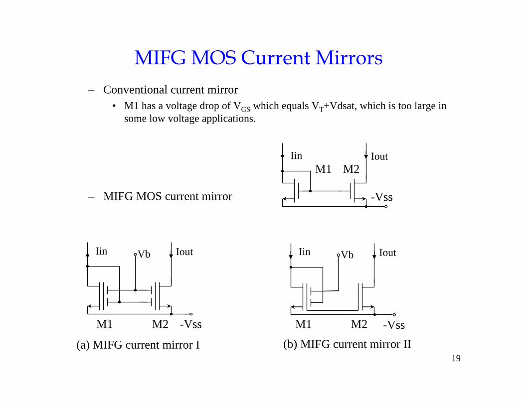
MIFG MOS Current Mirrors– Conventional current mirror
• M1 has a voltage drop of VGS which equals VT+Vdsat, which is too large in some low voltage applications.
– MIFG MOS current mirror
M1
-Vss
M2Iin Iout
-Vss
VbIin Iout
(a) MIFG current mirror I
-Vss
VbIin Iout
(b) MIFG current mirror II
M1 M2 M1 M2

20
MIFG MOS Current Mirrors• MIFG current mirror I is easy to understand.• The layout for the MIFG current mirror II is shown below, it is more
compact than I
Poly I Poly II NDiffusion Metal
Vb
Vb
M1
M2
S
S
D
DM1 M2
Vb
Vi
CG1
CG2
CFGB1 CFGB2
CFGS1
CFGD1 CFGD2
CFGS2
M1 M2
(a) Layout
(b) Schematic Symbol(c) Equivalent Circuit
Vi
Vi
21
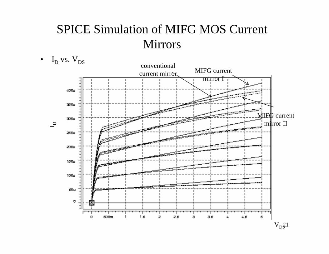
SPICE Simulation of MIFG MOS Current Mirrors
• ID vs. VDS
VDS
I D
MIFG current mirror I
MIFG current mirror II
conventional current mirror
22
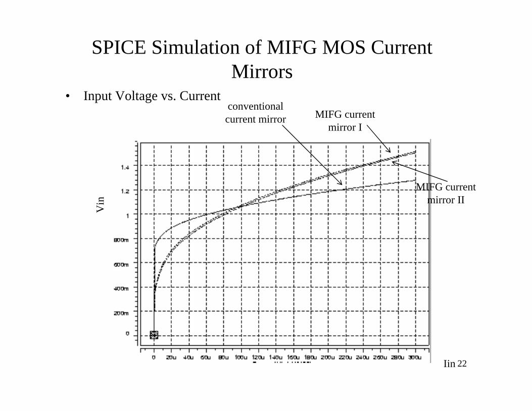
SPICE Simulation of MIFG MOS Current Mirrors
• Input Voltage vs. Current
Iin
Vin
MIFG current mirror I
MIFG current mirror II
conventional current mirror
23
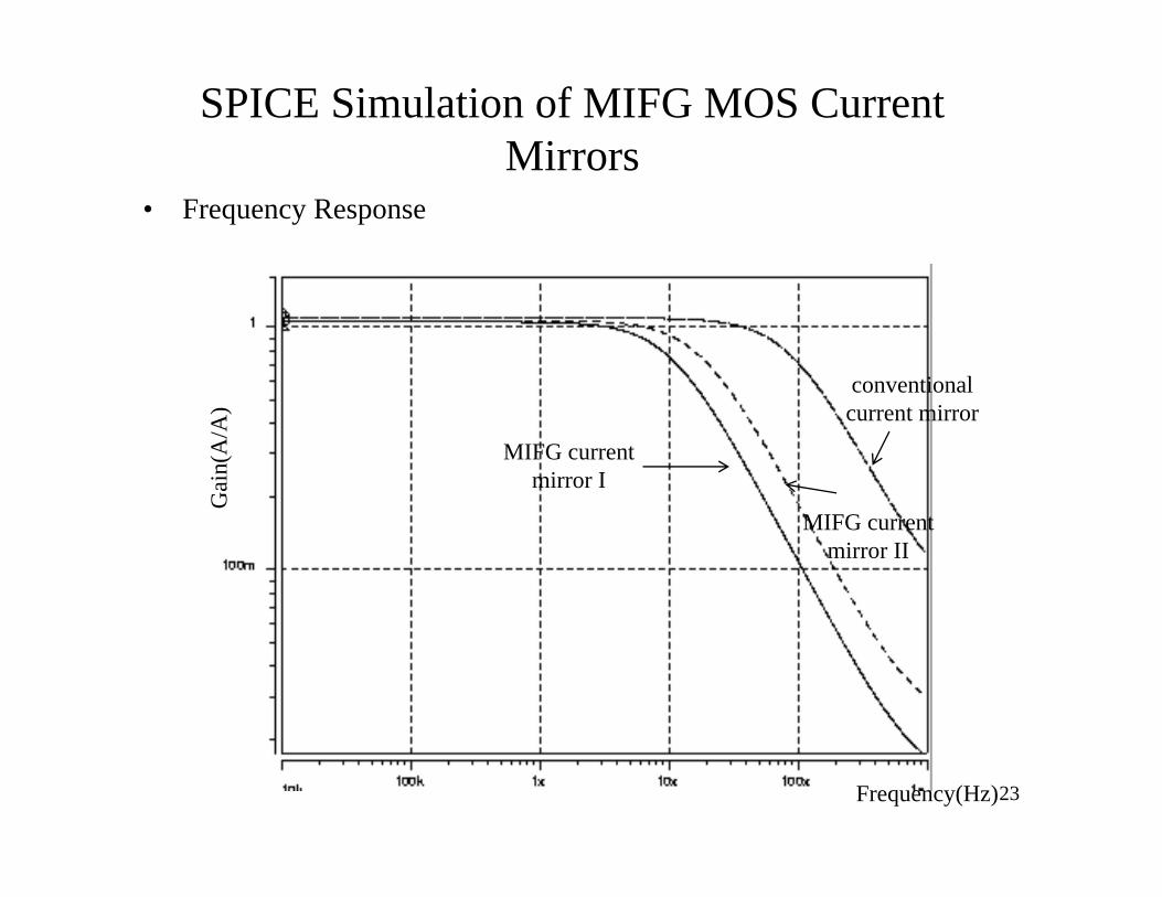
SPICE Simulation of MIFG MOS Current Mirrors
• Frequency Response
Frequency(Hz)
Gai
n(A
/A)
MIFG current mirror I
MIFG current mirror II
conventional current mirror
24
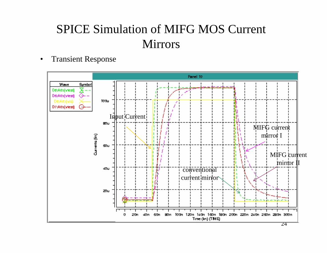
SPICE Simulation of MIFG MOS Current Mirrors
• Transient Response
MIFG current mirror I
MIFG current mirror II
conventional current mirror
Input Current
25
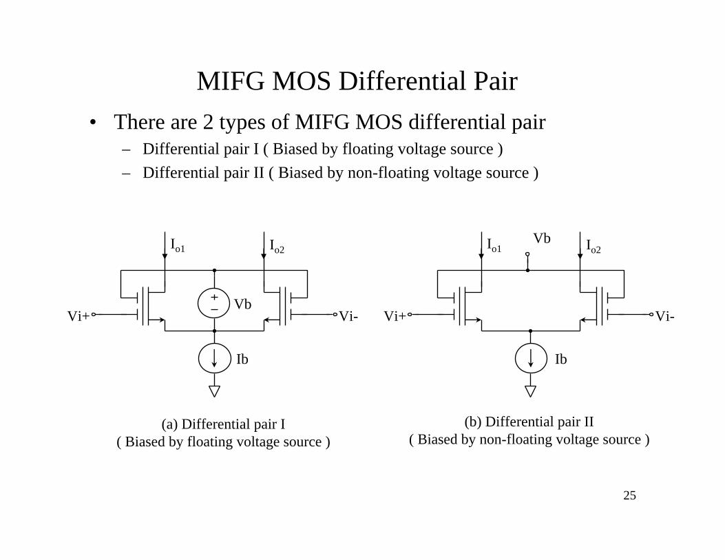
MIFG MOS Differential Pair• There are 2 types of MIFG MOS differential pair
– Differential pair I ( Biased by floating voltage source )– Differential pair II ( Biased by non-floating voltage source )
Vi+ Vi-
Io1 Io2
Vi+ Vi-
Io1 Io2Vb
Vb
Ib Ib
(a) Differential pair I( Biased by floating voltage source )
(b) Differential pair II( Biased by non-floating voltage source )
26
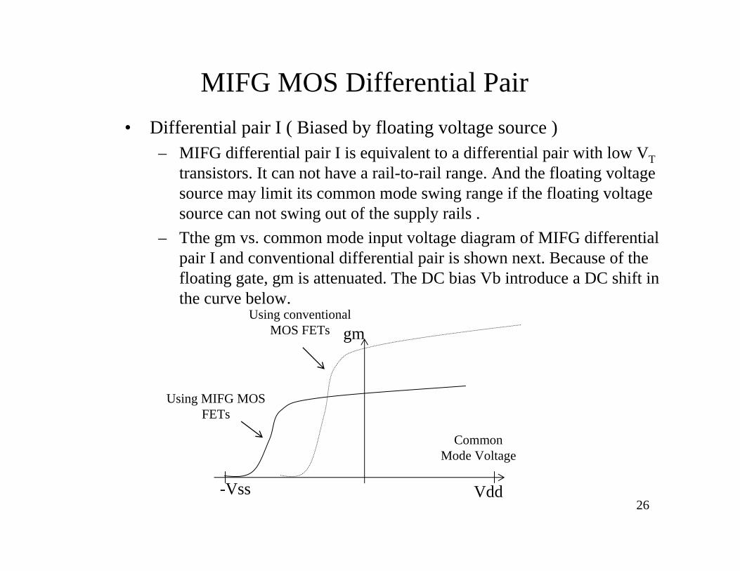
MIFG MOS Differential Pair• Differential pair I ( Biased by floating voltage source )
– MIFG differential pair I is equivalent to a differential pair with low VTtransistors. It can not have a rail-to-rail range. And the floating voltage source may limit its common mode swing range if the floating voltage source can not swing out of the supply rails .
– Tthe gm vs. common mode input voltage diagram of MIFG differential pair I and conventional differential pair is shown next. Because of the floating gate, gm is attenuated. The DC bias Vb introduce a DC shift in the curve below.
Common Mode Voltage
-Vss Vdd
gmUsing conventional
MOS FETs
Using MIFG MOS FETs
27
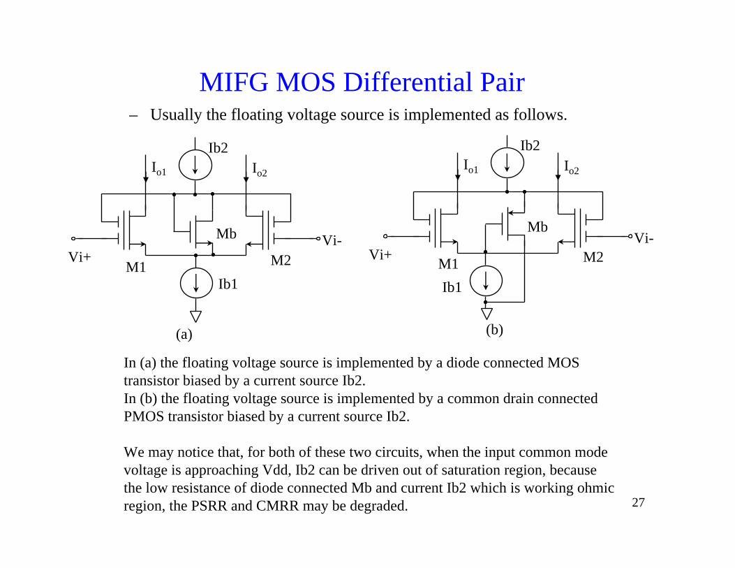
MIFG MOS Differential Pair– Usually the floating voltage source is implemented as follows.
In (a) the floating voltage source is implemented by a diode connected MOS transistor biased by a current source Ib2.In (b) the floating voltage source is implemented by a common drain connected PMOS transistor biased by a current source Ib2.
We may notice that, for both of these two circuits, when the input common mode voltage is approaching Vdd, Ib2 can be driven out of saturation region, because the low resistance of diode connected Mb and current Ib2 which is working ohmic region, the PSRR and CMRR may be degraded.
Vi-
Io1 Io2
Ib1
Ib2
Vi-
Io1 Io2
Ib1
Ib2
M1 M2 M1 M2Mb Mb
(a) (b)
Vi+Vi+

28
MIFG MOS Differential Pair• Differential Pair II ( Biased by non-floating voltage source )
In the following, we will derive under what condition we can get a rail-to-rail input common mode range for the Differential Pair II
– We know that for 2-input floating gate transistorsVF=w0V0+w1V1+w2V2
wherewi=Ci/CTOT, i = 0, 1, 2
Normally, Ci ( i = 1,2 ) is much larger thanC0, which means w0 is very small and wecan get the following approximation
w1+w2 = 1– When Vicm ( common mode input voltage ) is
Vdd, for N type transistor, the floating gate canbe Vdd, as long as the VDRAIN is greater thanVDD-VTN. So, for the diagram of DifferentialPair II shown in previous slides, Vb can directlybe Vdd.
(a) Layout
Poly II NDiffusion Metal
S D
29
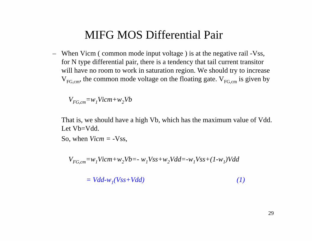
MIFG MOS Differential Pair– When Vicm ( common mode input voltage ) is at the negative rail -Vss,
for N type differential pair, there is a tendency that tail current transitorwill have no room to work in saturation region. We should try to increase VFG,cm, the common mode voltage on the floating gate. VFG,cm is given by
VFG,cm=w1Vicm+w2Vb
That is, we should have a high Vb, which has the maximum value of Vdd. Let Vb=Vdd.So, when Vicm = -Vss,
VFG,cm=w1Vicm+w2Vb=- w1Vss+w2Vdd=-w1Vss+(1-w1)Vdd
= Vdd-w1(Vss+Vdd) (1)
30
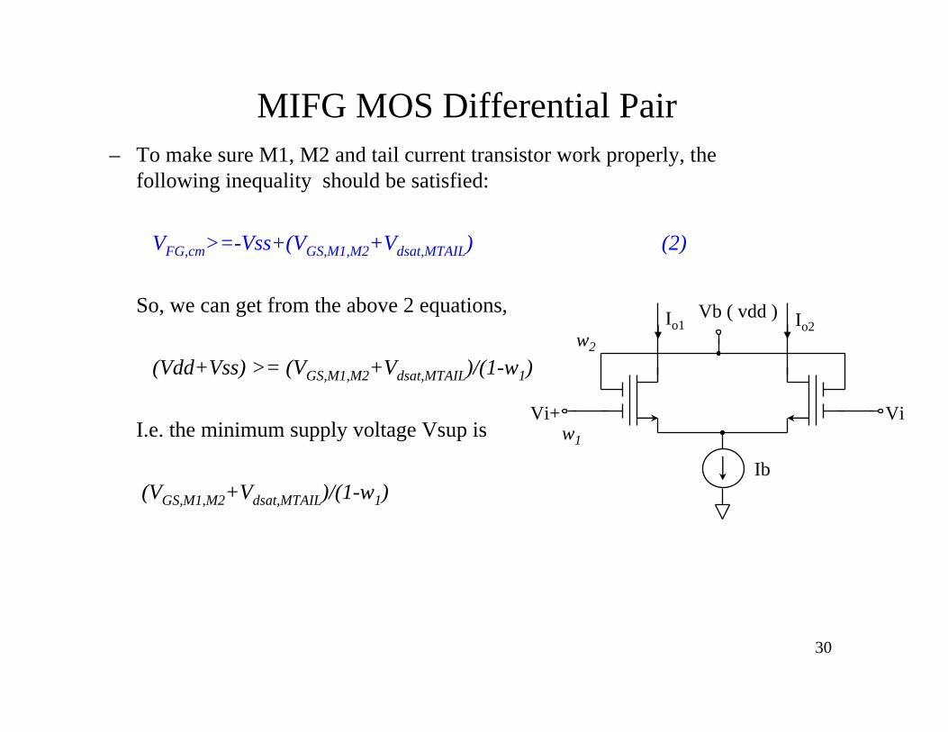
MIFG MOS Differential Pair– To make sure M1, M2 and tail current transistor work properly, the
following inequality should be satisfied:
VFG,cm>=-Vss+(VGS,M1,M2+Vdsat,MTAIL) (2)
So, we can get from the above 2 equations,
(Vdd+Vss) >= (VGS,M1,M2+Vdsat,MTAIL)/(1-w1)
I.e. the minimum supply voltage Vsup is
(VGS,M1,M2+Vdsat,MTAIL)/(1-w1)
Vi+ Vi
Io1 Io2Vb ( vdd )
Ib
w1
w2
31
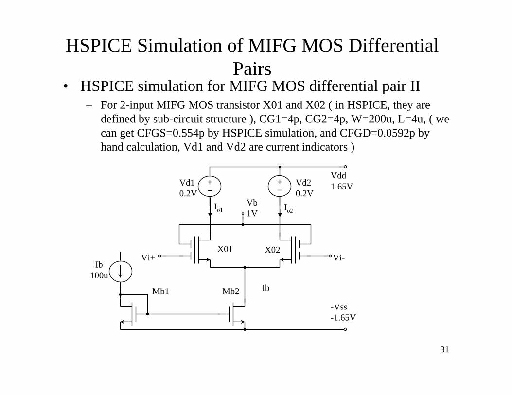
HSPICE Simulation of MIFG MOS Differential Pairs
• HSPICE simulation for MIFG MOS differential pair II– For 2-input MIFG MOS transistor X01 and X02 ( in HSPICE, they are
defined by sub-circuit structure ), CG1=4p, CG2=4p, W=200u, L=4u, ( we can get CFGS=0.554p by HSPICE simulation, and CFGD=0.0592p by hand calculation, Vd1 and Vd2 are current indicators )
Vi+ Vi-
Io1 Io2Vb1V
IbMb1
-Vss-1.65V
Mb2
Vd10.2V
Vd20.2V
Vdd1.65V
X01 X02Ib
100u
32
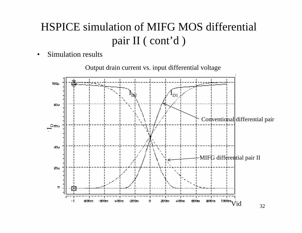
HSPICE simulation of MIFG MOS differential pair II ( cont’d )
• Simulation results
Output drain current vs. input differential voltage
Vid
I D
ID2 ID1
Conventional differential pair
MIFG differential pair II
33
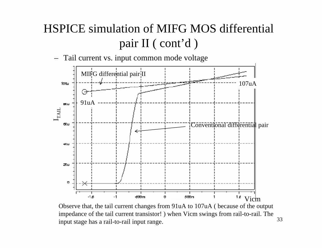
HSPICE simulation of MIFG MOS differential pair II ( cont’d )
– Tail current vs. input common mode voltage
Vicm
I TAIL
Observe that, the tail current changes from 91uA to 107uA ( because of the output impedance of the tail current transistor! ) when Vicm swings from rail-to-rail. The input stage has a rail-to-rail input range.
Conventional differential pair
MIFG differential pair II
91uA
107uA
34
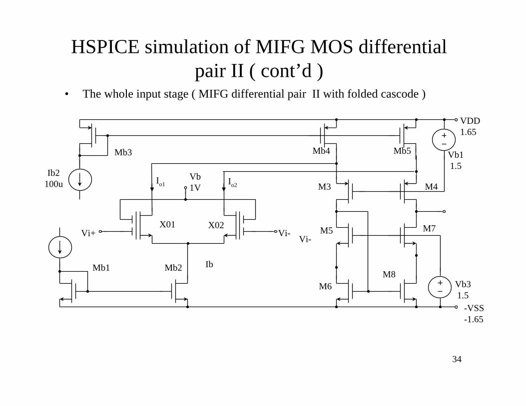
HSPICE simulation of MIFG MOS differential pair II ( cont’d )
Vi+ Vi-
Io1 Io2Vb1V
IbMb1 Mb2
X01 X02Vi-
M5 M7
M4M3
M6M8
Vb11.5
Vb31.5
VDD1.65
-VSS-1.65
Mb4 Mb5Mb3
Ib2100u
• The whole input stage ( MIFG differential pair II with folded cascode )
35
HSPICE simulation of MIFG MOS differential pair II ( cont’d )
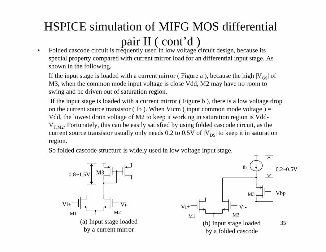
• Folded cascode circuit is frequently used in low voltage circuit design, because its special property compared with current mirror load for an differential input stage. As shown in the following.If the input stage is loaded with a current mirror ( Figure a ), because the high |VGS| of M3, when the common mode input voltage is close Vdd, M2 may have no room to swing and be driven out of saturation region.If the input stage is loaded with a current mirror ( Figure b ), there is a low voltage drop
on the current source transistor ( Ib ). When Vicm ( input common mode voltage ) = Vdd, the lowest drain voltage of M2 to keep it working in saturation region is Vdd-VT,M2. Fortunately, this can be easily satisfied by using folded cascode circuit, as the current source transistor usually only needs 0.2 to 0.5V of |VDS| to keep it in saturation region.So folded cascode structure is widely used in low voltage input stage.
Vi-M2
Vi+M1
M30.8~1.5V
M3
Ib
Vi-M2
Vi+M1
0.2~0.5V
(a) Input stage loaded by a current mirror
(b) Input stage loaded by a folded cascode
Vbp
36
HSPICE simulation of MIFG MOS differential pair II ( cont’d )
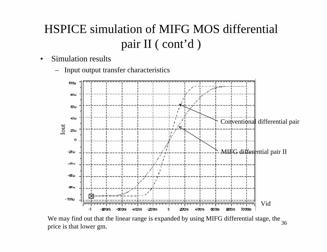
• Simulation results– Input output transfer characteristics
Vid
Iout
Conventional differential pair
MIFG differential pair II
We may find out that the linear range is expanded by using MIFG differential stage, the price is that lower gm.
37
HSPICE simulation of MIFG MOS differential pair II ( cont’d )
Vicm(V)
Gm
( uA
/V )
Conventional differential pairMIFG differential pair II
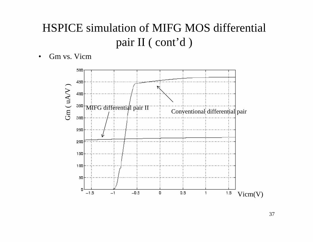
• Gm vs. Vicm
38
HSPICE simulation of MIFG MOS differential pair I
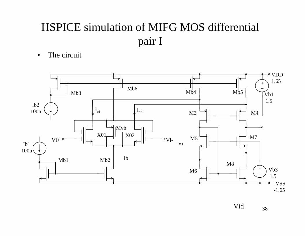
• The circuit
Vid
Vi+ Vi-
Io1 Io2
IbMb1 Mb2
X01 X02Ib1
100uVi-
M5 M7
M4M3
M6M8
Vb11.5
Vb31.5
VDD1.65
-VSS-1.65
Mb4 Mb5Mb3
Ib2100u
Mb6
Mvb
39
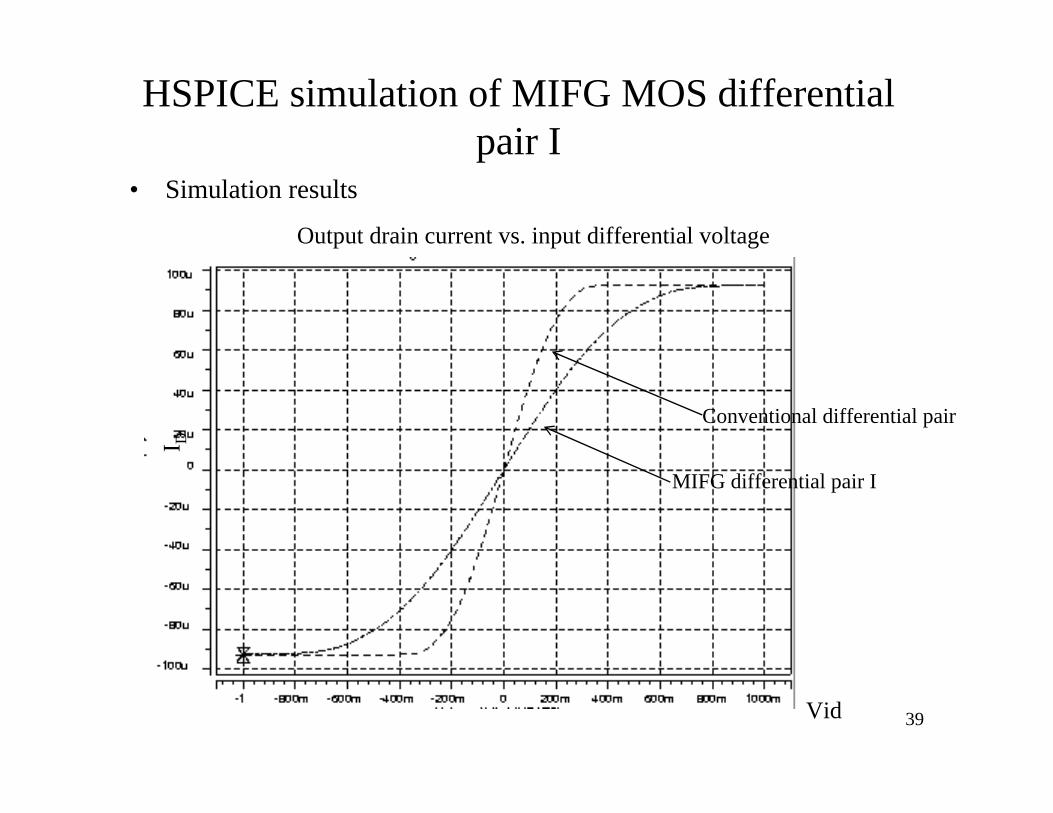
HSPICE simulation of MIFG MOS differential pair I
• Simulation results
Output drain current vs. input differential voltage
Vid
I D
Conventional differential pair
MIFG differential pair I
40
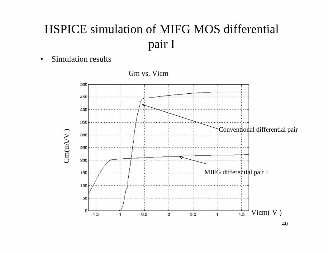
HSPICE simulation of MIFG MOS differential pair I
• Simulation results
Gm vs. Vicm
Vicm( V )
Gm
(uA
/V ) Conventional differential pair
MIFG differential pair I
41
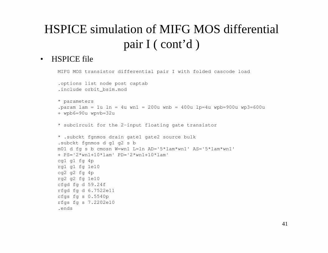
HSPICE simulation of MIFG MOS differential pair I ( cont’d )
• HSPICE fileMIFG MOS transistor differential pair I with folded cascode load
.options list node post captab
.include orbit_bsim.mod
* parameters.param lam = 1u ln = 4u wn1 = 200u wnb = 400u lp=4u wpb=900u wp3=600u+ wpb6=90u wpvb=32u
* subcircuit for the 2-input floating gate transistor
* .subckt fgnmos drain gate1 gate2 source bulk.subckt fgnmos d g1 g2 s bm01 d fg s b cmosn W=wn1 L=ln AD='5*lam*wn1' AS='5*lam*wn1'+ PS='2*wn1+10*lam' PD='2*wn1+10*lam'cg1 g1 fg 4prg1 g1 fg 1e10cg2 g2 fg 4prg2 g2 fg 1e10cfgd fg d 59.24frfgd fg d 6.7522e11cfgs fg s 0.5540p rfgs fg s 7.2202e10.ends
42
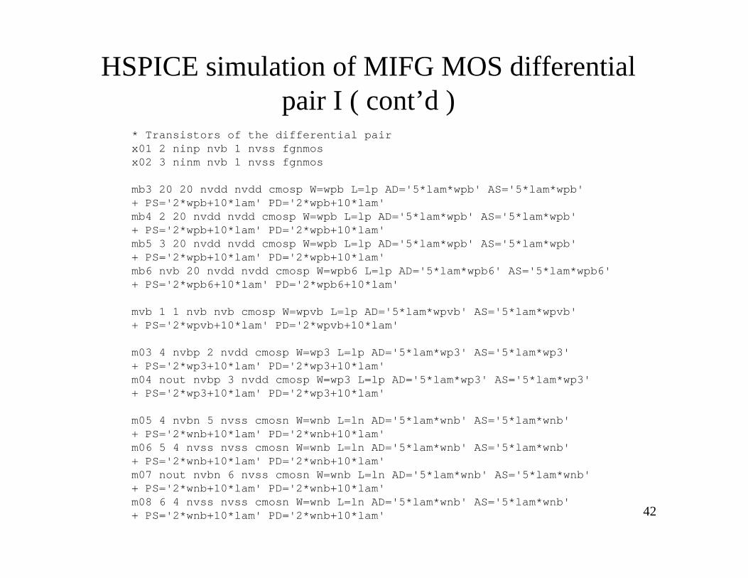
HSPICE simulation of MIFG MOS differential pair I ( cont’d )
* Transistors of the differential pairx01 2 ninp nvb 1 nvss fgnmosx02 3 ninm nvb 1 nvss fgnmos
mb3 20 20 nvdd nvdd cmosp W=wpb L=lp AD='5*lam*wpb' AS='5*lam*wpb'+ PS='2*wpb+10*lam' PD='2*wpb+10*lam'mb4 2 20 nvdd nvdd cmosp W=wpb L=lp AD='5*lam*wpb' AS='5*lam*wpb'+ PS='2*wpb+10*lam' PD='2*wpb+10*lam'mb5 3 20 nvdd nvdd cmosp W=wpb L=lp AD='5*lam*wpb' AS='5*lam*wpb'+ PS='2*wpb+10*lam' PD='2*wpb+10*lam'mb6 nvb 20 nvdd nvdd cmosp W=wpb6 L=lp AD='5*lam*wpb6' AS='5*lam*wpb6'+ PS='2*wpb6+10*lam' PD='2*wpb6+10*lam'
mvb 1 1 nvb nvb cmosp W=wpvb L=lp AD='5*lam*wpvb' AS='5*lam*wpvb'+ PS='2*wpvb+10*lam' PD='2*wpvb+10*lam'
m03 4 nvbp 2 nvdd cmosp W=wp3 L=lp AD='5*lam*wp3' AS='5*lam*wp3'+ PS='2*wp3+10*lam' PD='2*wp3+10*lam'm04 nout nvbp 3 nvdd cmosp W=wp3 L=lp AD='5*lam*wp3' AS='5*lam*wp3'+ PS='2*wp3+10*lam' PD='2*wp3+10*lam'
m05 4 nvbn 5 nvss cmosn W=wnb L=ln AD='5*lam*wnb' AS='5*lam*wnb'+ PS='2*wnb+10*lam' PD='2*wnb+10*lam'm06 5 4 nvss nvss cmosn W=wnb L=ln AD='5*lam*wnb' AS='5*lam*wnb'+ PS='2*wnb+10*lam' PD='2*wnb+10*lam'm07 nout nvbn 6 nvss cmosn W=wnb L=ln AD='5*lam*wnb' AS='5*lam*wnb'+ PS='2*wnb+10*lam' PD='2*wnb+10*lam'm08 6 4 nvss nvss cmosn W=wnb L=ln AD='5*lam*wnb' AS='5*lam*wnb'+ PS='2*wnb+10*lam' PD='2*wnb+10*lam'
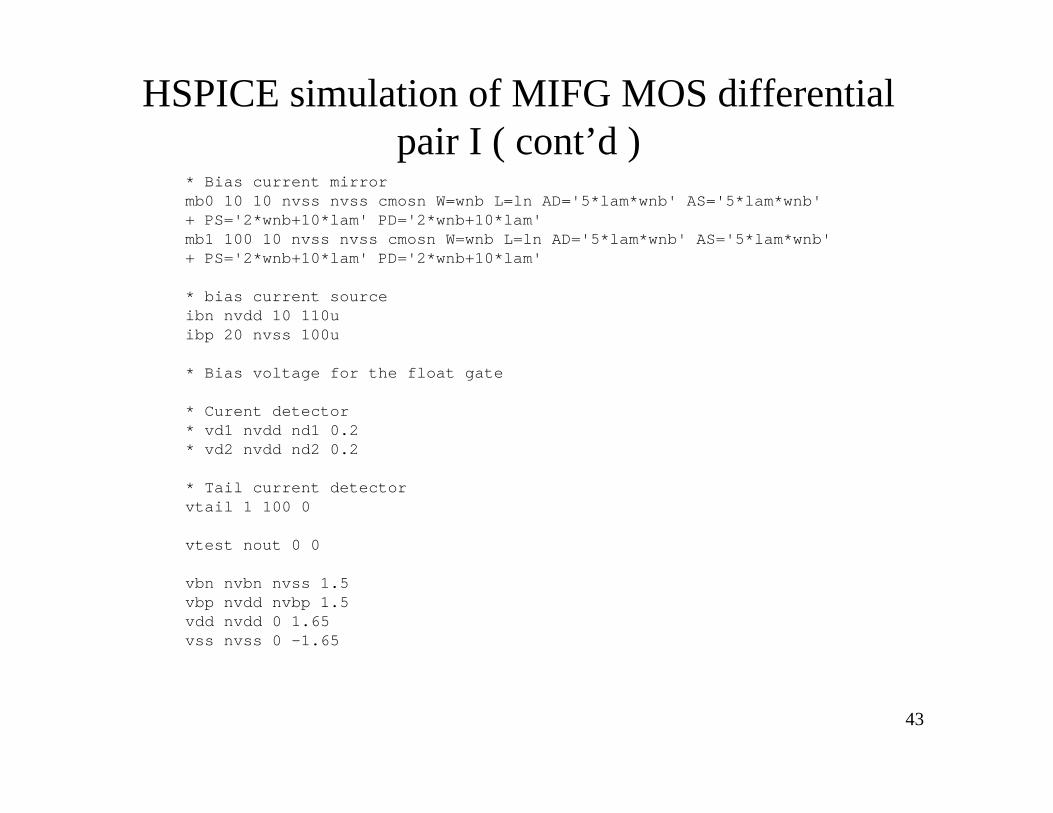
43
HSPICE simulation of MIFG MOS differential pair I ( cont’d )
* Bias current mirrormb0 10 10 nvss nvss cmosn W=wnb L=ln AD='5*lam*wnb' AS='5*lam*wnb'+ PS='2*wnb+10*lam' PD='2*wnb+10*lam'mb1 100 10 nvss nvss cmosn W=wnb L=ln AD='5*lam*wnb' AS='5*lam*wnb'+ PS='2*wnb+10*lam' PD='2*wnb+10*lam'
* bias current sourceibn nvdd 10 110uibp 20 nvss 100u
* Bias voltage for the float gate
* Curent detector* vd1 nvdd nd1 0.2* vd2 nvdd nd2 0.2
* Tail current detectorvtail 1 100 0
vtest nout 0 0
vbn nvbn nvss 1.5vbp nvdd nvbp 1.5vdd nvdd 0 1.65vss nvss 0 -1.65
44
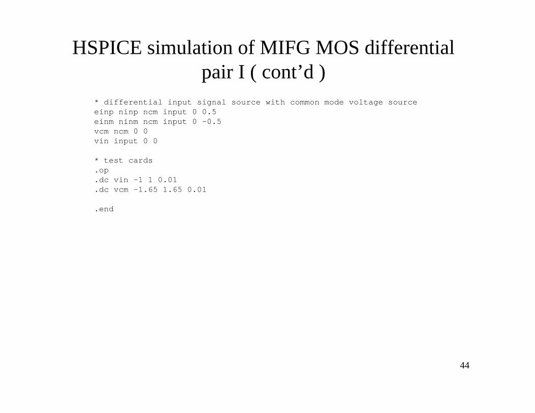
HSPICE simulation of MIFG MOS differential pair I ( cont’d )
* differential input signal source with common mode voltage sourceeinp ninp ncm input 0 0.5einm ninm ncm input 0 -0.5vcm ncm 0 0vin input 0 0
* test cards.op.dc vin -1 1 0.01.dc vcm -1.65 1.65 0.01
.end
45
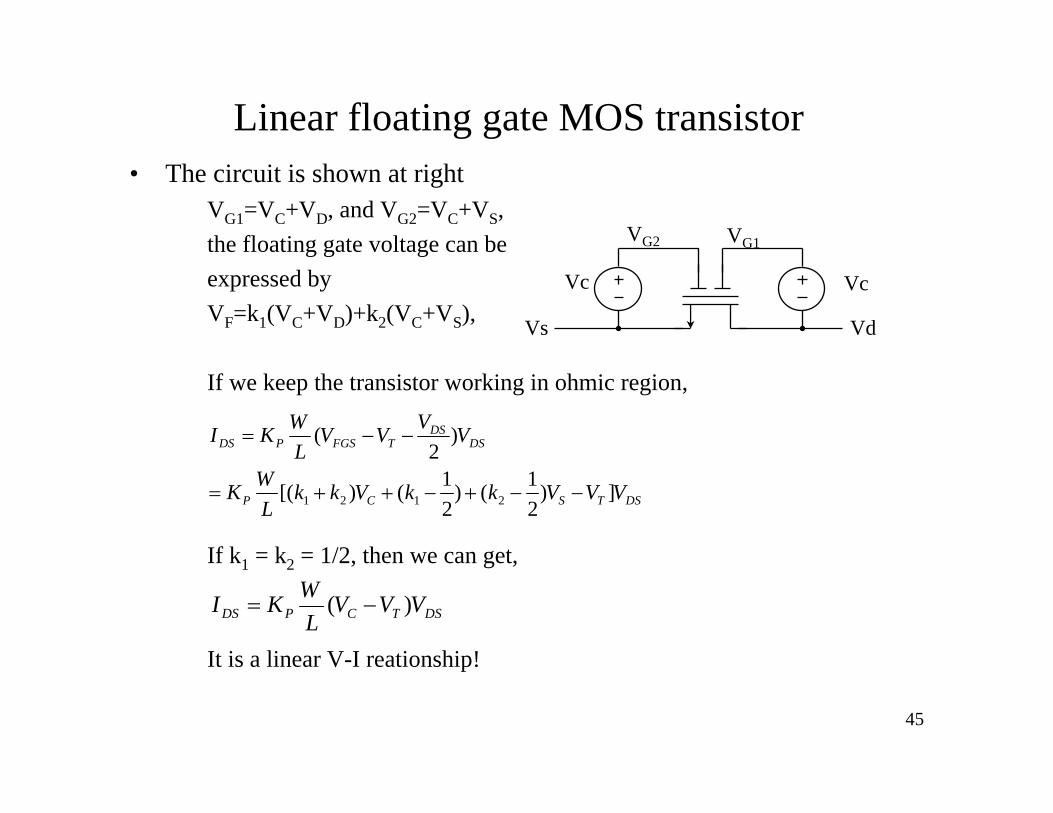
Linear floating gate MOS transistor• The circuit is shown at right
VG1=VC+VD, and VG2=VC+VS, the floating gate voltage can beexpressed byVF=k1(VC+VD)+k2(VC+VS),
If we keep the transistor working in ohmic region,
If k1 = k2 = 1/2, then we can get,
It is a linear V-I reationship!
Vc Vc
VG2 VG1
Vs Vd
DSTSCP
DSDS
TFGSPDS
VVVkkVkkL
WK
VVVVL
WKI
])21()
21()[(
)2
(
2121 −−+−++=
−−=
DSTCPDS VVVL
WKI )( −=
46
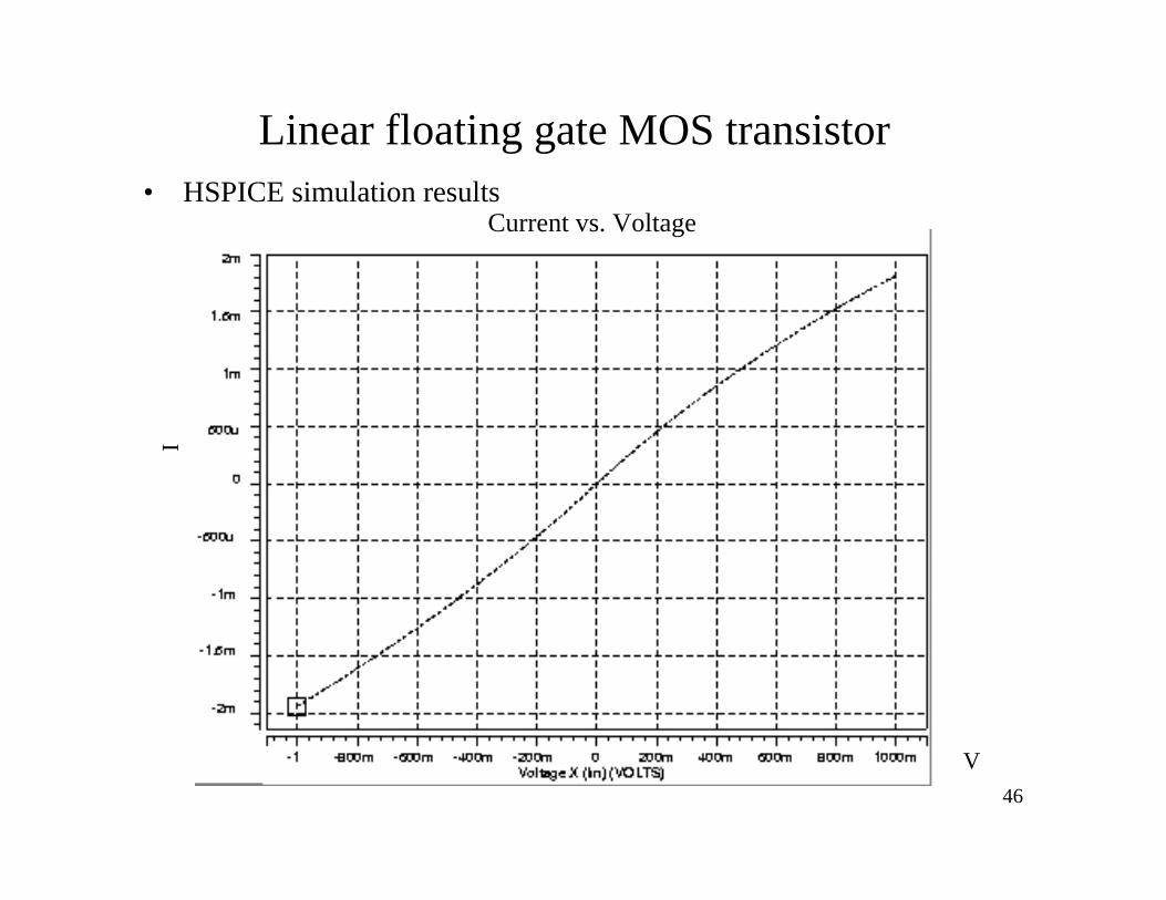
Linear floating gate MOS transistor• HSPICE simulation results
V
I
Current vs. Voltage
47
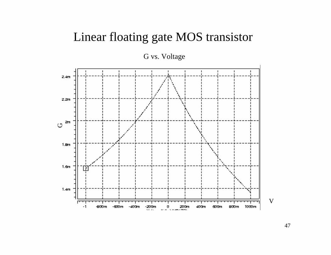
Linear floating gate MOS transistor
V
GG vs. Voltage
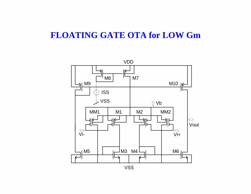
FLOATING GATE OTA for LOW Gm
Vi- Vi+
ISS
Vb
VDD
VSS
VSS
M1 M2MM1 MM2
M3 M4M5 M6
M7M8M9 M10
Vout
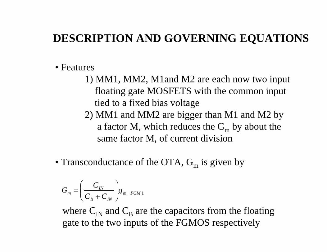
DESCRIPTION AND GOVERNING EQUATIONS
• Features1) MM1, MM2, M1and M2 are each now two input
floating gate MOSFETS with the common inputtied to a fixed bias voltage
2) MM1 and MM2 are bigger than M1 and M2 by a factor M, which reduces the Gm by about thesame factor M, of current division
• Transconductance of the OTA, Gm is given by
1_ FGMmINB
INm g
CCCG ⎟⎟
⎠
⎞⎜⎜⎝
⎛+
=
where CIN and CB are the capacitors from the floatinggate to the two inputs of the FGMOS respectively
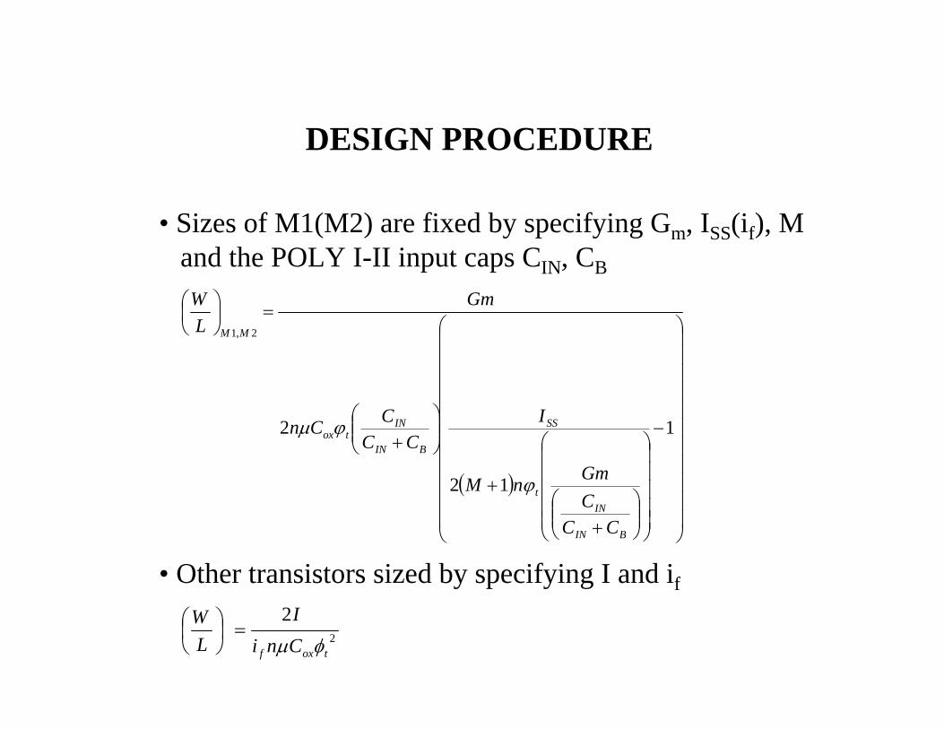
DESIGN PROCEDURE
• Sizes of M1(M2) are fixed by specifying Gm, ISS(if), Mand the POLY I-II input caps CIN, CB
• Other transistors sized by specifying I and if
2
2
toxf CniI
LW
φμ=⎟
⎠⎞
⎜⎝⎛
( )⎟⎟⎟⎟⎟⎟⎟⎟⎟⎟⎟
⎠
⎞
⎜⎜⎜⎜⎜⎜⎜⎜⎜⎜⎜
⎝
⎛
−
⎟⎟⎟⎟⎟
⎠
⎞
⎜⎜⎜⎜⎜
⎝
⎛
⎟⎟⎠
⎞⎜⎜⎝
⎛+
+
⎟⎟⎠
⎞⎜⎜⎝
⎛+
=⎟⎠⎞
⎜⎝⎛
1
12
2
2,1
BIN
INt
SS
BIN
INtox
MM
CCCGmnM
ICC
CCn
GmL
W
ϕ
ϕμ
51
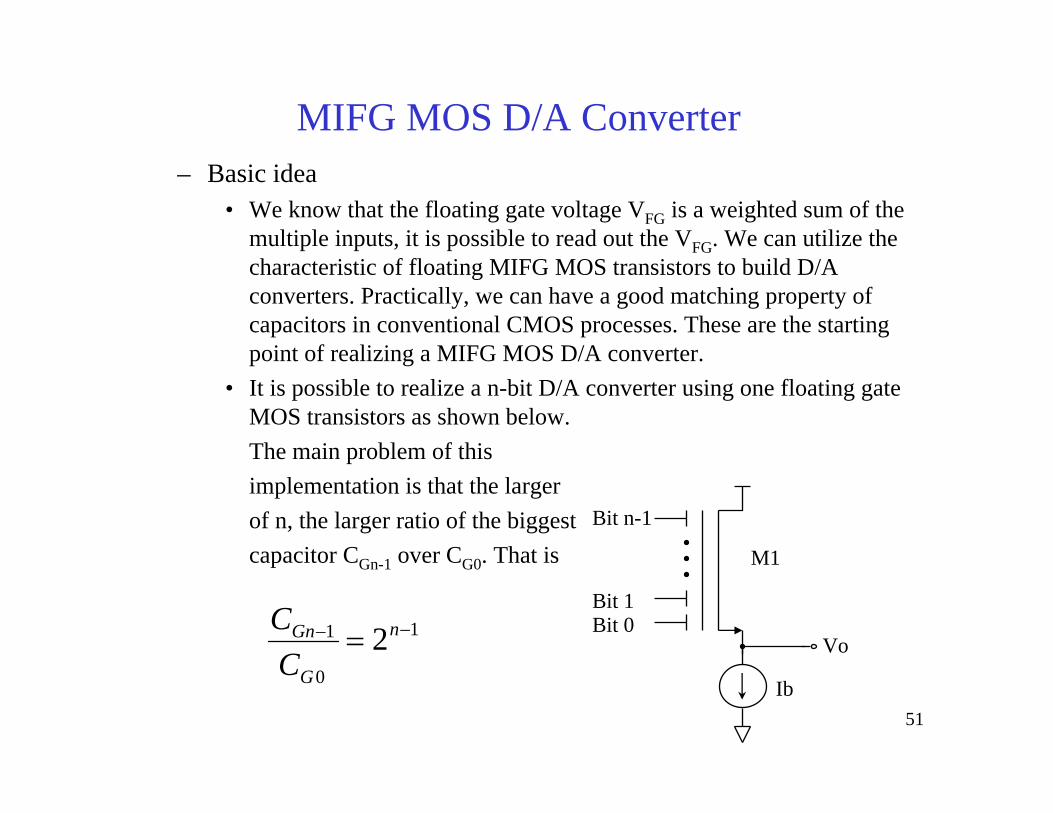
MIFG MOS D/A Converter– Basic idea
• We know that the floating gate voltage VFG is a weighted sum of the multiple inputs, it is possible to read out the VFG. We can utilize the characteristic of floating MIFG MOS transistors to build D/A converters. Practically, we can have a good matching property ofcapacitors in conventional CMOS processes. These are the starting point of realizing a MIFG MOS D/A converter.
• It is possible to realize a n-bit D/A converter using one floating gate MOS transistors as shown below.The main problem of thisimplementation is that the largerof n, the larger ratio of the biggestcapacitor CGn-1 over CG0. That is
Bit 0Bit 1
Bit n-1
Ib
M1
Vo1
0
1 2 −− = n
G
Gn
CC
52
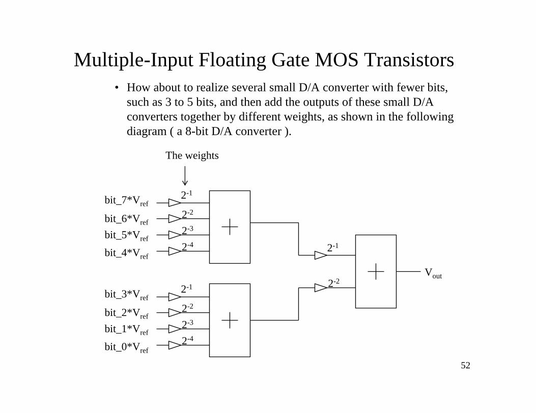
Multiple-Input Floating Gate MOS Transistors• How about to realize several small D/A converter with fewer bits,
such as 3 to 5 bits, and then add the outputs of these small D/Aconverters together by different weights, as shown in the following diagram ( a 8-bit D/A converter ).
2-1
2-2
2-3
2-4
The weights
bit_4*Vref
bit_5*Vref
bit_6*Vref
bit_7*Vref
2-1
2-2
2-3
2-4bit_0*Vref
bit_1*Vref
bit_2*Vref
bit_3*Vref
2-1
2-2Vout
53
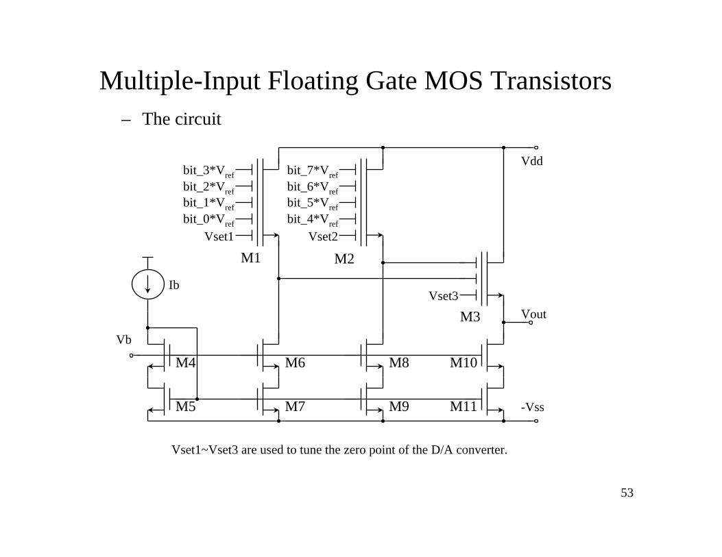
Multiple-Input Floating Gate MOS Transistors– The circuit
bit_0*Vref
bit_1*Vref
bit_2*Vref
bit_3*Vref
Vset1bit_4*Vref
bit_5*Vref
bit_6*Vref
bit_7*Vref
Vset2
Vset3Vout
Vdd
-Vss
Vb
Ib
M1 M2
M3
M4
M5
M6
M7
M8
M9
M10
M11
Vset1~Vset3 are used to tune the zero point of the D/A converter.
54
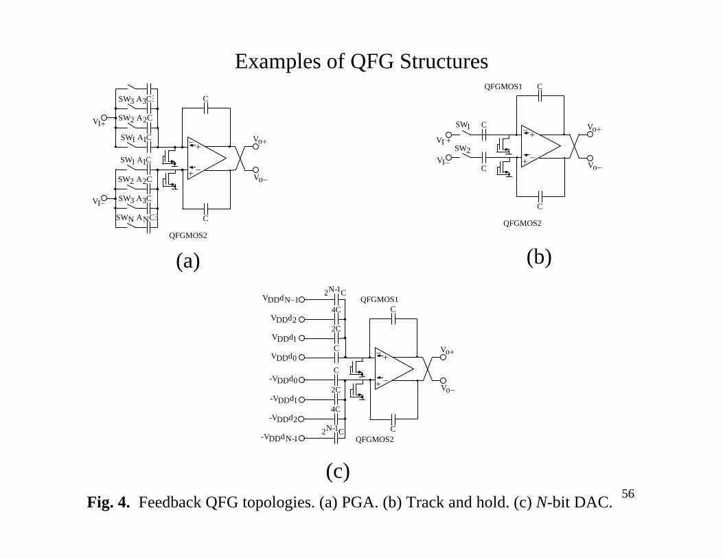
NV
2V
1V1C
2C
NC
BIAS1N VV =+
LARGEC
GDC
GSCGBC
SV
BVGV
NV
2V
1V1C
2C
NC
GDC
GSCGBC
SV
BVGV
leakRGD'C
(b) (d)
M
DV
DVSSV
(a) (c)
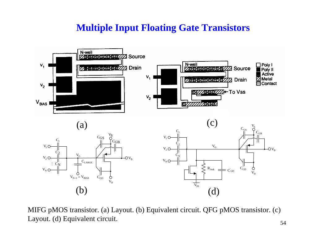
MIFG pMOS transistor. (a) Layout. (b) Equivalent circuit. QFG pMOS transistor. (c) Layout. (d) Equivalent circuit.
Multiple Input Floating Gate Transistors
55
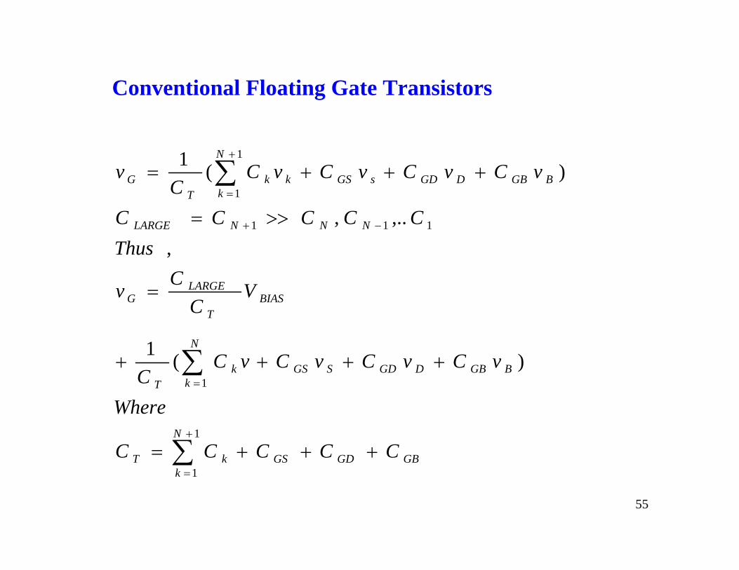
Conventional Floating Gate Transistors
GBGDGS
N
kkT
N
kBGBDGDSGSk
T
BIAST
LARGEG
NNNLARGE
BGBDGDsGSk
N
kk
TG
CCCCC
Where
vCvCvCvCC
VC
Cv
ThusCCCCC
vCvCvCvCC
v
+++=
++++
=
>>=
+++=
∑
∑
∑
+
=
=
−+
+
=
1
1
1
111
1
1
)(1
,,..,
)(1
56
+
−
C
C
+oV
−oV
QFGMOS2
+
−
−IV
+IV
C
C
1SW
2SW
QFGMOS1
(b)
+
−
MC3A 3SW
C2A 2SW
C1A 1SW
C2A 2SW
C3A 3SW
MCNA NSW
C1A 1SW
C
C
+oV
−oV
+IV
−IV
QFGMOS2
(a)
+
−
+
−
C1-N2
2C
C
2C
4C
C1-N2
C
C
C
+oV
−oV
1NdDDV −
QFGMOS2
+
−
4C2dDDV
1dDDV
0dDDV
0dDD-V
1dDD-V
2dDD-V
1-NdDD-V
QFGMOS1
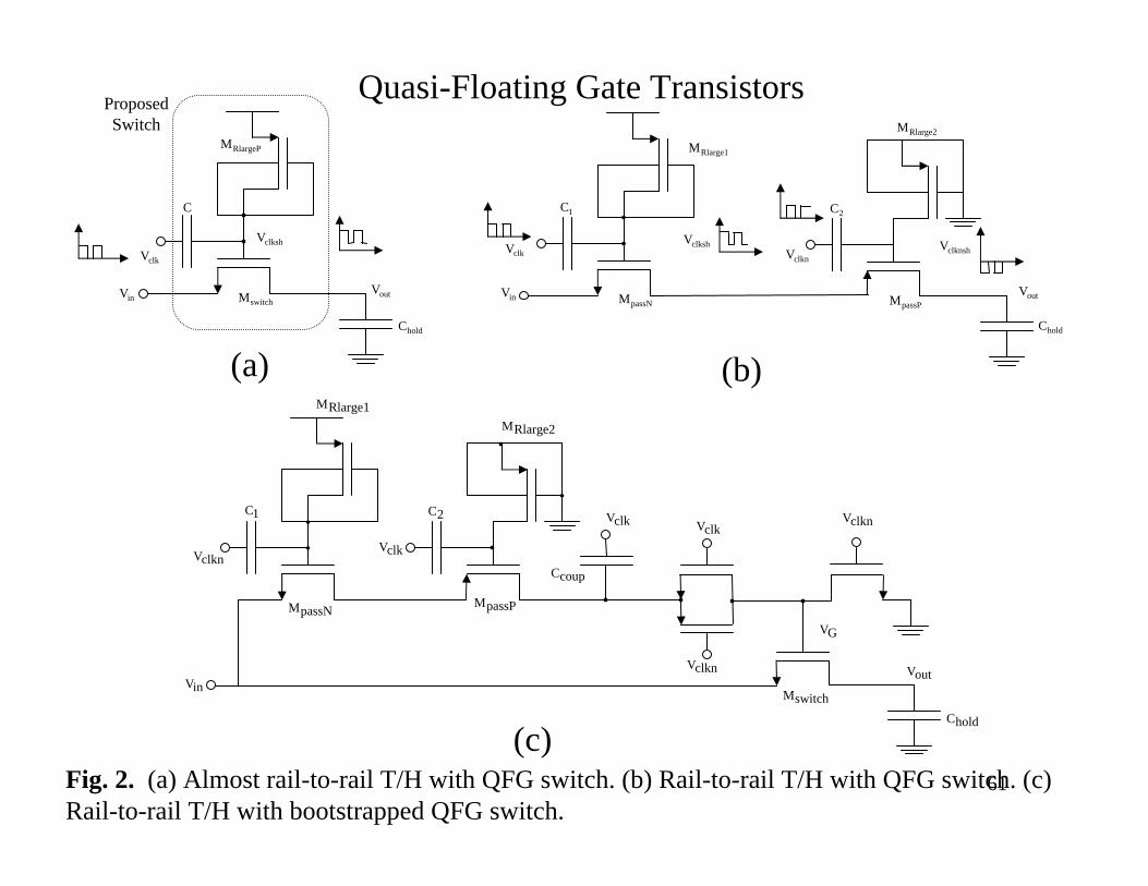
(c)Fig. 4. Feedback QFG topologies. (a) PGA. (b) Track and hold. (c) N-bit DAC.
Examples of QFG Structures
57
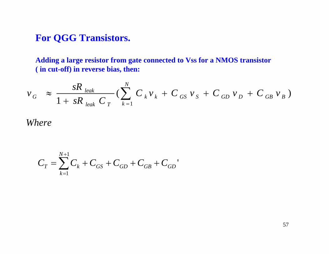
Where
vCvCvCvCCsR
sRv BGBDGDSGSk
N
kk
Tleak
leakG )(
1 1+++
+≈ ∑
=
For QGG Transistors.
Adding a large resistor from gate connected to Vss for a NMOS transistor( in cut-off) in reverse bias, then:
'1
1GDGBGDGS
N
kkT CCCCCC ++++=∑
+
=
58
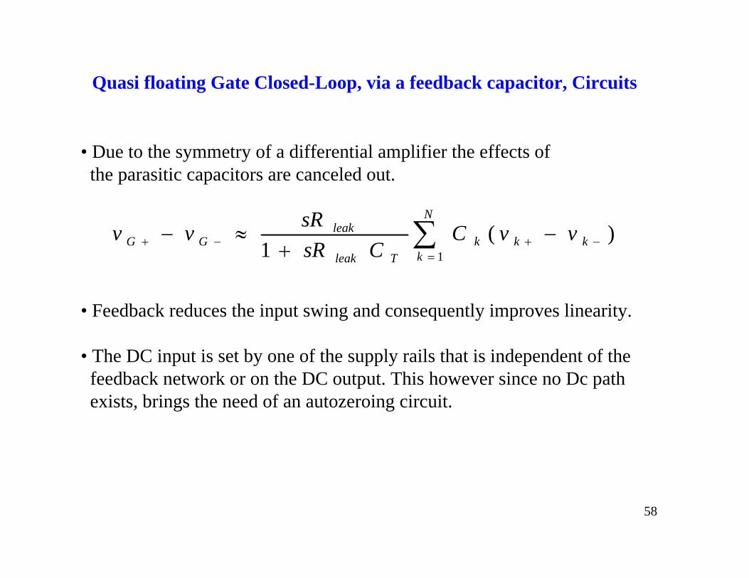
Quasi floating Gate Closed-Loop, via a feedback capacitor, Circuits
• Due to the symmetry of a differential amplifier the effects of the parasitic capacitors are canceled out.
• Feedback reduces the input swing and consequently improves linearity.
• The DC input is set by one of the supply rails that is independent of the feedback network or on the DC output. This however since no Dc path exists, brings the need of an autozeroing circuit.
)(1 1
−+=
−+ −+
≈− ∑ kk
N
kk
Tleak
leakGG vvC
CsRsRvv
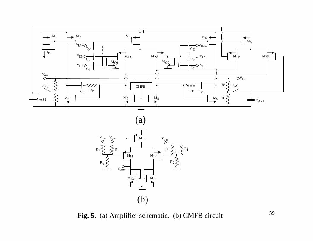
59Fig. 5. (a) Amplifier schematic. (b) CMFB circuit
1AM 2AM
CMFBcR cC
9M
1R
1R
1SW
AZ1C8M7M6McC cR
AZ2C
2SW
+oV+oV
+I1V
+I2V
+INVNC
2C
1C
Q1M
1M 2M 3M 4M5M
1BM 2BMBI
Q2M
−INV
−2IV
−1IV
NC
2C
1C
10M
1R
cmV
1R
2R
1R 1R
2R
13M
cmoV
14M
11M 12M
+oV −oV
(a)
(b)
60
Fig. 7
Fig. 7
Fig. 8
Fig. 9
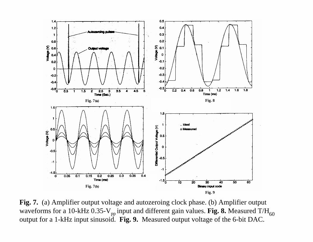
Fig. 7. (a) Amplifier output voltage and autozeroing clock phase. (b) Amplifier output waveforms for a 10-kHz 0.35-Vpp input and different gain values. Fig. 8. Measured T/H output for a 1-kHz input sinusoid. Fig. 9. Measured output voltage of the 6-bit DAC.
61
2C
outV
holdC
clkshVclknshV
1C
Rlarge1M
passNM passPM
Rlarge2M
clknVclkV
(b)
inV
inVoutV
switchM
passPMpassNM
clknV
1C 2C
Rlarge1M
Rlarge2M
clkVclkV clknV
GV
clknV
holdC
clkV
coupC
(c)
RlargePM
clkVclkshV
inVswitchM outV
holdC
(a)
C
Proposed Switch
Fig. 2. (a) Almost rail-to-rail T/H with QFG switch. (b) Rail-to-rail T/H with QFG switch. (c) Rail-to-rail T/H with bootstrapped QFG switch.
Quasi-Floating Gate Transistors
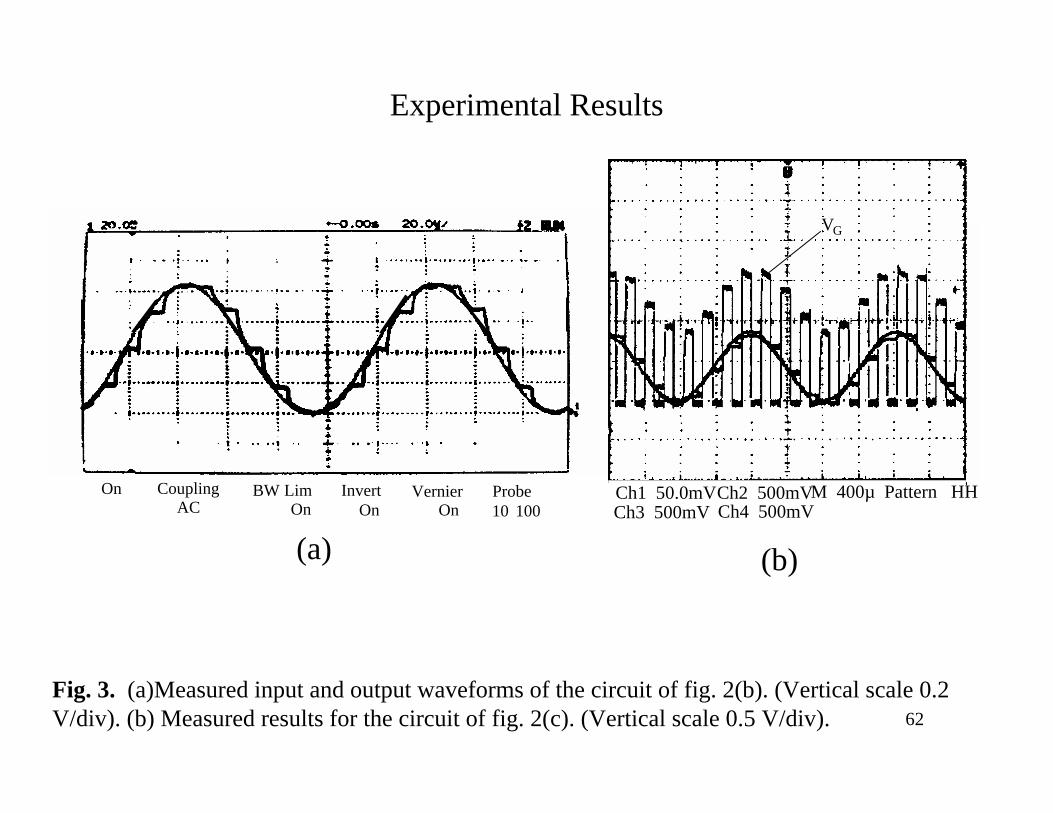
62Fig. 3. (a)Measured input and output waveforms of the circuit of fig. 2(b). (Vertical scale 0.2 V/div). (b) Measured results for the circuit of fig. 2(c). (Vertical scale 0.5 V/div).
On Coupling LimBW AC
InvertOn
VernierOn
ProbeOn 10010
(a)
Ch1 50.0mVCh2 500mVM 400µ Pattern HHCh3 500mV Ch4 500mV
(b)
GV
Experimental Results
63
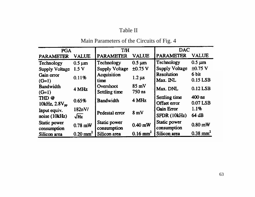
Table II
Main Parameters of the Circuits of Fig. 4
64
References• “Solution to the Trapped Charge in FGMOS Transistor”, E. Rodriguez-Villegas and H.
Barnes, IEE Electronic Letters 39 (19) pp.1416-1417, Sep. 2003 • “A Low-Voltage Low-Power QFG-based Sigma-Delta Modulator for
Electroencephalogram Applications”, E. López-Morillo, Ramon Gonzalez-Carvajal, J. Galan, J. Ramirez-Angulo, A. Lopez Martin and E.Rodriguez-Villegas, IEEE BioCAS, pp. 118-121, Dec. 2006.
• “ A new family of low-voltage circuits based on quasi-floating gate transistors” Urquidi, C. Ramirez-Angulo, J. Gonzalez-Carvajal, R. Torralba, A. Midwest Symposium on Circuits and Systems, 2002. MWSCAS-2002.
• Overview of floating-gate devices, circuits, and systemsP Hasler, TS Lande - IEEE Transactions on Circuits and Systems II: Analog and …, 2001 -ieeexplore.ieee.org