fabrication and optical characteristics of silicon-based two-dimensional photonic crystal...
TRANSCRIPT

ARTICLE IN PRESS
1386-9477/$ - se
doi:10.1016/j.ph
�Tel.: +886 3
E-mail addr
Physica E 40 (2008) 2800–2804
www.elsevier.com/locate/physe
Fabrication and optical characteristics of silicon-based two-dimensionalphotonic crystal Mach–Zehnder interferometers
Chen-Yang Liu�
Center for Measurement Standards, Industrial Technology Research Institute, Room B03, Building 16, 321, Sec. 2, Kuang Fu Road, Hsinchu, Taiwan
Received 3 October 2007; received in revised form 17 December 2007; accepted 19 December 2007
Available online 5 January 2008
Abstract
Photonic crystals have many potential applications because of their ability to control light-wave propagation. We report on the
fabrication and properties of quasi-two-dimensional photonic crystals with triangular lattices of dielectric rods in air. Rod-type photonic
crystal structures were fabricated in silicon by electron beam lithography and dry-etching techniques. Mach–Zehnder interferometers
were fabricated from two-dimensional photonic crystal waveguides. Transmission spectra were measured and device operation was
shown to be in agreement with theoretical calculations. The interferometers can be used in the visible light region. Such an approach to
photonic element systems should enable new applications for designing components in photonic integrated circuits.
r 2008 Elsevier B.V. All rights reserved.
PACS: 42.70.Qs; 42.79.�e
Keywords: Photonic crystal; Mach–Zehnder interferometer; Electron beam lithography
1. Introduction
Recently, there has been growing interests in studies ofthe propagation of electromagnetic waves in periodicdielectric structures [1]. These structures exhibit forbiddenfrequency regions where electromagnetic waves cannotpropagate for both polarizations along any direction. Thismay bring about some peculiar physical phenomena. Theconcept of photonic crystal (PC) waveguides and relateddevice applications in integrated optics have been discussed[2], as well as some of the fabrication technology required torealize these structures [3]. It has been shown that dopedPCs permit the guiding of waves in two different geometricpaths for two distinct wavelength ranges [4]. Such structurescan be used to design highly efficient new optical devices.Optical waveguides in two-dimensional (2-D) PCs producedby insertion of linear defects into PC structures had beenproposed [5] and experimentally demonstrated [6]. PlanarPC circuits consist of devices such as splitters [7], filters [8],and multichannel drop filters [9], by controlling the
e front matter r 2008 Elsevier B.V. All rights reserved.
yse.2007.12.007
5743765; fax: +886 3 5726445.
ess: [email protected]
interaction between static devices, such as waveguides,cavities, or horns. A simple theoretical model of aMach–Zehnder interferometer consisting of two coupled-resonator optical waveguides with different lengths wasproposed and has been experimentally demonstrated atmicrowave frequencies [10]. Compared to different devices,the relative length of the arms of the Mach–Zehnderinterferometer was changed. The realization of a thermo-optically controlled symmetric Mach–Zehnder interferom-eter switch, based on an AlGaAs/GaAs epitaxial waveguidestructure operating at wavelengths in the region of l ¼1550 nm, has been reported [11] and a tunable PCwaveguide Mach–Zehnder interferometer, achieved bynematic liquid crystal phase modulation, has been docu-mented by the authors [12]. Consequently, Mach–Zehnderinterferometers in planar PCs may become key buildingblocks in the development of photonic integrated circuitssuch as switches and modulators.In these respects, three-dimensional (3-D) PC structures
are the most promising. However, since they are difficult tofabricate using existing techniques, 2-D PC structures haveemerged as alternative systems. 2-D PC structures withtriangular lattice have become widely popular due to their

ARTICLE IN PRESS
Fig. 1. Schematic diagram of Mach–Zehnder interferometers in 2-D rod-
type PCs with path-length differences of (a) 0 and (b) 9a. Inset, lattice
constant a and radius of rods r.
C.-Y. Liu / Physica E 40 (2008) 2800–2804 2801
spectrally broad and complete photonic bandgap. Thefabrication and properties of 2-D PCs with honeycomblattices of dielectric rods in air have been discussed [13].Square lattice rod-type PC slabs were successfully demon-strated recently by two independent groups of researchers[14,15]. They have experimentally demonstrated the guid-ing of light at a 1.5 mm wavelength in straight and 901-bentline-defect waveguides in 2-D square-lattice-of-rods PCslabs. The design, fabrication and measurement of PCwaveguide devices working at the optical communicationwavelengths had been a critical issue.
We have fabricated Mach–Zehnder interferometers in2-D PCs, with path-length differences between the armsof the interferometer, and rod-type PCs in silicon byelectron beam lithography and dry-etching techniques.The Mach–Zehnder interferometers were composed of2-D PC waveguides. Transmission spectra were measuredand device operation was shown to be in agreementwith theoretical calculations. These results suggest a newapplication for designing components in photonic inte-grated circuits. The remainder of this paper is devoted tothe associated calculation and fabrication details, as well asa discussion of the results.
2. Rod-type 2-D PC Mach–Zehnder interferometer design
We consider a PC waveguide Mach–Zehnder interfe-rometer composed of dielectric rods in air in a triangulararray with lattice constant a=0.38 mm. The radius and therefractive index of the rods are taken as r=0.26a andn=3.4 (Si), respectively. A well-known plane wave expan-sion calculation yields the photonic band structure for thetriangular array of dielectric columns [16]. Therefore thisPC structure has a photonic bandgap for transversemagnetic modes that extends from l ¼ 0.48 to 0.54 mm,where l is the wavelength in free space. We have designedMach–Zehnder interferometers in 2-D PCs with a range ofpath-length differences between the two arms of theinterferometers. This amplitude-splitting interferometeruses two Y junctions and two arms. The incident light isdivided into two arms. The relative phase of the two armsis determined by the intensity of the light. We expecttherefore that the intensity transmitted through theinterferometers will exhibit oscillations as a function ofthe optical frequency with a period that depends on thepath-length difference and the propagation coefficient.If the path-length difference is an even multiple ofwavelengths, the output will be a maximum and if thepath-length difference is an odd multiple of half-wave-lengths, the output will be a minimum. Mach–Zehnderinterferometers with path-length differences between thetwo arms of 0 and of 9a were designed and are shown inFig. 1.
The finite-difference time-domain (FDTD) method is apowerful, accurate numerical method that permits compu-ter-aided design and simulation of PC devices. It usescentral-difference approximations for numerical derivatives
in space and time, both with second-order accuracy. TheFDTD calculation is applied to the 2-D case. The photonicdevice is laid out in the x–z plane. The propagation is alongthe z direction. The space steps in the x and z directions areDx and Dz, respectively. The sampling in space is on asubwavelength scale. Typically, 10–20 steps per wavelengthare needed. We assume that Dx ¼ 0.05 and Dz ¼ 0.05.Sampling in time is selected to ensure numerical stability ofthe algorithm. The time step is determined by the Courantlimit [17]. A more-detailed treatment of the FDTD methodis given in Ref. [17]. We investigated interference propertiesof PC interferometers numerically by using a 2-D FDTDsimulation. Fig. 2 shows the electric field patterns observedin the frequency domain of the PC waveguide Mach–Zehnder interferometer with path-length differences of 0and 9a. TM-polarized continuous wave light with Gaussianprofile and l ¼ 0.532 mm is input into port 1. We cansee that the output reaches a maximum, as shown inFig. 2(a), when the recombined light is in phase and thatthe interferometer output is null, as shown in Fig. 2(b),
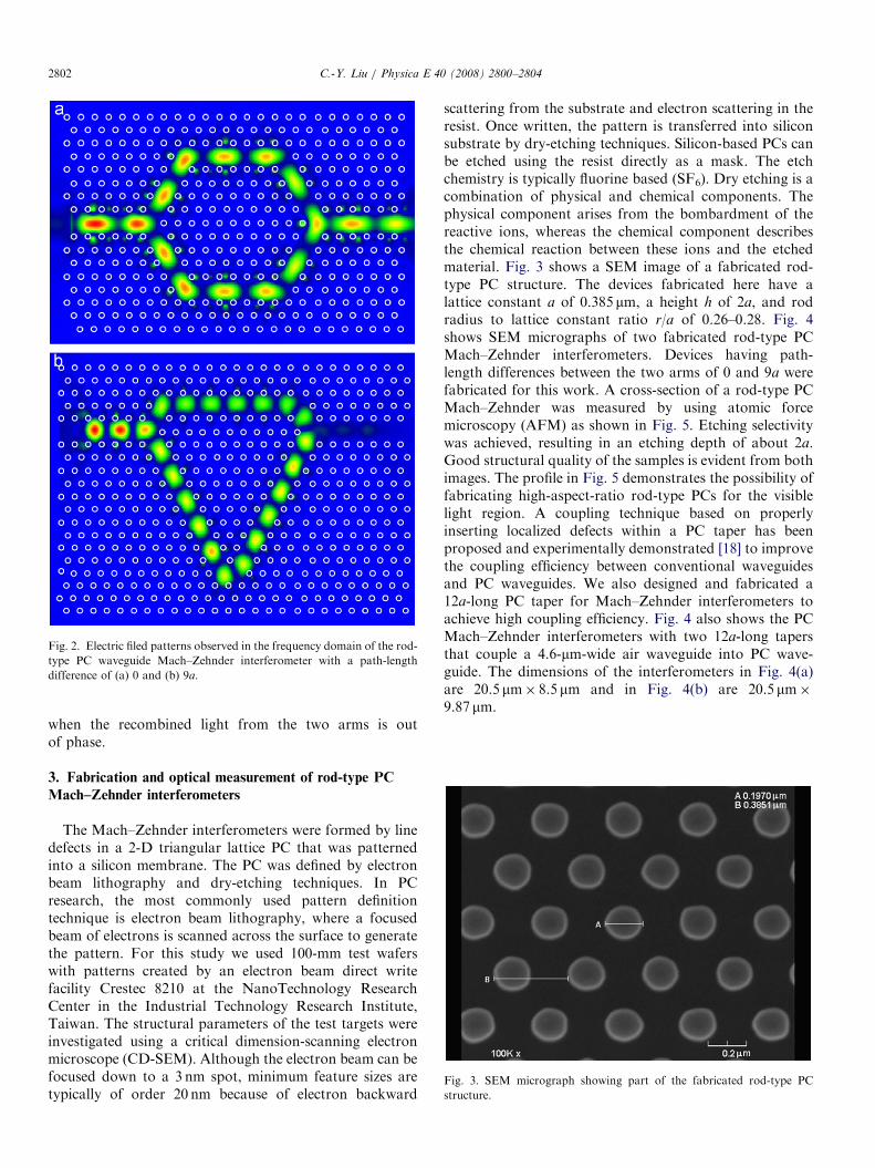
ARTICLE IN PRESS
Fig. 2. Electric filed patterns observed in the frequency domain of the rod-
type PC waveguide Mach–Zehnder interferometer with a path-length
difference of (a) 0 and (b) 9a.
Fig. 3. SEM micrograph showing part of the fabricated rod-type PC
structure.
C.-Y. Liu / Physica E 40 (2008) 2800–28042802
when the recombined light from the two arms is outof phase.
3. Fabrication and optical measurement of rod-type PC
Mach–Zehnder interferometers
The Mach–Zehnder interferometers were formed by linedefects in a 2-D triangular lattice PC that was patternedinto a silicon membrane. The PC was defined by electronbeam lithography and dry-etching techniques. In PCresearch, the most commonly used pattern definitiontechnique is electron beam lithography, where a focusedbeam of electrons is scanned across the surface to generatethe pattern. For this study we used 100-mm test waferswith patterns created by an electron beam direct writefacility Crestec 8210 at the NanoTechnology ResearchCenter in the Industrial Technology Research Institute,Taiwan. The structural parameters of the test targets wereinvestigated using a critical dimension-scanning electronmicroscope (CD-SEM). Although the electron beam can befocused down to a 3 nm spot, minimum feature sizes aretypically of order 20 nm because of electron backward
scattering from the substrate and electron scattering in theresist. Once written, the pattern is transferred into siliconsubstrate by dry-etching techniques. Silicon-based PCs canbe etched using the resist directly as a mask. The etchchemistry is typically fluorine based (SF6). Dry etching is acombination of physical and chemical components. Thephysical component arises from the bombardment of thereactive ions, whereas the chemical component describesthe chemical reaction between these ions and the etchedmaterial. Fig. 3 shows a SEM image of a fabricated rod-type PC structure. The devices fabricated here have alattice constant a of 0.385 mm, a height h of 2a, and rodradius to lattice constant ratio r/a of 0.26–0.28. Fig. 4shows SEM micrographs of two fabricated rod-type PCMach–Zehnder interferometers. Devices having path-length differences between the two arms of 0 and 9a werefabricated for this work. A cross-section of a rod-type PCMach–Zehnder was measured by using atomic forcemicroscopy (AFM) as shown in Fig. 5. Etching selectivitywas achieved, resulting in an etching depth of about 2a.Good structural quality of the samples is evident from bothimages. The profile in Fig. 5 demonstrates the possibility offabricating high-aspect-ratio rod-type PCs for the visiblelight region. A coupling technique based on properlyinserting localized defects within a PC taper has beenproposed and experimentally demonstrated [18] to improvethe coupling efficiency between conventional waveguidesand PC waveguides. We also designed and fabricated a12a-long PC taper for Mach–Zehnder interferometers toachieve high coupling efficiency. Fig. 4 also shows the PCMach–Zehnder interferometers with two 12a-long tapersthat couple a 4.6-mm-wide air waveguide into PC wave-guide. The dimensions of the interferometers in Fig. 4(a)are 20.5 mm� 8.5 mm and in Fig. 4(b) are 20.5 mm�9.87 mm.

ARTICLE IN PRESS
Fig. 4. SEM images of the PC Mach–Zehnder interferometer with a path-
length difference of (a) 0 and (b) 9a and two 12a-long tapers that couple a
4.6 mm-wide air waveguide into PC waveguide. The dimensions of the
entire interferometer: (a) 20.5mm� 8.5 mm and (b) 20.5mm� 9.87mm.
Fig. 5. Cross-section of rod-type PC Mach–Zehnder measured by using
atomic force microscopy.
C.-Y. Liu / Physica E 40 (2008) 2800–2804 2803
A lensed fiber was used to launch TM-polarized lightfrom a tunable broadband laser into the PC Mach–Zehnderinterferometers, and a cleaved single-mode fiber was usedto collect the output signal. The sample was mounted on atranslation stage capable of 10-nm resolution, and TM-polarized light was coupled into the waveguide with a highnumerical aperture fiber lens assembly. The light outputfrom the waveguide was detected with another optical fiberat the opposite end, and directly introduced to an opticalpower meter. The measured characteristics and thecomputer-simulated transmission characteristics, obtainedusing the 2-D FDTD approach, are shown in Fig. 6. Themeasurement and simulation show close agreement. Wecan see that the output reaches a maximum, as shown inFig. 6(a), when the recombined light is in phase andthat the interferometer output is nearly null, as shown inFig. 6(b), when the recombined light from the two arms isout of phase. The light propagation of rod-type PCinterferometer depends on the photonic bandgap, working
wavelengths, and path-length differences between the twoarms of interferometer.The waveguide propagation losses include out-of-plane
leakage [19] and roughness scattering [20] in the PCwaveguides. Out-of-plane leakage provides the majorsource of propagation loss. Additionally, there is rough-ness scattering arising from fabrication imperfections. Inhole-type PC structures, the medium of line defectwaveguide is silicon. It is known that silicon is absorbingin the visible light region when light propagates in silicon.Therefore most devices of the hole-type PC structure workat the optical communication wavelengths. However, themedium of the single line defect waveguide is air in the rod-type PC Mach–Zehnder interferometers. According to thesimulations and measurements, the transmission loss isclose to 1%. The absorption in the silica rods should alsobe very small because the size of silica rods is about 200 nm.The interferometers can be used in the visible light region.This is one of the merits of the rod-type PC. Rod-type PCdevices can be certainly used in the infrared light region.Further, the size of rod-type PC interferometer working inthe visible light region is smaller than that of the hole-typePC interferometer working at optical communicationwavelengths since the dimensions of lattice constant androd depend on the photonic bandgap and workingwavelengths. In this paper, we assume that the absorptionloss is negligible. More complex simulations and measure-ments are necessary. We are currently examining 3-D PCsimulations and measurements—including out-of-planeleakage and roughness scattering, with the goal ofcomparing these new experimental and theoretical data.

ARTICLE IN PRESS
Fig. 6. Transmission spectra of the PC Mach–Zehnder interferometer
with a path-length difference of (a) 0 and (b) 9a.
C.-Y. Liu / Physica E 40 (2008) 2800–28042804
4. Conclusion
In this paper, we have numerically and experimentallydemonstrated certain properties of Mach–Zehnder inter-ferometers in 2-D PCs with path-length differences betweenthe arms of the interferometer. The associated rod-typePCs were fabricated in silicon using electron beam
lithography and dry-etching techniques. Transmissionspectra were measured and the device operation was shownto be in agreement with theoretical calculations. Such anapproach to photonic element systems should provide newapplications for designing components in photonic inte-grated circuits. However, additional theoretical investiga-tions and experimental efforts are needed in order to bringthe rod-type PC devices to mature fruition.
References
[1] E. Yablonovitch, Phys. Rev. Lett. 58 (1987) 2059.
[2] J.D. Joannopoulos, R.D. Meade, J.N. Winn, Photonic Crystals:
Molding the Flow of Light, Princeton University Press, New Jersey,
1995.
[3] T.F. Krauss, Phys. Stat. Sol. (a) 197 (2003) 688.
[4] E. Centeno, D. Felbacq, Opt. Commun. 160 (1999) 57.
[5] R.D. Meade, A. Devenyi, J.D. Joannopoulos, O.L. Alerhand,
D.A. Smith, K. Kash, J. Appl. Phys. 75 (1994) 4753.
[6] T. Baba, N. Fukaya, J. Yonekura, Electron. Lett. 35 (1999) 654.
[7] S. Fan, S.G. Johnson, J.D. Joannopoulos, C. Manolatou, H.A. Haus,
J. Opt. Soc. Am. B 18 (2001) 162.
[8] R. Costa, A. Melloni, M. Martinelli, Photon. Technol. Lett. 15 (2003)
401.
[9] A. Sharkawy, S. Shi, D.W. Prather, Appl. Opt. 40 (2001) 2247.
[10] A. Martinez, A. Griol, P. Sanchis, J. Marti, Opt. Lett. 28 (2003) 405.
[11] E.A. Camargo, H.M.H. Chong, R.M. De La Rue, Opt. Express 12
(2004) 588.
[12] C.-Y. Liu, L.-W. Chen, Opt. Express 12 (2004) 2616.
[13] J.-Y. Ye, V. Mizeikis, Y. Xu, S. Matsuo, H. Misawa, Opt. Commun.
211 (2002) 205.
[14] M. Tokushima, H. Yamada, Y. Arakawa, Appl. Phys. Lett. 84 (2004)
4298.
[15] S. Assefa, P.T. Bienstman, S.G. Johnson, G.S. Petrich,
J.D. Joannopoulos, L.A. Kolodziejski, E.P. Ippen, H.I. Smith, Appl.
Phys. Lett. 85 (2004) 6110.
[16] C.-Y. Liu, L.-W. Chen, Phys. Rev. B 72 (2005) 045133.
[17] A. Taflove, S.C. Hagness, Computational Electrodynamics: The
Finite Difference Time Domain Method, Artech House, Boston,
1998.
[18] A. Hakansson, P. Sanchis, J. Sanchez-Dehesa, J. Martı, J. Lightw.
Technol. 23 (2005) 3881.
[19] G.R. Hadley, Photon. Technol. Lett. 14 (2002) 642.
[20] H. Benisty, C. Weisbuch, D. Labilloy, M. Rattier, C.J.M. Smith,
T.F. Krauss, R.M. De La Rue, R. Houdre, U. Oesterle, C. Jouanin,
D. Cassagne, J. Lightw. Technol. 17 (1999) 2063.