epitaxial tbmno3 thin films on srtio3 substrates: a ... · iop publishing journal of physics:...
TRANSCRIPT

University of Groningen
Epitaxial TbMnO3 thin films on SrTiO3 substratesDaumont, C. J. M.; Mannix, D.; Venkatesan, Sriram; Catalan, G.; Rubi, D.; Kooi, Bart; DeHosson, J.T.M.; Noheda, BeatrizPublished in:Journal of Physics-Condensed Matter
DOI:10.1088/0953-8984/21/18/182001
IMPORTANT NOTE: You are advised to consult the publisher's version (publisher's PDF) if you wish to cite fromit. Please check the document version below.
Document VersionPublisher's PDF, also known as Version of record
Publication date:2009
Link to publication in University of Groningen/UMCG research database
Citation for published version (APA):Daumont, C. J. M., Mannix, D., Venkatesan, S., Catalan, G., Rubi, D., Kooi, B. J., ... Noheda, B. (2009).Epitaxial TbMnO3 thin films on SrTiO3 substrates: a structural study. Journal of Physics-CondensedMatter, 21(18), 182001-1-182001-9. [182001]. https://doi.org/10.1088/0953-8984/21/18/182001
CopyrightOther than for strictly personal use, it is not permitted to download or to forward/distribute the text or part of it without the consent of theauthor(s) and/or copyright holder(s), unless the work is under an open content license (like Creative Commons).
Take-down policyIf you believe that this document breaches copyright please contact us providing details, and we will remove access to the work immediatelyand investigate your claim.
Downloaded from the University of Groningen/UMCG research database (Pure): http://www.rug.nl/research/portal. For technical reasons thenumber of authors shown on this cover page is limited to 10 maximum.
Download date: 03-02-2019
IOP PUBLISHING JOURNAL OF PHYSICS: CONDENSED MATTER
J. Phys.: Condens. Matter 21 (2009) 182001 (9pp) doi:10.1088/0953-8984/21/18/182001
FAST TRACK COMMUNICATION
Epitaxial TbMnO3 thin films on SrTiO3substrates: a structural studyC J M Daumont1, D Mannix2, Sriram Venkatesan1, G Catalan3,D Rubi1, B J Kooi1, J Th M De Hosson1 and B Noheda1
1 Zernike Institute for Advanced Materials, University of Groningen, 9747 AG Groningen,The Netherlands2 Institut Neel, CNRS-UJF, 25 Avenue des Martyrs, F-38042 Grenoble Cedex 9, France3 Earth Science Department, University of Cambridge, Cambridge CB2 3EQ, UK
Received 2 December 2008, in final form 6 February 2009Published 11 March 2009Online at stacks.iop.org/JPhysCM/21/182001
AbstractTbMnO3 films have been grown under compressive strain on (001)-oriented SrTiO3 crystals.They have an orthorhombic structure and display the (001) orientation. With increasingthickness, the structure evolves from a more symmetric (tetragonal) to a less symmetric(bulk-like orthorhombic) structure, while keeping constant the in-plane compression, therebyleaving the out-of-plane lattice spacing unchanged. The domain microstructure of the films isalso revealed, showing an increasing number of orthorhombic domains as the thickness isdecreased: we directly observe ferroelastic domains as narrow as 4 nm. The high density ofdomain walls may explain the induced ferromagnetism observed in the films, while both thedecreased anisotropy and the small size of the domains could account for the absence of aferroelectric spin spiral phase.
(Some figures in this article are in colour only in the electronic version)
1. Introduction
Multiferroics are a class of materials exhibiting coexistenceof two or more ferroic orders [1–5]: (anti)ferromagnetism,(anti)ferroelectricity, ferroelasticity and/or ferrotoroidicity.Multiferroic materials have been increasingly studied in recentyears due to the possibility of substantial coupling betweenthe ferroic properties within a single phase. The mostinteresting case for applications occurs when the magneticand electric degrees of freedom are coupled, giving rise toa large magnetoelectric (ME) effect. This can eventuallylead to a range of novel devices that use the control of thespontaneous magnetization (polarization) of a material with anelectric (magnetic) field. Unfortunately, multiferroics are veryrare and efforts have been made to discover and synthesizenew multiferroic and magnetoelectric materials, as well as tounderstand the underlying mechanisms.
Among the possible mechanisms producing multifer-roicity and large magnetoelectric coupling in single-phasematerials, the induction of ferroelectricity in spiral spinsystems has been intensively studied [6, 7]. The orthorhombic
perovskite TbMnO3 is the best known example of such asystem [4, 5, 8] and has also been shown to present a giantME effect [8]. Among the rare earth manganites, TbMnO3
presents an intermediate Mn–O–Mn bond angle and lies,in the temperature versus ionic radius phase diagram, inbetween two different magnetic phases, displaying a complexmagnetic behavior [9]. TbMnO3 shows antiferromagneticordering below TN ∼ 40 K, where the Mn spins align inan incommensurate sinusoidal structure. By decreasing thetemperature further, the propagation vector of the sinusoidalspin structure decreases until it locks at Tlock ∼ 28 K, wherethe magnetic structure changes into an spiral structure [5, 8–10]that propagates along the b axis. Due to the Dzyaloshinsky–Moriya (DM) interaction [11, 12], a spontaneous polarizationalong the c axis and a strong ME effect arises below Tlock.
For practical devices, multiferroics are often preferred inthin film form. Moreover, the strain induced by the mismatchbetween the film and the substrate lattice parameters can leadto improving the material’s properties with respect to the bulk.Interestingly, although TbMnO3 is by now a very well knownmaterial, only a few reports on this perovskite in thin film form
0953-8984/09/182001+09$30.00 © 2009 IOP Publishing Ltd Printed in the UK1

J. Phys.: Condens. Matter 21 (2009) 182001 Fast Track Communication
50 100 150 200 250 3000
8nm
30 40 50 60Time (s)
2.58 nm
0.00
2.78 nm
0.00
2nm
200nm
200nm
8nm
(a)
(b)
(c)
(d)
Time (s)
2.58 nm
0.00
2.78 nm
0.00
2nm
200nm
200nmTime(s)
Inte
nsity
(a.
u.)
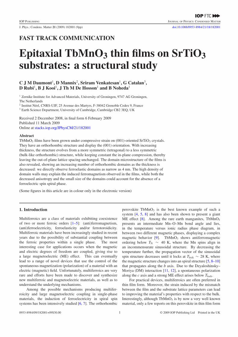
Figure 1. (a) Intensity of the specular spot of the RHEED pattern as a function of deposition time. The inset is a blow-up of the first RHEEDoscillation showing the laser pulses. (b) Typical RHEED pattern obtained after growth and annealing. The picture is taken after cooling downto room temperature and under vacuum. (c) and (d) AFM images of a 2 and 8 nm thin film, respectively, grown at pO2 = 0.25 mbar. Thevertical and horizontal scales are shown at the bottom of the pictures.
are available [13–15]. Since the magnetic and ferroelectricphases are determined by the crystal structure, a thoroughcharacterization of the structure of the films is needed. This,however, is not straightforward due to the small thickness ofthe films and grazing incidence diffraction, using synchrotronsources, is required. In this work, we present the growth andstructural characterization of TbMnO3 perovskite thin filmswith thicknesses lower than 100 nm on single crystals of (001)-SrTiO3. (001)-SrTiO3 is preferred in studies of epitaxy inperovskites because it can be obtained with atomically flatsurfaces, favoring high quality growth. The films are shown tobe very flat, c-oriented and epitaxially strained. Their unit cellis orthorhombic with an orthorhombic distortion that can betuned with the film thickness up to a thickness of about 50 nm.
Although ferroelectric and magnetoelectric measurementsare still in progress, the magnetic properties (reportedelsewhere [14]) suggest that these films are remarkablydifferent from the bulk material: no evidence of thespiral spin structure that gives rise to multiferroic behaviorwas found in the magnetic data. On the other hand,ferromagnetic interactions are induced in the films, which
renders them appealing for applications such as spin valves,where ferromagnetic insulators are required. This is inagreement with a very recent work on the same system [15] andreports in other orthorhombic manganite films [16]. We showhere that the structure of the films and microstructure are likelyto explain the difference between the film and bulk behavior.
2. Experimental details
(001)-oriented TbMnO3 (TMO) thin films were depositedon (001)-SrTiO3 (STO) substrates by pulsed laser deposition(PLD) assisted by reflective high energy electron diffraction(RHEED), using a KrF excimer laser with λ = 248 nm. Astoichiometric target of TbMnO3 was prepared by means of astandard solid-state reaction. Prior to deposition, the substrateswere chemically treated and fired in O2 in order to obtain TiO2
single-terminated flat terraces [17]. The deposition of the filmsreported here was performed at 750 ◦C in oxygen pressuresof 0.25–0.9 mbar. The laser fluence was 2 J cm−2, with arepetition rate of 1 Hz, and a distance between substrate andtarget of 55 mm. After deposition, the films were slowly cooled
2
J. Phys.: Condens. Matter 21 (2009) 182001 Fast Track Communication
0
-2
-4
-6
Inte
nsity
(a.
u.)
0
-2
-4
-6
Inte
nsity
(a.
u.)
0
-2
-4
-6
Inte
nsity
(a.
u.)
11.0 11.5 12.0 12.5 13.0 11.0 11.5 12.0 12.5 13.0 11.0 11.5 12.0 12.5 13.02θ/2 (deg) 2θ/2 (deg) 2θ/2 (deg)
(a) (b) (c)
200 nm 200 nm200 nm
3.49 nm 8.57 nm 13.51 nm
0.00 nm 0.00 nm 0.00 nm
(d) (e) (f)
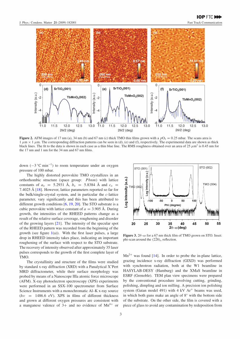
Figure 2. AFM images of 17 nm (a), 34 nm (b) and 67 nm (c) thick TMO thin films grown with a pO2 = 0.25 mbar. The scans area is1 μm × 1 μm. The corresponding diffraction patterns can be seen in (d), (e) and (f), respectively. The experimental data are shown as thickblack lines. The fit to the data is shown in each case as a thin blue line. The RMS roughness obtained over an area of 25 μm2 is 0.45 nm forthe 17 nm and 1 nm for the 34 nm and 67 nm films.
down (−3 ◦C min−1) to room temperature under an oxygenpressure of 100 mbar.
The highly distorted perovskite TMO crystallizes in anorthorhombic structure (space group: Pbnm) with latticeconstants of ao = 5.2931 A, bo = 5.8384 A and co =7.4025 A [18]. However, lattice parameters reported so far forthe bulk/single-crystal system, and in particular the c-latticeparameter, vary significantly and this has been attributed todifferent growth conditions [6, 19, 20]. The STO substrate is acubic perovskite with lattice constant of a = 3.905 A. Duringgrowth, the intensities of the RHEED patterns change as aresult of the relative surface coverage, roughening and disorderof the growing layers [21]. The intensity of the specular spotof the RHEED pattern was recorded from the beginning of thegrowth (see figure 1(a)). With the first laser pulses, a largedrop in RHEED intensity takes place, indicating an importantroughening of the surface with respect to the STO substrate.The recovery of intensity observed after approximately 35 laserpulses corresponds to the growth of the first complete layer ofTMO.
The crystallinity and structure of the films were studiedby standard x-ray diffraction (XRD) with a Panalytical X’PertMRD diffractometer, while their surface morphology wasprobed by means of a Nanoscope IIIa atomic force microscope(AFM). X-ray photoelectron spectroscopy (XPS) experimentswere performed in an SSX-100 spectrometer from SurfaceScience Instruments with a monochromatic Al–K x-ray source(hν = 1486.6 eV). XPS in films of different thicknessand grown at different oxygen pressures are consistent witha manganese valence of 3+ and no evidence of Mn4+ or
Figure 3. 2θ–ω for a 67 nm thick film of TMO grown on STO. Inset:phi-scan around the (228)o reflection.
Mn2+ was found [14]. In order to probe the in-plane lattice,grazing incidence x-ray diffraction (GIXD) was performedwith synchrotron radiation, both at the W1 beamline inHASYLAB-DESY (Hamburg) and the XMaS beamline inESRF (Grenoble). TEM plan view specimens were preparedby the conventional procedure involving cutting, grinding,polishing, dimpling and ion milling. A precision ion polishingsystem (Gatan model 491) with 4 kV Ar+ beams was used,in which both guns make an angle of 8◦ with the bottom sideof the substrate. On the other side, the film is covered with apiece of glass to avoid any contamination by redeposition from
3
J. Phys.: Condens. Matter 21 (2009) 182001 Fast Track Communication
Figure 4. Reciprocal space maps around the (103)c Bragg reflection of the STO substrate for 17, 34 and 67 nm films grown at 0.25 mbar. Thevertical and horizontal lines are guides to the eyes. The abscissa (ordinate) represents the in-plane (out-of-plane) component of the scatteringvector. Both are normalized by 2ko = 4π/λ.
Figure 5. (a) RSM around (206)o and (026)o for a 67 nm thick TMO film grown at 0.25 mbar. The arrow indicates the kpar of the STOsubstrate. (b) RSM around the (103)c STO Bragg reflection for an 80 nm thick TMO film grown at 0.9 mbar. The abscissa (ordinate)represents the in-plane (out-of-plane) component of the scattering vector, both normalized by 2ko = 4π/λ.
the sputtered backside. The observations have been performedwith a JEOL 2010F electron microscope at an acceleratingvoltage of 200 kV.
3. Results
About eight RHEED intensity oscillations can be seen at thebeginning of the growth corresponding to an initial layer-by-layer (2D-like) growth. However, those oscillations aresuperimposed on a decreasing intensity background, indicatingthat an overall roughening occurs as the growth proceeds.After the oscillations have faded away and the intensity of thespecular spot has decreased to a certain intensity, the latterremains constant during the rest of the deposition (outside ofthe graph range) and the pattern changes from a purely stripypattern to the mixed stripe–spot pattern shown in figure 1(b).This type of behavior has been reported recently for otheroxides as a ‘pseudo-2D island growth’ [22, 23]. This changefrom 2D character to ‘pseudo’-3D character of the growth hasalso been identified using AFM. Indeed, figure 1(c) shows themorphology of a 2 nm film, for which the deposition wasstopped shortly before the 2D-to-3D transition. It can be seenthat the film is atomically flat, showing the step-and-terracemorphology of the substrate. However, when the depositionis stopped at the initial stage of the transition from 2D to
3D growth, particles with a diameter of around 30 nm startappearing, as shown in figure 1(d). We found that the changefrom 2D to 3D growth occurs at a thickness in between 2 and5 nm.
Figures 2(a)–(c) show AFM images of three TMO filmswith different thicknesses grown under the same conditions.In the 17 nm film (figure 2(a)), although it is already inthe 3D growth regime and the grains dominate the filmmorphology, the steps from the substrate are still visible. Thesteps are not clearly visible for a 34 nm and 67 nm film(figures 2(b) and (c)). Figures 2(d)–(f) show typical 2θ–ω
x-ray diffractograms around the (001)c Bragg reflection ofSTO (the most intense ones in the pattern), for the same threefilms. The film peaks are those on the right-hand side ofthe STO reflections. The blue lines are the fits of the crystaltruncation rod using a kinematical model. These calculationstake into account, not only the complex refractive index ofthe substrate and the film, but also the angular-dependentatomic scattering factors. The high quality and flatness of theinterfaces is evidenced by the Laue fringes around the film peakfor thicknesses up to 67 nm.
Figure 3 shows a broader 2θ–ω scan including both the(001)c and the (002)c STO Bragg reflections. No secondaryor impurity phases could be observed. A phi-scan aroundthe (024)pc (i.e. (228)o) of TMO (see the inset) shows the
4
J. Phys.: Condens. Matter 21 (2009) 182001 Fast Track Communication
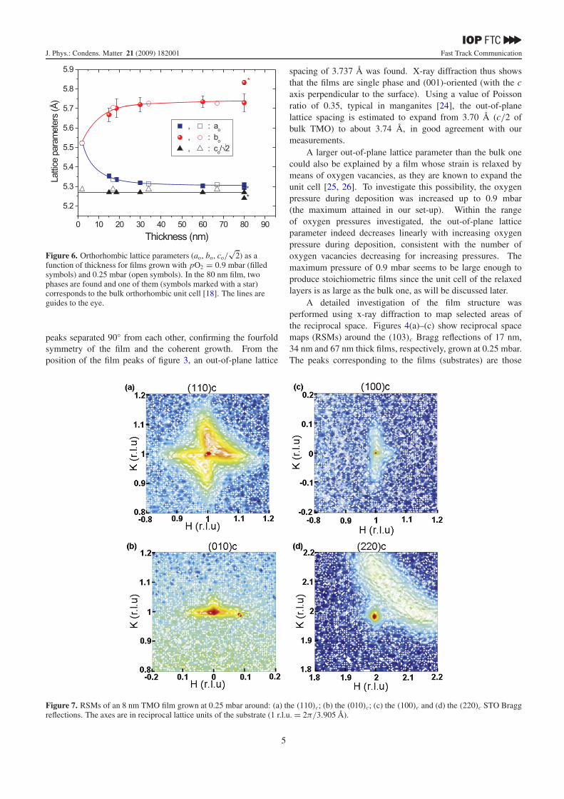
Figure 6. Orthorhombic lattice parameters (ao, bo, co/√
2) as afunction of thickness for films grown with pO2 = 0.9 mbar (filledsymbols) and 0.25 mbar (open symbols). In the 80 nm film, twophases are found and one of them (symbols marked with a star)corresponds to the bulk orthorhombic unit cell [18]. The lines areguides to the eye.
peaks separated 90◦ from each other, confirming the fourfoldsymmetry of the film and the coherent growth. From theposition of the film peaks of figure 3, an out-of-plane lattice
spacing of 3.737 A was found. X-ray diffraction thus showsthat the films are single phase and (001)-oriented (with the caxis perpendicular to the surface). Using a value of Poissonratio of 0.35, typical in manganites [24], the out-of-planelattice spacing is estimated to expand from 3.70 A (c/2 ofbulk TMO) to about 3.74 A, in good agreement with ourmeasurements.
A larger out-of-plane lattice parameter than the bulk onecould also be explained by a film whose strain is relaxed bymeans of oxygen vacancies, as they are known to expand theunit cell [25, 26]. To investigate this possibility, the oxygenpressure during deposition was increased up to 0.9 mbar(the maximum attained in our set-up). Within the rangeof oxygen pressures investigated, the out-of-plane latticeparameter indeed decreases linearly with increasing oxygenpressure during deposition, consistent with the number ofoxygen vacancies decreasing for increasing pressures. Themaximum pressure of 0.9 mbar seems to be large enough toproduce stoichiometric films since the unit cell of the relaxedlayers is as large as the bulk one, as will be discussed later.
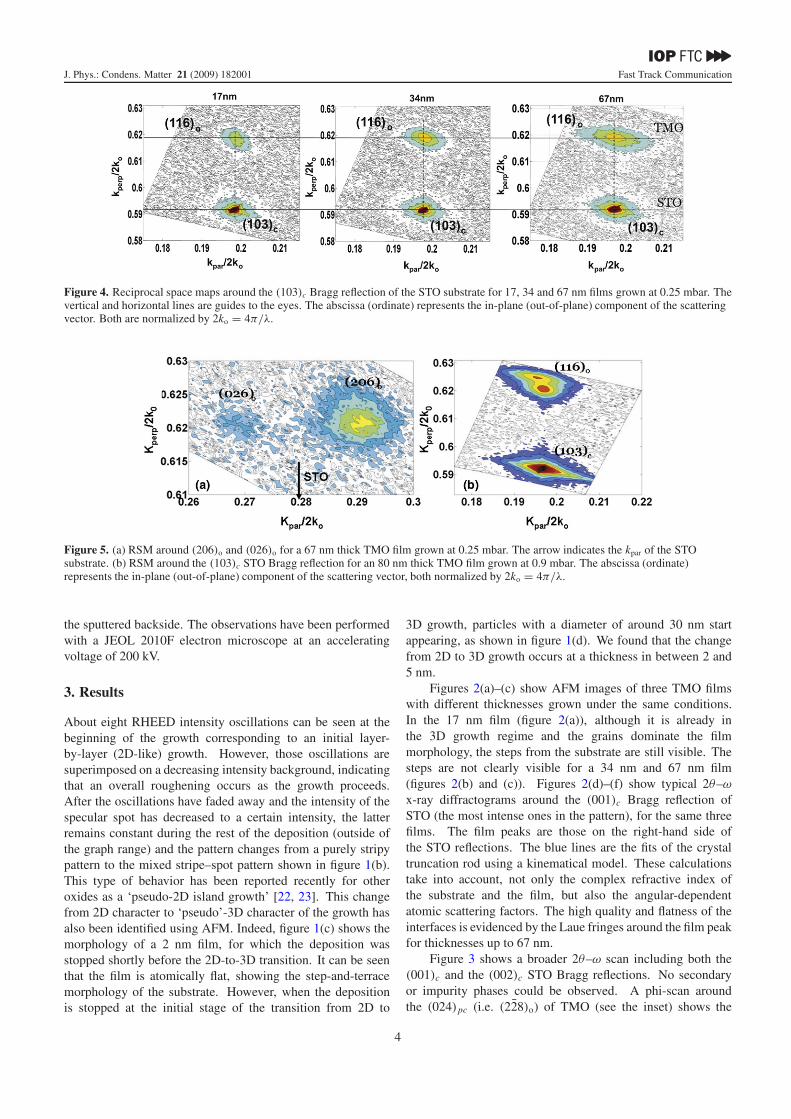
A detailed investigation of the film structure wasperformed using x-ray diffraction to map selected areas ofthe reciprocal space. Figures 4(a)–(c) show reciprocal spacemaps (RSMs) around the (103)c Bragg reflections of 17 nm,34 nm and 67 nm thick films, respectively, grown at 0.25 mbar.The peaks corresponding to the films (substrates) are those
Figure 7. RSMs of an 8 nm TMO film grown at 0.25 mbar around: (a) the (110)c; (b) the (010)c; (c) the (100)c and (d) the (220)c STO Braggreflections. The axes are in reciprocal lattice units of the substrate (1 r.l.u. = 2π/3.905 A).
5
J. Phys.: Condens. Matter 21 (2009) 182001 Fast Track Communication
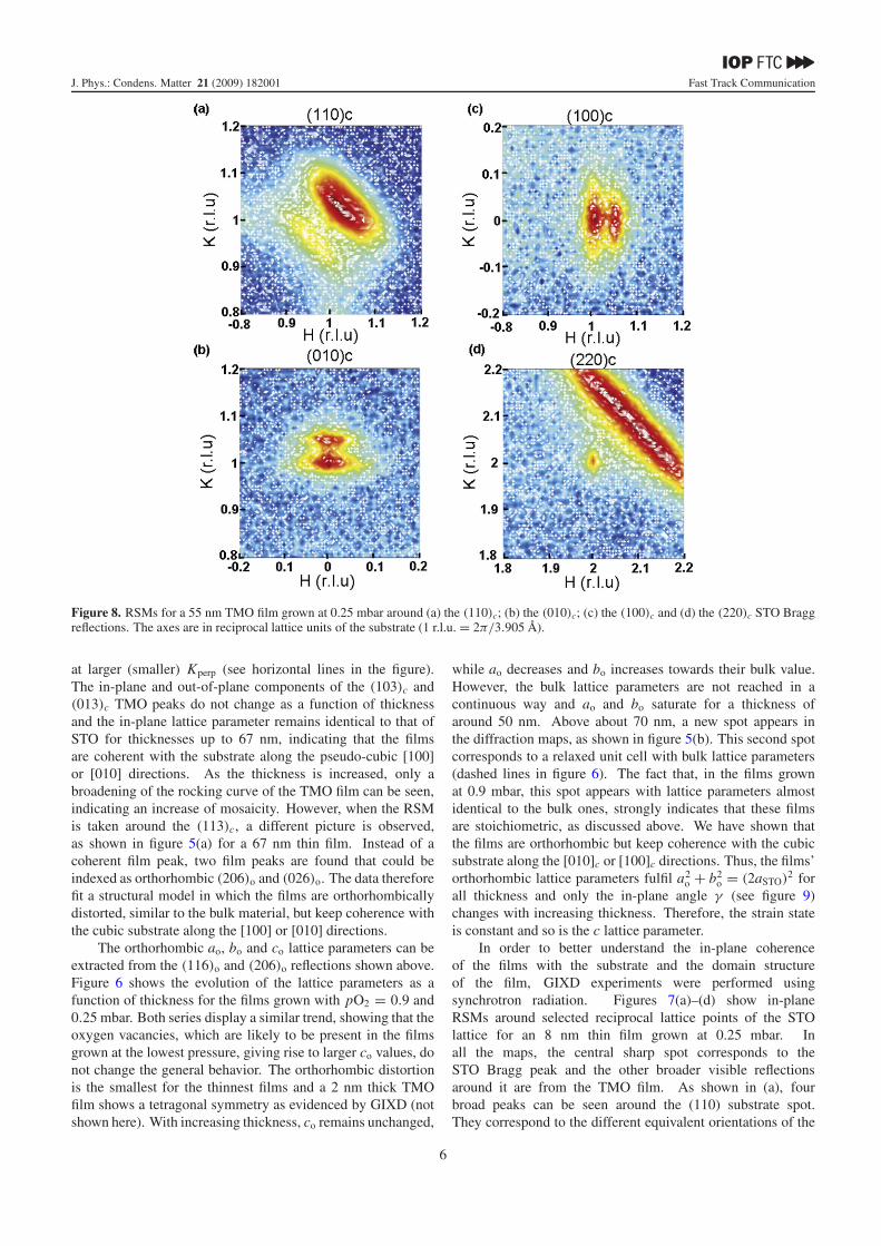
Figure 8. RSMs for a 55 nm TMO film grown at 0.25 mbar around (a) the (110)c; (b) the (010)c; (c) the (100)c and (d) the (220)c STO Braggreflections. The axes are in reciprocal lattice units of the substrate (1 r.l.u. = 2π/3.905 A).
at larger (smaller) Kperp (see horizontal lines in the figure).The in-plane and out-of-plane components of the (103)c and(013)c TMO peaks do not change as a function of thicknessand the in-plane lattice parameter remains identical to that ofSTO for thicknesses up to 67 nm, indicating that the filmsare coherent with the substrate along the pseudo-cubic [100]or [010] directions. As the thickness is increased, only abroadening of the rocking curve of the TMO film can be seen,indicating an increase of mosaicity. However, when the RSMis taken around the (113)c, a different picture is observed,as shown in figure 5(a) for a 67 nm thin film. Instead of acoherent film peak, two film peaks are found that could beindexed as orthorhombic (206)o and (026)o. The data thereforefit a structural model in which the films are orthorhombicallydistorted, similar to the bulk material, but keep coherence withthe cubic substrate along the [100] or [010] directions.
The orthorhombic ao, bo and co lattice parameters can beextracted from the (116)o and (206)o reflections shown above.Figure 6 shows the evolution of the lattice parameters as afunction of thickness for the films grown with pO2 = 0.9 and0.25 mbar. Both series display a similar trend, showing that theoxygen vacancies, which are likely to be present in the filmsgrown at the lowest pressure, giving rise to larger co values, donot change the general behavior. The orthorhombic distortionis the smallest for the thinnest films and a 2 nm thick TMOfilm shows a tetragonal symmetry as evidenced by GIXD (notshown here). With increasing thickness, co remains unchanged,
while ao decreases and bo increases towards their bulk value.However, the bulk lattice parameters are not reached in acontinuous way and ao and bo saturate for a thickness ofaround 50 nm. Above about 70 nm, a new spot appears inthe diffraction maps, as shown in figure 5(b). This second spotcorresponds to a relaxed unit cell with bulk lattice parameters(dashed lines in figure 6). The fact that, in the films grownat 0.9 mbar, this spot appears with lattice parameters almostidentical to the bulk ones, strongly indicates that these filmsare stoichiometric, as discussed above. We have shown thatthe films are orthorhombic but keep coherence with the cubicsubstrate along the [010]c or [100]c directions. Thus, the films’orthorhombic lattice parameters fulfil a2
o + b2o = (2aSTO)2 for
all thickness and only the in-plane angle γ (see figure 9)changes with increasing thickness. Therefore, the strain stateis constant and so is the c lattice parameter.
In order to better understand the in-plane coherenceof the films with the substrate and the domain structureof the film, GIXD experiments were performed usingsynchrotron radiation. Figures 7(a)–(d) show in-planeRSMs around selected reciprocal lattice points of the STOlattice for an 8 nm thin film grown at 0.25 mbar. Inall the maps, the central sharp spot corresponds to theSTO Bragg peak and the other broader visible reflectionsaround it are from the TMO film. As shown in (a), fourbroad peaks can be seen around the (110) substrate spot.They correspond to the different equivalent orientations of the
6
J. Phys.: Condens. Matter 21 (2009) 182001 Fast Track Communication
apc
ao
bo
(a) (b)
(c) (d)
apc
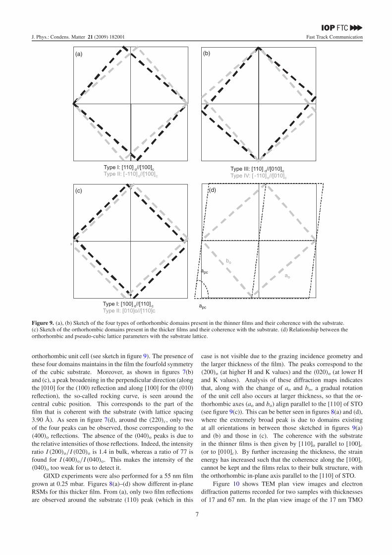
Figure 9. (a), (b) Sketch of the four types of orthorhombic domains present in the thinner films and their coherence with the substrate.(c) Sketch of the orthorhombic domains present in the thicker films and their coherence with the substrate. (d) Relationship between theorthorhombic and pseudo-cubic lattice parameters with the substrate lattice.
orthorhombic unit cell (see sketch in figure 9). The presence ofthese four domains maintains in the film the fourfold symmetryof the cubic substrate. Moreover, as shown in figures 7(b)and (c), a peak broadening in the perpendicular direction (alongthe [010] for the (100) reflection and along [100] for the (010)reflection), the so-called rocking curve, is seen around thecentral cubic position. This corresponds to the part of thefilm that is coherent with the substrate (with lattice spacing3.90 A). As seen in figure 7(d), around the (220)c, only twoof the four peaks can be observed, those corresponding to the(400)o reflections. The absence of the (040)o peaks is due tothe relative intensities of those reflections. Indeed, the intensityratio I (200)o/I (020)o is 1.4 in bulk, whereas a ratio of 77 isfound for I (400)o/I (040)o. This makes the intensity of the(040)o too weak for us to detect it.
GIXD experiments were also performed for a 55 nm filmgrown at 0.25 mbar. Figures 8(a)–(d) show different in-planeRSMs for this thicker film. From (a), only two film reflectionsare observed around the substrate (110) peak (which in this
case is not visible due to the grazing incidence geometry andthe larger thickness of the film). The peaks correspond to the(200)o (at higher H and K values) and the (020)o (at lower Hand K values). Analysis of these diffraction maps indicatesthat, along with the change of ao and bo, a gradual rotationof the unit cell also occurs at larger thickness, so that the or-thorhombic axes (ao and bo) align parallel to the [110] of STO(see figure 9(c)). This can be better seen in figures 8(a) and (d),where the extremely broad peak is due to domains existingat all orientations in between those sketched in figures 9(a)and (b) and those in (c). The coherence with the substratein the thinner films is then given by [110]o parallel to [100]c
(or to [010]c). By further increasing the thickness, the strainenergy has increased such that the coherence along the [100]c
cannot be kept and the films relax to their bulk structure, withthe orthorhombic in-plane axis parallel to the [110] of STO.
Figure 10 shows TEM plan view images and electrondiffraction patterns recorded for two samples with thicknessesof 17 and 67 nm. In the plan view image of the 17 nm TMO
7

J. Phys.: Condens. Matter 21 (2009) 182001 Fast Track Communication
17 nm 67 nm
Figure 10. Plan view TEM pictures of a 17 nm (a) and 67 nm (b) TMO film. Electron diffraction patterns of the same films are shown in (c)and (d), respectively. The white circles show the presence of dislocations.
film, two differently oriented types of rectangular domainscan be seen along with strain contrast for domains having thesame orientation. This is consistent with the four types ofdomains seen via XRD. For the thicker film, two orientationscan still be seen along with bigger domains, consistentwith the coalescence of the grains seen by AFM. Moreover,strain contrast is present within the domains, showing thatthe domains coalesce as the thickness increases. Screwdislocations can be seen on the thicker film. In additionto screw dislocations at the interface, another type of defectprobably exists at the domain boundaries that take care ofthe in-plane rotation of the domains. The electron diffractionpatterns confirm what has been seen in x-ray diffraction: for thethinner film, the diffraction peaks are the superposition of fourTMO domains along with the contribution from the substrate;for the 67 nm TMO thin film, the electron diffraction patterndiffers from that of the very thin films and shows a rotationgradient, as discussed above.
4. Discussion
For the 17 nm film, the domains are found to have a smallwidth of about 4 nm (see figure 10(a)). This domain size isparticularly small when compared with the typical thicknessof magnetic domain walls, which are of the order of severalnanometers [27, 28]. This means that in the thin filmsthe fraction occupied by domain walls is comparable to thatof the domains themselves, and therefore the properties of
the domain walls are likely to affect the overall magneticproperties, that is, the induced weak ferromagnetism, andperhaps even the absence of a lock-in transition [14]. Forexample, while the orthorhombic domains are known to beantiferromagnetic in character, in agreement with the negativeCurie–Weiss temperature measured in the films [14], themagnetic interactions at the domain walls can give rise to aferromagnetic component. Symmetry arguments show thatmagnetoelectric coupling can induce ferromagnetism in thedomain walls of ferroelectric antiferromagnets [29], and worksby Fiebig and co-workers have also shown that the ferroelectricdomain walls of multiferroic hexagonal manganites can havea net magnetization at their center [30] as well as enhancedmagnetoelectric coupling [31].
The small domain size is likely to also affect the spinspiral. In bulk TbMnO3, the period of the spiral is of the orderof 2 nm, which is comparable to the domain size and so it maywell be destroyed by the proximity of the domain boundaries.Moreover, even if the spiral spin order that gives rise to thelock-in and ferroelectric transition survived, the domain sizemay be incommensurate with the spiral period, meaning thatsome spins will not be fully compensated, an effect that willbe more noticeable for smaller domains. The presence of smalldomains would also prevent long range coherence, since thespiral propagation direction, which is along the orthorhombicb axis, has to flick from the x to y directions at each domainwall.
Finally, the reduction of in-plane anisotropy means thatthe difference between the a and b lattice parameters in the
8
J. Phys.: Condens. Matter 21 (2009) 182001 Fast Track Communication
orthorhombic structure decreases. For the extreme case of thetetragonal films (2 nm thick or less) there is no privilegeddirection, and hence there can be no spin spiral. But evenfor the thicker orthorhombic films, strain is likely to affect,or even destroy, the spin spiral, since the changes in in-planeanisotropy with respect to the bulk compound must also affectthe Mn–O–Mn bond angle, which is known to be the criticalparameter for the appearance of the lock-in spiral phase [32].
5. Concluding remarks
We have successfully deposited epitaxial orthorhombicTbMnO3 films on (001)-SrTiO3, with thicknesses ranging from8 to 80 nm. The crystal structure of the thin strained filmshas been identified as a less distorted orthorhombic unit cellcompared to the bulk one with afilm > abulk, bfilm < bbulk
and cfilm > cbulk. We found that the films grow with thec axis out of plane and they orient themselves in the planesuch that the 〈110〉o directions align with the 〈100〉c directionsof the substrate. The orthorhombic lattice parameters ao andbo are constrained by epitaxy so that a2
o + b2o = (2aSTO)2.
This allows for four equivalent orientations and, therefore,four types of domains are observed, such that the in-planediffraction patterns display fourfold symmetry.
With increasing thickness, the in-plane orthorhombic axesgradually change towards their bulk values, increasing theorthorhombicity of the films, but still keeping the partialcoherence and epitaxy relation a2
o + b2o = (2aSTO)2. Due
to this, the amount of in-plane compression (and hence out-of-plane elongation) remains unchanged up to thicknesses ofabout 70 nm. Above this thickness, the lattice relaxes to thebulk one. In spite of the unchanged in-plane compression,the thicker films do show a distribution of unit cell rotationscoupled with increasing orthorhombic distortion.
It has been shown [14] that the physical properties of thesefilms are very different from those of the bulk: the films showferromagnetic interactions and spin-glass-like behavior belowthe Neel temperature of ∼40 K, which are absent in the bulk.This can be of interest due to the scarcity of ferromagneticinsulators. Similar results have recently been obtained for thisand other orthorhombic perovskites [15, 16]. Here, we proposethat this is directly associated with the domain walls, showingevidence that these constitute a large part of the volume of thefilms. On the other hand, the magnetic anomaly observed inthe bulk material at about 28 K, related to the transition tothe spiral spin structure and the onset of ferroelectricity, couldnot be observed in these films [14]. This may be due to the
decrease of in-plane anisotropy that we show takes place withdecreasing thickness, or to the small domain size. Work is inprogress to investigate these possibilities.
Acknowledgments
The authors would like to thank Umut Adem, Graeme Blake,Claire Colin, Maxim Mostovoy, Mufti Nandang, GwilhermNenert, Thom Palstra, Gijsbert Rispens, Oliver Seeck and ArdVlooswijk for useful discussions and, very specially, HenkBruinenberg, for his invaluable technical support. Finally,financial support by the EU STREP project MaCoMuFi (FP6-03321) is gratefully acknowledged.
References
[1] Hill N A et al 2000 J. Phys. Chem. B 104 6694[2] Fiebig M et al 2005 J. Phys. D: Appl. Phys. 38 R123[3] Eerenstein W et al 2006 Nature 442 759[4] Tokura Y et al 2006 Science 312 1481[5] Tokura Y et al 2007 J. Magn. Magn. Mater. 310 1145[6] Kenzelmann M et al 2005 Phys. Rev. Lett. 95 087206[7] Mostovoy M et al 2006 Phys. Rev. Lett. 96 067601[8] Kajimoto R et al 2004 Phys. Rev. B 70 012401[9] Goto T et al 2004 Phys. Rev. Lett. 92 257201
[10] Kimura T et al 2003 Nature 426 55[11] Sergienko I A et al 2006 Phys. Rev. B 73 094434[12] Malashevich A et al 2008 Phys. Rev. Lett. 101 037210[13] Cui Y et al 2005 Solid State Commun. 133 641[14] Rubi D et al 2009 Phys. Rev. B 79 144416[15] Kirby B J et al 2008 arXiv:0811.4430[16] Marti X et al 2007 arXiv:cond-mat/0701387[17] Koster G et al 1998 Appl. Phys. Lett. 73 2920–2[18] Alonso J A et al 2000 Inorg. Chem. 39 917[19] Blasco J et al 2000 Phys. Rev. B 62 5609[20] Aliouane N et al 2006 Phys. Rev. B 73 020102[21] Ichimiya A and Cohen P I 2004 Reflection High-Energy
Electron Diffraction (Cambridge: Cambridge UniversityPress)
[22] Shin J et al 2007 Appl. Phys. Lett. 91 202901[23] Daudin B et al 1997 Mater. Sci. Eng. B 50 8[24] Ranno L et al 2002 Appl. Surf. Sci. 188 170[25] Babei M and Ross D K 2005 Physica C 425 130[26] Rudman D A et al 1999 IEEE Trans. Appl. Supercond.
9 2460–4[27] Hubert A and Schafer R 1998 Magnetic Domains
(Berlin: Springer)[28] Catalan G et al 2007 J. Phys.: Condens. Matter 19 022201[29] Privratska J and Janovec V 1997 Ferroelectrics 204 321
Privratska J and Janovec V 1999 Ferroelectrics 222 23[30] Goltsev A V et al 2003 Phys. Rev. Lett. 90 177204[31] Lottermoser T and Fiebig M 2004 Phys. Rev. B 70 220407(R)[32] Kimura T et al 2003 Phys. Rev. B 68 060403(R)
9