engin112 f06 final solutions
TRANSCRIPT

7/27/2019 ENGIN112 F06 Final Solutions
http://slidepdf.com/reader/full/engin112-f06-final-solutions 1/14
1
ENGIN 112
Final ExamFall 2006
Prof. Ciesielski / Prof. Wolf
Name: ____________________________________________________
ID Number: ____________________________________________________
This exam is closed book, closed notes. No calculators or other electronic devices allowed. Be
concise, but show your work. Write legibly! Unreadable answers will not be graded.
Time: 120 minutes.
Maximum Achieved
Question 1 26
Question 2 20
Question 3 12
Question 4 13
Question 5 15
Question 6 14
Total 100
7/27/2019 ENGIN112 F06 Final Solutions
http://slidepdf.com/reader/full/engin112-f06-final-solutions 2/14
2
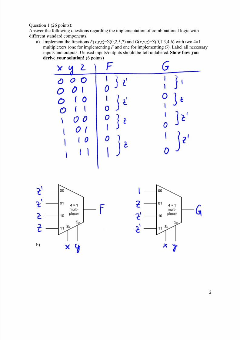
Question 1 (26 points):
Answer the following questions regarding the implementation of combinational logic withdifferent standard components.
a) Implement the functions F ( x, y, z)=Σ(0,2,5,7) and G( x, y, z)=Σ(0,1,3,4,6) with two 4×1multiplexers (one for implementing F and one for implementing G). Label all necessary
inputs and outputs. Unused inputs/outputs should be left unlabeled. Show how you
derive your solution! (6 points)
b)

7/27/2019 ENGIN112 F06 Final Solutions
http://slidepdf.com/reader/full/engin112-f06-final-solutions 3/14
3
Implement the functions F ( x, y, z)=Σ(0,2,5,7) and G( x, y, z)=Σ(0,1,3,4,6) (same as in a))
with the ROM shown below. Mark intact fuses with ‘•’ or ‘×’. Label all necessary
outputs. Unused outputs should be left unlabeled. (4 points)
3 × 8
decoder
z
y
x
D0
D7
I0
I2
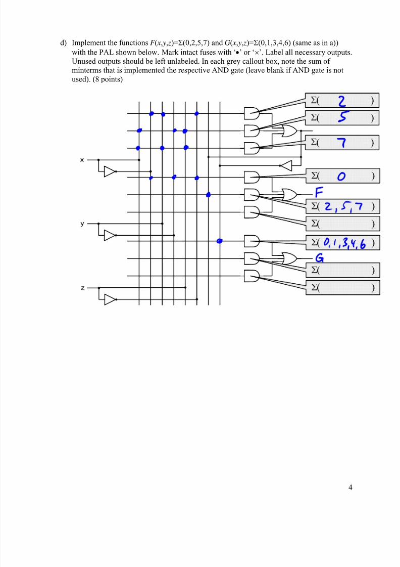
c) Implement the functions F ( x, y, z)=Σ(0,2,5,7) and G( x, y, z)=Σ(0,1,3,4,6) (same as in a))
with the PLA shown below. Mark intact fuses with ‘•’ or ‘×’. Label all necessary outputs.Unused outputs should be left unlabeled. In each grey callout box, note the sum of
minterms that is implemented the respective AND gate (leave blank if AND gate is notused). (8 points)
0
1
z
y
x
7/27/2019 ENGIN112 F06 Final Solutions
http://slidepdf.com/reader/full/engin112-f06-final-solutions 4/14
4
d) Implement the functions F ( x, y, z)=Σ(0,2,5,7) and G( x, y, z)=Σ(0,1,3,4,6) (same as in a))
with the PAL shown below. Mark intact fuses with ‘•’ or ‘×’. Label all necessary outputs.
Unused outputs should be left unlabeled. In each grey callout box, note the sum of minterms that is implemented the respective AND gate (leave blank if AND gate is not
used). (8 points)
7/27/2019 ENGIN112 F06 Final Solutions
http://slidepdf.com/reader/full/engin112-f06-final-solutions 5/14
5
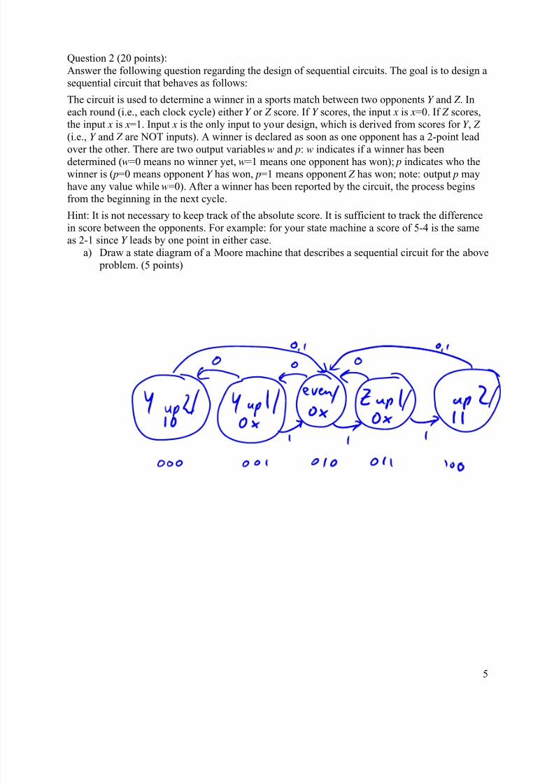
Question 2 (20 points):
Answer the following question regarding the design of sequential circuits. The goal is to design asequential circuit that behaves as follows:
The circuit is used to determine a winner in a sports match between two opponents Y and Z . In
each round (i.e., each clock cycle) either Y or Z score. If Y scores, the input x is x=0. If Z scores,the input x is x=1. Input x is the only input to your design, which is derived from scores for Y , Z
(i.e., Y and Z are NOT inputs). A winner is declared as soon as one opponent has a 2-point lead over the other. There are two output variables w and p: w indicates if a winner has been
determined (w=0 means no winner yet, w=1 means one opponent has won); p indicates who thewinner is ( p=0 means opponent Y has won, p=1 means opponent Z has won; note: output p may
have any value while w=0). After a winner has been reported by the circuit, the process beginsfrom the beginning in the next cycle.
Hint: It is not necessary to keep track of the absolute score. It is sufficient to track the difference
in score between the opponents. For example: for your state machine a score of 5-4 is the sameas 2-1 since Y leads by one point in either case.
a) Draw a state diagram of a Moore machine that describes a sequential circuit for the above
problem. (5 points)
7/27/2019 ENGIN112 F06 Final Solutions
http://slidepdf.com/reader/full/engin112-f06-final-solutions 6/14
6
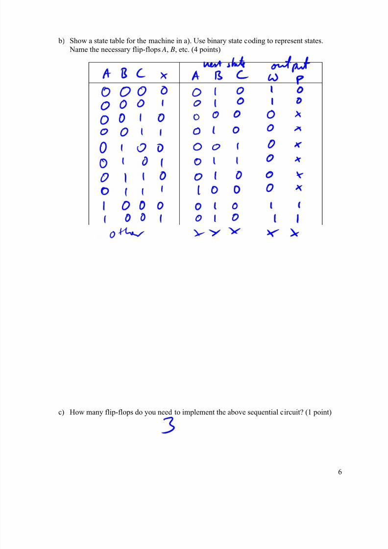
b) Show a state table for the machine in a). Use binary state coding to represent states.
Name the necessary flip-flops A, B, etc. (4 points)
c) How many flip-flops do you need to implement the above sequential circuit? (1 point)

7/27/2019 ENGIN112 F06 Final Solutions
http://slidepdf.com/reader/full/engin112-f06-final-solutions 7/14
7
d) Determine the minimized flip-flop input equation(s) and the minimized output
equation(s). Use Karnaugh maps to minimize equations. Note your solutions in the box below. (10 points)
Flip-flop input equation(s):
Output equation(s):
7/27/2019 ENGIN112 F06 Final Solutions
http://slidepdf.com/reader/full/engin112-f06-final-solutions 8/14
8
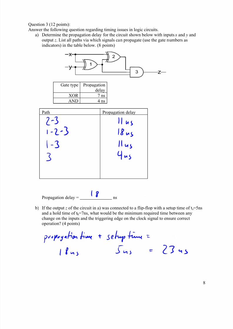
Question 3 (12 points):
Answer the following question regarding timing issues in logic circuits.a) Determine the propagation delay for the circuit shown below with inputs x and y and
output z. List all paths via which signals can propagate (use the gate numbers as
indicators) in the table below. (8 points)
Gate type Propagation
delay
XOR 7 ns
AND 4 ns
Path Propagation delay
Propagation delay = ______________ ns
b) If the output z of the circuit in a) was connected to a flip-flop with a setup time of t s=5ns
and a hold time of th=7ns, what would be the minimum required time between any
change on the inputs and the triggering edge on the clock signal to ensure correctoperation? (4 points)
7/27/2019 ENGIN112 F06 Final Solutions
http://slidepdf.com/reader/full/engin112-f06-final-solutions 9/14
9
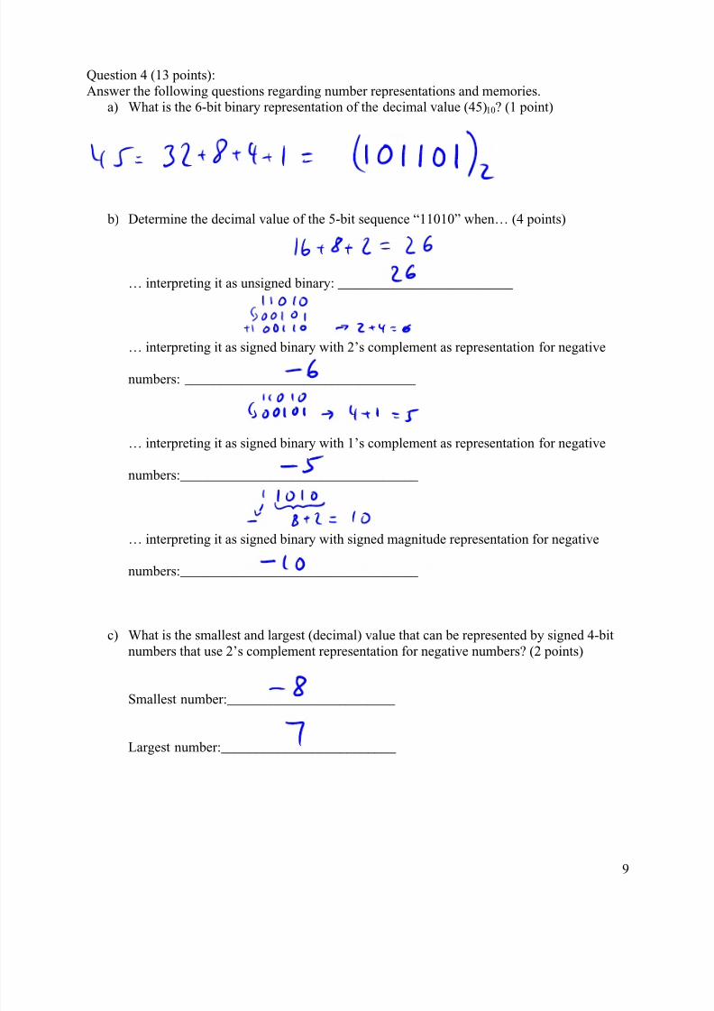
Question 4 (13 points):
Answer the following questions regarding number representations and memories.a) What is the 6-bit binary representation of the decimal value (45)10? (1 point)
b) Determine the decimal value of the 5-bit sequence “11010” when… (4 points)
… interpreting it as unsigned binary: _________________________
… interpreting it as signed binary with 2’s complement as representation for negative
numbers: _________________________________
… interpreting it as signed binary with 1’s complement as representation for negative
numbers:__________________________________
… interpreting it as signed binary with signed magnitude representation for negative
numbers:__________________________________
c) What is the smallest and largest (decimal) value that can be represented by signed 4-bit
numbers that use 2’s complement representation for negative numbers? (2 points)
Smallest number:________________________
Largest number:_________________________
7/27/2019 ENGIN112 F06 Final Solutions
http://slidepdf.com/reader/full/engin112-f06-final-solutions 10/14
10
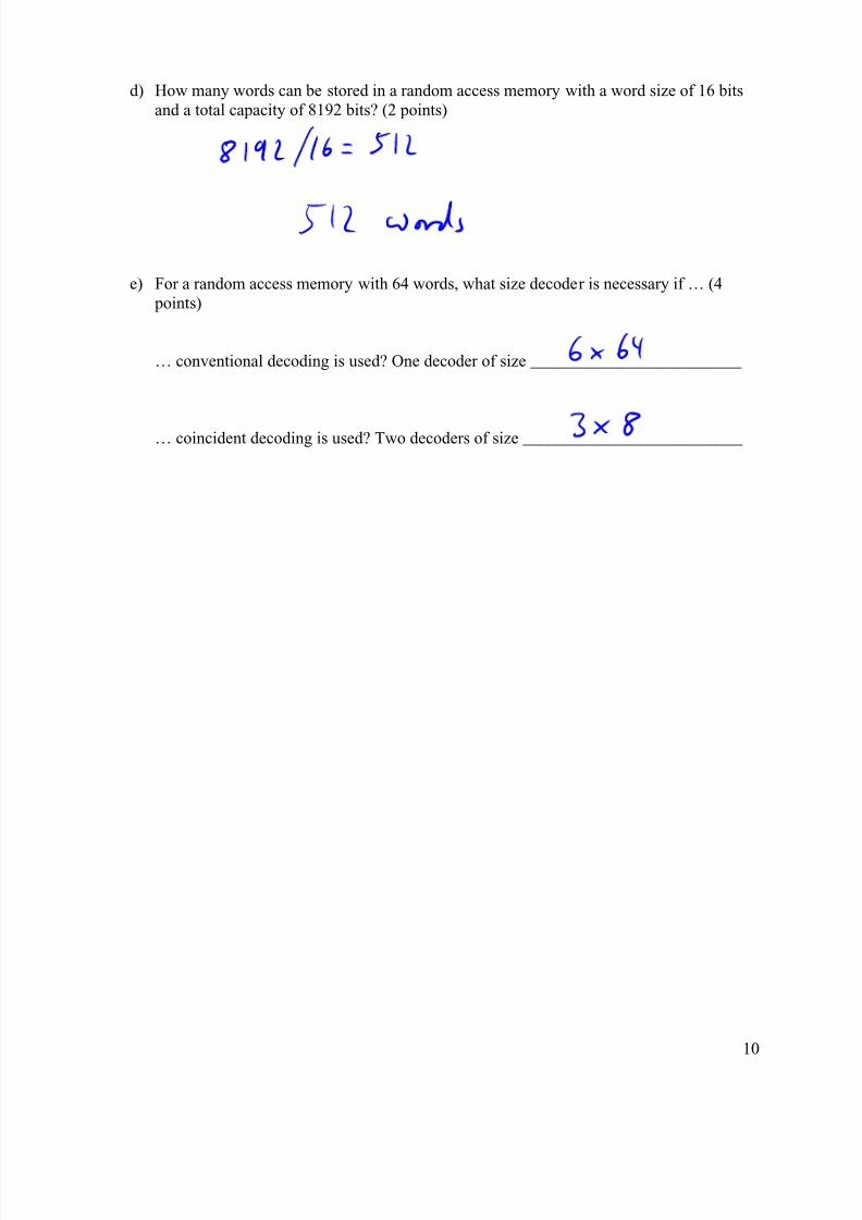
d) How many words can be stored in a random access memory with a word size of 16 bits
and a total capacity of 8192 bits? (2 points)
e) For a random access memory with 64 words, what size decoder is necessary if … (4
points)
… conventional decoding is used? One decoder of size _________________________
… coincident decoding is used? Two decoders of size __________________________
7/27/2019 ENGIN112 F06 Final Solutions
http://slidepdf.com/reader/full/engin112-f06-final-solutions 11/14
11
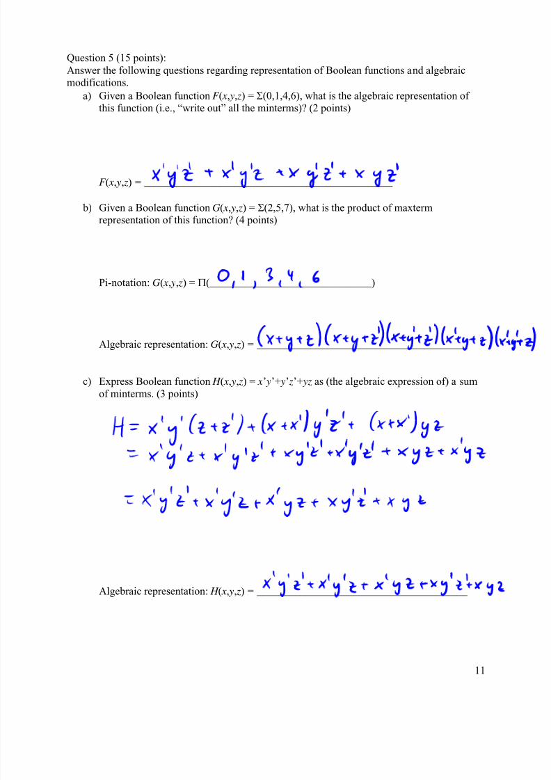
Question 5 (15 points):
Answer the following questions regarding representation of Boolean functions and algebraicmodifications.
a) Given a Boolean function F ( x, y, z) = Σ(0,1,4,6), what is the algebraic representation of this function (i.e., “write out” all the minterms)? (2 points)
F ( x, y, z) = ______________________________________________
b) Given a Boolean function G( x, y, z) = Σ(2,5,7), what is the product of maxtermrepresentation of this function? (4 points)
Pi-notation: G( x, y, z) = Π(______________________________)
Algebraic representation: G( x, y, z) = _______________________________________
c) Express Boolean function H ( x, y, z) = x’ y’+ y’ z’+ yz as (the algebraic expression of) a sum
of minterms. (3 points)
Algebraic representation: H ( x, y, z) = _______________________________________
7/27/2019 ENGIN112 F06 Final Solutions
http://slidepdf.com/reader/full/engin112-f06-final-solutions 12/14
12
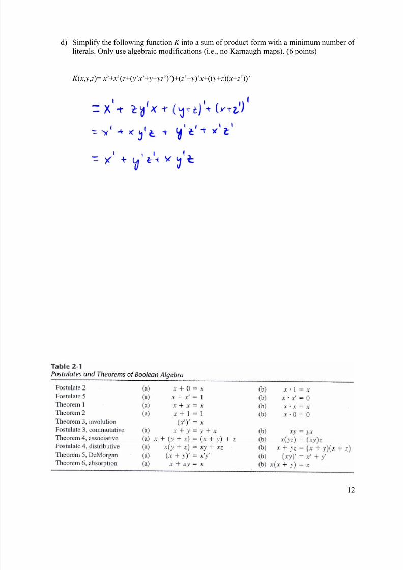
d) Simplify the following function K into a sum of product form with a minimum number of
literals. Only use algebraic modifications (i.e., no Karnaugh maps). (6 points)
K ( x, y, z)= x’+ x’( z+( y’ x’+ y+ yz’)’)+( z’+ y)’ x+(( y+ z)( x+ z’))’
7/27/2019 ENGIN112 F06 Final Solutions
http://slidepdf.com/reader/full/engin112-f06-final-solutions 13/14
13
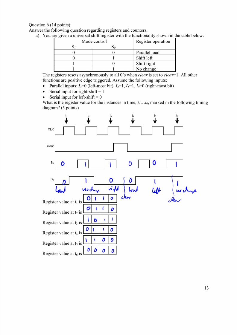
Question 6 (14 points):
Answer the following question regarding registers and counters.a) You are given a universal shift register with the functionality shown in the table below:
Mode control
S1 S0
Register operation
0 0 Parallel load
0 1 Shift left1 0 Shift right
1 1 No change
The registers resets asynchronously to all 0’s when clear is set to clear =1. All other
functions are positive edge triggered. Assume the following inputs:
• Parallel inputs: I 3=0 (left-most bit), I 2=1, I 1=1, I 0=0 (right-most bit)
• Serial input for right-shift = 1
• Serial input for left-shift = 0
What is the register value for the instances in time, t 1…t 6 , marked in the following timing
diagram? (5 points)
CLK
clear
S1
S0
t1
t2
t3
t4
t5
t6
Register value at t1 is
Register value at t2 is
Register value at t3 is
Register value at t4 is
Register value at t5 is
Register value at t6 is

7/27/2019 ENGIN112 F06 Final Solutions
http://slidepdf.com/reader/full/engin112-f06-final-solutions 14/14
14
b) Draw the circuit diagram for a 2-bit ripple counter. The counter should count up on each
positive clock (CLK ) edge if input x is x=1. There is no reset, enable, or other input. Youmay use any logic component and flip flop you want. Indicate the type of any flip-flop
you use. Clearly label the outputs as follows: the least significant counter bit should be
labeled C0, the most significant counter bit should be labeled C1. (5 points)
That’s it. You’re done. Enjoy the holidays!