electron energy loss and diffraction of backscattered...
TRANSCRIPT
Electron energy loss and diffraction of backscattered electrons from silicon
This article has been downloaded from IOPscience. Please scroll down to see the full text article.
2010 New J. Phys. 12 053001
(http://iopscience.iop.org/1367-2630/12/5/053001)
Download details:
IP Address: 150.203.177.172
The article was downloaded on 13/05/2010 at 01:21
Please note that terms and conditions apply.
View the table of contents for this issue, or go to the journal homepage for more
Home Search Collections Journals About Contact us My IOPscience
T h e o p e n – a c c e s s j o u r n a l f o r p h y s i c s
New Journal of Physics
Electron energy loss and diffraction of backscatteredelectrons from silicon
Aimo Winkelmann1,3, Koceila Aizel2 and Maarten Vos2
1 Max-Planck-Institut für Mikrostrukturphysik, Weinberg 2, D-06120 Halle(Saale), Germany2 Research School of Physics and Engineering, Australian National University,Canberra, ACT, AustraliaE-mail: [email protected]
New Journal of Physics 12 (2010) 053001 (18pp)Received 15 February 2010Published 5 May 2010Online at http://www.njp.org/doi:10.1088/1367-2630/12/5/053001
Abstract. Electrons backscattered from crystals can show Kikuchi patterns:variations in intensity for different outgoing directions due to diffraction by thelattice. Here, we measure these effects as a function of their energy loss for30 keV electrons backscattered from silicon. The change in diffraction contrastwith energy loss depends strongly on the scattering geometry. At steep incidenceon the sample, diffraction contrast in the observed Kikuchi bands decreasesrapidly with energy loss. For an energy loss larger than about 150 eV the contrastis more than 5 times less than the contrast due to electrons near zero energyloss. However, for grazing incidence angles, maximum Kikuchi band contrast isobserved for electrons with an energy loss near 60 eV, where the contrast is morethan 2.5× larger than near zero energy loss. In addition, in this grazing incidencegeometry, the Kikuchi diffraction effects stay significant even for electrons thathave lost hundreds of electron volts. For the maximum measured energy lossof 440 eV, the electrons still show a contrast that is 1.5 × larger than that ofthe electrons near zero energy loss. These geometry-dependent observationsof Kikuchi band diffraction contrast are interpreted based on the elastic andinelastic scattering properties of electrons and dynamical diffraction simulations.
3 Author to whom any correspondence should be addressed.
New Journal of Physics 12 (2010) 0530011367-2630/10/053001+18$30.00 © IOP Publishing Ltd and Deutsche Physikalische Gesellschaft
2
Contents
1. Introduction 22. Experimental details 33. Results 4
3.1. Data analysis . . . . . . . . . . . . . . . . . . . . . . . . . . . . . . . . . . . 43.2. Kikuchi band profiles and energy loss . . . . . . . . . . . . . . . . . . . . . . 7
4. Discussion 105. Summary 16Acknowledgments 16References 17
1. Introduction
Spectroscopic energy loss measurements of scattered electrons can provide analytical accessto the physical properties of surfaces. This is due to a variety of possible interactions ofthe probe electrons with the target, such as plasmons, phonon or valence and inner shellexcitations [1]–[4], as well as recoil losses (the transfer of kinetic energy from an electron toa nucleus in a large-angle electron deflection) [5, 6]. For high-resolution reflection energy lossspectroscopy (REELS) with primary electron energies in the order of few tens of keV [7]–[10],diffraction effects are important for crystalline and polycrystalline systems. These diffractioneffects can result in reflection high-energy electron diffraction (RHEED) patterns [11] orKikuchi patterns [12, 13].
Electron diffraction at these energies is increasingly used in practical materialscience applications in scanning electron microscopes (SEM) for local crystallographiccharacterization. A prominent method is electron backscatter diffraction (EBSD) [14]–[18].Closely related to EBSD are the electron channeling patterns (ECP) [19]. The Kikuchi patternsthat are measured in EBSD are fixed to the local crystallographic orientation and thus provide areference for the grain orientation in polycrystalline materials, which is important e.g. for theirmechanical properties.
EBSD patterns are recorded without dedicated energy resolution of the diffracted electrons.A conceptually very simple setup consisting of a phosphor screen and a sensitive CCD camerais used to collect backscattered electrons of all energies over an extended solid angle. For thelarge-angle scattering conditions used in EBSD, practically all elastically scattered electronsare scattered incoherently with respect to the incident beam. Hence, the Kikuchi patterns fromincoherent sources observed in EBSD dominate over the coherent RHEED spot patterns, whichcan only be observed for small scattering angles.
Inelastic scattering leads to a redistribution of electrons over a large energy range, and itis currently not clear what energy range contributes to the diffraction contrast observed in anEBSD pattern. In order to quantitatively understand the pattern formation in EBSD and relatedtechniques, we need more experimental information about the microscopic details of energy andmomentum transfer in order to establish the degree to which coherence of the scattered electronwaves can be sensed after multiple elastic and inelastic events. From a practical point of view,this question is closely linked to the thickness of the crystalline layer that is probed in an actualEBSD measurement, a quantity that is currently not well established.
New Journal of Physics 12 (2010) 053001 (http://www.njp.org/)
3
To investigate this question in a systematic way, it is necessary to do angle-resolvedREELS (or viewed differently: energy-resolved RHEED) at these energies [20]–[22]. Aquantitative correlation between energy loss in REELS experiments and Kikuchi diffractioneffects, however, is experimentally demanding since various spectrometer parameters have to beoptimized at the same time: energy resolution of the order of <1 eV at energies of a few 104 eV,angular acceptance of the order of typical Bragg reflection angles and Kikuchi bandwidths(a few degrees), angular resolution of the order of the width of typical diffraction features(0.1 degree). It has been previously demonstrated how these requirements can be fulfilled byan electrostatic high-energy electron spectrometer [23]–[26].
Here, we present experimental results on the connection between energy loss and diffrac-tion of backscattered electrons from silicon at primary beam energies of 30 keV, building on ourrecent initial investigations [26, 27]. Depending on the experimental geometry, we observe—maybe contrary to intuitive belief—that electrons that have created inelastic excitations canactually show more pronounced diffraction effects than those that are only elastically scattered.The experimental results can be explained using the general features of elastic and inelasticdifferential cross sections at keV energies and arguments from dynamical electron diffractiontheory. We use dynamical electron diffraction simulations to support our analysis.
2. Experimental details
The experimental set up was developed for high-resolution electron momentum spec-troscopy [23]. In the present study, the electrons emitted from gun B were detected for a constantscattering angle of 135.7◦ by a hemispherical electrostatic analyzer that has an energy resolu-tion better than 0.5 eV at 25–40 keV primary beam energy (figures 1 and 2). The diameter of theelectron beam is 0.25 mm.
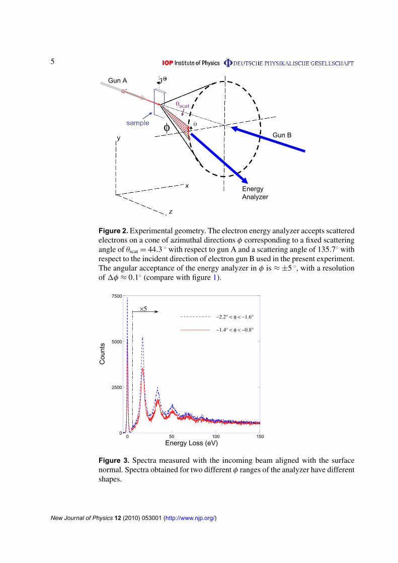
The setup allows angle-resolved detection of electrons on a cone with half-opening angleθscat = 44.3◦, with azimuthal angles φ on that cone in the range of 1φ ≈ ±5◦ (measured fromthe plane given by gun B and the central entrance of the electron energy analyzer, see figure 2).The angular sensitivity is provided by a position-sensitive detector consisting of channel platesand a resistive anode. The position-sensitive detector is calibrated for energy and φ as describedin [23].
In the present experiments, we used primary electron energies of 30 keV and we detectedelectrons with losses of up to 440 eV. We used an Si(001) sample, which was treated by 2 keVXe sputtering and subsequent annealing to more than 900 K by electron beam heating from theback of the sample holder.
The spectra measured show a distinct very intense peak at the low energy loss side. Thisis the elastic peak, and in most of the REELS literature it is assumed to be at zero energy loss.However, for the current kinematic conditions (30 keV e − scattering over 135◦), the kineticenergy transferred from an incident electron to an Si atom is close to 2 eV (recoil loss) [5, 6].As all detected electrons have scattered elastically and thus experienced similar recoil losses,the whole spectrum is shifted by this amount. This small uniform shift does not affect any of theeffects discussed in this paper, and for simplicity we shift the energy scale of the spectra suchthat the elastic peak is at zero energy loss. The relative contribution of the scattering processeswith elastic energy loss to single atoms compared to coherent scattering by the whole crystalcan be estimated from the Debye–Waller factor. For large-angle scattering, the Debye–Wallerfactor is extremely small, quantifying the reduction in coherent scattering from the crystal [28].
New Journal of Physics 12 (2010) 053001 (http://www.njp.org/)
4
High-voltage cage
Gun A
Gun B
Sample
Analyser
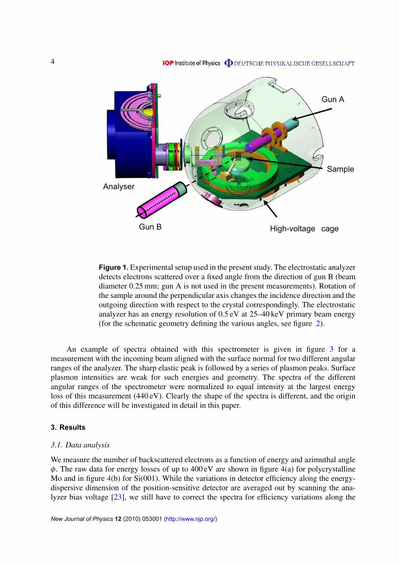
Figure 1. Experimental setup used in the present study. The electrostatic analyzerdetects electrons scattered over a fixed angle from the direction of gun B (beamdiameter 0.25 mm; gun A is not used in the present measurements). Rotation ofthe sample around the perpendicular axis changes the incidence direction and theoutgoing direction with respect to the crystal correspondingly. The electrostaticanalyzer has an energy resolution of 0.5 eV at 25–40 keV primary beam energy(for the schematic geometry defining the various angles, see figure 2).
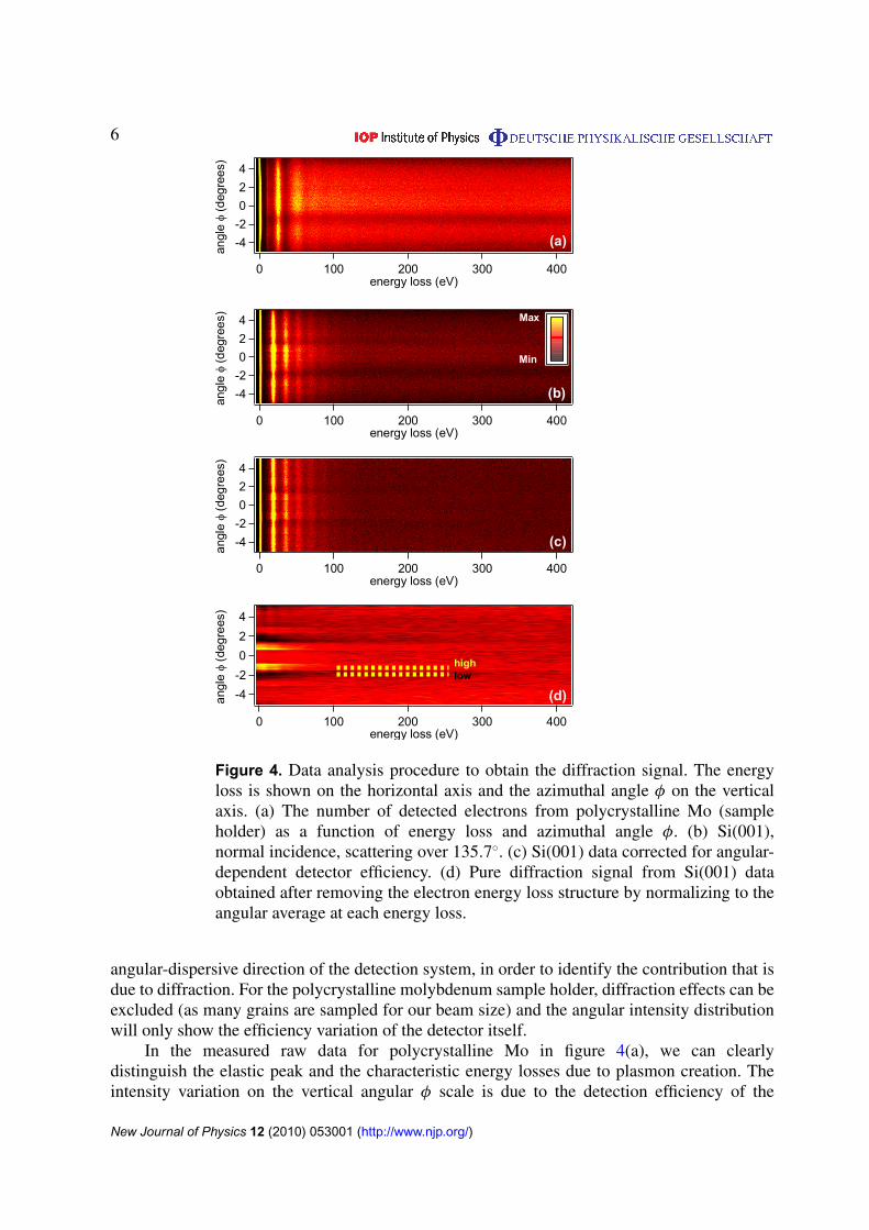
An example of spectra obtained with this spectrometer is given in figure 3 for ameasurement with the incoming beam aligned with the surface normal for two different angularranges of the analyzer. The sharp elastic peak is followed by a series of plasmon peaks. Surfaceplasmon intensities are weak for such energies and geometry. The spectra of the differentangular ranges of the spectrometer were normalized to equal intensity at the largest energyloss of this measurement (440 eV). Clearly the shape of the spectra is different, and the originof this difference will be investigated in detail in this paper.
3. Results
3.1. Data analysis
We measure the number of backscattered electrons as a function of energy and azimuthal angleφ. The raw data for energy losses of up to 400 eV are shown in figure 4(a) for polycrystallineMo and in figure 4(b) for Si(001). While the variations in detector efficiency along the energy-dispersive dimension of the position-sensitive detector are averaged out by scanning the ana-lyzer bias voltage [23], we still have to correct the spectra for efficiency variations along the
New Journal of Physics 12 (2010) 053001 (http://www.njp.org/)
5
φ
Gun A
Gun B
EnergyAnalyzer
Figure 2. Experimental geometry. The electron energy analyzer accepts scatteredelectrons on a cone of azimuthal directions φ corresponding to a fixed scatteringangle of θscat = 44.3 ◦ with respect to gun A and a scattering angle of 135.7◦ withrespect to the incident direction of electron gun B used in the present experiment.The angular acceptance of the energy analyzer in φ is ≈ ±5 ◦, with a resolutionof 1φ ≈ 0.1◦ (compare with figure 1).
0
2500
5000
7500
0 50 100 150
Energy Loss (eV)
×5
Cou
nts
−2.2° < φ < −1.6°
−1.4° < φ < −0.8°
Figure 3. Spectra measured with the incoming beam aligned with the surfacenormal. Spectra obtained for two different φ ranges of the analyzer have differentshapes.
New Journal of Physics 12 (2010) 053001 (http://www.njp.org/)
6
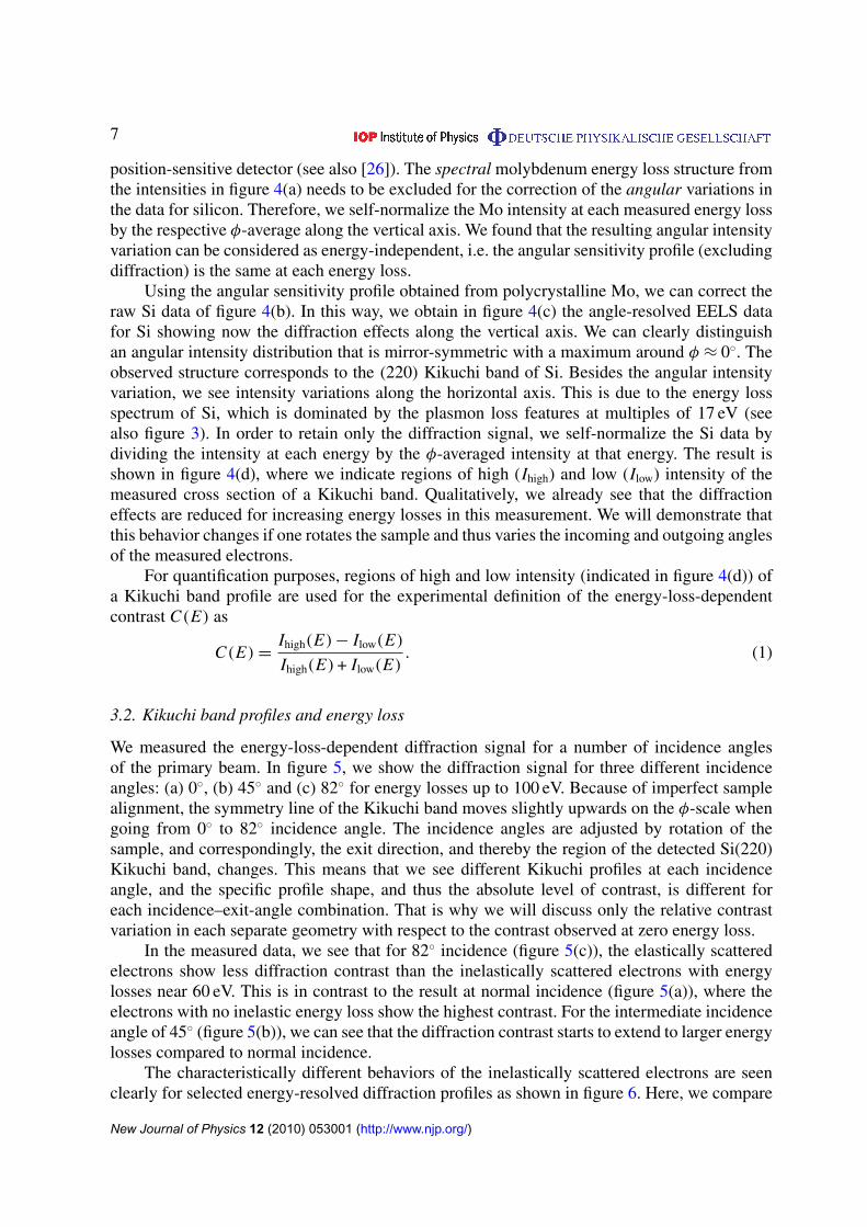
Figure 4. Data analysis procedure to obtain the diffraction signal. The energyloss is shown on the horizontal axis and the azimuthal angle φ on the verticalaxis. (a) The number of detected electrons from polycrystalline Mo (sampleholder) as a function of energy loss and azimuthal angle φ. (b) Si(001),normal incidence, scattering over 135.7◦. (c) Si(001) data corrected for angular-dependent detector efficiency. (d) Pure diffraction signal from Si(001) dataobtained after removing the electron energy loss structure by normalizing to theangular average at each energy loss.
angular-dispersive direction of the detection system, in order to identify the contribution that isdue to diffraction. For the polycrystalline molybdenum sample holder, diffraction effects can beexcluded (as many grains are sampled for our beam size) and the angular intensity distributionwill only show the efficiency variation of the detector itself.
In the measured raw data for polycrystalline Mo in figure 4(a), we can clearlydistinguish the elastic peak and the characteristic energy losses due to plasmon creation. Theintensity variation on the vertical angular φ scale is due to the detection efficiency of the
New Journal of Physics 12 (2010) 053001 (http://www.njp.org/)
7
position-sensitive detector (see also [26]). The spectral molybdenum energy loss structure fromthe intensities in figure 4(a) needs to be excluded for the correction of the angular variations inthe data for silicon. Therefore, we self-normalize the Mo intensity at each measured energy lossby the respective φ-average along the vertical axis. We found that the resulting angular intensityvariation can be considered as energy-independent, i.e. the angular sensitivity profile (excludingdiffraction) is the same at each energy loss.
Using the angular sensitivity profile obtained from polycrystalline Mo, we can correct theraw Si data of figure 4(b). In this way, we obtain in figure 4(c) the angle-resolved EELS datafor Si showing now the diffraction effects along the vertical axis. We can clearly distinguishan angular intensity distribution that is mirror-symmetric with a maximum around φ ≈ 0◦. Theobserved structure corresponds to the (220) Kikuchi band of Si. Besides the angular intensityvariation, we see intensity variations along the horizontal axis. This is due to the energy lossspectrum of Si, which is dominated by the plasmon loss features at multiples of 17 eV (seealso figure 3). In order to retain only the diffraction signal, we self-normalize the Si data bydividing the intensity at each energy by the φ-averaged intensity at that energy. The result isshown in figure 4(d), where we indicate regions of high (Ihigh) and low (Ilow) intensity of themeasured cross section of a Kikuchi band. Qualitatively, we already see that the diffractioneffects are reduced for increasing energy losses in this measurement. We will demonstrate thatthis behavior changes if one rotates the sample and thus varies the incoming and outgoing anglesof the measured electrons.
For quantification purposes, regions of high and low intensity (indicated in figure 4(d)) ofa Kikuchi band profile are used for the experimental definition of the energy-loss-dependentcontrast C(E) as
C(E) =Ihigh(E) − Ilow(E)
Ihigh(E) + Ilow(E). (1)
3.2. Kikuchi band profiles and energy loss
We measured the energy-loss-dependent diffraction signal for a number of incidence anglesof the primary beam. In figure 5, we show the diffraction signal for three different incidenceangles: (a) 0◦, (b) 45◦ and (c) 82◦ for energy losses up to 100 eV. Because of imperfect samplealignment, the symmetry line of the Kikuchi band moves slightly upwards on the φ-scale whengoing from 0◦ to 82◦ incidence angle. The incidence angles are adjusted by rotation of thesample, and correspondingly, the exit direction, and thereby the region of the detected Si(220)Kikuchi band, changes. This means that we see different Kikuchi profiles at each incidenceangle, and the specific profile shape, and thus the absolute level of contrast, is different foreach incidence–exit-angle combination. That is why we will discuss only the relative contrastvariation in each separate geometry with respect to the contrast observed at zero energy loss.
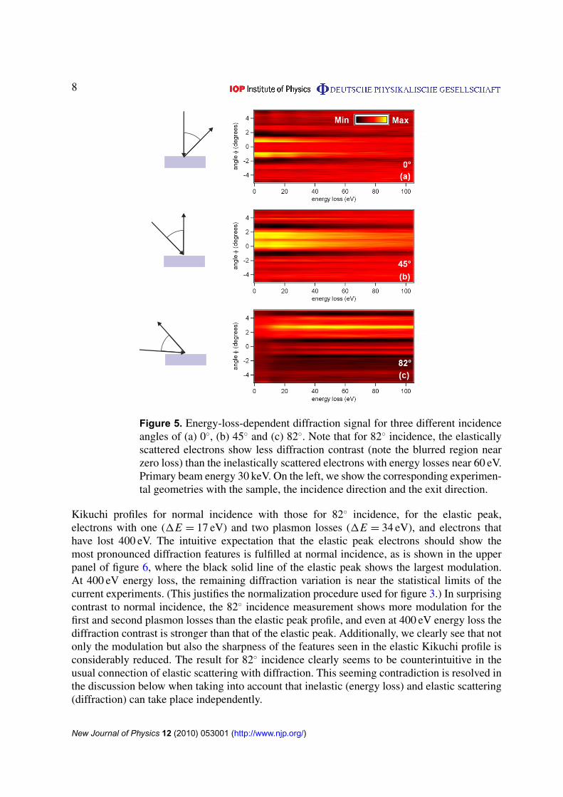
In the measured data, we see that for 82◦ incidence (figure 5(c)), the elastically scatteredelectrons show less diffraction contrast than the inelastically scattered electrons with energylosses near 60 eV. This is in contrast to the result at normal incidence (figure 5(a)), where theelectrons with no inelastic energy loss show the highest contrast. For the intermediate incidenceangle of 45◦ (figure 5(b)), we can see that the diffraction contrast starts to extend to larger energylosses compared to normal incidence.
The characteristically different behaviors of the inelastically scattered electrons are seenclearly for selected energy-resolved diffraction profiles as shown in figure 6. Here, we compare
New Journal of Physics 12 (2010) 053001 (http://www.njp.org/)
8
Figure 5. Energy-loss-dependent diffraction signal for three different incidenceangles of (a) 0◦, (b) 45◦ and (c) 82◦. Note that for 82◦ incidence, the elasticallyscattered electrons show less diffraction contrast (note the blurred region nearzero loss) than the inelastically scattered electrons with energy losses near 60 eV.Primary beam energy 30 keV. On the left, we show the corresponding experimen-tal geometries with the sample, the incidence direction and the exit direction.
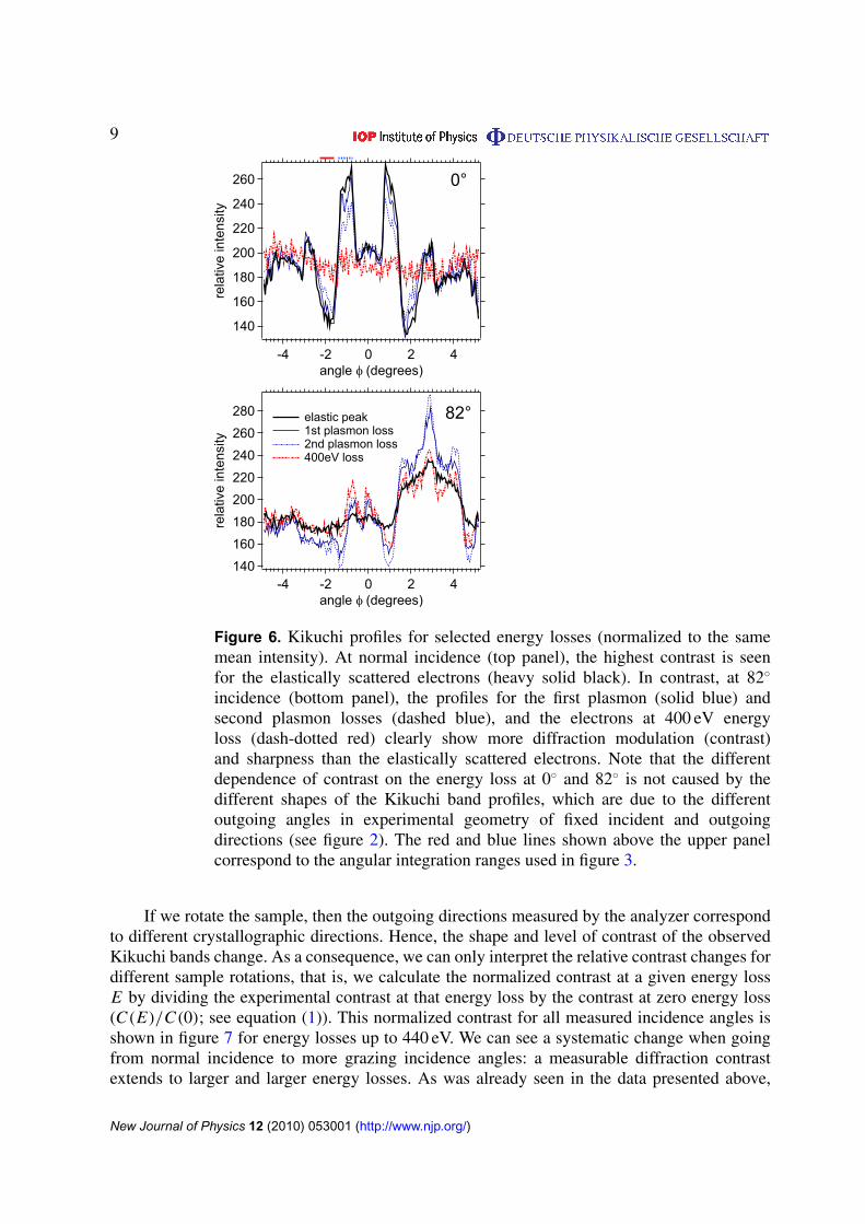
Kikuchi profiles for normal incidence with those for 82◦ incidence, for the elastic peak,electrons with one (1E = 17 eV) and two plasmon losses (1E = 34 eV), and electrons thathave lost 400 eV. The intuitive expectation that the elastic peak electrons should show themost pronounced diffraction features is fulfilled at normal incidence, as is shown in the upperpanel of figure 6, where the black solid line of the elastic peak shows the largest modulation.At 400 eV energy loss, the remaining diffraction variation is near the statistical limits of thecurrent experiments. (This justifies the normalization procedure used for figure 3.) In surprisingcontrast to normal incidence, the 82◦ incidence measurement shows more modulation for thefirst and second plasmon losses than the elastic peak profile, and even at 400 eV energy loss thediffraction contrast is stronger than that of the elastic peak. Additionally, we clearly see that notonly the modulation but also the sharpness of the features seen in the elastic Kikuchi profile isconsiderably reduced. The result for 82◦ incidence clearly seems to be counterintuitive in theusual connection of elastic scattering with diffraction. This seeming contradiction is resolved inthe discussion below when taking into account that inelastic (energy loss) and elastic scattering(diffraction) can take place independently.
New Journal of Physics 12 (2010) 053001 (http://www.njp.org/)
9
Figure 6. Kikuchi profiles for selected energy losses (normalized to the samemean intensity). At normal incidence (top panel), the highest contrast is seenfor the elastically scattered electrons (heavy solid black). In contrast, at 82◦
incidence (bottom panel), the profiles for the first plasmon (solid blue) andsecond plasmon losses (dashed blue), and the electrons at 400 eV energyloss (dash-dotted red) clearly show more diffraction modulation (contrast)and sharpness than the elastically scattered electrons. Note that the differentdependence of contrast on the energy loss at 0◦ and 82◦ is not caused by thedifferent shapes of the Kikuchi band profiles, which are due to the differentoutgoing angles in experimental geometry of fixed incident and outgoingdirections (see figure 2). The red and blue lines shown above the upper panelcorrespond to the angular integration ranges used in figure 3.
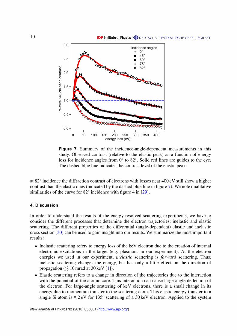
If we rotate the sample, then the outgoing directions measured by the analyzer correspondto different crystallographic directions. Hence, the shape and level of contrast of the observedKikuchi bands change. As a consequence, we can only interpret the relative contrast changes fordifferent sample rotations, that is, we calculate the normalized contrast at a given energy lossE by dividing the experimental contrast at that energy loss by the contrast at zero energy loss(C(E)/C(0); see equation (1)). This normalized contrast for all measured incidence angles isshown in figure 7 for energy losses up to 440 eV. We can see a systematic change when goingfrom normal incidence to more grazing incidence angles: a measurable diffraction contrastextends to larger and larger energy losses. As was already seen in the data presented above,
New Journal of Physics 12 (2010) 053001 (http://www.njp.org/)
10
Figure 7. Summary of the incidence-angle-dependent measurements in thisstudy. Observed contrast (relative to the elastic peak) as a function of energyloss for incidence angles from 0◦ to 82◦. Solid red lines are guides to the eye.The dashed blue line indicates the contrast level of the elastic peak.
at 82◦ incidence the diffraction contrast of electrons with losses near 400 eV still show a highercontrast than the elastic ones (indicated by the dashed blue line in figure 7). We note qualitativesimilarities of the curve for 82◦ incidence with figure 4 in [29].
4. Discussion
In order to understand the results of the energy-resolved scattering experiments, we have toconsider the different processes that determine the electron trajectories: inelastic and elasticscattering. The different properties of the differential (angle-dependent) elastic and inelasticcross section [30] can be used to gain insight into our results. We summarize the most importantresults:
• Inelastic scattering refers to energy loss of the keV electron due to the creation of internalelectronic excitations in the target (e.g. plasmons in our experiment). At the electronenergies we used in our experiment, inelastic scattering is forward scattering. Thus,inelastic scattering changes the energy, but has only a little effect on the direction ofpropagation (. 10 mrad at 30 keV [1]).
• Elastic scattering refers to a change in direction of the trajectories due to the interactionwith the potential of the atomic core. This interaction can cause large-angle deflection ofthe electron. For large-angle scattering of keV electrons, there is a small change in itsenergy due to momentum transfer to the scattering atom. This elastic energy transfer to asingle Si atom is ≈2 eV for 135◦ scattering of a 30 keV electron. Applied to the system
New Journal of Physics 12 (2010) 053001 (http://www.njp.org/)
11
of the ‘incident electron’ and the macroscopic ‘backscattering crystal’ as the scatteringpartners (instead of ‘incident electron’ and microscopic ‘scattering atom’), this meansthat 2 eV are finally transferred to internal degrees of freedom (phonons) in the sample.In this macroscopic picture, the more accurate description of the backscattering eventsas sources for the Kikuchi pattern would be ‘quasi-elastic’ or ‘thermal diffuse’. Thefundamental microscopic interaction is, however, elastic scattering at the atomic cores withthe concomitant recoil energy transfer.
Concerning the coherence of the electron waves in the various scattering processes, wenote that large-angle scattering of keV electrons is mostly incoherent with respect to theincident electron wave as the available recoil energy for an atom is much larger than typicalphonon energies of the crystal under observation [28]. For the detection of an electron in ourbackscattering experiment, at least one large-angle scattering event is a prerequisite. This iswhere the coherence to the incident beam will be lost. Small-angle scattering elastic scatteringevents occur as well, even much more frequently, as the cross section for forward elasticscattering is much larger. Forward elastic scattering involves much smaller momentum transfers(smaller recoil energy) compared to a backscattering event and thus the scattered waves canstay coherent with respect to each other to a larger degree. This is the basis for the observeddiffraction effects of the incoming and outgoing electron waves.
We summarize these results into the following relations, which we assume to be valid underour experimental conditions:
interaction with target electrons → large energy loss and small change in directionstrong interaction with atomic cores → recoil loss and large change in directionweak interaction with atomic cores → no energy loss and coherent forward scattering
In this scheme, inelastic scattering and large-angle elastic scattering lead effectively to a loss ofthe phase information of the scattered electron waves with respect to the electron wave beforethe scattering event. After the phase information is lost, the scattered electron waves can stillinteract with the crystal individually. The ‘new’ electron waves created by incoherent elasticbackscattering all appear to emanate from atomic sites. As a consequence, their individualinterference patterns with the crystal show the structures in the form of the Kikuchi patterns.In contrast, those ‘new’ electron waves that are created by inelastic plasmon scattering aremore isotropically distributed over the unit cell, not just at the lattice atomic sites. Hence, theirdiffraction effects will tend to average out [31].
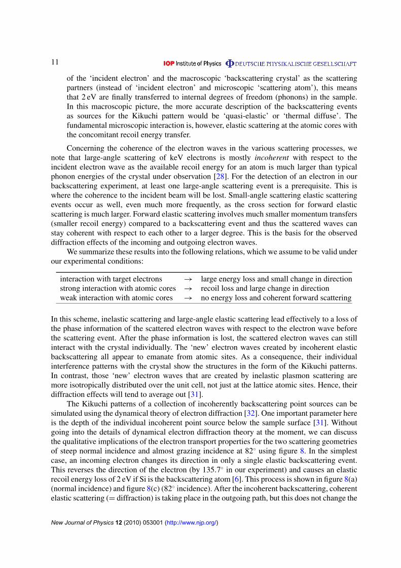
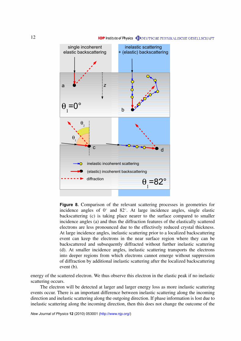
The Kikuchi patterns of a collection of incoherently backscattering point sources can besimulated using the dynamical theory of electron diffraction [32]. One important parameter hereis the depth of the individual incoherent point source below the sample surface [31]. Withoutgoing into the details of dynamical electron diffraction theory at the moment, we can discussthe qualitative implications of the electron transport properties for the two scattering geometriesof steep normal incidence and almost grazing incidence at 82◦ using figure 8. In the simplestcase, an incoming electron changes its direction in only a single elastic backscattering event.This reverses the direction of the electron (by 135.7◦ in our experiment) and causes an elasticrecoil energy loss of 2 eV if Si is the backscattering atom [6]. This process is shown in figure 8(a)(normal incidence) and figure 8(c) (82◦ incidence). After the incoherent backscattering, coherentelastic scattering (= diffraction) is taking place in the outgoing path, but this does not change the
New Journal of Physics 12 (2010) 053001 (http://www.njp.org/)
12
θ1
a
θ1
θ2
θ1
Figure 8. Comparison of the relevant scattering processes in geometries forincidence angles of 0◦ and 82◦. At large incidence angles, single elasticbackscattering (c) is taking place nearer to the surface compared to smallerincidence angles (a) and thus the diffraction features of the elastically scatteredelectrons are less pronounced due to the effectively reduced crystal thickness.At large incidence angles, inelastic scattering prior to a localized backscatteringevent can keep the electrons in the near surface region where they can bebackscattered and subsequently diffracted without further inelastic scattering(d). At smaller incidence angles, inelastic scattering transports the electronsinto deeper regions from which electrons cannot emerge without suppressionof diffraction by additional inelastic scattering after the localized backscatteringevent (b).
energy of the scattered electron. We thus observe this electron in the elastic peak if no inelasticscattering occurs.
The electron will be detected at larger and larger energy loss as more inelastic scatteringevents occur. There is an important difference between inelastic scattering along the incomingdirection and inelastic scattering along the outgoing direction. If phase information is lost due toinelastic scattering along the incoming direction, then this does not change the outcome of the
New Journal of Physics 12 (2010) 053001 (http://www.njp.org/)
13
experiment, as phase information is lost anyway in the subsequent large-angle elastic scatteringevent. Loss of phase information due to inelastic scattering along the outgoing trajectory doesaffect the outcome of the experiments as these process is will reduce the contrast in the Kikuchipatterns.
In the two geometries, however, the ratios of the lengths of the incoming and outgoingtrajectories are different. For normal incidence, the incoming trajectory is cos 0◦/cos 44.3◦
≈
1.4 times shorter than the outgoing trajectory, whereas in the tilted geometry it is cos (82◦−
44.3◦)/cos (82◦) ≈ 5.7 times longer than the outgoing trajectory. This has severe implicationsin terms of the dynamical electron diffraction process. For the electrons observed in theelastic peak, the total path length (incoming plus outgoing) without inelastic scattering will beultimately limited by the inelastic mean free path (≈ 40 nm for 30 keV e− in Si [33, 34]). Due tothe geometry at 82◦ incidence, the ingoing and outgoing parts of the shortest trajectories will bedistributed roughly as 6:1. Considering the inelastic mean free path of 40 nm as characteristic,we obtain a distribution of 36 nm : 6 nm between the ingoing and outgoing path lengths. Weknow from dynamical diffraction theory that if the crystal thickness (the outgoing path lengthin our case) is below a quarter of the extinction distance [35] of the relevant reflection, theresulting Kikuchi diffraction features will be reduced in sharpness and contrast [31]. Insimplified terms: if the crystal is too thin, then diffraction cannot be strong. For the (220)
reflection in Si at 30 kV, the extinction distance is ≈46 nm (as calculated in the simulationsbelow) and thus the length of the outgoing trajectories is well below a quarter of this value forthe elastic peak of Si at the 82◦ measurement. This explains the observation of the reducedsharpness and lower contrast for the Kikuchi band profiles of the elastic peak in figure 6:these electrons at 82◦ originate from a depth that is too low for sharp diffraction patterns. Inthis respect, we are highly surface-sensitive when measuring the group of electrons shown infigure 8(c), although this comes at the price of less pronounced diffraction. Similar observationshave been made using energy-filtered EBSD by Deal et al [29]. Trajectories with one inelasticevent allowed have on average a length of two inelastic mean free paths. Thus, for the firstand second plasmon features, the outgoing trajectories are also correspondingly longer, and thediffraction effects are better developed at 82◦ incidence.
In figures 8(c) and (d), we see how plasmon losses before backscattering can move theincoherent point source deeper into the crystal at grazing incidence without increasing theoutgoing path length to a value where inelastic scattering (reduction in contrast) becomes im-portant. This increased depth implies a larger crystal region above the source and results in thefuller development of dynamical diffraction effects. In this way, the sharper Kikuchi band pro-files and higher contrast for the one and two plasmon loss features shown in figure 6 are caused.
With an increase in the number of plasmon losses, the backscattering depth reaches avalue where inelastic losses in the outgoing path become important. This is more pronouncedat 0◦ incidence, where the inelastic events are distributed more evenly over the outgoing andincoming trajectories, due to the geometric ratio of 1.4 : 1 as estimated above. Here, the effectof longer outgoing path length (sharper diffraction) is less important than the loss of electronsdue to inelastic scattering events (less diffraction contrast), because already the electrons in theelastic peak are backscattered from deeper within the crystal (see below). In general, for energylosses larger than about 50 eV (corresponding to the creation of three plasmons or more in ourexperiments), the effect of more inelastic scattering along the outgoing trajectories is having astrong effect and that is why the contrast decreases for all geometries at larger energy losses(see figure 7).
New Journal of Physics 12 (2010) 053001 (http://www.njp.org/)
14
In order to estimate the influence of the depth distribution of the incoherent Kikuchipattern sources more quantitatively, we develop some simple model approximations, thatwill be the basis for dynamical diffraction simulations discussed afterwards. Based on thearguments in [36], we assume that elastic backscattering takes place in processes withV-type trajectories [37], which are dominated by a single large-angle scattering event, withadditional scattering events on the incoming and outgoing paths. We will assume that thelarge-angle scattering events will create the incoherent sources, while the additional elasticscattering with the crystal in the outgoing path actually forms their Kikuchi patterns. We thususe the statistical Monte Carlo ‘particle’ picture to derive a simple average depth distribution ofthe incoherent large-angle scattering sources, which is then used as input for the subsequentquantum-mechanical treatment of diffraction in the ‘wave’ picture. This is a considerablesimplification but leads to consistent results in the interpretation of our experiments, as wewill show below.
The probability of N scattering events is assumed to be distributed according to a Poissonstatistical process with mean free path λ and path length s:
W i/eN (s) = (s/λi/e)
N e−(s/λi/e)
N !. (2)
The simplest model case would be a depth distribution ρnine
(z) given by single elastic inco-herent backscattering ne = 1 distributed according to the process W e
1 (s) with elastic mean freepath λe under the condition of ni = 0 inelastic events W i
0(s) with inelastic mean free path λi.At the incidence angle θ1 (see figure 8), the relative probability for backscattering at depth z isgiven by
ρ01(z) = W i
0(z/ cos θ1)W e1 (z/ cos θ1). (3)
In order to see the influence of inelastic forward scattering events on the depth distribution,we allow up to ni = 2 additional inelastic events on the incoming path:
ρ0,1,21 (z) = W i
0,1,2(z/ cos θ1)W e1 (z/ cos θ1). (4)
We note here that the depth distribution ρnine
(z) gives the number of backscattered electronsthat starts from an incoherent point source at depth z below the surface. Inelastic scatteringin the outgoing diffraction phase will additionally attenuate the intensity from the consideredprocesses according to the outgoing path length by a factor of W i
0(z/cos θ2). This outgoingattenuation is treated by an imaginary part of the scattering potential in the dynamical diffractionsimulation.
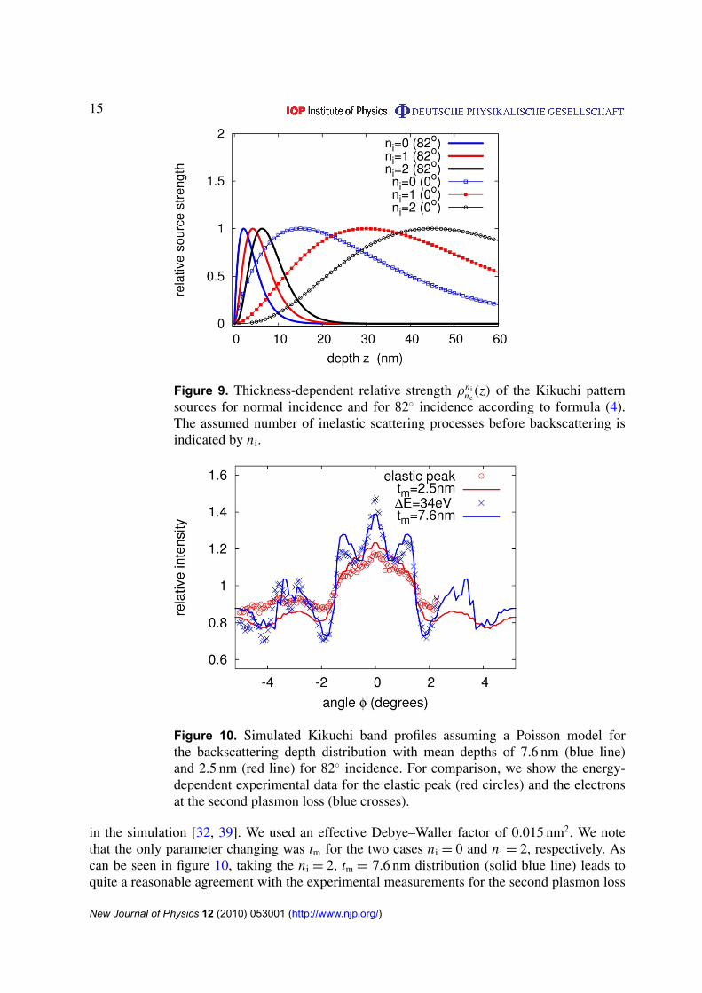
In figure 9, we show the normalized depth distributions for the two incidence angles ofθ1 = 0◦ and θ1 = 82◦ calculated according to equation (4). For the elastic and inelastic mean freepaths, we took the values of λi = 40 nm [33, 34] and λe = 24 nm [38] for Si at 30 keV. We canclearly see the increased surface sensitivity at shallow incidence compared to normal incidence.At 82◦ incidence, the single elastic scattering depth distributions for ni = 0 and ni = 2 can beapproximated by an effective Poisson model with mean depth tm:ρ(z) ∝ (z/tm) × exp(−z/tm).Including the geometric depth enhancement factor of 1/cos 37.7◦
= 1.3 due to the outgoingangle θ2, we obtain tm = 2.5 nm for ni = 0 and tm = 7.6 nm for ni = 2.
Using these depth-dependent model distributions, we carried out dynamical simulationsfor silicon at 30 keV in order to show the correlation between the shape of the observedKikuchi band profiles and the mean depth of backscattering in the measurements for 82◦
incidence. About 1000 reflections with minimum lattice spacing of 0.04 nm were included
New Journal of Physics 12 (2010) 053001 (http://www.njp.org/)
15
Figure 9. Thickness-dependent relative strength ρnine
(z) of the Kikuchi patternsources for normal incidence and for 82◦ incidence according to formula (4).The assumed number of inelastic scattering processes before backscattering isindicated by ni.
Figure 10. Simulated Kikuchi band profiles assuming a Poisson model forthe backscattering depth distribution with mean depths of 7.6 nm (blue line)and 2.5 nm (red line) for 82◦ incidence. For comparison, we show the energy-dependent experimental data for the elastic peak (red circles) and the electronsat the second plasmon loss (blue crosses).
in the simulation [32, 39]. We used an effective Debye–Waller factor of 0.015 nm2. We notethat the only parameter changing was tm for the two cases ni = 0 and ni = 2, respectively. Ascan be seen in figure 10, taking the ni = 2, tm = 7.6 nm distribution (solid blue line) leads toquite a reasonable agreement with the experimental measurements for the second plasmon loss
New Journal of Physics 12 (2010) 053001 (http://www.njp.org/)
16
(1E = 34 eV). When the mean depth is reduced to tm = 2.5 nm (solid red line), we see that thetwo peaks on the edge of the central Kikuchi band are disappearing. This is in agreement withthe expectation that the elastic peak is sensitive to a thinner surface region than the electrons thathave experienced plasmon losses and thus on average come from deeper regions. In agreementwith the experimental data, the sharpness of the measured features is clearly reduced in thesimulations for tm = 2.5 nm. Due to our simple assumptions about the depth profile of theincoherent sources, we do not expect quantitative agreement of measurements and simulations.Nevertheless, the agreement with the experiments is good.
Already the simple model that we used above shows that via the measurement of energy-resolved diffraction profiles, we can gain access to depth-dependent transport of the elasticallyand inelastically scattered electrons. In this way, electron energy loss measurements can actuallybenefit from diffraction effects. We expect that, in a next step, the application of MonteCarlo simulations can give more realistic depth distributions of the incoherently backscatteredelectrons as a function of their energy loss. Ultimately, a quantitative simulation needs also toinclude diffraction of the incoming electron waves. The corresponding effects of the incomingbeam have been neglected in the current analysis, since the numbers of backscattered electronsfor different incidence angles have not been normalized with respect to each other. It should bepossible, however, to account for these effects in future experiments.
5. Summary
Our investigations give quantitative insights into the details of EBSD pattern formation as afunction of energy loss and should help us to analyze the possible limits of the current techniqueand the future possibilities of EBSD, potentially in energy-resolved modes [29]. Apart from thepractical application in EBSD, our angle-resolved REELS measurements also provide referencedata for quantitative theories of energy-resolved inelastic electron (back)scattering [40]–[44],which is one of the most general and difficult problems in electron diffraction theory.
As REELS measurements provide unique access to important properties of solid-statesystems like the dielectric function [45, 46], a quantification of the influence of diffraction onthese measurements is also necessary. Furthermore, electron momentum spectroscopy (EMS)of crystalline systems will benefit from a better understanding of diffraction effects [47, 48].Since the Kikuchi pattern formation process in EBSD shares many common features withphotoelectron diffraction, we can also expect that the presented measurements will be relevantfor the interpretation of hard x-ray photoelectron diffraction (HXPD) experiments [49].The ultimate combination of SEM technology with high-resolution electron energy lossspectroscopy and angle-resolved diffraction capability can be expected to provide improvedpossibilities of fundamental materials analysis. As a further application of high-resolutionREELS experiments, we mention the proposal to achieve a time resolution of tens offemtoseconds via energy-resolved detection of diffracted intensities from chirped electronpulses that are initially excited by an ultrashort laser from a photocathode [50].
Acknowledgments
This work was made possible by a grant from the Australian Research Council. We thankLes Allen for stimulating discussions and the Atomic and Molecular Physics Laboratories atANU for technical support.
New Journal of Physics 12 (2010) 053001 (http://www.njp.org/)
17
References
[1] Egerton R F 2009 Electron energy-loss spectroscopy in the TEM Rep. Progr. Phys. 72 016502[2] Egerton R F 1996 Electron Energy-Loss Spectroscopy in the Electron Microscope 2nd edn (Berlin: Springer)[3] Schattschneider P 1986 Fundamentals of Inelastic Electron Scattering (Berlin: Springer)[4] Wang Z L 1996 Reflection Electron Microscopy and Spectroscopy for Surface Analysis (Cambridge:
Cambridge University Press)[5] Boersch H, Wolter R and Schoenebeck H 1967 Elastische Energieverluste kristallgestreuter Elektronen
Z. Phys. A 199 124–34[6] Went M R and Vos M 2008 Rutherford backscattering using electrons as projectiles: underlying principles
and possible applications Nucl. Instrum. Methods Phys. Res. B 266 998–1011[7] Powell C J and Swan J B 1959 Origin of the characteristic electron energy losses in aluminum Phys. Rev. 115
869–75[8] Schilling J 1976 Energieverlustmessungen von schnellen Elektronen an Oberflächen von Ga, In, Al und Si
Z. Phys. B 25 61–7[9] Jablonski A 2005 Modeling of elastic and inelastic electron backscattering from surfaces Prog. Surf. Sci. 79
3–27[10] Werner W S M 2009 Electron transport for spectrum analysis and experiment design J. Electron Spectrosc.
Relat. Phenom. at press, doi:10.1016/j.elspec.2009.09.004[11] Ichimiya A and Cohen P I 2004 Reflection High-Energy Electron Diffraction (Cambridge: Cambridge
University Press)[12] Kikuchi S 1928 Diffraction of cathode rays by mica Proc. Imper. Acad. Japan 4 354–6,
http:/ /www.journalarchive.jst.go.jp/jnlpdf.php?cdjournal=pjab1912&cdvol=4&noissue=7&startpage=354&lang=en&from=jnlabstract
[13] Alam M N, Blackman M and Pashley D W 1954 High-angle Kikuchi patterns Proc. R. Soc. A 221 224–42,http://www.jstor.org/stable/100898
[14] Schwartz A J, Kumar M, Adams B L and Field D P (ed) 2009 Electron Backscatter Diffraction in MaterialsScience 2nd edn (Berlin: Springer)
[15] Wilkinson A J and Hirsch P B 1997 Electron diffraction based techniques in scanning electron microscopy ofbulk materials Micron 28 279–308
[16] Schwarzer R A 1997 Automated crystal lattice orientation mapping using a computer-controlled SEM Micron28 249–65
[17] Dingley D 2004 Progressive steps in the development of electron backscatter diffraction and orientationimaging microscopy J. Microsc. 213 214–24
[18] Randle V 2008 Recent developments in electron backscatter diffraction Adv. Imaging Electron Phys. 151363–416
[19] Joy D C, Newbury D E and Davidson D L 1982 Electron channeling patterns in the scanning electronmicroscope J. Appl. Phys. 53 R81–122
[20] Krivanek O L, Tanishiro Y, Takayanagi K and Yagi K 1983 Electron energy loss spectroscopy in glancingreflection from bulk crystals Ultramicroscopy 11 215–22
[21] Horio Y, Hashimoto Y and Ichimiya A 1996 A new type of RHEED apparatus equipped with an energy filterAppl. Surf. Sci. 100–101 292–6
[22] Nakahara H, Hishida T and Ichimiya A 2003 Inelastic electron analysis in reflection high-energy electrondiffraction condition Appl. Surf. Sci. 212–213 157–61
[23] Vos M, Cornish G P and Weigold E 2000 High-energy (e, 2e) spectrometer for the study of the spectralmomentum density of materials Rev. Sci. Instrum. 71 3831–40
[24] Vos M 2001 Observing atom motion by electron-atom compton scattering Phys. Rev. A 65 012703[25] Vos M and Went M R 2008 Splitting the plasmon peak in high-energy reflection electron energy loss
experiments J. Electron Spectrosc. Relat. Phenom. 162 1–7
New Journal of Physics 12 (2010) 053001 (http://www.njp.org/)
18
[26] Went M, Winkelmann A and Vos M 2009 Quantitative measurements of backscattered electron diffractionpatterns using an electrostatic analyzer Ultramicroscopy 109 1211
[27] Vos M, Aizel K and Winkelmann A 2010 Experimental observation of the strong influence of crystal orien-tation on electron Rutherford backscattering spectra Surf. Sci. at press, doi:10.1016/j.susc.2010.02.016
[28] Lipkin H J 1973 Quantum Mechanics: New Approaches to Selected Topics (Amsterdam: North-Holland)[29] Deal A, Hooghan T and Eades A 2008 Energy-filtered electron backscatter diffraction Ultramicroscopy 108
116–25[30] Werner W S M 2001 Electron transport in solids for quantitative surface analysis Surf. Int. Anal. 31 141–76[31] Winkelmann A 2009 Principles of depth-resolved Kikuchi pattern simulation for electron backscatter
diffraction J. Microsc. at press[32] Winkelmann A 2009 Dynamical simulation of electron backscatter diffraction patterns Electron Backscatter
Diffraction in Materials Science ed A J Schwartz, M Kumar, B L Adams and D P Field (Berlin: Springer)chapter 2, http://www.springer.com/cda/content/document/cda downloaddocument/9780387881355-c2.pdf?SGWID=0-0-45-749108-p173906909
[33] Tanuma S, Powell C J and Penn D R 1993 Calculations of electron inelastic mean free paths. V. Data for 14organic compounds over the 50–2000 eV range Surf. Interface Anal. 21 165
[34] Powell C J and Jablonski A 1999 Evaluation of calculated and measured electron inelastic mean free pathsnear solid surfaces J. Phys. Chem. Refer. Data 28 197–62
[35] De Graef M 2003 Introduction to Conventional Transmission Electron Microscopy (Cambridge: CambridgeUniversity Press)
[36] Werner W S M 2005 Trajectory reversal approach for electron backscattering from solid surfaces Phys. Rev.B 71 115415
[37] Yubero F, Pauly N, Dubus A and Tougaard S 2008 Test of validity of the V-type approach for electrontrajectories in reflection electron energy loss spectroscopy Phys. Rev. B 77 245405
[38] Browning R, Li T Z, Chui B, Jun Ye, Pease R F W, Czyzewski Z and Joy D C 1994 Empirical forms for theelectron/atom elastic scattering cross sections from 0.1 to 30 keV J. Appl. Phys. 76 2016–22
[39] Winkelmann A, Trager-Cowan C, Sweeney F, Day A P and Parbrook P 2007 Many-beam dynamicalsimulation of electron backscatter diffraction patterns Ultramicroscopy 107 414–21
[40] Dudarev S L, Peng L M and Whelan M J 1993 Correlations in space and time and dynamical diffraction ofhigh-energy electrons by crystals Phys. Rev. B 48 13408
[41] Dudarev S L, Rez P and Whelan M J 1995 Theory of electron backscattering from crystals Phys. Rev. B51 3397
[42] Schattschneider P, Nelhiebel M, Souchay M and Jouffrey B 2000 The physical significance of the mixeddynamic form factor Micron 31 333–45
[43] Schattschneider P, Jouffrey B and Nelhiebel M 1996 Dynamical diffraction in electron-energy-lossspectrometry: the independent bloch wave model Phys. Rev. B 54 3861–8
[44] Schattschneider P and Jouffrey B 2003 Channeling, localization and the density matrix in inelastic electronscattering Ultramicroscopy 96 453–62
[45] Went M R, Vos M and Werner W S M 2008 Extracting the Ag surface and volume loss functions fromreflection electron energy loss spectra Surf. Sci. 602 2069–77
[46] Werner W S M, Went M R, Vos M, Glantschnig K and Ambrosch-Draxl C 2008 Measurement and densityfunctional calculations of optical constants of Ag and Au from infrared to vacuum ultraviolet wavelengthsPhys. Rev. B 77 161404
[47] Fang Z, Matthews R S, Utteridge S, Vos M, Canney S A, Guo X, McCarthy I E and Weigold E 1998 Electron-momentum spectroscopy of crystal silicon Phys. Rev. B 57 12882–9
[48] Vos M, Kheifets A S, Bowles C, Chen C, Weigold E and Aryasetiawan F 2004 Electronic structure of copperstudied by electron momentum spectroscopy Phys. Rev. B 70 205111
[49] Winkelmann A, Fadley C S and Garcia de Abajo F J 2008 High-energy photoelectron diffraction: modelcalculations and future possibilities New. J. Phys. 10 113002
[50] Baum P and Zewail A 2008 Femtosecond diffraction with chirped electron pulses Chem. Phys. Lett. 462 14–7
New Journal of Physics 12 (2010) 053001 (http://www.njp.org/)