electrical and microwave characteristics of silver ... · electrical and microwave characteristics...
TRANSCRIPT

Electrical and microwave characteristics of silvernanoparticle composites
Research on non-lineair DC and RF reflection and transmission behaviour
Rik Groenen
University of TwenteEnschede, May 2010

Electrical and microwave characteristics of silvernanoparticle composites
Research on non-lineair DC and RF reflection and transmission behaviour
A Thesis Submitted to the Faculty of Science and Technology at the University of Twente, inPartial Fulfillment of the Requirements for the Degree of Master of Science
Rik GroenenMay 2010
Graduation committee:
Prof. dr. ing. D.H.A. BlankProf. dr. ing. G. RijndersProf. dr. ir. J.W.M. HilgenkampDr. ir. S.M. van den Berg
Inorganic Material Science (IMS)Faculty of Science and TechnologyMESA+ Institute of NanotechnologyUniversity of TwenteThe NetherlandsThales Nederland BV
Cover: TEM images of clusters of silver nanoparticles. Particles are about 50-100nm in size.

Abstract
Research has been carried out on the electrical and microwave characterization of silvernanoparticles composite material. Main focus has been the investigation of the presenceof non linear resistive and reflective behaviour. This behaviour is most likely to occur incomposites with a filler ratio near the percolation threshold. Therefore, research focusseson fabrication and characterization of composite material in which silver nanoparticles areused, coated with an insulating shell.
Electrical characterization has shown non linear resistive behaviour for composite materialwith a filler ratio well above the percolation threshold. This verifies the functionality of aninsulating coating, were a composite material which is relatively easy to fabricate will showremarkable non linear resistive behaviour. The increase in conductivity with increasingapplied voltage strongly indicates a tunneling mechanism between particles.
Microwave response measurements showed a transition in the composite material at around20% filler ratio up to were the composite theoretically can be described as a dielectric.Reversible power dependent reflectivity has not been observed, though for high powermicrowaves the composite showed an irreversible alteration in reflective response. Fur-thermore, due to a layered structure with different loss, significant asymmetrical reflectiveresponse is observed.
v

vi
Preface
After my internship at Stanford University, California, USA, I started in April 2008 withthe final stage of the master program Applied Physics, my graduation project. After aperiod of orientation, I was offered the possibility to carry out research in collaborationwith Thales BV. For me this was a great opportunity. Where my internship was mainly agreat personal experience, it lacked an inspirational scientific experience. The idea of thecollaboration between physics with a potential commercial application appealed to me.What we didn’t know, was the wideness of the field of research we entered in our firstmeetings. It took quite some time to determine the actual focus of the research, whichfinally has resulted in a report which makes first steps towards more extensive research onthe investigated materials, which have great potential in showing interesting behaviour.Overall, this period of graduation was a very learningful experience where I rediscoveredmy fascination for physics and research.
First, I would like to thank Guus Rijnders en Simon van den Berg for the fruitful discus-sions we had in this field, where we could not only rely on knowledge in research fieldsfamiliar to us, but where we were challenged to take leaps into the unknown. Where atfirst it was a challenge for me to stay motivated in this process, I learned to appreciate this,the beauty of research in its purest form. Also always relaxing were our discussions aboutmusic and guitars, for me as a musician the confirmation that, although seemingly contra-dictory, the creative side of music and the abstract side in physics complement eachothertremendously.
Next, I would like to thank de BRAK and Heerendispuut Bracque for its beautiful friend-ships, inspirational discussions about all facets in life, the wednesday evenings and thefun weekends. Furthermore, my band, Duck4Cover, the musical inspiration it brings meand all the amazing adventures we had on the road. Then of course, my roommates fromStudentenpaleis de Handige Jongens, with whom I lived together for six years. I wouldlike to thank my parents, my brother and his wife for their loving support and Nadya forher love and care!
R.G.
vii

viii
Contents
Abstract v
Preface vii
1 Introduction 1
2 Theoretical background and research questions 52.1 Percolation theory . . . . . . . . . . . . . . . . . . . . . . . . . . . . . . . . 52.2 Field dependent conductance . . . . . . . . . . . . . . . . . . . . . . . . . . 62.3 Microwave response materials . . . . . . . . . . . . . . . . . . . . . . . . . . 82.4 Research goals . . . . . . . . . . . . . . . . . . . . . . . . . . . . . . . . . . 11
3 Structural characterization 133.1 Silver nanoparticles . . . . . . . . . . . . . . . . . . . . . . . . . . . . . . . . 13
3.1.1 TEM characterization . . . . . . . . . . . . . . . . . . . . . . . . . . 143.1.2 SEM characterization . . . . . . . . . . . . . . . . . . . . . . . . . . 153.1.3 XPS characterization . . . . . . . . . . . . . . . . . . . . . . . . . . . 16
3.2 Composite of nanoparticles in epoxy resin . . . . . . . . . . . . . . . . . . . 183.2.1 SEM characterization . . . . . . . . . . . . . . . . . . . . . . . . . . 193.2.2 Conclusions structural characterization . . . . . . . . . . . . . . . . 20
4 Electrical DC characterization 214.1 Resistance measurements on bulk composite . . . . . . . . . . . . . . . . . . 214.2 Microscopic electrical characterization composite . . . . . . . . . . . . . . . 23
4.2.1 Sample preparation, experimental setup . . . . . . . . . . . . . . . . 234.2.2 Conductivity measurements . . . . . . . . . . . . . . . . . . . . . . . 24
4.3 Conclusions electrical DC characterization . . . . . . . . . . . . . . . . . . . 26
5 Microwave characterization 295.1 Coaxial measurements . . . . . . . . . . . . . . . . . . . . . . . . . . . . . . 29
5.1.1 Sample preparation and experimental setup . . . . . . . . . . . . . . 305.1.2 Measurements . . . . . . . . . . . . . . . . . . . . . . . . . . . . . . 315.1.3 Permittivity and permeability . . . . . . . . . . . . . . . . . . . . . . 355.1.4 Discussion error margins permittivity . . . . . . . . . . . . . . . . . 385.1.5 Loss tangent . . . . . . . . . . . . . . . . . . . . . . . . . . . . . . . 405.1.6 Conclusions coax measurements . . . . . . . . . . . . . . . . . . . . . 42
ix

x CONTENTS
5.2 Low power X-band measurements . . . . . . . . . . . . . . . . . . . . . . . . 445.2.1 Sample preparation and experimental setup . . . . . . . . . . . . . . 445.2.2 Measurements . . . . . . . . . . . . . . . . . . . . . . . . . . . . . . 465.2.3 Theoretical waveguide model fit to measurements . . . . . . . . . . . 495.2.4 Conclusions low power X-band measurements . . . . . . . . . . . . . 55
5.3 High power X-band measurements . . . . . . . . . . . . . . . . . . . . . . . 575.3.1 Experimental setup . . . . . . . . . . . . . . . . . . . . . . . . . . . . 575.3.2 Samples . . . . . . . . . . . . . . . . . . . . . . . . . . . . . . . . . . 595.3.3 Calibration measurements . . . . . . . . . . . . . . . . . . . . . . . . 595.3.4 High power samples measurements . . . . . . . . . . . . . . . . . . . 615.3.5 ’Low power samples’ measurements . . . . . . . . . . . . . . . . . . . 635.3.6 Reflection coefficients of both sets of samples . . . . . . . . . . . . . 655.3.7 Conclusions high power measurements . . . . . . . . . . . . . . . . . 66
5.4 Comparison of the microwave measurements . . . . . . . . . . . . . . . . . . 685.5 Conclusions RF microwave measurements . . . . . . . . . . . . . . . . . . . 71
6 Conclusions and discussion 73
Appendices 78
A Calculations coaxial measurements 79
B Low power measurements 81
C Microwave properties 85
D Discoloration X-band sample 87
E SEM images 89E.1 Coax samples . . . . . . . . . . . . . . . . . . . . . . . . . . . . . . . . . . . 89E.2 X-band low power samples . . . . . . . . . . . . . . . . . . . . . . . . . . . . 92

Chapter 1
Introduction
In 1888, the German scientist Heinrich Rudolf Hertz physicist clarified and expanded theelectromagnetic theory of light that had been put forth by Maxwell and the famous Maxwellequations. Not long after this scientific breakthrough, he was the first to satisfactorilydemonstrate the existence of electromagnetic waves by building an apparatus to produceand detect VHF or UHF radio waves. The path towards the development of radar wascreated. The first to use radio waves to detect ”the presence of distant metallic objects” wasChristian Hulsmeyer, who in 1904 demonstrated the feasibility of detecting the presenceof a ship in dense fog.
Now, more then hundred year after the first demonstration of the use of electromagneticwaves in object detection, RADAR has become a concept which basics are familiar tomany. In fact, the word RADAR is actually an acronym for RAdio Detection And Ranging,abbreviated by the U.S. Navy to RADAR. The term has since entered the English languageas a standard word, radar, losing the capitalization.
The basic principle of a radar system is as follows. A transmitter emits electromagneticwaves. When the waves come into contact with an object the wave is scattered in alldirections. The signal is thus partly reflected back and it has a slight change of wavelengthif the target is moving. The receiver is usually, but not always, in the same location as thetransmitter. Although the signal returned is usually very weak, the signal can be amplifiedthrough use of electronic techniques in the receiver and in the antenna configuration. Thisenables radar to detect objects at ranges where other emissions, such as sound or visiblelight, would be too weak to detect. Radar finds its use in a wide range of applications,meteorological detection of precipitation, measuring ocean surface waves, air traffic control,police detection of speeding traffic, military applications, or to simply determine the speedof a baseball.
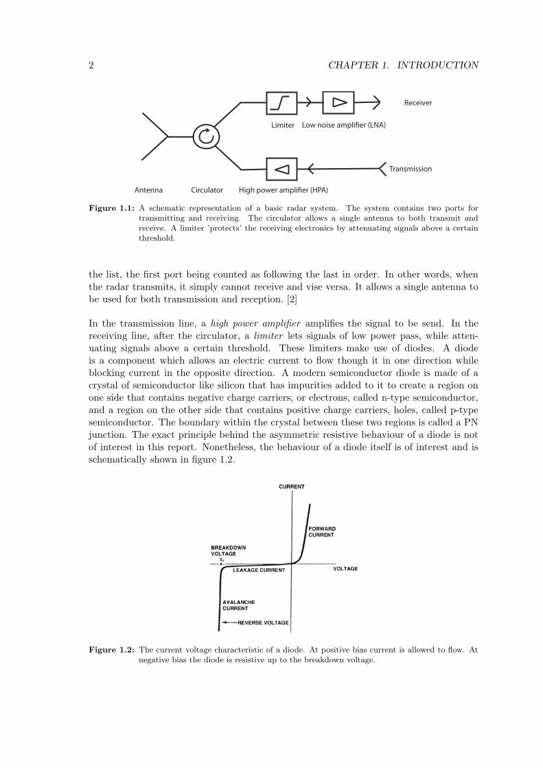
Figure 1.1 shows a schematic representation of a basic pulsed radar system, which cantransmit and receive a microwave pulse. [1]. Behind the antenna a circulator functions asa switch between transmitting and receiving. A circulator has multiple channels, in whichthe electromagnetic waves propagate from one channel to another only in a particularorder. It is a passive junction of in this case three ports in which the ports can be listedin such an order that when power is applied to any port it is transferred to the next on
1
2 CHAPTER 1. INTRODUCTION
Antenna Circulator
Limiter Low noise amplier (LNA)
High power amplier (HPA)
Transmission
Receiver
Figure 1.1: A schematic representation of a basic radar system. The system contains two ports fortransmitting and receiving. The circulator allows a single antenna to both transmit andreceive. A limiter ’protects’ the receiving electronics by attenuating signals above a certainthreshold.
the list, the first port being counted as following the last in order. In other words, whenthe radar transmits, it simply cannot receive and vise versa. It allows a single antenna tobe used for both transmission and reception. [2]
In the transmission line, a high power amplifier amplifies the signal to be send. In thereceiving line, after the circulator, a limiter lets signals of low power pass, while atten-uating signals above a certain threshold. These limiters make use of diodes. A diodeis a component which allows an electric current to flow though it in one direction whileblocking current in the opposite direction. A modern semiconductor diode is made of acrystal of semiconductor like silicon that has impurities added to it to create a region onone side that contains negative charge carriers, or electrons, called n-type semiconductor,and a region on the other side that contains positive charge carriers, holes, called p-typesemiconductor. The boundary within the crystal between these two regions is called a PNjunction. The exact principle behind the asymmetric resistive behaviour of a diode is notof interest in this report. Nonetheless, the behaviour of a diode itself is of interest and isschematically shown in figure 1.2.
Figure 1.2: The current voltage characteristic of a diode. At positive bias current is allowed to flow. Atnegative bias the diode is resistive up to the breakdown voltage.
3
The figure shows the non symmetrical behaviour of a common diode. At a forward voltage,the diode is conducting. At backward voltage the diode is resistive up to a certain point,were dielectric breakdown occurs and current is also flowing in the backward direction.This is the physical limit were the diode is permanently damaged.
Summarizing, diode based limiters have an important role in a radar system. The limitermakes sure the signal is weakened such that a signal is formed which can be analyzedby the electronics behind this ’protective wall’. Still, since limiters are based on diodes,there is a limit to its capacities. At a certain power, dielectric breakdown will occur, likelycausing irreversible damage to electronics behind the limiter in the receiving line.
Therefore, in collaboration with Thales Nederland BV, the following research field is pro-posed:
In the field of material science and nanotechnology, is it possible to develop materials whichintrinsically have a power dependence in their electrical and microwave response? Morespecific, a material, which on macroscopic scale would show power dependent response inits resistivity, and a power dependent reflective and transmissive response, increasing inreflection, decreasing in transmission, when subjected to microwaves.
A material which would fulfill these properties is a material, in which an intrinsic transitionfrom dielectric properties to metallic properties would occur, for an applied potential oran applied electromagnetic field. A dielectric material is obviously resistive, and for lowvalues dielectric values very transmissive for microwaves. A metal on the other hand isobviously very conductive and highly reflective for microwaves.
In fact, in an ideal situation, this material should show ’diode-like’ non linear behaviour.The material is resistive at low potential, but conducting for high potential. The same nonlinear behaviour for its response to microwaves. Transmissive at low power, reflective athigh power. A material which shows these types of non linear behaviour would create newpossibilities in limiters and controlling high electric fields and high power electromagneticradiation.
With this in mind, a literature study has shown that a material of great interest andpotential to show these non linear effect are based on percolative systems. Therefore,more specific, this research will focus on the electrical and microwave characterization ofcomposite material of an insulating embedding medium with metal filler particles.
First, chapter 2 will elaborate in more detail on the theoretical aspects on these percolativecomposite materials and the theory behind non linear resistive behaviour, resulting in theresearch questions. Next, the structural characterization of the composite material will beoutlined in chapter 3. Chapter 4 will subsequently discuss the sample preparation and ex-perimental setup to carry out a electrical DC characterization of the material, followed bythe outline of the sample preparation and experimental setup for the microwave character-ization of the composite material in chapter 5. Finally, conclusions and recommendationswill be presented in chapter 6.

4 CHAPTER 1. INTRODUCTION

Chapter 2
Theoretical background andresearch questions
As introduced, this research will focus on the electrical and microwave behaviour of com-posite material were conducting particles are embedded in an insulating epoxy matrix. Thethe potential of these systems to show non linear effects when submitted to a potential orelectromagnetic radiation is investigated.
These systems can be described as a percolative system described by percolation theories.First this chapter will elaborate more on these systems and their non linear resistivebehaviour due to varying filler ratio. Furthermore, literature will be discussed were theoryand measurements are compared, indicating field dependent resistive behaviour near thepercolation threshold caused by tunneling effects.
Subsequently, the general microwave response of materials will be discussed shortly. Also,literature describing permittivity measurements on composite material of filler particles isdiscussed.
Last, from this theory, the focus of the research will be discussed by proposing the researchgoals.
2.1 Percolation theory
In general, a composite of a medium with filler particles can be described as a mathematicalpercolative system based on theory of percolation. This theory describes the behaviourof connected clusters in a random medium. The composite material focus of this researchin particular consists of a insulating medium in which conducting metal particles areembedded. Hence, the resistivity of these models are described by this theory of thebehaviour of connecting clusters.
The electrical conductivity and dielectric constant, of metal-insulator mixtures, discussedlater on, are the most widely investigated physical properties of percolative systems [3]. Assaid, in general, a percolative system is described by the mathematical model of percolation
5

6 CHAPTER 2. THEORETICAL BACKGROUND AND RESEARCH QUESTIONS
theory. The main concept of percolation theory is the existence of a percolation thresholdfC , the filler ratio of clusters when connected paths between clusters start to occur. Inthe case of a composite of an insulating medium with conducting particles representingthe clusters, the resistance behaves very non linear.
Namely, when a certain amount of conductive filler is spread in an insulating polymermatrix, the material transforms from an insulator to a conductor. As the concentrationof the conducting additive is raised above fC , the number of continuous paths throughthe compound increases allowing conduction of charge carriers [4] [5] [6]. This resistivityas function of volume ratio filler material is shown in figure 2.1.
Re
sist
ivit
y
0 1
Volume fraction ller
fC
Figure 2.1: On the left, a schematic representation of the resistivity against volume fraction filler particles.At a certain volume particles tend to form linkages, resulting in a drastic drop in resistivity.The volume fraction at which this occurs is indicated by fC . On the right, an actual resistivitymeasurement on a composite of silver micro particles composite as a function of the microsilver particle volume fraction [7].
Percolation threshold values are usually in between 10-20% volume ratio filler particles,depending on the size of the filler particles [8] [7] [9].
2.2 Field dependent conductance
When the conductivity of a conductor-insulator composite is treated as a theoretical per-colation problem, for the conductivity of the composite, the following scaling law ap-plies [5]:
σdc ∝ (f − fC)t, (2.1)
with σdc the DC conductivity, f the filler ratio, fC the percolation threshold and t andarbitraty positive constant. Monte Carlo calculations in simulations of three dimensionshave shown that the value for t is about 1.6-2.0 [10].
Several experimental values of t measured in real systems like carbon black filled polymers,however, disagree with this theoretical value. When in a Monte Carlo experiment physicalcontact between conductive particles is needed to permit the conduction of the chargecarriers through the compound, in real conductor-insulator composites the electrons are
2.2. FIELD DEPENDENT CONDUCTANCE 7
allowed to tunnel from one conductive cluster to another separated by a thin insulatingpolymer layer. This is an indication that these materials, near percolation threshold, couldshow a conductivity dependent on the applied electric field.
This field dependence is verified in literature [11]. The relation between the resistanceand the filler volume ratio of these composites, as shown in figure 2.1, can be divided intothree regions. The first region shows a high resistivity at lower volume ratio. In the secondregion, the transition from insulator to metal occurs in a narrow span of increasing fillervolume ratio, were in the third region, the material is fully conducting.
It has been shown that the electric field dependence of current in the first region is ohmicand changes into a non-ohmic behavior in the second region. The third region shows anohmic current behavior again. The non-ohmic current behaviour and the sharp change inconductivity in the second region can be explained in terms of a tunneling conduction. Ithas to be noticed, that although the transition seems steep, there is a small span in fillerratio in which this transition occurs. At this filler ratio tunneling gaps exist, but a fullyconducting path is still not present. Therefore, when the composite is fully conductingand shows ohmic behaviour, actual percolation occurs, were conducting particles formconducting paths between contacts.
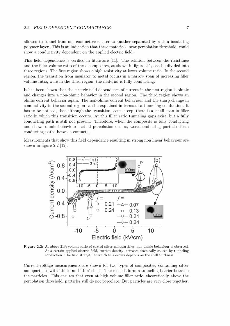
Measurements that show this field dependence resulting in strong non linear behaviour areshown in figure 2.2 [12].
Figure 2.2: At above 21% volume ratio of coated silver nanoparticles, non-ohmic behaviour is observed.At a certain applied electric field, current density increases drastically caused by tunnelingconduction. The field strength at which this occurs depends on the shell thickness.
Current-voltage measurements are shown for two types of composites, containing silvernanoparticles with ’thick’ and ’thin’ shells. These shells form a tunneling barrier betweenthe particles. This ensures that even at high volume filler ratio, theoretically above thepercolation threshold, particles still do not percolate. But particles are very close together,

8 CHAPTER 2. THEORETICAL BACKGROUND AND RESEARCH QUESTIONS
were the composite shows the non-ohmic behaviour. It can be seen that the composite withparticles with thin shell starts to conduct at 5kV/cm. For the thick shell, this obviouslyhigher, since the spacing between particles is bigger. Here, the material starts to conductat 10kV/cm. It is shown that this nonlinear behaviour is recoverable, which makes thesecomposite very interesting. This system in particular, consisting of silver nanoparticleswith a thin coating, has become focus of this research, which will be outlined in moredetail later on.
2.3 Microwave response materials
Besides the interest in non linear conductivity, focus of this research is also the microwaveresponse of these composites. This includes the reflective and transmissive behaviour ofthe material. As introduced, the composite material will experience a transition betweeninsulator and conductor. This obviously will affect its microwave response.
Measurements mainly have been carried out in a frequency span of 8-12GHz, or the X-band range, see appendix C. This because this is a commonly used frequency span inthe microwave industry, were these frequencies correspond with wavelengths in the orderof centimeters, which is from a practical point of view convenient in the construction ofmicrowave components.
Microwave response in conductors
At high filler ratio, the material acts metallic and conductive. Therefore, it will be veryreflective for microwaves. Basically, when an electromagnetic wave interacts with a con-ductive material, charges within the material are made to oscillate back and forth withthe same frequency as the fields. The movement of these charges, usually electrons, formsan alternating electric current, from which the magnitude is greatest at the conductor’ssurface. The decline in current density versus depth is known as the skin effect and theskin depth is a measure of the distance over which the current falls to 1/e of its originalvalue.
The skin depth is defined as the depth below the surface of the conductor at which thecurrent density decays to 1
e , about 0.37 of the current density at the surface, inducted bythe electromagnetic wave interacting with the surface of the conductor. The skin depthcan be calculated as follows:
δ =√
2ρωµ
, (2.2)
with ρ the resistivity of the conducting material, ω the angular frequency of the currentflowand µ the absolute magnetic permeability of the conductor. Permeability is the measure ofthe ability of a material to support the formation of a magnetic field within itself. In otherwords, it is the degree of magnetization that a material obtains in response to an appliedmagnetic field. Absolute permeability µ is equal to µ0 · µr, were µ0 is the permeability offree space equal to 4π ∗ 10−7NA−2 and µr the relative permeability of the conductor. Ata frequency of 10GHz, typical skin depth for silver is 0.64µm.

2.3. MICROWAVE RESPONSE MATERIALS 9
Microwave response in dielectrics
Different from conductors, dielectric or insulating materials do not only reflect electromag-netic waves, but partially will reflect, partially transmit waves, depending on the relativepermittivity εr, relative permeability µr, lossiness tanδ of the material and the frequencyof the electromagnetic waves.
Permittivity is the measure of how much resistance is encountered when forming an electricfield in a vacuum. In other words, permittivity is a measure of how an electric field affects,and is affected by, a dielectric medium. Permittivity is determined by the ability of amaterial to polarize in response to the field, and thereby reduce the total electric fieldinside the material. Thus, permittivity relates to a materials ability to transmit or ’permit’an electric field.
The relative permittivity of a homogeneous material is the permittivity relative to that offree space, also called dielectric constant, were εr = ε
ε0, with ε0 the permittivity of free
space with a value of ε0 ≈ 8.85 · 10−12. The relative permittivity is frequency dependentand complex, were εr(ω) = ε′r(ω) + iε′′r(ω).
Most influential on the microwave reflective behaviour of materials is the difference ofthe relative permittivity between two interfaces. A bigger difference in permittivity willresult in a higher reflection and less transmission. Since this research will examine thereflective and transmissive behaviour of a thin sample in between air, with the main focuson its reflective response, for a dielectric layer in between air, the reflection is expressedas [13]:
Figure 2.3: Schematic representation of a dielectric slab in between air.
R =R1 +R2e
−2γml
1 +R1R2e−2γml, (2.3)
with λm is the complex propagation constant in the layer of thickness l. Reflection andtransmission coefficients at the boundaries z = 0 and z = l are calculated trough thecharacteristic impedances or the corresponding media [1].
10 CHAPTER 2. THEORETICAL BACKGROUND AND RESEARCH QUESTIONS
R1 =Zm − Z0
Zm + Z0, R2 =
Z0 − ZmZ0 + Zm
(2.4)
The characteristic impedance of air is Z0 =√
µ0
ε0, the characteristic impedance of the
dielectric material is Zm = Z0
õr
ε′r−ε′′r. Loss of the material is defined as tanδ = ε,,
ε, . Thepropagation constant in the material is given as:
γm = jω√µ0ε0
√ε′r − jε′′r (2.5)
−12 −10 −8 −6 −4 −2 00
5
10
15
20
25
30
Reflection (dB)
ε r
8GHz
9GHz
10GHz
11GHz
12GHz
‘
Figure 2.4: Relation between the relative permittivity of a dielectric material and the reflection whensubjected to electromagnetic radiation in the microwave range.
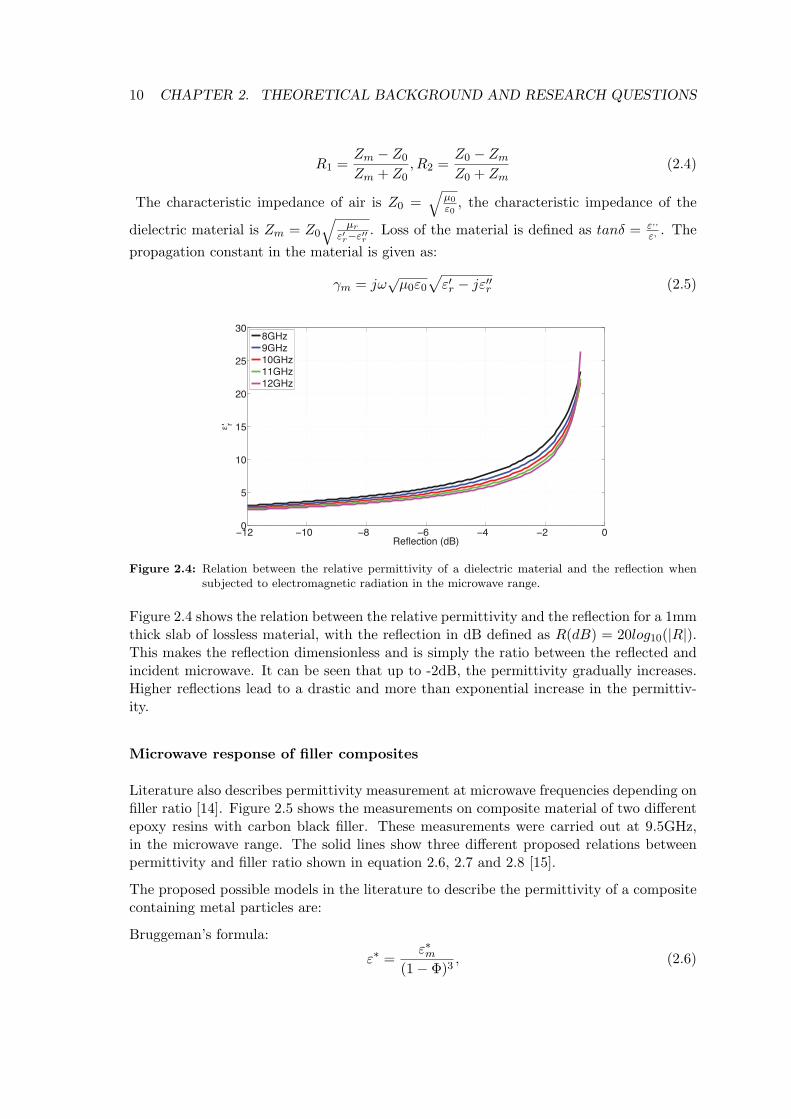
Figure 2.4 shows the relation between the relative permittivity and the reflection for a 1mmthick slab of lossless material, with the reflection in dB defined as R(dB) = 20log10(|R|).This makes the reflection dimensionless and is simply the ratio between the reflected andincident microwave. It can be seen that up to -2dB, the permittivity gradually increases.Higher reflections lead to a drastic and more than exponential increase in the permittiv-ity.
Microwave response of filler composites
Literature also describes permittivity measurement at microwave frequencies depending onfiller ratio [14]. Figure 2.5 shows the measurements on composite material of two differentepoxy resins with carbon black filler. These measurements were carried out at 9.5GHz,in the microwave range. The solid lines show three different proposed relations betweenpermittivity and filler ratio shown in equation 2.6, 2.7 and 2.8 [15].
The proposed possible models in the literature to describe the permittivity of a compositecontaining metal particles are:
Bruggeman’s formula:
ε∗ =ε∗m
(1− Φ)3, (2.6)

2.4. RESEARCH GOALS 11
Bruggeman
CorkumShin
Shin
Figure 2.5: The real part ε′r of the complex permittivity of carbon black epoxy resin composites as afunction of the volume concentration F at 9.5 GHz. Symbols indicate the measurements fortwo different epoxy resins. Solid lines show theoretical values referred to by the numbers ofequations with ε∗m = 3− i0.05.
Corkum’s equation:
ε∗ = ε∗m1 + 2Φ(1− Φ)
, (2.7)
Shin et al:
(ε∗)α =(1− Φ)(ε∗m)α
(1− ΦΦc
), (2.8)
with ε∗ = ε′r − jε′′r the relation between the relative permittivity and its real and complexpart of the composite material, ε∗m the complex relative permittivity of the embeddingmedium, Φ the filler ratio, α an arbitrary positive constant and ΦC the percolation thresh-old.
Clearly, all relations show a more or less exponential increase in permittivity with in-creasing filler ratio, were the percolation threshold is of influence. Especially the Shinmodel tends to increase dramatically near the percolation threshold. Therefore, researchon the possible power dependence of the reflectivity of conducting filler composite materialwith increasing filler volume ratio up to the percolation threshold, which has not yet beencarried out in literature, is of great interest.
2.4 Research goals
Considering the conductive characteristics of these composite materials: from theory, itis shown, that composite materials with conducting filler particles show interesting nonlinear conductive behaviour based on percolation theories. This non linearity is strictlyconnected to the filler ratio of conducting particles. It has also been shown that fielddependent nonlinear conductive behaviour occurs around the percolation threshold, wereparticles are close together but do not yet form connected paths. Since conductivity does

12 CHAPTER 2. THEORETICAL BACKGROUND AND RESEARCH QUESTIONS
not match percolation simulations, it is assumed that tunneling plays an important rolein the conductive behaviour around the percolation threshold. This field dependent nonlinear conductive behaviour based on tunneling effects has also been measured.
Considering the microwave characteristics of these materials: All these measurements de-scribed in literature are carried out at a constant microwave power. As shown, modellingmicrowave response of composite materials is always based on fits and assumptions, buthas never been very well understood. The power dependent microwave response systemsalso have never been investigated. Since these materials show interesting non linear fielddependent resistive behaviour when potential is applied, it has become of interest howthese materials would behave when subjected to various microwave powers. Possibly, dueto tunneling effect at the surface, near percolative composites could show non linear re-flective behaviour when subjected to certain high energy microwaves. This could be basedon induced currents between particles, creating conductive behaviour which makes thematerial more reflective.
Considering the composite material itself: These field dependent non linear effects willonly occur in non percolating systems. Non linear effect will very likely only be seen nearthe percolation threshold, were particles are close together, but do not form conductingpaths. Therefore, the composite material of interest consists of coated silver nanoparticlesembedded in an epoxy resin. The next chapter will elaborate more on this composite, fromwhich the production and characterization is part of the research.
The following research goals have been formulated:
• The fabrication of a composite material of coated silver nanoparticles in a insulatingepoxy resin. Analyzing particles for their composition and presence of a coating inthe first place, then creating homogeneous composite material with a defined varyingfiller ratio.
• Electrical characterization of this composite material. This includes resistance mea-surements and field dependence measurements, to investigate possible non linear fielddependent resistive behaviour.
• The microwave characterization of this composite material at varying conductivefiller ratio. This includes measuring the power dependent reflective and transmissivebehaviour of these composite materials, to investigate a possible power dependencein the reflective behaviour of the composite material. From these measurements thecalculation of the material parameters, relative permittivity εr, relative permeabilityµr and loss tangent tanδ.
Chapter 3
Structural characterization
As introduced, this research focuses on the electrical and microwave characteristics of silvernanoparticle composites. In general, a composite material is a material made from at leasttwo or more materials with significantly different physical or chemical properties. Again,the composite material of interest in this research is a material in which metallic silvernanoparticles are spread in an insulating epoxy resin at varying volume ratios.
This chapter first will outline the characterization of the used silver nanoparticles with theuse of Scanning Electron Microscopy (SEM), Transmission Electron Microscopy (TEM)and X-ray photoelectron spectroscopy (XPS). Next the fabrication and characterizationof the composite material will be discussed. This composite material will be used toconstruct various composite samples for DC and RF measurements outlined in the followingchapters.
Main questions in the structural characterization of the used commercially available silvernanoparticles and the composite material are:
• What is the exact size distribution of the particles?
• Do these nanoparticles have a ’coating’, and insulating thin shell around the metalliccore?
• If so, what is the shell thickness?
• Do the particles tend to cluster together as powder/part of composite?
• How do nanoparticles behave as part of a composite material when embedded in apolymer matrix of an epoxy resin, will these particles drift to the bottom, or willthey spread homogeneously?
3.1 Silver nanoparticles
As outlined in the previous chapter, the proposed ideal model for the composite consistsof a insulating matrix for which an epoxy resin is chosen filled with conducting fillerparticles with an insulating coating resulting in an insulating defined barrier between the
13
14 CHAPTER 3. STRUCTURAL CHARACTERIZATION
conducting particles, which prevents the particles from percolating at any ratio. As fillermaterial, silver nanoparticles are chosen, since silver is most conducting of all metals witha resistivity of 1.59 ∗ 10−8Ωm [16].
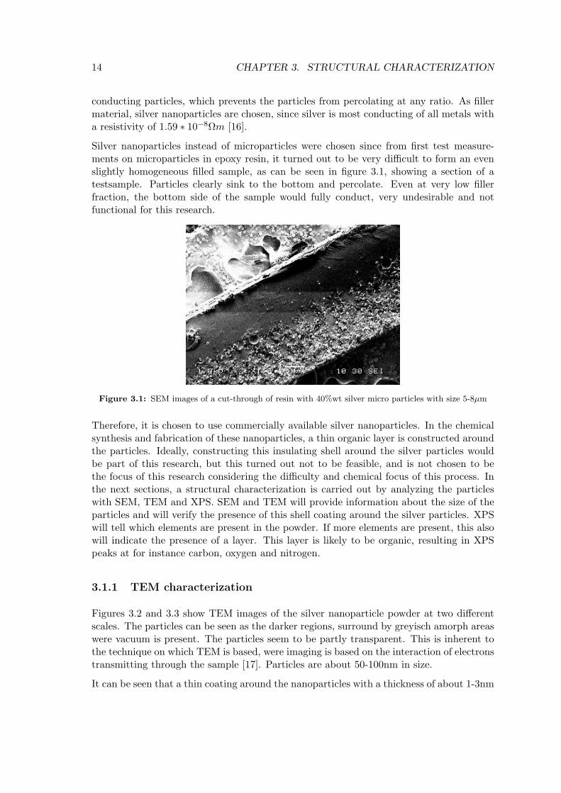
Silver nanoparticles instead of microparticles were chosen since from first test measure-ments on microparticles in epoxy resin, it turned out to be very difficult to form an evenslightly homogeneous filled sample, as can be seen in figure 3.1, showing a section of atestsample. Particles clearly sink to the bottom and percolate. Even at very low fillerfraction, the bottom side of the sample would fully conduct, very undesirable and notfunctional for this research.
Figure 3.1: SEM images of a cut-through of resin with 40%wt silver micro particles with size 5-8µm
Therefore, it is chosen to use commercially available silver nanoparticles. In the chemicalsynthesis and fabrication of these nanoparticles, a thin organic layer is constructed aroundthe particles. Ideally, constructing this insulating shell around the silver particles wouldbe part of this research, but this turned out not to be feasible, and is not chosen to bethe focus of this research considering the difficulty and chemical focus of this process. Inthe next sections, a structural characterization is carried out by analyzing the particleswith SEM, TEM and XPS. SEM and TEM will provide information about the size of theparticles and will verify the presence of this shell coating around the silver particles. XPSwill tell which elements are present in the powder. If more elements are present, this alsowill indicate the presence of a layer. This layer is likely to be organic, resulting in XPSpeaks at for instance carbon, oxygen and nitrogen.
3.1.1 TEM characterization
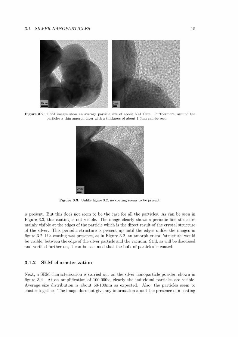
Figures 3.2 and 3.3 show TEM images of the silver nanoparticle powder at two differentscales. The particles can be seen as the darker regions, surround by greyisch amorph areaswere vacuum is present. The particles seem to be partly transparent. This is inherent tothe technique on which TEM is based, were imaging is based on the interaction of electronstransmitting through the sample [17]. Particles are about 50-100nm in size.
It can be seen that a thin coating around the nanoparticles with a thickness of about 1-3nm
3.1. SILVER NANOPARTICLES 15
Figure 3.2: TEM images show an average particle size of about 50-100nm. Furthermore, around theparticles a thin amorph layer with a thickness of about 1-3nm can be seen.
Figure 3.3: Unlike figure 3.2, no coating seems to be present.
is present. But this does not seem to be the case for all the particles. As can be seen inFigure 3.3, this coating is not visible. The image clearly shows a periodic line structuremainly visible at the edges of the particle which is the direct result of the crystal structureof the silver. This periodic structure is present up until the edges unlike the images infigure 3.2, If a coating was presence, as in Figure 3.2, an amorph cristal ’structure’ wouldbe visible, between the edge of the silver particle and the vacuum. Still, as will be discussedand verified further on, it can be assumed that the bulk of particles is coated.
3.1.2 SEM characterization
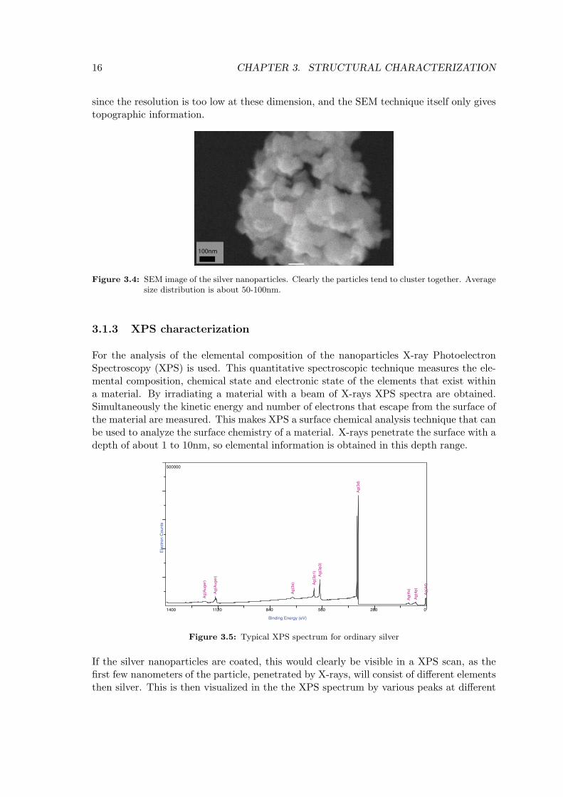
Next, a SEM characterization is carried out on the silver nanoparticle powder, shown infigure 3.4. At an amplification of 100.000x, clearly the individual particles are visible.Average size distribution is about 50-100nm as expected. Also, the particles seem tocluster together. The image does not give any information about the presence of a coating
16 CHAPTER 3. STRUCTURAL CHARACTERIZATION
since the resolution is too low at these dimension, and the SEM technique itself only givestopographic information.
100nm
Figure 3.4: SEM image of the silver nanoparticles. Clearly the particles tend to cluster together. Averagesize distribution is about 50-100nm.
3.1.3 XPS characterization
For the analysis of the elemental composition of the nanoparticles X-ray PhotoelectronSpectroscopy (XPS) is used. This quantitative spectroscopic technique measures the ele-mental composition, chemical state and electronic state of the elements that exist withina material. By irradiating a material with a beam of X-rays XPS spectra are obtained.Simultaneously the kinetic energy and number of electrons that escape from the surface ofthe material are measured. This makes XPS a surface chemical analysis technique that canbe used to analyze the surface chemistry of a material. X-rays penetrate the surface with adepth of about 1 to 10nm, so elemental information is obtained in this depth range.
Ele
ctr
on
Counts
Binding Energy (eV)
500000
1400 01120 840 560 280
Ag(A
uger)
Ag(3
s) Ag(3
p1)
Ag(4
s)
Ag(4
p)
Ag(4
d)
Ag(3
p3)
Ag(3
d)
Ag(A
uger)
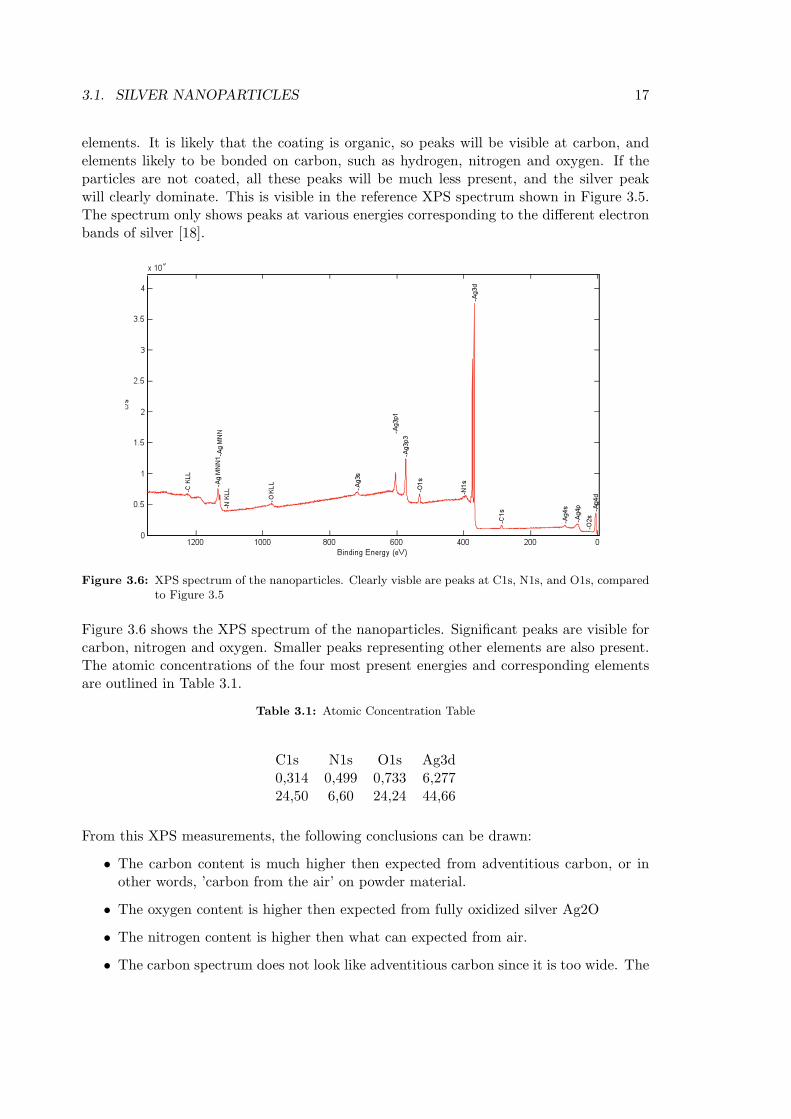
Figure 3.5: Typical XPS spectrum for ordinary silver
If the silver nanoparticles are coated, this would clearly be visible in a XPS scan, as thefirst few nanometers of the particle, penetrated by X-rays, will consist of different elementsthen silver. This is then visualized in the the XPS spectrum by various peaks at different
3.1. SILVER NANOPARTICLES 17
elements. It is likely that the coating is organic, so peaks will be visible at carbon, andelements likely to be bonded on carbon, such as hydrogen, nitrogen and oxygen. If theparticles are not coated, all these peaks will be much less present, and the silver peakwill clearly dominate. This is visible in the reference XPS spectrum shown in Figure 3.5.The spectrum only shows peaks at various energies corresponding to the different electronbands of silver [18].
Figure 3.6: XPS spectrum of the nanoparticles. Clearly visble are peaks at C1s, N1s, and O1s, comparedto Figure 3.5
Figure 3.6 shows the XPS spectrum of the nanoparticles. Significant peaks are visible forcarbon, nitrogen and oxygen. Smaller peaks representing other elements are also present.The atomic concentrations of the four most present energies and corresponding elementsare outlined in Table 3.1.
Table 3.1: Atomic Concentration Table
C1s N1s O1s Ag3d0,314 0,499 0,733 6,27724,50 6,60 24,24 44,66
From this XPS measurements, the following conclusions can be drawn:
• The carbon content is much higher then expected from adventitious carbon, or inother words, ’carbon from the air’ on powder material.
• The oxygen content is higher then expected from fully oxidized silver Ag2O
• The nitrogen content is higher then what can expected from air.
• The carbon spectrum does not look like adventitious carbon since it is too wide. The

18 CHAPTER 3. STRUCTURAL CHARACTERIZATION
high energy bands indicate carbon bound to oxygen.
• Zinc and Chlorine are found in small amounts. Maybe they are a part of the shellsurrounding the nanoparticles.
From the XPS measurement, it can be concluded that it is very likely that the particleshave an organic coating. The concentration of elements other then silver is much higher,than to be expected from contamination of the sample from elements in the air. One hasto take into account that, as said earlier, these concentration ratios do not apply for the’bulk’ of coated silver particles, as obviously, in the first few nanometers that the x-rayspenetrate the particle surface the beam only ’see’ the coating and no silver.
3.2 Composite of nanoparticles in epoxy resin
After the structural characterization of the silver nanoparticles, next step is to characterizethe behaviour of the silver particles embedded in an epoxy resin, with the goal to producea composite material in which silver particles are spread as homogeneous as possible, atvarying filler ratio.
Basically, constructing these composites is quite straight forward. A commercially availableresin is used, consisting of two mixtures of an epoxy embedding medium based on EPON812, the most widely used embedding resin for electron microscopy [19], with two differenthardeners, 2-dodecenylsuccinic anhydride (DDSA) and methylnadic anhydride (NMA).Two mixtures are made, one containing 5ml medium with 8ml DDSA, the second with8ml medium and 7ml NMA. After thorough magnetic stirring, these mixtures are pouredtogether and subsequently, 16 drops of 2,4,6-tris(dimethylaminomethyl)phenol (DPM-30)accelerator is added. Changing the ratio between the two mixtures wil influence thehardness and brittleness of the final product.
To make the final composite, a measured amount of silver particles is added to the epoxyresin mixture. This composite is then stirred by magnetic stirring. This gives the actualcomposite material with a certain volume ratio of silver particles.
To make samples, two types of molds that have been fabricated for the microwave mea-surements, more thoroughly discussed in chapter 5, are used. These molds are cured in anoven at an average temperature of 60C, while turning, to prevent particles from sinking.The aim is to create a composite with the conducting silver filler particles homogeneouslydispersed in the epoxy matrix. Therefore, it needs to be examined how the particles behavein the resin after the curing process. This includes:
• Particles drifting and settling on the bottom of the epoxy matrix
• Distribution of particles through the epoxy matrix
• Possible clustering of particles
Therefore, SEM images are taken from sections of test samples, discussed in the nextsection.

3.2. COMPOSITE OF NANOPARTICLES IN EPOXY RESIN 19
3.2.1 SEM characterization
First, test samples are created by filling a X-band mold with the liquid composite material,resulting in samples with a thickness of about 1mm. Again, the fabrication of this moldand samples will be discussed more thoroughly in section 5.2.1 and is not yet of interest inthis section. To analyze possible sinking of particles, a low volume filler ratio of 5% silverparticles is chosen. SEM images of sections of the sample are shown in figure 3.7.
200μm10μm
Figure 3.7: SEM images of a section of a test sample with a 5% silver particle filler volume ratio at twodifferent scales. Macroscopically, the particles seem to have spread homogeneously in thematerial, as can be seen on the left. No particle sinking is present, which would result in aclear visible gradient in contrast in the image. Microscopically, the particles cluster, as canbe seen on the right.
1mm 50μm
10μm
Figure 3.8: A film of the composite dropped and cured on a thin gold layer sputtered on a silicon substrate.Silver particles are spread microscopically.
It can be seen that this sample fabrication method leads to macroscopically homogeneoussamples, as no significant contrast gradient is present in the section of the samples. Thisindicates that particles did not sink to one side of the sample, but spread homogeneouslythrough the sample. Microscopically, particles still tend to cluster.
20 CHAPTER 3. STRUCTURAL CHARACTERIZATION
For the DC measurements outlined in the next chapter, a drop of composite material witha high volume filler ratio of 25% is put on top of a substrate, resulting in a thin layer ofcomposite material. To examine structural behaviour of this thin film of composite, a testsample is created were a drop of composite material with a filler ratio of 25% is put on topof a gold sputtered silicon substrate. After curing, the film is scratched to be able to makeSEM images of a section of the composite thin film. The SEM images are shown in Figure3.8. Clearly, also here, the macroscopically, the particles are spread homogeneously, butmicroscopically also cluster.
3.2.2 Conclusions structural characterization
This chapter outlined the structural characterization of commercially available silver nanopar-ticles and the composite material that has been constructed from these particles embeddedin a commercially available epoxy embedding resin. The main questions proposed werethe following:
• What is the exact size distribution of the particles?
• Do these nanoparticles have a ’coating’, and insulating thin shell around the metalliccore?
• If so, what is the shell thickness?
• Do the particles tend to cluster together as powder/part of composite?
• How do nanoparticles behave as part of a composite material when embedded in apolymer matrix of an epoxy resin, will these particles drift to the bottom, or willthey spread homogeneously?
With the use of SEM, TEM and XPS it can be concluded that the average size of theparticles is about 50-100nm. Also is very likely that these particles have some form oforganic coating, with an average thickness of about 3nm. Considering the method inwhich these particles are made chemically, namely a synthesis in an organic solution, thesecharacterization verifies the expected presence of a coating.
Still, it is questionable whether all particles are individually coated. TEM images alsoshowed particles that very likely were not coated. But considering the XPS measurementand the synthesis of these powders, it may be assumed that the bulk of the particles iscoated, which makes these particles useful in the suggested model of non percolating spacedmetallic particles in an insulating matrix of epoxy resin.
Next, test samples from the composite material are constructed and examined with SEM.It is shown that with the proposed fabrication technique silver particles spread macroscop-ically homogeneous through the epoxy without sinking to one side. Also, for increasingfiller ratio, the density of silver particles also increased homogeneously. Microscopically,the particles do tend to cluster, but again, are very likely to experience an average spacingdue to the coating. This prevents clustering and makes the composite samples useful forthe DC and microwave measurements, outlined in the next chapters.

Chapter 4
Electrical DC characterization
In this chapter the DC electrical properties of the composite material are examined. First,a basic setup is constructed to measure the resistance of bulk composite material at highvolume ratio silver nanoparticle filler material. This will provide information about thepresence of an insulating shell around the metal particles. Next, the electrical propertieson microscopic scale are examined. Herefore, substrates are used on which gold contactsare sputtered with a spacing of only a few micrometer. By depositing the compositematerial on these contacts, a more quantitative approach can be used to describe thesystem, since a quantified amount of particles is positioned in between the contacts. Byapplying a potential sweep on the contacts, the current and resistance response of thecomposite material is examined and whether non linear behaviour as described in literatureis observed.
4.1 Resistance measurements on bulk composite
As described in the theory, composite materials containing metallic particles show a distincttransition with increasing particle filler ratio, from an insulating to a conducting material.From theory, this transition occurs at a filler volume percentage of about roughly 10-20%. Above this filler ratio, particles percolate creating conducting paths which drasticallyincreases conductivity of the material.
As introduced in the previous chapter, it is very likely that the used silver nanoparti-cles used in this research have an thin organic insulating shell. Theoretically this wouldmean, that a composite, with a volume filler particles higher then the volume at whichtheoretically percolation occurs, would still be insulating. Therefore, a rough resistancecharacterization is carried out on a composite with a volume filler ratio of 25%, above thepercolation volume percentage.
To carry out this measurement, a drop of composite material is deposited on a thin goldlayer of about 200nm sputtered on a silicon substrate. At various points on the compositelayer conducting silver glue contacts are constructed, so resistance is measured at multiplespots. Also contacts are constructed on the gold layer. A schematic representation of the
21

22 CHAPTER 4. ELECTRICAL DC CHARACTERIZATION
setup is shown in figure 4.1. A section through a contact is shown in figure 4.2. Clearly,the ’blob’ of silver glue can be seen on top of a layer of composite material with a thicknessof about 200µm. The smooth dark region left from the layer of composite material is thegold layer. It has to be taken in mind that the whole sample is tilted slightly, were theSEM is actually looking on top of the gold layer, were there is a 90 angle between thegold and composite layer.
Silver glue
Composite
AU
SI
Figure 4.1: Schematic representation of the macroscopic two-point measurements
With a multimeter, initial resistance on all the contacts was measured. It immediately be-came clear that the composite was fully resistive. No value was measured, which indicatesthat the resistance of the composite is out of range of the multimeter which measures re-sistance up to 107Ω. Considering the volume filler ratio of 25%, higher then the theoreticalpercolation volume, this is a clear indication of the presence of a insulating shell aroundthe silver nanoparticles which prevents the particles from percolating.
200μm 50μm
Figure 4.2: A section of the composite on gold sample, cut through in the middle of the silver glue, afterthe voltage sweep measurements. Although the dielectric breakdown indicates a intrinsicchange in the material, no structural change is observed with SEM. This is to be expected,as this dielectric breakdown likely has occured very locally in the material.
Next, voltage sweep measurements have been carried out by connecting the contacts toa Keithley potentiometer. These sweep measurements started at an initial voltage of 5V,were resistance immediately irreversibly dropped to a few Ohms, very likely indicating animmediate dielectric breakdown. It can be concluded that the composite clearly respondson an applied voltage. Likely by heating, the material locally intrinsically changes, causinga percolating path, which results in a local drop of the resistance.
New measurements at better control of the voltage sweeps were not carried out by the

4.2. MICROSCOPIC ELECTRICAL CHARACTERIZATION COMPOSITE 23
lack of new samples, this is a recommendation for further research to the electrical bulkbehaviour of the composite.
Figure 4.2 shows the SEM images of sections of the sample taken after the voltage sweepmeasurements. No structural change is visible. But a dielectric breakdown could easilyhave taken place in a different part of the sample since the path for breakdown can bevery local.
4.2 Microscopic electrical characterization composite
The measurements described above are very qualitative of nature. Possible non lineareffects of these materials are better to be examined on a smaller scale, with a more quan-titative approach. If conductivity is measured through a quantified amount of particlesmore quantitative information of the conductivity of the composite material is obtained.Therefore, a new setup is constructed to measure conductivity of the composite more lo-cally. The following sections will describe the used substrate and measurements on thecomposite.
4.2.1 Sample preparation, experimental setup
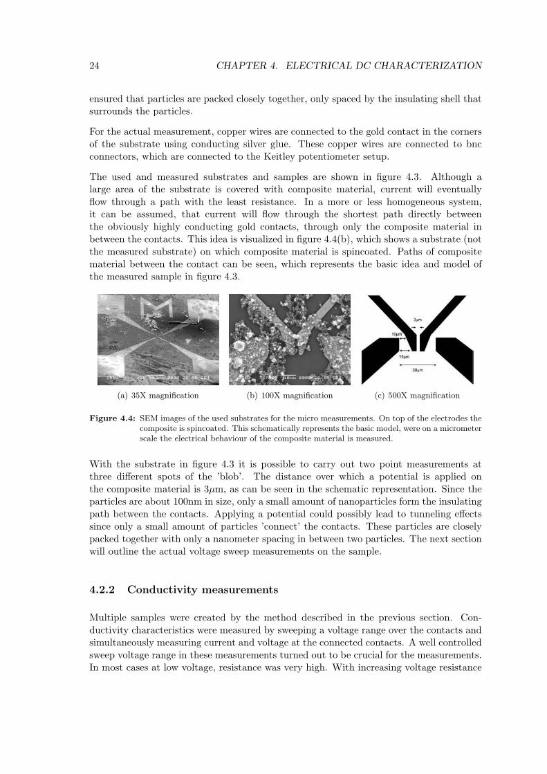
To carry out conductivity measurements on a smaller scale, substrates are used on whichgold microscopic structures are sputtered specific for carrying out two and four pointmeasurements. These substrates have four contact points in the corners of the about0.25cm2 large Si with SiO2 terminated substrates. These contacts are connected to amicroscopic gold structure in the middle of the sample with a slight spacing of a fewmicrometer between each contact. A schematic example of the structure on a substrate isgiven in figure 4.3(a) and 4.4(c).
(a) Schematic representation ofmicro contacts on the substrate
500μm
(b) SEM image of a ’blob’ of compositecovering the substrate
(c) Schematic representation ofthe experimental setup
Figure 4.3: The used substrate for the microscopic electrical measurements with dimensions given. Atwo-point voltage sweep is carried out over two connected contacts, as can be seen in theschematic figure on the right.
On the substrate, a ’blob’ of composite material with a 25% volume fraction of silvernanoparticles is dropped on the gold contacts, as indicated in Figure 4.3(b). The volumeratio of 25% is chosen since it is higher then the percolation volume ratio. Therefore, it is
24 CHAPTER 4. ELECTRICAL DC CHARACTERIZATION
ensured that particles are packed closely together, only spaced by the insulating shell thatsurrounds the particles.
For the actual measurement, copper wires are connected to the gold contact in the cornersof the substrate using conducting silver glue. These copper wires are connected to bncconnectors, which are connected to the Keitley potentiometer setup.
The used and measured substrates and samples are shown in figure 4.3. Although alarge area of the substrate is covered with composite material, current will eventuallyflow through a path with the least resistance. In a more or less homogeneous system,it can be assumed, that current will flow through the shortest path directly betweenthe obviously highly conducting gold contacts, through only the composite material inbetween the contacts. This idea is visualized in figure 4.4(b), which shows a substrate (notthe measured substrate) on which composite material is spincoated. Paths of compositematerial between the contact can be seen, which represents the basic idea and model ofthe measured sample in figure 4.3.
(a) 35X magnification (b) 100X magnification (c) 500X magnification
Figure 4.4: SEM images of the used substrates for the micro measurements. On top of the electrodes thecomposite is spincoated. This schematically represents the basic model, were on a micrometerscale the electrical behaviour of the composite material is measured.
With the substrate in figure 4.3 it is possible to carry out two point measurements atthree different spots of the ’blob’. The distance over which a potential is applied onthe composite material is 3µm, as can be seen in the schematic representation. Since theparticles are about 100nm in size, only a small amount of nanoparticles form the insulatingpath between the contacts. Applying a potential could possibly lead to tunneling effectssince only a small amount of particles ’connect’ the contacts. These particles are closelypacked together with only a nanometer spacing in between two particles. The next sectionwill outline the actual voltage sweep measurements on the sample.
4.2.2 Conductivity measurements
Multiple samples were created by the method described in the previous section. Con-ductivity characteristics were measured by sweeping a voltage range over the contacts andsimultaneously measuring current and voltage at the connected contacts. A well controlledsweep voltage range in these measurements turned out to be crucial for the measurements.In most cases at low voltage, resistance was very high. With increasing voltage resistance

4.2. MICROSCOPIC ELECTRICAL CHARACTERIZATION COMPOSITE 25
tended to drop drastically, indicating a breakdown in the sample, similar to the macro-scopic behaviour outlined in the previous section. When the same sweep was repeated,the resistance remained at low values, indicating a non reversible, non reproducible be-haviour.
10−4
10−3
10−2
10−1
100
101
102
10−14
10−12
10−10
10−8
10−6
10−4
10−2
Sweep voltage (V)
Current (I)
1st measurement2nd measurementClean substrateShorted substrate
Figure 4.5: Current Voltage characteristic
But in more controlled voltage sweeps it was achieved to measure non linear reversiblebehaviour. Figure 4.5 and 4.6 show a two point conductivity measurement on. Again,in this measurement, a composite with a silver particle filler ratio of 25% is deposited ona substrate as shown in Figure 4.3, where two of the four contacts are connected to apotentiometer.
10−3
10−2
10−1
100
101
104
105
106
Sweep Voltage (V)
Re
sis
tan
ce
(R
)
1st measurement2nd measurement
Figure 4.6: Resistance Voltage characteristic
The graphs shows two different voltage sweeps which were carried out in sequence. Thefirst measurement shows a linear sweep from 0.01V to 1V and back, which is shown bythe two red lines. The sweep starts at 0.01V, increases up to 1V, then decreases againto 0.01V. It can be seen that both paths do not overlap exactly, which indicates that thematerial is slightly altered in its non linear resistive response. After the sweep sampleturns out to be a bit less resistive. But qualitatively, the material shows a clear voltage

26 CHAPTER 4. ELECTRICAL DC CHARACTERIZATION
dependent non linear response.
The second sweep, indicated in blue, is carried out subsequent to the first. Interesting isthe fact that the initial resistance is a little bit higher again, than at the end of the firstmeasurement. This means that the material ’recovered’ over time. Instead of the first’two-way’ sweep, this measurement is just a ’one-way’ sweep in a wider range of 0.001V to15V. Again, a drop can be seen, only this time at a higher voltage. But again, qualitatively,the same non linear behaviour is observed.
A reference measurement on a clean substrate and a measurement in which the two contactare shorted with silver glue are also shown in figure 4.5. Since the measurements withthe composite are in between these two measurements, it is clear that the compositematerial has a non linear influence on the conductivity between the contacts. And also,the behaviour is reversible, since qualitatively, this behaviour appears in two individualsweep measurements. Although the two sweeps don’t match perfectly, they roughly overlapshowing qualitatively the same behaviour indicating that this behaviour is intrinsic to thematerial.
4.3 Conclusions electrical DC characterization
In this chapter the DC conductivity measurements on bulk scale and micro scale wereoutlined. On bulk scale no current voltage characteristics were determined due to lackingexperience with the experimental setup. High voltages were applied on the sample whichin all cases led to dielectric breakdown of the sample. Though, is was shown, that sampleswith high volume ratio filler material, well above the theoretical percolation threshold vol-ume, were initially resistive. This indicates the presence of the insulating shell around thesilver nanoparticles. Measurements on micro scale were carried out using substrates witha gold sputtered structure which can be used to do four point and two point measurement.After test runs to control the range of the voltage sweep interesting data was obtained ina two point measurement. In this setup, the current voltage characteristic of a compositewith a volume fraction of silver nanoparticles of 25% was determined. This measurementqualitatively showed reproducible non linear behaviour of the material.
Basically at this point we can conclude:
• It can be assumed that the bulk of particles is coated as the samples in the macro-scopic and microscopic measurements were insulating at first, even at a high volumeratio of silver particles were percolation is expected.
• In the microscopic measurements, reversible reproducible non linear behaviour in-trinsic to the composite material is seen. This effect, considering literature, is verylikely the result of tunnel effects between particles close together. It is shown thata rather simple fabrication method, were nanoparticles are stirred in liquid epoxy,show great potential in power dependent non linear resistive behaviour. This ismainly caused by the fact that particles are coated, were a high filler volume, overthe theoretical percolation threshold, will not lead to percolation, but a very closepacking of particles is preserved.

4.3. CONCLUSIONS ELECTRICAL DC CHARACTERIZATION 27
• Measurements are very qualitative in form. Qualitative non linear behaviour hasbeen shown, but the system is still very undefined. Tunneling is propably the mostimportant conduction mechanism, but this can only be verified when the actualpath with a certain amount of filler particles, over which the voltage is applied, isquantified. In such a system, the conductive response could be controlled better.Still, the measured system with composite on microparticles has shown to be a setupvery useful to analyse this non linear behaviour.

28 CHAPTER 4. ELECTRICAL DC CHARACTERIZATION
Chapter 5
Microwave characterization
In this chapter, various microwave measurements on the samples made from the compositematerial of silver nanoparticles in an epoxy resin matrix are outlined. First, ’coaxial’measurements have been carried out. In a coaxial sampleholder setup connected to a two-port network analyzer the frequency depending reflection and transmission response for arange of samples with varying ratios of silver particles is determined. Software calculationshave been carried out to determine the material parameters of the samples.
Next, ’X-band’ measurements have been carried out. Herefore, new samples of varyingfiller ratio have been constructed with X-band waveguide dimensions. First, the frequencydependent reflective and transmissive behaviour of these samples is measured in a two-port network analyzer setup. Subsequently, a Thales Matlab model for calculating thereflection and transmission response in a waveguide setup is fitted to these measurements,resulting in material parameters for comparison with the coaxial measurements.
Last, the X-band waveguide setup is measured in a ’high power’ setup, in which thefrequency depending reflection coefficients of the X-band samples for a range of poweroutput is determined.
5.1 Coaxial measurements
The first microwave measurements on the composite material of epoxy resin filled with avarying ratio of silver nanoparticles are carried out in a coaxial network analyzer setup.With this setup, the dielectric constant, or permittivity εr and the permeability µr of thecomposite material can be determined. This section will outline the preparation of thesamples, the experimental setup that is been used and the measurements that have beencarried out. Subsequently, the material parameters calculated from these measurements,are outlined and discussed.
29

30 CHAPTER 5. MICROWAVE CHARACTERIZATION
5.1.1 Sample preparation and experimental setup
To carry out the coaxial microwave measurements, samples have to be constructed thatfit the experimental setup. The experimental setup requires samples with very accuratedimensions. Samples need to be cylindrically shaped, with an inner diameter of 3.03mmand an outer diameter of 7.01mm. The thickness of the sample may vary, but has to beat least 1mm. These dimensions have to be precise, since the samples has to fit in themeasurement setup as tightly as possible. This because leakage will influence the materialparameter calculations, as will be discussed in section 5.1.4.
To create samples with these dimensions as accurate as possible, teflon sample holders,displayed in figure 5.1, are created with the use of a lathe.
3.03mm
7.01mm
Figure 5.1: Schematical representation of the teflon mold in which the coaxial samples are made.
These molds are filled with the liquid composite with varying silver filler ratio. Subse-quently, a teflon ’lid’ is tightened on top of the mold. Then, the filled molds are put ina vacuum, to remove excessive air which could lead to air holes. Next, all the molds areput in a plastic cup which is attached to a stirrer, inside an oven. Hereby, the samples arecured, while tumbling around, which prevents particles from sinking.
When removed from the mold, samples look smooth and homogenous, but small air bubblesare present. The influence of these bubbles on measurements will be discussed in section5.1.2.
A schematic overview of the measurement setup is displayed in figure 5.2. A copper hollowcylinder is put into the hole in the sample. Then, the sample is placed in a cylindricalcutout in a piece of copper, with a diameter of about 7mm, as can be seen in figure 5.2(a).A copper ’lid’ with the same cutout is then placed on top, fixing the sample in place. Twoconnectors are screwed on each side of the sampleholder.
These connectors are connected to two ports of a network analyser, as can be seen infigure 5.2(b), which is set to an output power of 10dBm. In this way, a so-called scattermatrix or S-matrix is obtained. A scatter matrix contains the reflection and transmissioncoefficients over a frequency span, on the two ports of the network analyser. This sweepruns from 100MHz to 18.2GHz with 100MHz steps, covering various microwave frequencybands.
For a two-port setup, this S-matrix will contain four parameters,(Sxx SxySyx Syy
), where x
and y corresponds with respectively port one and port two of the network analyzer. Hence,

5.1. COAXIAL MEASUREMENTS 31
(a)
Port 1 Port 2
S11 S22
S21
S12
DUT
NA
(b)
Figure 5.2: A schematic representation of the sample holder and the experimental setup for the coaxialmeasurements is shown. Figure 5.2(a) shows the sample holder, with the silver/epoxy sampleshown in grey. Figure 5.2(b) shows this Device Under Test (DUT) connected to a two portNetwork Analyzer (NA).
S11 and S22 correspond to the reflective signal of respectively port one and two, were S12
and S21 correspond to the transmitted signal between port one and two [20].
The value of the coefficients indicates the ratio between the outcoming signal to the incom-ing signal in decibel (dB). For instance, when S11 equals -1dB, the measured reflection, orincoming signal at port one is 1dB weaker then the outputted signal by port 1. Reflectivematerial, such as metals, will obviously show high reflection coefficients. Vice versa is thecase for low reflective materials, such as epoxy resins.
To determine the material parameters from the measurements, the dielectric constant orpermittivity εr and the permeability µr, the network analyser is coupled to software whichmakes a readout of the network analyzer measurements. Subsequenlty, a fitting algorithmin the software translates the S-matrix data to values for the real and complex part of thepermittivity and permeability, ε′(ω), ε′′(ω), µ′(ω) and µ′′(ω), of the composite material.The material parameters depend on parameters such as the thickness of the sample andthe ’fitmargins’ of the sample inside the sample holder in the case of small spacings be-tween sample and holder. To carry out these fitting calculations, these depending fittingparameters need to be defined in the software.
5.1.2 Measurements
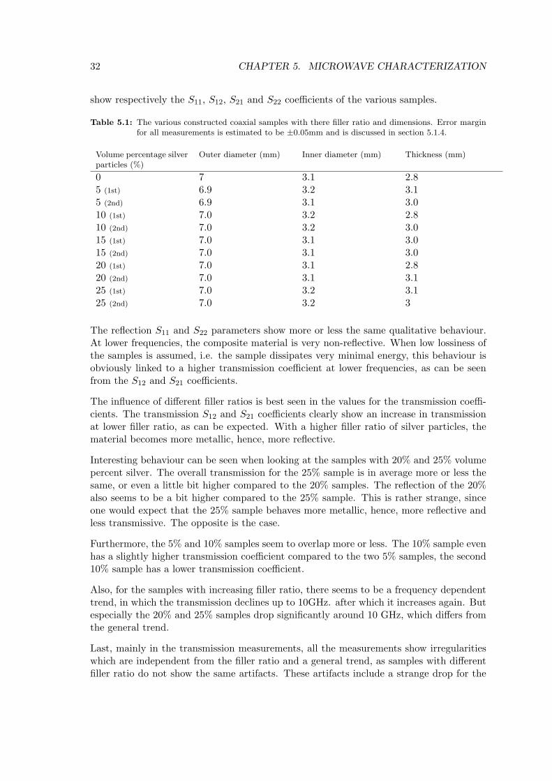
A total of eleven samples is measured in the described experimental setup. These elevensamples contain one sample with a zero filler ratio, a sample purely constructed of epoxyresin. The other ten samples are divided in two samples per filler ratio. The used ratiosare 5%, 10%, 15%, 20% and 25% volume percentage silver nanoparticles. In table 5.1,the dimensions of the samples are outlined. These dimensions are of critical value in thecalculations of the material parameters, as will be discussed later on.
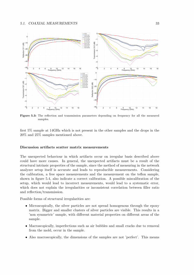
First, as can be seen in figure 5.3, the reflection and transmission scattermatrix measure-ments on all samples is shown. From the upper left to the lower right, the four graphs
32 CHAPTER 5. MICROWAVE CHARACTERIZATION
show respectively the S11, S12, S21 and S22 coefficients of the various samples.
Table 5.1: The various constructed coaxial samples with there filler ratio and dimensions. Error marginfor all measurements is estimated to be ±0.05mm and is discussed in section 5.1.4.
Volume percentage silverparticles (%)
Outer diameter (mm) Inner diameter (mm) Thickness (mm)
0 7 3.1 2.85 (1st) 6.9 3.2 3.15 (2nd) 6.9 3.1 3.010 (1st) 7.0 3.2 2.810 (2nd) 7.0 3.2 3.015 (1st) 7.0 3.1 3.015 (2nd) 7.0 3.1 3.020 (1st) 7.0 3.1 2.820 (2nd) 7.0 3.1 3.125 (1st) 7.0 3.2 3.125 (2nd) 7.0 3.2 3
The reflection S11 and S22 parameters show more or less the same qualitative behaviour.At lower frequencies, the composite material is very non-reflective. When low lossiness ofthe samples is assumed, i.e. the sample dissipates very minimal energy, this behaviour isobviously linked to a higher transmission coefficient at lower frequencies, as can be seenfrom the S12 and S21 coefficients.
The influence of different filler ratios is best seen in the values for the transmission coeffi-cients. The transmission S12 and S21 coefficients clearly show an increase in transmissionat lower filler ratio, as can be expected. With a higher filler ratio of silver particles, thematerial becomes more metallic, hence, more reflective.
Interesting behaviour can be seen when looking at the samples with 20% and 25% volumepercent silver. The overall transmission for the 25% sample is in average more or less thesame, or even a little bit higher compared to the 20% samples. The reflection of the 20%also seems to be a bit higher compared to the 25% sample. This is rather strange, sinceone would expect that the 25% sample behaves more metallic, hence, more reflective andless transmissive. The opposite is the case.
Furthermore, the 5% and 10% samples seem to overlap more or less. The 10% sample evenhas a slightly higher transmission coefficient compared to the two 5% samples, the second10% sample has a lower transmission coefficient.
Also, for the samples with increasing filler ratio, there seems to be a frequency dependenttrend, in which the transmission declines up to 10GHz. after which it increases again. Butespecially the 20% and 25% samples drop significantly around 10 GHz, which differs fromthe general trend.
Last, mainly in the transmission measurements, all the measurements show irregularitieswhich are independent from the filler ratio and a general trend, as samples with differentfiller ratio do not show the same artifacts. These artifacts include a strange drop for the
5.1. COAXIAL MEASUREMENTS 33
0 2 4 6 8 10 12 14 16 18−50
−40
−30
−20
−10
0
Frequency (GHz)
Reflection S11 (dB)
0.000.05 (1st)0.05 (2nd)0.10 (1st)0.10 (2nd)0.15 (1st)0.15 (2nd)0.20 (1st)0.20 (2nd)0.25 (1st)0.25 (2nd)
0 2 4 6 8 10 12 14 16 18−6
−5
−4
−3
−2
−1
0
Frequency (GHz)
Transmission S12 (dB)
0 2 4 6 8 10 12 14 16 18−6
−5
−4
−3
−2
−1
0
Frequency (GHz)
Transmission S21 (dB)
0.000.05 (1st)0.05 (2nd)0.10 (1st)0.10 (2nd)0.15 (1st)0.15 (2nd)0.20 (1st)0.20 (2nd)0.25 (1st)0.25 (2nd)
0 2 4 6 8 10 12 14 16 18−50
−40
−30
−20
−10
0
Frequency (GHz)
Reflection S22 (dB)
Figure 5.3: The reflection and transmission parameters depending on frequency for all the measuredsamples.
first 5% sample at 14GHz which is not present in the other samples and the drops in the20% and 25% samples mentioned above.
Discussion artifacts scatter matrix measurements
The unexpected behaviour in which artifacts occur on irregular basis described abovecould have more causes. In general, the unexpected artifacts must be a result of thestructural intrinsic properties of the sample, since the method of measuring in the networkanalyzer setup itself is accurate and leads to reproducible measurements. Consideringthe calibration, a free space measurements and the measurement on the teflon sample,shown in figure 5.4, also indicate a correct calibration. A possible miscalibration of thesetup, which would lead to incorrect measurements, would lead to a systematic error,which does not explain the irregularities or inconsistent correlation between filler ratioand reflection/transmission.
Possible forms of structural irregularities are:
• Microscopically, the silver particles are not spread homogenous through the epoxymatrix. Bigger and smaller clusters of silver particles are visible. This results in a’non symmetric’ sample, with different material properties on different areas of thesample.
• Macroscopically, imperfections such as air bubbles and small cracks due to removalfrom the mold, occur in the sample.
• Also macroscopically, the dimensions of the samples are not ’perfect’. This means

34 CHAPTER 5. MICROWAVE CHARACTERIZATION
that there are spacings between the edges of the samples with the sample holder.These spacings vary per sample, as shown in table 5.1.
The presence of the first two possible forms is verified after analyzing cuts of each samplewith Scanning Electron Microscopy (SEM). Back-Scattered Electron (BSE) and SecondaryElectron Imaging (SEI) images were taken, shown in appendix E.1. These images clearlyshow the irregular presence of small air bubbles. Also it can be seen that on a macroscopiclevel, the composite material is rather homogeneous, bigger and smaller clusters of silverparticles are spread homogeneously. But as said, on a microscopic level, the compositeis inhomogeneous, particles are clustered together. The dimensional misfit of the samplesis simply determined by measuring the samples with a micrometer. The misfit obviouslypresent, as indicated in table 5.1, were a perfect sample would have a inner diameter of3.04mm and an outer diameter of 7mm.
Intuitively, the first two types of irregularities mainly effect the ’smoothness’ of the mea-surement, and are the reason for the irregularities in the measurement in for instance the5%, 20% and 25% samples. The drops at 10GHz for the 20% and 25% samples can beseen in both samples, so are not completely irregular. Still the first two causes could bethe reason for these drops, since all sample were constructed in the same way. Therefore,a same amount of ’lack of homogenity’ could be present in both sets of samples.
To verify this cause of micro and macroscopic irregularities leading to a less smooth mea-surement , a measurement has been carried out on a perfect homogenous sample. It showsa more smooth measurement, as can be seen in figure 5.4. This figure shows the scat-ter matrix parameters and the dielectric constant and loss tangent. Again, the differencebetween the composite and teflon is the micro and macroscopic inhomogeneities in thecomposite, concluding that these types of inhomogeneities are therefore very likely to havecaused the irregularities in the measurements.
Discussible is whether the macroscopic air bubbles contribute in the presence of the irreg-ularities. Also the 0% sample has bubbles, but shows a rather smooth measurement. Thismight indicate that microscopic inhomogeneities in the spread of silver particles are themain cause for the irregularities.
0 2 4 6 8 10 12 14 16 18−50
−40
−30
−20
−10
0
Frequency (GHz)
dB
S11S22S12S21
(a)
0 5 10 150
0.5
1
1.5
2
2.5
3
Frequency (GHz)
a.u
.
εr
tanδ
(b)
Figure 5.4: Scatter matrix of a teflon sample plotted left, its permittivity and loss tangent plotted on theright.

5.1. COAXIAL MEASUREMENTS 35
The third form of imperfection, the dimensional misfit of samples is the most plausibleexplanation for some samples having an overall higher transmission then expected. If thesample does not fit perfectly in the sample holder, there will be leakage, which causes thetransmission coefficients to be a bit higher and the reflection coefficients to be a bit lower.Again, the presence of this misfit is verified by the dimension measurements outlined intable 5.1. Indeed, the 25% samples have a little bit bigger inner diameter, which resultsin leakage. Furthermore, the first 10% sample is thinner than the second, which obviouslyalso results in a higher transmission coefficient.
Considering the dimensions of the samples, it can be concluded that there is a correlationbetween the samples dimensions deviating from perfectly fitting in the sample holder,and the resulting scatter matrix coefficients. A worse fit leads to more leakage, resultingin a higher transmission. Still, the difference in size dimensions between the samples israther small, but the artifacts are rather big, which would imply a large dependence ofthe transmission and reflection to the matter of fitting of the sample in the sample holder.This dependence will be discussed in the next section. Nonetheless, if this dependence istaken to account, the data qualitatively clearly shows a dependence of the reflection andtransmission coefficient on the composite filler ratio.
5.1.3 Permittivity and permeability
From the scatter matrix coefficients the material parameters can be determined. With theused software, the real and complex part of the dielectric constant, or permittivity, ε′(ω)and ε′′(ω), and the real and complex part of the permeability, µ′(ω) and µ′′(ω), can becalculated. The relation between the relative permittivity and its real and complex partis εr(ω) = ε′r(ω) + iε′′r(ω). A similar relation between the real and complex part of thepermeability exists, which gives the relation for the relative permeability.
Stated earlier, the software uses an algorithm to calculate these material parameters fromthe scatter matrix. A certain parameterset needs to be defined to carried out these cal-culations, which will have its effect on the resulting outcome for the permittivity andpermeability. These parameters include:
• Inner diameter of the sample
• Outer diameter of the sample
• Thickness of the sample
• ’Model’ of calculation. In the first model, only calculate the permeability, set µ′=1and µ′′=0. The second model calculates both the permittivity and permeability.
As introduced before, the fitting algorithm needs the dimensions of the sample as inputparameters to calculate the material parameters. For instance, when a sample does not fitperfectly, there will be leakage. This results in a higher transmission and lower reflection.If this dimensional misfit is not corrected for in the parameter calculation, this will lead toa lower permittivity than the actual permittivity of the sample. The samples dimensionsare simply determined with an ordinary micrometer and are outlined in table 5.1.

36 CHAPTER 5. MICROWAVE CHARACTERIZATION
Per sample the two calculation ’models’ mentioned above have been carried out to deter-mine the material properties.
As shown, in the first the permeability is set to one. These calculations results in valuesfor only the real and complex part of the permittivity. In the second, the permeability isalso taken in account, resulting in not only the permittivity, but also values for the realand complex part of the permeability. By comparing these two sets of data, it can bedetermined whether the samples show magnetization effects.
Figure 5.5 shows the relative permittivity of the various samples with different filler ratio,as a function of frequency.
0 2 4 6 8 10 12 14 16 182
4
6
8
10
12
14
Frequency (GHz)
ε r(ω)
0.000.05 (1st)0.05 (2nd)0.10 (1st)0.10 (2nd)0.15 (1st)0.15 (2nd)0.20 (1st)0.20 (2nd)0.25 (1st)0.25 (2nd)
μr(ω)=1
(a)
0 2 4 6 8 10 12 14 16 182
4
6
8
10
12
14
Frequency (GHz)
εr(ω
)
μr(ω)!1
(b)
0 5 10 15 200.8
1
1.2
1.4
1.6
1.8
Frequency (GHz)
r(ω)
0.000.05 (1st)0.05 (2nd)0.10 (1st)0.10 (2nd)0.15 (1st)0.15 (2nd)0.20 (1st)0.20 (2nd)0.25 (1st)0.25 (2nd)
μ
(c)
Figure 5.5: 5.5(a) shows the permittivity for the various samples, calculated with the first model, withµr set to one. In the second model, with the permeability also set as a fit parameter, 5.5(b)shows the permittivity and 5.5(c) shows the permeability of the samples.
Figure 5.5(a) on the left shows the relative permittivity, with µr fixed to one. Figure5.5(b) on the right shows the relative permittivity with µr also as fit output parameter.Hence, the value for the relative permeability is also determined, which is shown in figure5.5(c).
When the two plots of the relative permittivity, 5.5(a) and 5.5(b) of the samples are com-pared globally, average values are more or less the same, which means that the permeabilityis of little influence on the calculations and has a value more or less around one, as alsocan be seen in figure 5.5(c).
For higher and lower values of the frequency, the permeability becomes more irregular,which for higher frequencies also can be seen in the permittivity. Apparently, with the

5.1. COAXIAL MEASUREMENTS 37
permeability taken into account as an output fitting parameter, for higher frequencies,the fitting algorithm has trouble fitting its model to the scatter matrix values. This isvery likely to result in strange effects and values for both permeability and permittivity.In the first model, these artifacts are not present. Therefore it can be concluded, thatfitting the measurements with the permeability fixed to one leads to more reliable materialparameters. This means that it can be concluded that the samples show very little to nosignificant magnetization. This is expected in the first place, since silver is a diamagneticmaterial. Diamagnetic materials show very little magnetization effects, with a relativepermeability just slightly smaller then 1. For silver, µr = 0.999983. [21]
From the previous it is assumed that the first fit model with only the permittivity asoutput parameter is more accurate. Therefore, a closer look is taken on these calculations,which still show some interesting artifacts.
• Around 10GHz, the second 20% and 25% samples show a significant decline in value.A less significant but present drop around 10GHz can also be spotted for the first20% and 25% sample. Also the first 5% sample shows a strange rise and decline ataround 14 GHz.
• All the calculations show a ’wavy’ character with general increasing and decreasingpermittivity. At about 3GHz, all the measurements show an increase, were in sub-sequently declines at 5GHz. Again an increase is present between 6 and 7GHz andso on.
• A steep rise of the 25% sample at low frequency is present.
• Overall, there is a correlation between the permittivity and the filler ratio, were thepermittivity increases with increasing filler ratio, as can ben expected. But there isquite a difference between samples of equal filler ratio. All sets of samples differ invalue from two to four, which results in for instance the first 5% sample overlappingwith the first 10% sample, the first 15% sample overlapping with the second 10%sample and so on, which is not expected. This behaviour was also observed in thescatter matrix measurements, were it is concluded to be caused by the dimensionalmisfit. But in the calculations, a correction was taken in account for this dimensionalmisfit. Therefore, the accuracy of the calculations is questionable.
First, this strange behaviour is clearly directly correlated to the behaviour at exact thesame points in the scatter matrix measurements as can be seen in figure 5.3. The causeof these artifacts has already been discussed in the previous section and are most likely tobe caused by the inhomogeneities of the samples.
Second, since all samples show this behaviour, it must be intrinsic to the composite mate-rial, independent of the filler volume and is very likely to be a macroscopic effect causedby the dimensions of the samples which are in average more or less equal. This behaviourseems therefore independent whether on a microscopic scale the composite material isinhomogeneous.
Third, this could be the result of the software having trouble to assign a value during thefitting process, were the transmission coefficients S12 and S21 of the 25% sample at lowfrequencies also showed strange behaviour, not limiting to zero. This can be seen in the
38 CHAPTER 5. MICROWAVE CHARACTERIZATION
S12 and S21 transmission coefficient measurements shown in figure 5.3.
Fourth, as said, in the calculations of the permittivity a correction for the dimensionalmisfit is taken into account. But obviously, when measuring the actual dimensions ofthe sample, a certain error margin in the measurement needs to be taken into account.This error obviously also leeds to a error margin in the calculation of the permittivity.Therefore, an analyses on the error margins in the dimensional measurements and theconsequence on the error in the permittivity calculations needs to be carried out. Thiswill be discussed in the next section.
5.1.4 Discussion error margins permittivity
As introduced earlier, the dimensions of the sample in the sampleholder are needed asinput parameters for the calculation of the material parameter from the scattermatrixmeasurements. A misfit of a sample in the sample holder will influence the scatter matrixmeasurements. In the material parameter calculations, this misfit is taken into accountand corrected for.
This section will discuss the influence of an error margin in these dimensional input valuesresulting in an error margin in the calculation of the material parameters. The dimensionalinput values are:
• The inner diameter of the sample
• The outer diameter of the sample
• The thickness of the sample
The dimensions of the samples, outlined in table 5.1 are simply determined with a microm-eter. An average value is taken, since the samples do not have perfect round dimensions.The error in the dimension measurement is therefore estimated to be ±0.05mm.
To determine the influence of the error margin of the dimensional input parameters men-tioned above on the error in the permittivity calculations, for the first 15% sample, thepermittivity is calculated for a range of values for each of the three input parameters above,keeping the other two parameters fixed. The 15% volume filler ratio sample is chosen sincethis filler volume ratio is the average used silver filler ratio.
It turned out that a change in the inner diameter is most influential on the calculatedpermittivity. These measurements are shown in figure 5.6. Figure 5.6(a) shows the cal-culation for the permittivity at fixed value for the outer diameter (7mm) and thickness(3mm). The inner diameter varies from 3.04mm, which is the exact size of the inner tubeput through the sample, see figure 5.2(a), to 3.25mm. The lower red line obviously repre-sents the smallest inner diameter, with no leakage, which results in the lowest permittivity.With increasing inner diameter and more leakage, the calculations from the same scattermatrix measurements lead to a higher permittivity.
The values for the second and third set of calculations, in which the outer diameter and thethickness is changed are outlined in table 5.2. These calculations are shown in appendixA.

5.1. COAXIAL MEASUREMENTS 39
It can be seen that for small variations in size, there is a more or less linear dependence be-tween the difference in permittivity and size. Obviously, the derivative of this dependenceis a measure for the error margin in the permittivity calculation. It shows the variationof the permittivity per variation in size. Assuming a more or less linear dependence, thederivation is show in the last column of table 5.2. It shows that, again, a variation in theinner diameter has the most influence on the permittivity.
Table 5.2: Determining the influence of varying dimension parameters on the calculated permittivity ofthe 15% sample. Subsequently the inner diameter, outer diameter and thickness is changed,with |∆ε
∆x| as error margins, shown in the last column.
Figure Inner diameter(mm)
Outer diameter(mm)
Thickness (mm) step size (mm) |∆ε∆x|(mm−1)
5.6/A.1 3.04-3.25 7.0 3.0 0.01 ∼40A.2 3.04 6.8-7 3.0 0.01 ∼10A.3 3.04 7.0 2.7-3.3 0.5 ∼1.5
Stated earlier, due to a lack of perfect dimensions, the error margin in the size of thesample is estimated to be 0.05mm for the thickness, inner and outer diameter. Since theinfluence of the inner diameter is much bigger than the other dimension parameters, thisis the only source of error taken in account. With |∆ε∆x |=40, and an error of 0.05mm for thesize measurement, this leads to an error in the permittivity of ±2 for each measurementvalue of the permittivity.
0 2 4 6 8 10 12 14 16 185
10
15
20
25
Frequency (GHz)
ε r(ω)
(a)
3 3.05 3.1 3.15 3.2 3.256
8
10
12
14
16
Inner diameter sample (mm)
ε r
(b)
Figure 5.6: On the left, the calculated permittivity is shown, for increasing inner diameter of the coaxialsample from perfect fit of 3.04mm to a loose fit of 3.25mm. On the right, the averagepermittivity is plotted.
It has to be taken in account, that this error margin is based on average rough estimations,which actually leads to an ’error’ in the error margin. It does give a qualitative indicationthat the error margins for the permittivity calculations are simply very significant. Also,this error is determined from the 15%sample. A variation in size for a sample with lowerfiller ratio will turn out less influential on the permittivity. The opposite is the case fora sample with a higher filler ratio. The relative permittivity of the samples without thepermeability taken in account is plotted again in figure 5.7(a). Figure 5.7(b) shows theaverage value for the permittivity per sample, including the error margins.
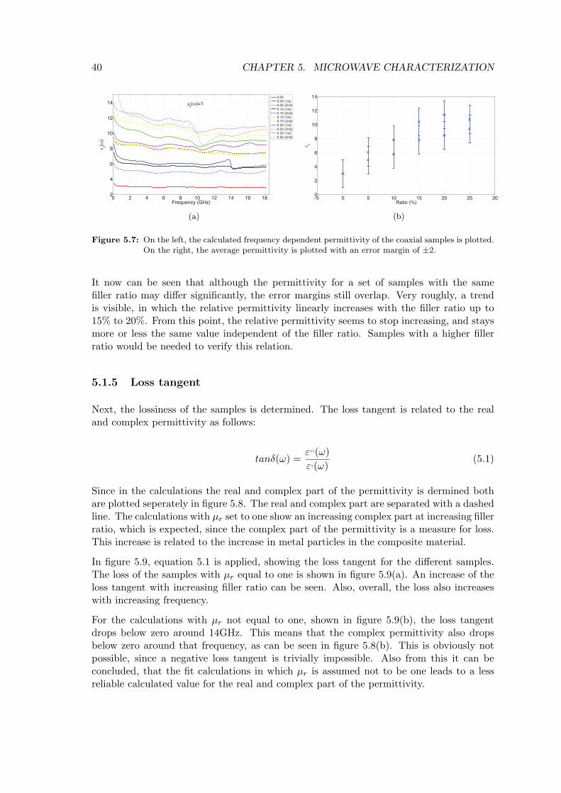
40 CHAPTER 5. MICROWAVE CHARACTERIZATION
0 2 4 6 8 10 12 14 16 182
4
6
8
10
12
14
Frequency (GHz)
ε r(ω)
0.000.05 (1st)0.05 (2nd)0.10 (1st)0.10 (2nd)0.15 (1st)0.15 (2nd)0.20 (1st)0.20 (2nd)0.25 (1st)0.25 (2nd)
μr(ω)=1
(a)
−5 0 5 10 15 20 25 300
2
4
6
8
10
12
14
Ratio (%)
ε r
(b)
Figure 5.7: On the left, the calculated frequency dependent permittivity of the coaxial samples is plotted.On the right, the average permittivity is plotted with an error margin of ±2.
It now can be seen that although the permittivity for a set of samples with the samefiller ratio may differ significantly, the error margins still overlap. Very roughly, a trendis visible, in which the relative permittivity linearly increases with the filler ratio up to15% to 20%. From this point, the relative permittivity seems to stop increasing, and staysmore or less the same value independent of the filler ratio. Samples with a higher fillerratio would be needed to verify this relation.
5.1.5 Loss tangent
Next, the lossiness of the samples is determined. The loss tangent is related to the realand complex permittivity as follows:
tanδ(ω) =ε,,(ω)ε,(ω)
(5.1)
Since in the calculations the real and complex part of the permittivity is dermined bothare plotted seperately in figure 5.8. The real and complex part are separated with a dashedline. The calculations with µr set to one show an increasing complex part at increasing fillerratio, which is expected, since the complex part of the permittivity is a measure for loss.This increase is related to the increase in metal particles in the composite material.
In figure 5.9, equation 5.1 is applied, showing the loss tangent for the different samples.The loss of the samples with µr equal to one is shown in figure 5.9(a). An increase of theloss tangent with increasing filler ratio can be seen. Also, overall, the loss also increaseswith increasing frequency.
For the calculations with µr not equal to one, shown in figure 5.9(b), the loss tangentdrops below zero around 14GHz. This means that the complex permittivity also dropsbelow zero around that frequency, as can be seen in figure 5.8(b). This is obviously notpossible, since a negative loss tangent is trivially impossible. Also from this it can beconcluded, that the fit calculations in which µr is assumed not to be one leads to a lessreliable calculated value for the real and complex part of the permittivity.
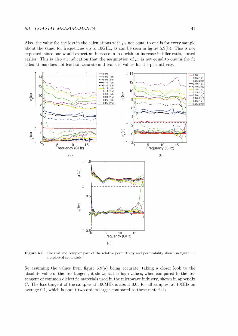
5.1. COAXIAL MEASUREMENTS 41
Also, the value for the loss in the calculations with µr not equal to one is for every sampleabout the same, for frequencies up to 10GHz, as can be seen in figure 5.9(b). This is notexpected, since one would expect an increase in loss with an increase in filler ratio, statedearlier. This is also an indication that the assumption of µr is not equal to one in the fitcalculations does not lead to accurate and realistic values for the permittivity.
0 5 10 150
2
4
6
8
10
12
14
Frequency (GHz)
0.000.05 (1st)0.05 (2nd)0.10 (1st)0.10 (2nd)0.15 (1st)0.15 (2nd)0.20 (1st)0.20 (2nd)0.25 (1st)0.25 (2nd)
ε, r(ω)
ε,, r
(ω)
(a)
0 5 10 15−2
0
2
4
6
8
10
12
14
Frequency (GHz)
0.000.05 (1st)0.05 (2nd)0.10 (1st)0.10 (2nd)0.15 (1st)0.15 (2nd)0.20 (1st)0.20 (2nd)0.25 (1st)0.25 (2nd)
ε, r(ω)
ε,, r(ω)
(b)
0 5 10 15−0.5
0
0.5
1
1.5
Frequency (GHz)
, r(ω)
,, r(ω)
μμ
(c)
Figure 5.8: The real and complex part of the relative permittivity and permeability shown in figure 5.5are plotted separately.
So assuming the values from figure 5.9(a) being accurate, taking a closer look to theabsolute value of the loss tangent, it shows rather high values, when compared to the losstangent of common dielectric materials used in the microwave industry, shown in appendixC. The loss tangent of the samples at 100MHz is about 0.05 for all samples, at 10GHz onaverage 0.1, which is about two orders larger compared to these materials.

42 CHAPTER 5. MICROWAVE CHARACTERIZATION
0 5 10 150
0.05
0.1
0.15
0.2
0.25
0.3
0.35
0.4
Frequency (GHz)
tanδ (ω
)
0.000.05 (1st)0.05 (2nd)0.10 (1st)0.10 (2nd)0.15 (1st)0.15 (2nd)0.20 (1st)0.20 (2nd)0.25 (1st)0.25 (2nd)
μr(ω)=1
(a)
0 5 10 15−0.2
−0.1
0
0.1
0.2
0.3
0.4
0.5
Frequency (GHz)
tanδ (ω
)
0.00
0.05 (1st)0.05 (2nd)0.10 (1st)
0.10 (2nd)0.15 (1st)0.15 (2nd)
0.20 (1st)0.20 (2nd)0.25 (1st)
0.25 (2nd)
μr(ω)"1
(b)
Figure 5.9: The loss tangent of each sample. The calculation with µr set to one, shown in figure 5.9(a),shows a clear relation between the lossiness and the filler ratio, were tanδ increases withincreasing filler ratio. The strange rise in the 25% sample for low frequencies is clearly anartifact related to the steep rise in the complex part of the permittivity, the rise in relativepermittivity shown in figure 5.5(a) and the non-zero transmission at low frequency shown infigure 5.3, discussed in the previous section. It is not a result of an intrinsic property of thissample, as no other sample shows this behaviour.
5.1.6 Conclusions coax measurements
In a coaxial network analyzer setup, a series of samples with varying silver particle fillerratio is analyzed. These measurements produce a scatter matrix, which gives informationabout the reflection and transmission behaviour of the samples.
The frequency depending scatter matrix showed a clear filler ratio dependence of trans-mission and reflection. With increasing filler ratio, reflection increased and transmissiondecreased. The samples with the highest filler ratio, 20% and 25%, showed strange be-haviour, as they showed contradictory behaviour with a lower transmission for the 20%sample. This is very likely to be caused by imperfect dimensions of the sample. Thisis verified when the samples dimensions were measured. The 25% samples showed lessperfect fit, which leads to leakage.
Next, from the scatter matrix measurements, the frequency dependent real and complexpart of the permittivity and permeability can be determined. Two types of calculations arecarried out, with and without the permeability taken into account. When the permeabilityis taken into account, the fit led to negative values for the complex permittivity and hence,the loss tangent. Since this is impossible, the calculations with the magnetization, ora permeability fixed to one, led to more credible values for the permittivity. This alsomeans that no significant magnetization occurs in the material as expected, since silver isdiamagnetic with a permeability close to one.
Irregularities are present in the scatter matrix measurements, and therefore permittivitycalculations, which are likely to be caused by inhomogenities such as the silver particles notbeing spread homogeneous on microscopic scale. Macroscopically, there were air bubblespresent in the samples, but very likely do not contribute to these irregularities.

5.1. COAXIAL MEASUREMENTS 43
Also, values for the permittivity of samples with equal filler ratio were significantly devi-ating. It has been shown that dimensional misfit of the samples in the sample holder hasa significant influence on the calculated value for the permittivity.
For the permittivity calculations, a rough error margin estimation has been carried out. Itis concluded that the dimensions of the sample as input parameters for the calculations areof most significant influence on the permittivity. Roughly, the permittivity calculationshave an error of about ±2. This is an average, samples with lower filler ratio have a smallererror, with a higher filler ratio a higher error.
A closer look on the average relative permittivity with the error margins taken in account,a clear qualitative relation between the filler ratio and the permittivity can be seen, whichincreases with increasing filler ratio. Also, the permittivity seems to increase linearly withincreasing filler ratio, up to in between 15% and 20%. At higher filler ratio, the permittivityseems to become more or less independent of the filler ratio.
Also, a rough relation between the filler ratio and the lossiness of the samples is present.The loss of the composite increases with increasing filler ratio and is quantitatively verylossy compared to other commonly used materials in the microwave industry.

44 CHAPTER 5. MICROWAVE CHARACTERIZATION
5.2 Low power X-band measurements
In the previous section, the material properties of the used composite material are deter-mined. This section will outline microwave measurements in an X-band waveguide setupon samples made from the same composite material. The measurements have been carriedout, to see how these composites with different filler ratios react in an actual waveguidesetup. The microwave X-band covers a frequency span of 8GHz to 12GHz, much smallerthan the previous measurements, which were carried out in a span of 100MHz to 18.2GHz.In a network analyzer setup the scatter matrix of various samples is measured over theX-band frequency width.
In the previous section, a software fitting algorithm was used to calculate the relativedielectric constant and permeability of the samples from the scatter matrix data. In thissection, a fit is carried using a matlab algorithm, which models an X-band setup. Forvarious input parameters such as the permittivity and the permeability, a scatter matrix iscalculated mathematically. This will be outlined more thoroughly later on. By adjustingthe initial input parameters of the model such that the calculated scatter matrix fits themeasurements, the material parameters are determined and compared to the calculatedvalues in the previous section.
This section first will outline the construction of the various samples to fit an X-bandwaveguide.This chapter will outline on the sample preparation and the results of the RFmeasurements.
5.2.1 Sample preparation and experimental setup
To carry out the X-band waveguide measurements, samples with accurate waveguide di-mensions need to be constructed. This to prevent leakage on the sides of the sample insidethe waveguide. Therefore a mold is constructed. By lasercutting the exact sized holes arecut in the sample holder. The size for X-band measurements is 22.86 x 10.16mm.
Figure 5.10: Schematic representation of the mold used for constructing the X-band measurement sam-ples.
The holes are subsequently filled with the composite material with different volume ratios
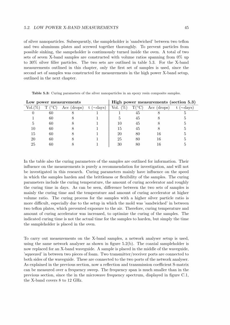
5.2. LOW POWER X-BAND MEASUREMENTS 45
of silver nanoparticles. Subsequently, the sampleholder is ’sandwiched’ between two teflonand two aluminum plates and screwed together thoroughly. To prevent particles frompossible sinking, the sampeholder is continuously turned inside the oven. A total of twosets of seven X-band samples are constructed with volume ratios spanning from 0% upto 30% silver filler particles. The two sets are outlined in table 5.3. For the X-bandmeasurements outlined in this chapter, only the first set of samples is used, since thesecond set of samples was constructed for measurements in the high power X-band setup,outlined in the next chapter.
Table 5.3: Curing parameters of the silver nanoparticles in an epoxy resin composite samples.
Low power measurements High power measurements (section 5.3)Vol.(%) T (C) Acc (drops) t (∼days) Vol. (%) T(C) Acc (drops) t (∼days)
0 60 8 1 1 45 8 51 60 8 1 5 45 8 55 60 8 1 10 45 8 510 60 8 1 15 45 8 515 60 8 1 20 80 16 520 60 8 1 25 80 16 525 60 8 1 30 80 16 5
In the table also the curing parameters of the samples are outlined for information. Theirinfluence on the measurements is purely a recommendation for investigation, and will notbe investigated in this research. Curing parameters mainly have influence on the speedin which the samples harden and the brittleness or flexibility of the samples. The curingparameters include the curing temperature, the amount of curing accelerator and roughlythe curing time in days. As can be seen, difference between the two sets of samples ismainly the curing time and the temperature and amount of curing accelerator at highervolume ratio. The curing process for the samples with a higher silver particle ratio ismore difficult, especially due to the setup in which the mold was ’sandwiched’ in betweentwo teflon plates, which prevented exposure to the air. Therefore, curing temperature andamount of curing accelerator was increased, to optimize the curing of the samples. Theindicated curing time is not the actual time for the samples to harden, but simply the timethe sampleholder is placed in the oven.
To carry out measurements on the X-band samples, a network analyser setup is used,using the same network analyser as shown in figure 5.2(b). The coaxial sampleholder isnow replaced for an X-band waveguide. A sample is placed in the middle of the waveguide,’squeezed’ in between two pieces of foam. Two transmitter/receiver ports are connected toboth sides of the waveguide. These are connected to the two ports of the network analyser.As explained in the previous section, now a reflection and transmission coefficient S-matrixcan be measured over a frequency sweep. The frequency span is much smaller than in theprevious section, since the in the microwave frequency spectrum, displayed in figure C.1,the X-band covers 8 to 12 GHz.
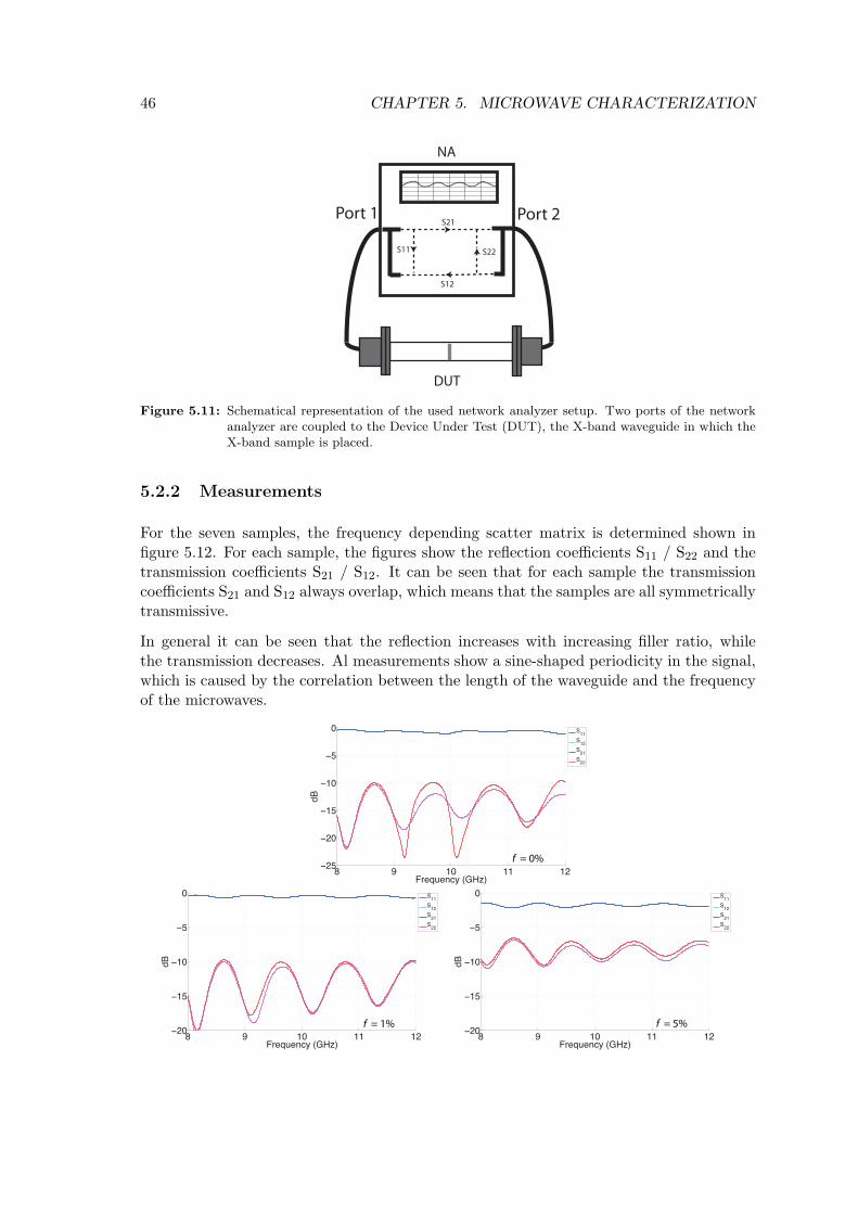
46 CHAPTER 5. MICROWAVE CHARACTERIZATION
Port 1 Port 2
S11 S22
S21
S12
DUT
NA
Figure 5.11: Schematical representation of the used network analyzer setup. Two ports of the networkanalyzer are coupled to the Device Under Test (DUT), the X-band waveguide in which theX-band sample is placed.
5.2.2 Measurements
For the seven samples, the frequency depending scatter matrix is determined shown infigure 5.12. For each sample, the figures show the reflection coefficients S11 / S22 and thetransmission coefficients S21 / S12. It can be seen that for each sample the transmissioncoefficients S21 and S12 always overlap, which means that the samples are all symmetricallytransmissive.
In general it can be seen that the reflection increases with increasing filler ratio, whilethe transmission decreases. Al measurements show a sine-shaped periodicity in the signal,which is caused by the correlation between the length of the waveguide and the frequencyof the microwaves.
8 9 10 11 12−25
−20
−15
−10
−5
0
Frequency (GHz)
dB
S11
S12
S21
S22
f = 0%
8 9 10 11 12−20
−15
−10
−5
0
Frequency (GHz)
dB
S11
S12
S21
S22
f = 1%
8 9 10 11 12−20
−15
−10
−5
0
Frequency (GHz)
dB
S11
S12
S21
S22
f = 5%
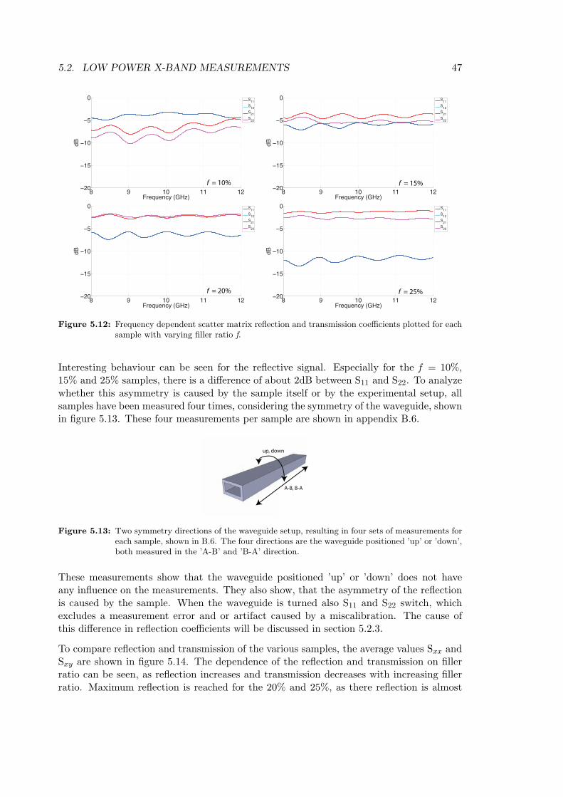
5.2. LOW POWER X-BAND MEASUREMENTS 47
8 9 10 11 12−20
−15
−10
−5
0
Frequency (GHz)
dB
S11
S12
S21
S22
f = 10%
8 9 10 11 12−20
−15
−10
−5
0
Frequency (GHz)
dB
S11
S12
S21
S22
f = 15%
8 9 10 11 12−20
−15
−10
−5
0
Frequency (GHz)
dB
S11
S12
S21
S22
f = 20%
8 9 10 11 12−20
−15
−10
−5
0
Frequency (GHz)
dB
S11
S12
S21
S22
f = 25%
Figure 5.12: Frequency dependent scatter matrix reflection and transmission coefficients plotted for eachsample with varying filler ratio f.
Interesting behaviour can be seen for the reflective signal. Especially for the f = 10%,15% and 25% samples, there is a difference of about 2dB between S11 and S22. To analyzewhether this asymmetry is caused by the sample itself or by the experimental setup, allsamples have been measured four times, considering the symmetry of the waveguide, shownin figure 5.13. These four measurements per sample are shown in appendix B.6.
A-B, B-A
up, down
Figure 5.13: Two symmetry directions of the waveguide setup, resulting in four sets of measurements foreach sample, shown in B.6. The four directions are the waveguide positioned ’up’ or ’down’,both measured in the ’A-B’ and ’B-A’ direction.
These measurements show that the waveguide positioned ’up’ or ’down’ does not haveany influence on the measurements. They also show, that the asymmetry of the reflectionis caused by the sample. When the waveguide is turned also S11 and S22 switch, whichexcludes a measurement error and or artifact caused by a miscalibration. The cause ofthis difference in reflection coefficients will be discussed in section 5.2.3.
To compare reflection and transmission of the various samples, the average values Sxx andSxy are shown in figure 5.14. The dependence of the reflection and transmission on fillerratio can be seen, as reflection increases and transmission decreases with increasing fillerratio. Maximum reflection is reached for the 20% and 25%, as there reflection is almost
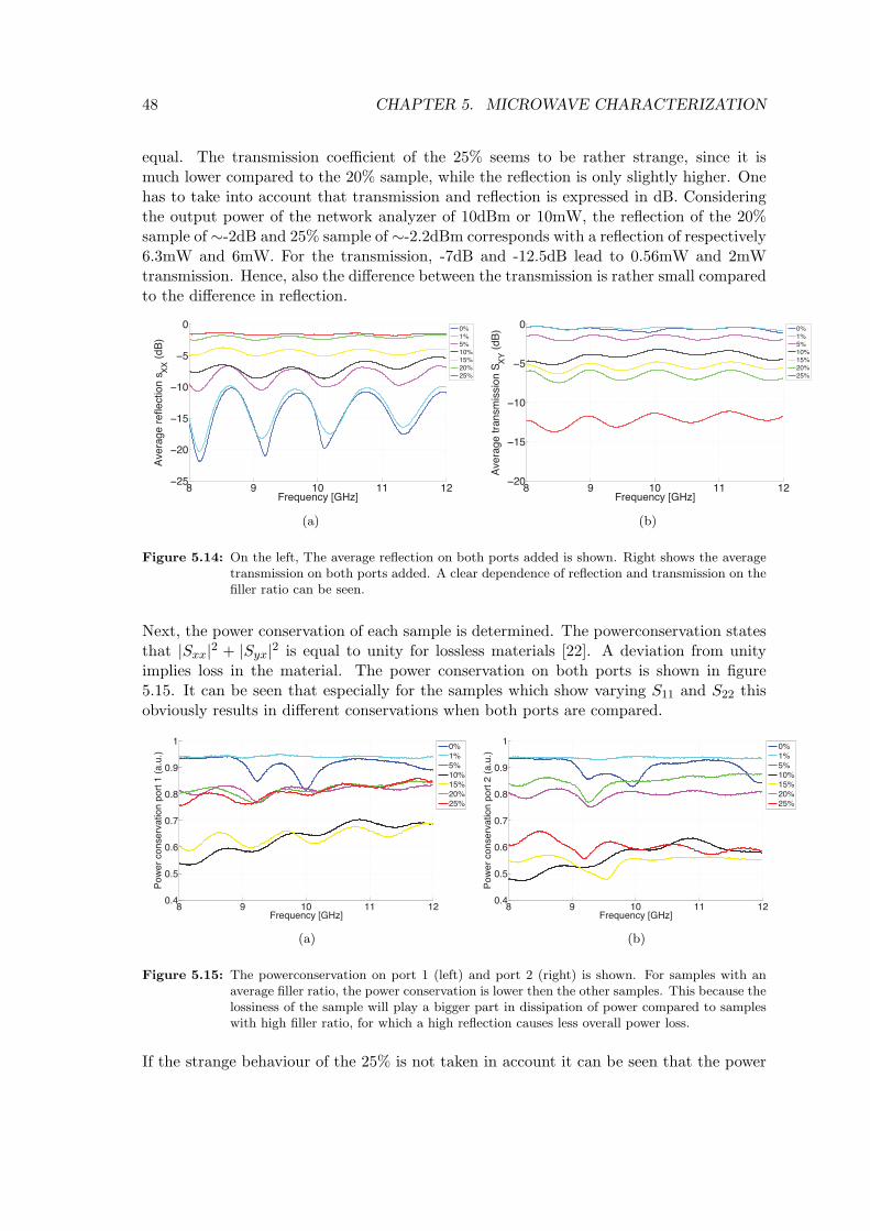
48 CHAPTER 5. MICROWAVE CHARACTERIZATION
equal. The transmission coefficient of the 25% seems to be rather strange, since it ismuch lower compared to the 20% sample, while the reflection is only slightly higher. Onehas to take into account that transmission and reflection is expressed in dB. Consideringthe output power of the network analyzer of 10dBm or 10mW, the reflection of the 20%sample of ∼-2dB and 25% sample of ∼-2.2dBm corresponds with a reflection of respectively6.3mW and 6mW. For the transmission, -7dB and -12.5dB lead to 0.56mW and 2mWtransmission. Hence, also the difference between the transmission is rather small comparedto the difference in reflection.
8 9 10 11 12−25
−20
−15
−10
−5
0
Frequency [GHz]
Average reflection sXX (dB)
0%1%5%10%15%20%25%
(a)
8 9 10 11 12−20
−15
−10
−5
0
Frequency [GHz]Average transmission SXY (dB)
0%1%5%10%15%20%25%
(b)
Figure 5.14: On the left, The average reflection on both ports added is shown. Right shows the averagetransmission on both ports added. A clear dependence of reflection and transmission on thefiller ratio can be seen.
Next, the power conservation of each sample is determined. The powerconservation statesthat |Sxx|2 + |Syx|2 is equal to unity for lossless materials [22]. A deviation from unityimplies loss in the material. The power conservation on both ports is shown in figure5.15. It can be seen that especially for the samples which show varying S11 and S22 thisobviously results in different conservations when both ports are compared.
8 9 10 11 120.4
0.5
0.6
0.7
0.8
0.9
1
Frequency [GHz]
Po
we
r co
nse
rva
tio
n p
ort
1 (
a.u
.)
0%1%5%10%15%20%25%
(a)
8 9 10 11 120.4
0.5
0.6
0.7
0.8
0.9
1
Frequency [GHz]
Po
we
r co
nse
rva
tio
n p
ort
2 (
a.u
.)
0%1%5%10%15%20%25%
(b)
Figure 5.15: The powerconservation on port 1 (left) and port 2 (right) is shown. For samples with anaverage filler ratio, the power conservation is lower then the other samples. This because thelossiness of the sample will play a bigger part in dissipation of power compared to sampleswith high filler ratio, for which a high reflection causes less overall power loss.
If the strange behaviour of the 25% is not taken in account it can be seen that the power

5.2. LOW POWER X-BAND MEASUREMENTS 49
conservation for the 0% and 1% is closest to unity, followed by the 5% and 20% sampleswith a conservation of about 80%. The 10% and 15% samples show power conservationof about 60%. This does not immediately mean that these samples are the most lossy.Considering the following. The samples with low filler ratio are less lossy and highlytransmissive, which results in a powerconservation close to unity. For a sample with highfiller ratio, which has a high reflection coefficient, almost all energy is reflected, only avery small amount of power transmits or ’penetrates’ in the material and is subjected tothe lossiness of the material. Therefore, also for samples with a high filler ratio, the powerconservation is close to unity.
But for the samples with a filler ratio in between these extremes the amount of transmittedpower is significantly subjected to the possible lossiness of the material, which results in apower conservation deviating from unity.
The fact that the power conservation for the 10% and 15% samples is significantly deviatingfrom unity, it can be concluded that the composite material indeed is lossy, which matchescoaxial measurements and calculations. Again, the fact that the power conservation ofthe 20% and 25% samples is closer to unity does not mean that the composite materialat these ratios is not lossy anymore. Simply due to the higher reflective behaviour of thecomposite at these ratios, less power is transmitted and subjected to the lossiness of thematerial, resulting in a power conservation closer to unity. This limits in for instance apiece of metal perfectly fitting in the waveguide were |Sxx| is unity and |Syx| zero, resultingin a power conservation equal to unity.
5.2.3 Theoretical waveguide model fit to measurements
To determine material parameters from the scatter matrix data Thales developed a codefor calculating the scatter matrix for a waveguide setup with certain dimensions and alayer composition inside the waveguide with certain material parameters. The parametersfor this fitmodel are outlined in table 5.4.
Table 5.4: Input parameters for the X-band waveguide model developed by Thales to calculate the re-flection and transmission scatter matrix of an X-band waveguide setup.
Parameters fitmodel ValuesWaveguide dimensions BxH (mm) 22.86mm x 10.16mmFrequency (GHz) 8-12GHz, 26 pointsLayer composition layers (mm)Relative permittivity per layer (εr) (εr) per layerLoss tangent per layer (tanδ) (tanδ) per layerRelative permeability per layer(µr) (µr) per layer
Non coinciding S11 and S22 coefficients due to varying loss
In the previous section the scatter matrix measurements were discussed, were some samplesshowed non coinciding reflection coefficients. Calculations have shown that a waveguide

50 CHAPTER 5. MICROWAVE CHARACTERIZATION
setup filled with various layers with varying material parameters will have different S11
and S22 reflection coefficients. It has shown that mostly a difference in lossiness of thelayers is the main cause of this non coinciding. But obviously, in the case of the usedcomposite, a higher loss indicates a higher filler ratio of silver particles, which also leadsto a higher dielectric value of this layer.
An example of non coinciding reflection parameters caused by layers with varying loss coef-ficients is given below. In the example the setup that has been used for the measurementsis modelled. This includes the waveguide setup with the dimensions mentioned in table5.4. Length of the waveguide is 206mm. Inside the waveguide a sample with a thickness of1mm is placed, ’squeezed’ in between two pieces of foam. The permittivity εr of the foamis 1.08, the loss tangent tanδ of the foam is 0.0025, negligible compared to the loss of thesample. The 1mm thick sample is modelled as two layers with a thickness of 0.5mm.
Two situations are modelled. In both cases the permittivity εr is assumed to be 4. Inthe first case, the loss tangent tanδ of both layers is 0.01, in the second case, the losstangent of the first layer is 0.01, the second layer is much higher, 0.5. Again, these valuesdo not represent a realistic setup, since a layer with a higher loss will also have a higherpermittivity, but these values are chosen to show the influence of a diference in only theloss of the two layers. Figure 5.16 shows a schematic example of this waveguidesetup filledwith two layers of dielectric material between two pieces of foam. The model assumes aperfect fit of the layer material without any leakage.
Waveguide side view
Port 1 Port 2
Waveguide front view
H
B
ε =4r
μ =1r
tanδ= 0.01
1mm
ε =1.08rμ =1r
tanδ= 0.0025
FoamFoam
ε =4r
μ =1r
tanδ= 0.01/0.5
1st layer 2nd layer
Figure 5.16: Schematical representation of the X-band waveguide setup, in which the 1mm thick com-posite sample is modeled as two layers, which equal and different loss tangent.
The calculation results of the two situations are shown in figure 5.17. Figure 5.17(a) showsthe situation in which both layers have the same loss tangent, which means that the twolayers in fact form one dielectric layer with a thickness of 1mm. As expected the tworeflection and transmission coefficients coincide. Figure 5.17(b) shows the calculations inthe second situation, in which both layers vary in loss, respectivily 0.01 and 0.5. It can beseen that the transmission coefficients overlap, but there is a small difference in reflectioncoefficients. Similarities can be seen when these results are compared with the X-bandmeasurements shown in figure 5.12.
The position of the sample could also obviously influence this discrepancy. This is alsoinvestigated with the model. It showed that since the sample is very thin (1mm) compared
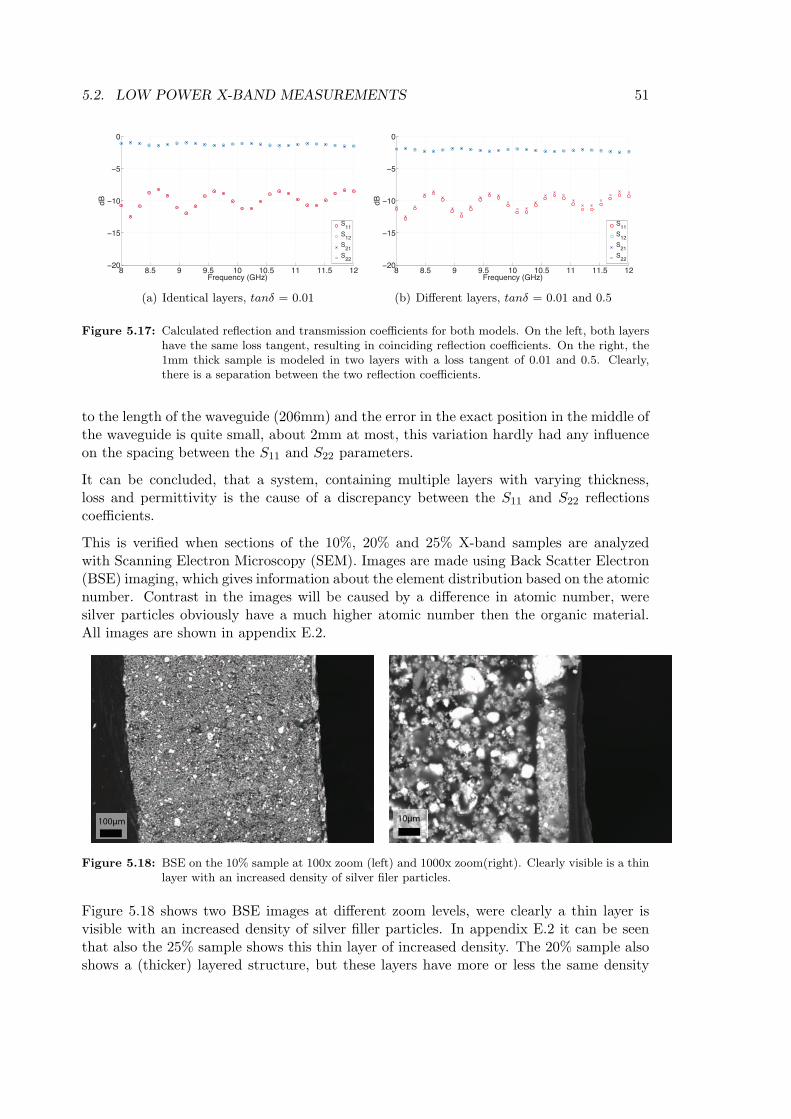
5.2. LOW POWER X-BAND MEASUREMENTS 51
8 8.5 9 9.5 10 10.5 11 11.5 12−20
−15
−10
−5
0
Frequency (GHz)
dB
S11
S12
S21
S22
(a) Identical layers, tanδ = 0.01
8 8.5 9 9.5 10 10.5 11 11.5 12−20
−15
−10
−5
0
Frequency (GHz)
dB
S11
S12
S21
S22
(b) Different layers, tanδ = 0.01 and 0.5
Figure 5.17: Calculated reflection and transmission coefficients for both models. On the left, both layershave the same loss tangent, resulting in coinciding reflection coefficients. On the right, the1mm thick sample is modeled in two layers with a loss tangent of 0.01 and 0.5. Clearly,there is a separation between the two reflection coefficients.
to the length of the waveguide (206mm) and the error in the exact position in the middle ofthe waveguide is quite small, about 2mm at most, this variation hardly had any influenceon the spacing between the S11 and S22 parameters.
It can be concluded, that a system, containing multiple layers with varying thickness,loss and permittivity is the cause of a discrepancy between the S11 and S22 reflectionscoefficients.
This is verified when sections of the 10%, 20% and 25% X-band samples are analyzedwith Scanning Electron Microscopy (SEM). Images are made using Back Scatter Electron(BSE) imaging, which gives information about the element distribution based on the atomicnumber. Contrast in the images will be caused by a difference in atomic number, weresilver particles obviously have a much higher atomic number then the organic material.All images are shown in appendix E.2.
100μm 10μm
Figure 5.18: BSE on the 10% sample at 100x zoom (left) and 1000x zoom(right). Clearly visible is a thinlayer with an increased density of silver filer particles.
Figure 5.18 shows two BSE images at different zoom levels, were clearly a thin layer isvisible with an increased density of silver filler particles. In appendix E.2 it can be seenthat also the 25% sample shows this thin layer of increased density. The 20% sample alsoshows a (thicker) layered structure, but these layers have more or less the same density
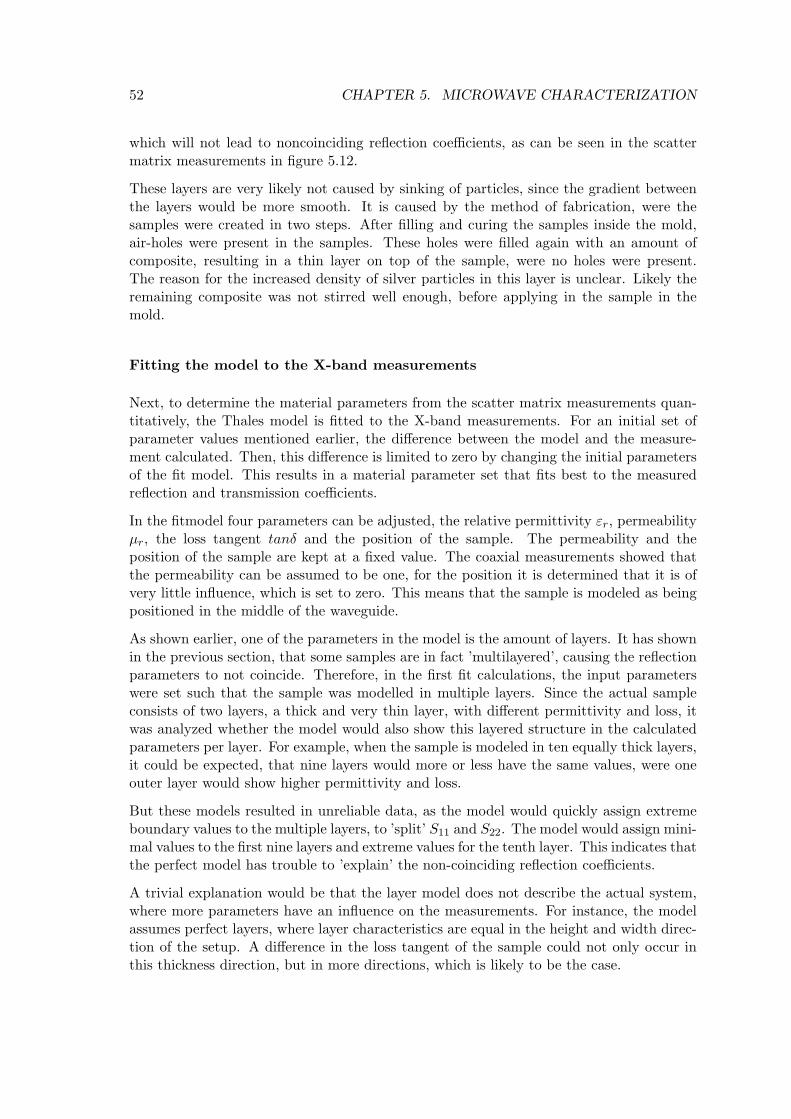
52 CHAPTER 5. MICROWAVE CHARACTERIZATION
which will not lead to noncoinciding reflection coefficients, as can be seen in the scattermatrix measurements in figure 5.12.
These layers are very likely not caused by sinking of particles, since the gradient betweenthe layers would be more smooth. It is caused by the method of fabrication, were thesamples were created in two steps. After filling and curing the samples inside the mold,air-holes were present in the samples. These holes were filled again with an amount ofcomposite, resulting in a thin layer on top of the sample, were no holes were present.The reason for the increased density of silver particles in this layer is unclear. Likely theremaining composite was not stirred well enough, before applying in the sample in themold.
Fitting the model to the X-band measurements
Next, to determine the material parameters from the scatter matrix measurements quan-titatively, the Thales model is fitted to the X-band measurements. For an initial set ofparameter values mentioned earlier, the difference between the model and the measure-ment calculated. Then, this difference is limited to zero by changing the initial parametersof the fit model. This results in a material parameter set that fits best to the measuredreflection and transmission coefficients.
In the fitmodel four parameters can be adjusted, the relative permittivity εr, permeabilityµr, the loss tangent tanδ and the position of the sample. The permeability and theposition of the sample are kept at a fixed value. The coaxial measurements showed thatthe permeability can be assumed to be one, for the position it is determined that it is ofvery little influence, which is set to zero. This means that the sample is modeled as beingpositioned in the middle of the waveguide.
As shown earlier, one of the parameters in the model is the amount of layers. It has shownin the previous section, that some samples are in fact ’multilayered’, causing the reflectionparameters to not coincide. Therefore, in the first fit calculations, the input parameterswere set such that the sample was modelled in multiple layers. Since the actual sampleconsists of two layers, a thick and very thin layer, with different permittivity and loss, itwas analyzed whether the model would also show this layered structure in the calculatedparameters per layer. For example, when the sample is modeled in ten equally thick layers,it could be expected, that nine layers would more or less have the same values, were oneouter layer would show higher permittivity and loss.
But these models resulted in unreliable data, as the model would quickly assign extremeboundary values to the multiple layers, to ’split’ S11 and S22. The model would assign mini-mal values to the first nine layers and extreme values for the tenth layer. This indicates thatthe perfect model has trouble to ’explain’ the non-coinciding reflection coefficients.
A trivial explanation would be that the layer model does not describe the actual system,where more parameters have an influence on the measurements. For instance, the modelassumes perfect layers, where layer characteristics are equal in the height and width direc-tion of the setup. A difference in the loss tangent of the sample could not only occur inthis thickness direction, but in more directions, which is likely to be the case.

5.2. LOW POWER X-BAND MEASUREMENTS 53
Therefore the waveguide setup is modeled more simply as just one layer in between foam,which results in more plausible calculated values. The fits to the measured reflection andtransmission coefficients per sample are shown in figure 5.19.
Since the setup is modeled with a one layer sample between two pieces of foam in a fixedposition, S11 and S22 calculated by the model obviously coincide, as explained earlier.Therefore, the model is fitted to the sum of the measured S11 and S22, which will lead toan average fit in between the S11 and S22 measurements.
8 9 10 11 12−25
−20
−15
−10
−5
0
Frequency (GHz)
dB
S11
S12
S21
S22
S11/22
fit
S12/21
fit
f = 0%
8 9 10 11 12−25
−20
−15
−10
−5
0
Frequency (GHz)
dB
S11
S12
S21
S22
S11/22
fit
S12/21
fit
f = 1%
8 9 10 11 12−25
−20
−15
−10
−5
0
Frequency (GHz)
dB
S11
S12
S21
S22
S11/22
fit
S12/21
fit
f = 5%
8 9 10 11 12−25
−20
−15
−10
−5
0
Frequency (GHz)
dB
S11
S12
S21
S22
S11/22
fit
S12/21
fit
f = 10%
8 9 10 11 12−25
−20
−15
−10
−5
0
Frequency (GHz)
dB
S11
S12
S21
S22
S11/22
fit
S12/21
fit
f = 15%
8 9 10 11 12−25
−20
−15
−10
−5
0
Frequency (GHz)
dB
S11
S12
S21
S22
S11/22
fit
S12/21
fit
f = 20%
8 9 10 11 12−25
−20
−15
−10
−5
0
Frequency (GHz)
dB
S11
S12
S21
S22
S11/22
fit
S12/21
fit
f = 25%
Figure 5.19: The reflection and transmission coefficients per sample as shown in figure 5.12. Indicatedwith × and are the fit calculations to the average of respectively the S11 and S22 reflectionand S21 and S12 transmission of each sample.
It can be seen that the calculations especially for the higher filler ratio fit the measurements
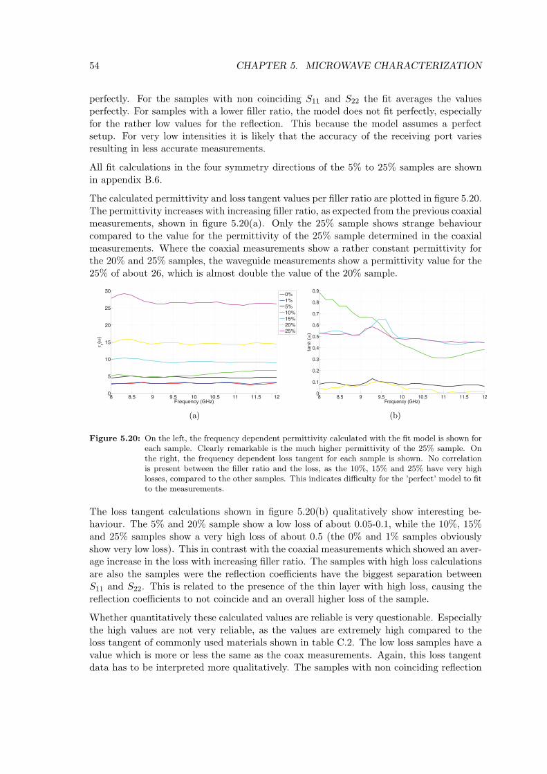
54 CHAPTER 5. MICROWAVE CHARACTERIZATION
perfectly. For the samples with non coinciding S11 and S22 the fit averages the valuesperfectly. For samples with a lower filler ratio, the model does not fit perfectly, especiallyfor the rather low values for the reflection. This because the model assumes a perfectsetup. For very low intensities it is likely that the accuracy of the receiving port variesresulting in less accurate measurements.
All fit calculations in the four symmetry directions of the 5% to 25% samples are shownin appendix B.6.
The calculated permittivity and loss tangent values per filler ratio are plotted in figure 5.20.The permittivity increases with increasing filler ratio, as expected from the previous coaxialmeasurements, shown in figure 5.20(a). Only the 25% sample shows strange behaviourcompared to the value for the permittivity of the 25% sample determined in the coaxialmeasurements. Where the coaxial measurements show a rather constant permittivity forthe 20% and 25% samples, the waveguide measurements show a permittivity value for the25% of about 26, which is almost double the value of the 20% sample.
8 8.5 9 9.5 10 10.5 11 11.5 120
5
10
15
20
25
30
Frequency (GHz)
ε r(ω)
0%
1%
5%
10%
15%
20%
25%
(a)
8 8.5 9 9.5 10 10.5 11 11.5 120
0.1
0.2
0.3
0.4
0.5
0.6
0.7
0.8
0.9
Frequency (GHz)
tanδ (ω
)
(b)
Figure 5.20: On the left, the frequency dependent permittivity calculated with the fit model is shown foreach sample. Clearly remarkable is the much higher permittivity of the 25% sample. Onthe right, the frequency dependent loss tangent for each sample is shown. No correlationis present between the filler ratio and the loss, as the 10%, 15% and 25% have very highlosses, compared to the other samples. This indicates difficulty for the ’perfect’ model to fitto the measurements.
The loss tangent calculations shown in figure 5.20(b) qualitatively show interesting be-haviour. The 5% and 20% sample show a low loss of about 0.05-0.1, while the 10%, 15%and 25% samples show a very high loss of about 0.5 (the 0% and 1% samples obviouslyshow very low loss). This in contrast with the coaxial measurements which showed an aver-age increase in the loss with increasing filler ratio. The samples with high loss calculationsare also the samples were the reflection coefficients have the biggest separation betweenS11 and S22. This is related to the presence of the thin layer with high loss, causing thereflection coefficients to not coincide and an overall higher loss of the sample.
Whether quantitatively these calculated values are reliable is very questionable. Especiallythe high values are not very reliable, as the values are extremely high compared to theloss tangent of commonly used materials shown in table C.2. The low loss samples have avalue which is more or less the same as the coax measurements. Again, this loss tangentdata has to be interpreted more qualitatively. The samples with non coinciding reflection

5.2. LOW POWER X-BAND MEASUREMENTS 55
parameters have a highly lossy thin layer, measured with SEM, which in the fit modelleads to a high overall loss The average reflection, to which is fitted, is lower, resulting inthe model to a higher loss.
Since the permittivity more or less has an constant value, as can be seen in figure 5.20(a),the average value is plotted together with the average permittivity values from the coaxialmeasurements for comparison, both shown in figure 5.21. It can be seen that for lowerfiller ratio, the measurements perfectly fit the coaxial measurements. Only the 25% sampledoes not match with the coaxial measurement.
−5 0 5 10 15 20 25 300
5
10
15
20
25
30
Ratio (%)
ε r
= X-band setup
= Coaxial setup
Figure 5.21: The average permittivity plotted against the filler ratio for both the coaxial as the x-bandmeasurements. An overlap is clearly visible for the lower filler ratio.
5.2.4 Conclusions low power X-band measurements
In an X-band network analyser setup RF microwave measurements have been carried outon a set of samples made from the composite material containing varying ratio’s of silverparticles embedded in an epoxy resin. Standard two-port scatter matrix data was obtainedcontaining reflection parameters S11 and S22 and transmission coefficients S21 and S12,measured in four directions. Overall an increase in reflectivity and decrease in transmissionwith increasing filler ratio was observed. Three samples showed strange behaviour, as thereflection coefficients do not coincide, inherent to the sample. Furthermore, transmissionin the highest filler ratio sample was deviating from the average decreasing trend in thetransmission.
A waveguide model has been developed by Thales to calculate theoretically the scatter-matrix coefficients depending on waveguide dimensions, frequency span, layer compositioninside the waveguide, thickness, permittivity, permeability and loss tangent of each layer.It is shown, that the main cause for non coinciding reflection coefficients is a differencein loss tangent of various layers. This would indicate that the sample lacks homogeneityin the thickness direction. This is verified by SEM images of section of the samples. The
56 CHAPTER 5. MICROWAVE CHARACTERIZATION
samples with noncoinciding reflection coefficients showed a ∼10µm thin layer on the sideof the sample with an increased density of filler particles, very likely to be caused by thefabrication method.
The theoretical model is used to determine the permittivity and loss tangent of the varioussamples by fitting the model to the measurements. The model assumes a 1mm layer inbetween two pieces of foam with a fixed permeability of one, concluded from the coaxialmeasurements. The resulting permittivity more or less agreed the coaxial measurementsexcept for the 25% sample. The value for the loss tangent of the samples with non coincid-ing reflection parameters is very high and not very plausible, but is a qualitative indicationand verification that an extra very loss layer is present, which causes the overall loss toincrease. Values for the loss for the samples with coinciding reflection coefficients matchthe values in from the coaxial measurements.
It was attempted to model the 1mm thick samples in multiple layers, since again, thesemultiple layers are physically present, but this led to extreme and non-plausible outputvalues, which shows the difficulty for the ’perfect’ model to assign values in a less perfectsystem. Also, the model is based on a minimization between a waveguide model andthe measurements. Including more parameters introduces more possible local minima.More research on initial parameter values would be necessary to determine whether thismultilayer extensive model can actually be applied on such a system.

5.3. HIGH POWER X-BAND MEASUREMENTS 57
5.3 High power X-band measurements
All the previous microwave measurements on the composite material samples have beencarried out at constant ’low’ output power of 10dBm, or 10mW. One of the main researchgoals is to examine the power dependence of the reflective behaviour of these compositematerials. Therefore, a setup is constructed in which the X-band waveguide setup describedabove is used, in which it is possible to measure the reflectivity of the composite materialsamples inside the waveguide in a range of output power.
This section will outline these measurements. Different from the previous measurements,instead of a two-port scatter matrix, only the reflective behaviour of the X-band samples ismeasured. First, the experimental setup and the samples used is outlined in sections 5.3.1and 5.3.2. Next, the measurements and results will be outlined in sections 5.3.3, 5.3.4 and5.3.5. Last, the measurements will be compared with the low power measurements fromthe previous section to lead to the conclusions, outlined in section 5.3.6.
5.3.1 Experimental setup
To carry out measurements in a high microwave power range, a different setup needs tobe constructed, as the network analyser setup produces a limited power with a maximumoutput of 25dBm or about 300mw.
LoadTWT
DUT
Load
1st DC 2nd DC
Power meter Signal generator
Load10dB Power tap
Circulator
Figure 5.22: Schematic representation of the setup used for measuring the reflectivity of samples withvarying composition at a high power range. In this setup, the power meter is connected tothe 1st DC to measure reflectivity. When connected to the 2nd DC, the transmission linepower is measured.
Therefore, a new setup is constructed, schematically shown in figure 5.22. The mostimportant part of the setup is the travelling wave tube (TWT) amplifier. This deviceamplifies any input microwave signal up to a maximum of 56dB or 400W. In the setup,this input signal is generated by a signal generator. This device is able to generate acontinuous wave (CW) or pulsed wave, at varying frequency and power. While the TWTamplifier simply amplifies this wave by a certain amount of dBm, the output power of thesignal can be controlled by the signal generator. This makes it possible to measure over arange of power controlled by the signal generator with a maximum of 56dB, the maximumoutput of the TWT.

58 CHAPTER 5. MICROWAVE CHARACTERIZATION
The signal from the TWT will first pass through a circulator. This is a three port non-reciprocal device. This means that microwave power that is entering any port is transmit-ted to the next port only. The circulator is placed in such a way, that reflected microwavepower will be led into the connected load, instead of returning back into the TWT, whichcould damage the amplifier.
Next, the microwaves pass through an X-band waveguide setup. This setup exists of twodirectional couplers (DC), placed opposite from eachother. Although this report will notgo into the theory on which this coupling mechanism is based, in short, inside a directionalcoupler, two transmission lines are constructed close together. Due to the interaction ofthe electromagnetic fields of each line, power can be coupled between the lines [1]. Inother words, a part of the power in the transmission line will be coupled to a different lineconnected to another output port.
These directional couplers make it possible to measure the power through the transmissionline in both directions. The direction coupler used in this setup, weakens the power by∼20dBm. This means that the signal measured with the power meter at the coupledport, also connected to a power tap that weakens the signal with 10dB, is always ∼30dBmlower than the actual power through the transmission line. This weakening of the signal isnecessary, since the power sensor has a measurement range up to ∼30dBm. Higher powercould damage the power sensor.
Connected to these directional couplers is the X-band waveguide which holds the X-bandsample, the socalled Device Under Test or DUT. After the DUT, a load is placed, todissipate the power that passes through the sample.
Load
DUT
1st DC
2nd DC
Powermeter Signal generator
Circulator
TWTLoad
Figure 5.23: Actual experimental high power setup.
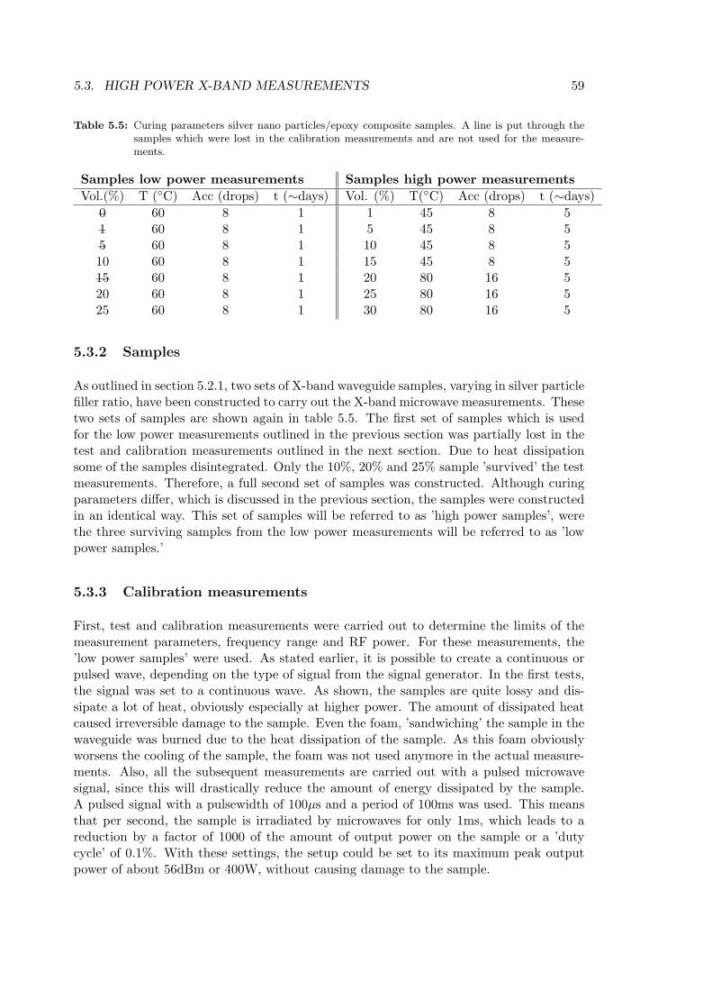
5.3. HIGH POWER X-BAND MEASUREMENTS 59
Table 5.5: Curing parameters silver nano particles/epoxy composite samples. A line is put through thesamples which were lost in the calibration measurements and are not used for the measure-ments.
Samples low power measurements Samples high power measurementsVol.(%) T (C) Acc (drops) t (∼days) Vol. (%) T(C) Acc (drops) t (∼days)
0 60 8 1 1 45 8 51 60 8 1 5 45 8 55 60 8 1 10 45 8 510 60 8 1 15 45 8 515 60 8 1 20 80 16 520 60 8 1 25 80 16 525 60 8 1 30 80 16 5
5.3.2 Samples
As outlined in section 5.2.1, two sets of X-band waveguide samples, varying in silver particlefiller ratio, have been constructed to carry out the X-band microwave measurements. Thesetwo sets of samples are shown again in table 5.5. The first set of samples which is usedfor the low power measurements outlined in the previous section was partially lost in thetest and calibration measurements outlined in the next section. Due to heat dissipationsome of the samples disintegrated. Only the 10%, 20% and 25% sample ’survived’ the testmeasurements. Therefore, a full second set of samples was constructed. Although curingparameters differ, which is discussed in the previous section, the samples were constructedin an identical way. This set of samples will be referred to as ’high power samples’, werethe three surviving samples from the low power measurements will be referred to as ’lowpower samples.’
5.3.3 Calibration measurements
First, test and calibration measurements were carried out to determine the limits of themeasurement parameters, frequency range and RF power. For these measurements, the’low power samples’ were used. As stated earlier, it is possible to create a continuous orpulsed wave, depending on the type of signal from the signal generator. In the first tests,the signal was set to a continuous wave. As shown, the samples are quite lossy and dis-sipate a lot of heat, obviously especially at higher power. The amount of dissipated heatcaused irreversible damage to the sample. Even the foam, ’sandwiching’ the sample in thewaveguide was burned due to the heat dissipation of the sample. As this foam obviouslyworsens the cooling of the sample, the foam was not used anymore in the actual measure-ments. Also, all the subsequent measurements are carried out with a pulsed microwavesignal, since this will drastically reduce the amount of energy dissipated by the sample.A pulsed signal with a pulsewidth of 100µs and a period of 100ms was used. This meansthat per second, the sample is irradiated by microwaves for only 1ms, which leads to areduction by a factor of 1000 of the amount of output power on the sample or a ’dutycycle’ of 0.1%. With these settings, the setup could be set to its maximum peak outputpower of about 56dBm or 400W, without causing damage to the sample.
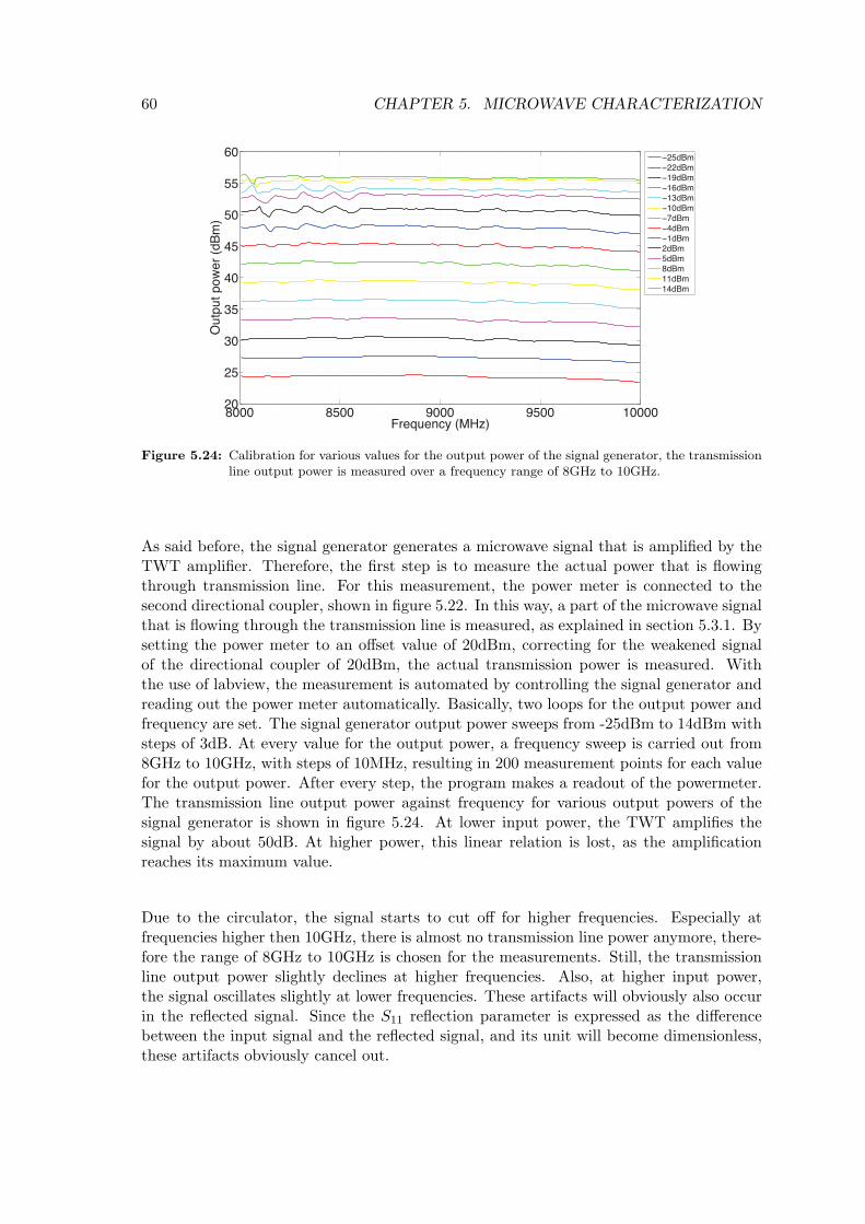
60 CHAPTER 5. MICROWAVE CHARACTERIZATION
8000 8500 9000 9500 1000020
25
30
35
40
45
50
55
60
Frequency (MHz)
Ou
tpu
t p
ow
er
(dB
m)
−25dBm−22dBm−19dBm−16dBm−13dBm−10dBm−7dBm−4dBm−1dBm2dBm5dBm8dBm11dBm14dBm
Figure 5.24: Calibration for various values for the output power of the signal generator, the transmissionline output power is measured over a frequency range of 8GHz to 10GHz.
As said before, the signal generator generates a microwave signal that is amplified by theTWT amplifier. Therefore, the first step is to measure the actual power that is flowingthrough transmission line. For this measurement, the power meter is connected to thesecond directional coupler, shown in figure 5.22. In this way, a part of the microwave signalthat is flowing through the transmission line is measured, as explained in section 5.3.1. Bysetting the power meter to an offset value of 20dBm, correcting for the weakened signalof the directional coupler of 20dBm, the actual transmission power is measured. Withthe use of labview, the measurement is automated by controlling the signal generator andreading out the power meter automatically. Basically, two loops for the output power andfrequency are set. The signal generator output power sweeps from -25dBm to 14dBm withsteps of 3dB. At every value for the output power, a frequency sweep is carried out from8GHz to 10GHz, with steps of 10MHz, resulting in 200 measurement points for each valuefor the output power. After every step, the program makes a readout of the powermeter.The transmission line output power against frequency for various output powers of thesignal generator is shown in figure 5.24. At lower input power, the TWT amplifies thesignal by about 50dB. At higher power, this linear relation is lost, as the amplificationreaches its maximum value.
Due to the circulator, the signal starts to cut off for higher frequencies. Especially atfrequencies higher then 10GHz, there is almost no transmission line power anymore, there-fore the range of 8GHz to 10GHz is chosen for the measurements. Still, the transmissionline output power slightly declines at higher frequencies. Also, at higher input power,the signal oscillates slightly at lower frequencies. These artifacts will obviously also occurin the reflected signal. Since the S11 reflection parameter is expressed as the differencebetween the input signal and the reflected signal, and its unit will become dimensionless,these artifacts obviously cancel out.

5.3. HIGH POWER X-BAND MEASUREMENTS 61
5.3.4 High power samples measurements
The samples were measured ’two-way’. After each measurement, the waveguide was turnedaround and the same measurement was carried out once again. In this way, reflectionparameters S11 and S22 of each sample are determined. For the reflective measurements,the same labview program is used that is used to measure the transmission line output.Only obviously, to measure the reflectivity, the power meter is now connected to the firstdirectional coupler, shown in figure 5.22. By running the labview program a dataset isnow obtained with which the power dependence of the samples reflective character over afrequency range of 8GHz to 10GHz is characterized.
8000
9000
10000
20
40
60−15
−10
−5
0
Frequency (MHz)Output power (dBm)
S11 (dB)
1%5%10%15%20%25%30%
(a)
8000
9000
10000
20
40
60−15
−10
−5
0
Frequency (MHz)Output power (dBm)
S22 (dB)
1%5%10%15%20%25%30%
(b)
Figure 5.25: The reflection S11 (a) and S22 (b) parameters of the second set of samples are shown as afunction of frequency and transmission line output power.
In figure 5.25 the S11 and S22 reflection measurements are plotted. Clearly visible are seven’planes’ indicating the measurements per sample. Roughly it is already visible that thereis no significant power or frequency dependent behaviour, as all planes show no significantgradient.
Therefore, for clarification, the 3D plots are simplified. First, the average S11 and S22
reflectivity over each frequency sweep is plotted against the average transmission lineoutput power over that frequency sweep. These plots are shown in figure 5.26.
20 25 30 35 40 45 50 55 60−14
−12
−10
−8
−6
−4
−2
0
Outputpower (dBm)
S11 (dB)
1%5%10%15%20%25%30%
20 25 30 35 40 45 50 55 60−14
−12
−10
−8
−6
−4
−2
0
Outputpower (dBm)
S22 (dB)
1%5%10%15%20%25%30%
Figure 5.26: The average value of the reflectivity for each frequency sweep is plotted against the averageoutput power of that same frequency sweep. Clearly, there is no significant power dependencein the reflective behaviour of the samples.

62 CHAPTER 5. MICROWAVE CHARACTERIZATION
This way of plotting will cancel out reflective behaviour that is frequency dependent,but it will show reflective behaviour that is dependent on the transmission line outputpower.
This graphs clearly shows a lack of power dependence of the reflective behaviour of thesamples. On average, reflectivity S11 has the same value for varying output power. Onlythe sample with a volume ratio of 15% silver shows a small increase at the highest output-power, but this is probably an artifact.
Besides the average reflectivity against average output power, also the average reflectivityover each output power sweep is plotted against frequency, shown in figure 5.27.
8000 8500 9000 9500 10000−14
−12
−10
−8
−6
−4
−2
0
Frequency (MHz)
S11 (dB)
1%5%10%15%20%25%30%
8000 8500 9000 9500 10000−16
−14
−12
−10
−8
−6
−4
−2
0
Frequency (MHz)
S22 (dB)
1%5%10%15%20%25%30%
Figure 5.27: Average reflectivity S11 (left) and S22 (right) over the transmission line power plotted againstfrequency. Sample with filler ratio of 15% shows a strange decline in reflectivity at higherfrequency. This is probably due to an inhomogenous artifact in the sample, not caused bythe intrinsic behaviour of the homogenous composite material.
This figure shows reflective behaviour that has a frequency dependence, independent ofthe transmission line output power. Especially at higher filler ratios, the reflections showoscillations. This oscillation is caused by the experimental setup, by the length of thewaveguide in particular. The frequency spacing of the oscillation is a measure for thelength of the waveguide as following. Interference of microwaves resulting in maxima inthe reflection will occur when 2d = nλ, with d the length of the waveguide and λ thewavelength. Substituting f = c
λ , where f equals the frequency, gives 2d = n cf . Thedifference between two maxima in the oscillation fn+1-fn =fn=1 gives:
fn+1 − fn =(n+ 1)c
2d− nc
2d=
c
2d(5.2)
The measurements indicate difference between oscillation maxima of about 100MHz, re-sulting in a waveguide length d of about 1.5m, which matches the actual setup. Thisrelation obviously also shows that with a longer waveguide setup this oscillation will be-come smaller. The oscillations are more present at higher filler ratio since the reflectedmicrowave radiation has a higher intensity due to the higher reflectivity. This leads tohigher interference effects.
Furthermore the 15% sample shows interesting behaviour. A clear decline in reflectivityat higher frequencies can be seen for both S11 an S22 reflection parameters. It seems thatthis behaviour is caused by a macroscopic artifact of this sample in particular, as it occurs

5.3. HIGH POWER X-BAND MEASUREMENTS 63
independent from the output power. It is not likely that the behaviour is related to aproperty of the composite material, as the behaviour does not occur at the other samples.Furthermore, when removed, this particular sample showed some spots with a change incolour. This could indicate a change in the composite material, caused by for instancelocal heating on the sample which alters the structure of the sample and herewith theresponse of the sample to an applied microwave signal.
Other notable behaviour is shown by the sample with the filler volume ratio of 1%. Itshows a dip in the signal at around 9000Hz. This could also be an artifact of a non perfecthomogenous composite material.
5.3.5 ’Low power samples’ measurements
Beside the new ’high power’ set of x-band waveguide samples, also high power measure-ments were carried out on three samples remaining from the ’low power samples’, shownin table 5.5. As said earlier, only three samples remained from this set, due to first testmeasurements in which the samples were lost. The measurements are shown in figure 5.28.The reflection coefficients S11 and S22 are plotted against frequency and transmission lineoutput power.
8000
9000
10000
20
40
60−8
−6
−4
−2
0
Frequency (MHz)Output power (dBm)
S11 (dB)
10%20%25%
8000
9000
10000
20
40
60−8
−6
−4
−2
0
Frequency (MHz)Output power (dBm)
S22 (dB)
10%20%25%
Figure 5.28: Reflectivity coefficients S11(left) and S22(right) plotted against transmissionline outputpower and frequency. There seems to be a power dependence in the S11 reflection of the10% sample. The S22 parameter does not show this non linear behaviour.
Immediately, strange behaviour can be seen, as one would expect more or less the samebehaviour in both plots. This is not the case, as the 10% filler ratio sample seems tohave a much higher reflection coefficient S22 than S11. Also, there seems to be a powerdependence in the S11 parameter.
This is more clarified in figure 5.29, in which the average S11 and S22 coefficients overthe frequency sweep are plotted against the average transmission line output power perfrequency sweep. The S11 measurements on the 10% sample clearly shows a power depen-dence of the reflectivity independent of the frequency. At about 50dBm the reflectivity ofthe 10% sample rises significantly to about -3dB. The sample becomes as reflective as the20% sample.
The question obviously rises whether this behaviour can be reproduced and is reversibleand makes this behaviour intrinsic to the material. If this is the case, one would expect
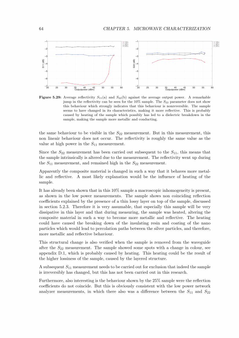
64 CHAPTER 5. MICROWAVE CHARACTERIZATION
20 25 30 35 40 45 50 55 60−7
−6
−5
−4
−3
−2
−1
Outputpower (dBm)
S11 (dB)
10%20%25%
20 25 30 35 40 45 50 55 60−7
−6
−5
−4
−3
−2
−1
Outputpower (dBm)
S22 (dB)
10%20%25%
Figure 5.29: Average reflectivity S11(a) and S22(b) against the average output power. A remarkablejump in the reflectivity can be seen for the 10% sample. The S22 parameter does not showthis behaviour which strongly indicates that this behaviour is nonreversible. The sampleseems to have changed in its characteristics, making it more reflective. This is probablycaused by heating of the sample which possibly has led to a dielectric breakdown in thesample, making the sample more metallic and conducting.
the same behaviour to be visible in the S22 measurement. But in this measurement, thisnon lineair behaviour does not occur. The reflectivity is roughly the same value as thevalue at high power in the S11 measurement.
Since the S22 measurement has been carried out subsequent to the S11, this means thatthe sample intrinsically is altered due to the measurement. The reflectivity went up duringthe S11 measurement, and remained high in the S22 measurement.
Apparently the composite material is changed in such a way that it behaves more metal-lic and reflective. A most likely explanation would be the influence of heating of thesample.
It has already been shown that in this 10% sample a macroscopic inhomogeneity is present,as shown in the low power measurements. The sample shows non coinciding reflectioncoefficients explained by the presence of a thin lossy layer on top of the sample, discussedin section 5.2.3. Therefore it is very assumable, that especially this sample will be verydissipative in this layer and that during measuring, the sample was heated, altering thecomposite material in such a way to become more metallic and reflective. The heatingcould have caused the breaking down of the insulating resin and coating of the nanoparticles which would lead to percolation paths between the silver particles, and therefore,more metallic and reflective behaviour.
This structural change is also verified when the sample is removed from the waveguideafter the S22 measurement. The sample showed some spots with a change in colour, seeappendix D.1, which is probably caused by heating. This heating could be the result ofthe higher lossiness of the sample, caused by the layered structure.
A subsequent S11 measurement needs to be carried out for exclusion that indeed the sampleis irreversibly has changed, but this has not been carried out in this research.
Furthermore, also interesting is the behaviour shown by the 25% sample were the reflectioncoefficients do not coincide. But this is obviously consistent with the low power networkanalyzer measurements, in which there also was a difference between the S11 and S22

5.3. HIGH POWER X-BAND MEASUREMENTS 65
parameter as can be seen in figure 5.12. As already discussed in the previous section, thisis explained by the thin lossy layer present on the sample verified by SEM measurementsshown in appendix E.2.
The rise in reflective behaviour of the 10% sample can also be seen in figure 5.30 whichshows the average reflectivity over the power sweep is plotted against the frequency. TheS22 parameter is clearly much higher than the S11 parameter. Overall, the oscillationcaused by the length of the waveguide setup can be seen in all measurements. The 25%sample here also shows strange behaviour, as the reflectivity overall declines at higherfrequency.
8000 8500 9000 9500 10000−7
−6
−5
−4
−3
−2
−1
Frequency (MHz)
S22 (dB)
10%20%25%
8000 8500 9000 9500 10000−7
−6
−5
−4
−3
−2
−1
Frequency (MHz)
S22 (dB)
10%20%25%
Figure 5.30: Average reflectivity against frequency. Clearly visible is the higher S22 of the 10% sample(left), compared to the S11 value (right).
5.3.6 Reflection coefficients of both sets of samples
It is shown in the previous measurements, that there is no significant power or frequencydependence of the reflective behaviour of the samples, which is reproducible, and thereforeintrinsic to the composite material characteristics. Therefore, it is possible to compare thereflective behaviour of the first set of samples, measured in the low power setup, with theaverage reflection parameters of the second set of samples. Hereby the reproducibility of thedata is checked, and the consistency of behaviour in more or less identical samples.
This comparison is shown in figure 5.31. Here an interesting relation can be seen. Forlower volume ratios, there seems to be a linear dependence between filler ratio and reflec-tive behaviour in dB, or otherwise, a exponential dependence between the filler ratio andreflection expressed as IR
II. Although per volume ratio filler, the samples differ about 1dB
to 2dB, and some samples show non coinciding S11 and S22 reflection coefficients causedby the layered structure, all the samples do match a general trend, in which there seemsto be a saturation point for the 20% sample and up.
At higher volume ratio, reflectivity does not change much anymore. From this roughfit, it can also be concluded that a certain average saturation appears at a filler ratio ofabout in between 15% and 20%. It seems that the saturation value for these samples doesnot limit to 0dB, but a little lower, which means that the composite material never fullyreflects. This is very likely to be caused by the thin nonconducting shell, that surrounds theparticles, which prevents the material from becoming fully metallic and conducting.
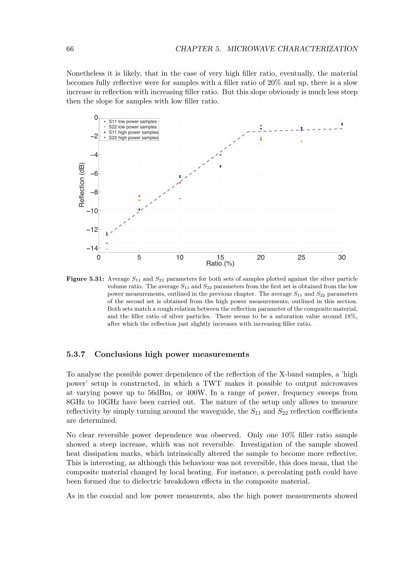
66 CHAPTER 5. MICROWAVE CHARACTERIZATION
Nonetheless it is likely, that in the case of very high filler ratio, eventually, the materialbecomes fully reflective were for samples with a filler ratio of 20% and up, there is a slowincrease in reflection with increasing filler ratio. But this slope obviously is much less steepthen the slope for samples with low filler ratio.
0 5 10 15 20 25 30
−14
−12
−10
−8
−6
−4
−2
0
Ratio (%)
Reflection (dB)
S11 low power samplesS22 low power samplesS11 high power samplesS22 high power samples
Figure 5.31: Average S11 and S22 parameters for both sets of samples plotted against the silver particlevolume ratio. The average S11 and S22 parameters from the first set is obtained from the lowpower measurements, outlined in the previous chapter. The average S11 and S22 parametersof the second set is obtained from the high power measurements, outlined in this section.Both sets match a rough relation between the reflection parameter of the composite material,and the filler ratio of silver particles. There seems to be a saturation value around 18%,after which the reflection just slightly increases with increasing filler ratio.
5.3.7 Conclusions high power measurements
To analyse the possible power dependence of the reflection of the X-band samples, a ’highpower’ setup is constructed, in which a TWT makes it possible to output microwavesat varying power up to 56dBm, or 400W. In a range of power, frequency sweeps from8GHz to 10GHz have been carried out. The nature of the setup only allows to measurereflectivity by simply turning around the waveguide, the S11 and S22 reflection coefficientsare determined.
No clear reversible power dependence was observed. Only one 10% filler ratio sampleshowed a steep increase, which was not reversible. Investigation of the sample showedheat dissipation marks, which intrinsically altered the sample to become more reflective.This is interesting, as although this behaviour was not reversible, this does mean, that thecomposite material changed by local heating. For instance, a percolating path could havebeen formed due to dielectric breakdown effects in the composite material.
As in the coaxial and low power measurents, also the high power measurements showed

5.3. HIGH POWER X-BAND MEASUREMENTS 67
the relation of increasing reflection with increasing filler ratio. When compared to theaverage reflection values from the low power measurements, a rough lineair relation ispresent between the reflection and the filler ratio up to about 17%/18%. Samples with ahigher filler ratio show more or less equal reflection values. This implies an exponentialdependence between the actual reflection expressed as Ir
Iiand filler ratio, since reflection
is expressed in decibel.
Although no quantitative data is obtained about the loss in these measurements, it wasshown that the samples do dissipate energy. A continuous output wave caused the samplesto burn completely. Subsequent measurements were therefore carried out at pulsed wave.Also, remaining samples from the low power measurements which were calculated to havehigh loss, showed coloured burn marks after measuring in the high power setup.
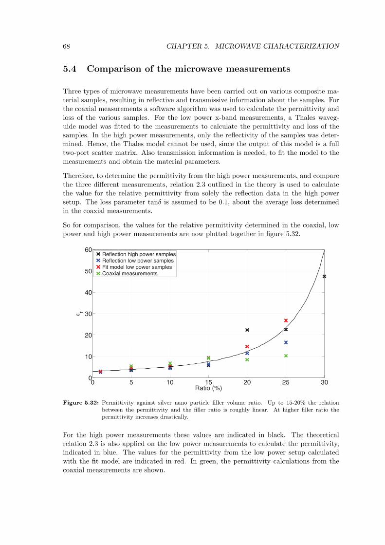
68 CHAPTER 5. MICROWAVE CHARACTERIZATION
5.4 Comparison of the microwave measurements
Three types of microwave measurements have been carried out on various composite ma-terial samples, resulting in reflective and transmissive information about the samples. Forthe coaxial measurements a software algorithm was used to calculate the permittivity andloss of the various samples. For the low power x-band measurements, a Thales waveg-uide model was fitted to the measurements to calculate the permittivity and loss of thesamples. In the high power measurements, only the reflectivity of the samples was deter-mined. Hence, the Thales model cannot be used, since the output of this model is a fulltwo-port scatter matrix. Also transmission information is needed, to fit the model to themeasurements and obtain the material parameters.
Therefore, to determine the permittivity from the high power measurements, and comparethe three different measurements, relation 2.3 outlined in the theory is used to calculatethe value for the relative permittivity from solely the reflection data in the high powersetup. The loss parameter tanδ is assumed to be 0.1, about the average loss determinedin the coaxial measurements.
So for comparison, the values for the relative permittivity determined in the coaxial, lowpower and high power measurements are now plotted together in figure 5.32.
0 5 10 15 20 25 300
10
20
30
40
50
60
Ratio (%)
ε r
Reflection high power samplesReflection low power samplesFit model low power samplesCoaxial measurements
Figure 5.32: Permittivity against silver nano particle filler volume ratio. Up to 15-20% the relationbetween the permittivity and the filler ratio is roughly linear. At higher filler ratio thepermittivity increases drastically.
For the high power measurements these values are indicated in black. The theoreticalrelation 2.3 is also applied on the low power measurements to calculate the permittivity,indicated in blue. The values for the permittivity from the low power setup calculatedwith the fit model are indicated in red. In green, the permittivity calculations from thecoaxial measurements are shown.

5.4. COMPARISON OF THE MICROWAVE MEASUREMENTS 69
0 5 10 15 20 25 30 35 40 4510
0
102
104
106
Ratio (%)
ε r
Reflection high power samplesReflection low power samplesFit model low power samplesCoaxial measurements
Figure 5.33: Same as figure 5.32, but in logarithmic scale.
It is tried to fit the measurements to the various proposed theoretical relations betweenthe permittivity and filler ratio, introduced in the theory in section 2.3. It turned out thatthe measurements are best fitted by relation 2.8, also shown below:
(ε∗)α =(1− Φ)(ε∗m)α
(1− ΦΦc
)(5.3)
For α = 0.3±0.01 and ΦC=0.42±0.01 this relation fits the measurements best. ε∗m, whichrepresents the complex permittivity of the embedding medium is expressed as ε∗m = ε′m −jε′′m or ε∗m = ε′m − jtanδε′m, with ε′m=3 and tanδ=0.003.
Figure 5.33 shows the measurement in log scale. At ΦC of 42% the fit obviously becomesan asymptote.
Mainly two types of interesting behaviour are observed:
• The fit shows a percolation filler ratio of 42%, much higher then a theoretical expectedvalue of about 15-20%
• Up to 15% filler ratio values for the permittivity per sample are roughly in the sameorder. For values with higher filler ratio, values start to differ.
First, this is very likely to be explained by the coating of the particles. The mathematicalexpression assumes a percolation threshold, the point were particles make actual contact.This simply does not occur in the first place, since neighbouring particles will never per-colate. Therefore, the actual percolation threshold from the fit is very doubtful, thoughthe expression for low filler ratio is assumed to be very accurate.
Second, for high filler ratio, it can be seen that values per sample start to differ. Specifically,
70 CHAPTER 5. MICROWAVE CHARACTERIZATION
for the 20% and 25% samples the coaxial measurements and the reflection measurementslead to lower values compared to the other measurements. For the coaxial measurements,this could be explained by the great influence of a non perfect fit, leading to leakage andless reflection, discussed in section 5.1.4. Although the calculations are corrected for thismisfit, especially for high reflective samples, error margins are likely to be much largerthan discussed. A slight misfit for a high dielectric sample could lead to much moreleakage and lower reflection than can be corrected for in the calculation. Concerning thereflection measurements, the assumption of tanδ to be 0.1 is discussable, since the coaxialmeasurements showed higher losses. This would lead to higher permittivity values.
Overall it can be concluded that for low filler ratio values, measurements are more reliable.For higher filler ratio, imperfections seem to influence measurements greatly, leading to awider spread in values.
This can be correlated to the theoretical relation between the permittivity and the reflec-tion, shown in figure 2.4. It can be seen that for a reflection up to -2dB a rough linearrelation between the permittivity and reflection is present. Qualitatively, since these mate-rials have a low reflection coefficient, this makes them dielectric materials by definition. Formaterials that have a reflectivity higher than -2dB, permittivity increases drastically. Itactually becomes an asymptote dependent on the frequency, as the model cannot calculatethe permittivity for reflection up to a certain value.
This high reflection is caused by the material becoming more metallic and less dielectric.The model has trouble describing the material as a dielectric and assigning a value for thepermittivity.
When comparing figure 5.31 and 2.4 it is shown that samples with a reflection coefficienthigher then this -2dB correspond to samples with a filler ratio of ∼20% and higher. Soconsidering the theoretical relation, permittivity increases drastically for samples with ahigher filler ratio and therefore higher reflectivity.
This significant change in permittivity for a change in reflectivity at high filler ratio samplesalso explains the wider spread between the measurements. Imperfections have a greaterinfluence on the reflectivity. For highly reflective samples, this results more significantchanges in the values for the permittivity.
It can be concluded, that the composite material experiences a transition from more di-electric to more metallic behaviour in between 15% and 20% filler particles. Below thispercentage, the material can very well be described as a dielectric material with a di-electric value. Various measurements and samples led to consistent permittivity values.Above this percentage, the material becomes highly reflective and has lost its dielectricproperties.

5.5. CONCLUSIONS RF MICROWAVE MEASUREMENTS 71
5.5 Conclusions RF microwave measurements
This chapter outlines the sample preparation and the RF microwave measurements thathave been carried out on various composite samples. The following research questions werestated for investigation:
• What are the dielectric properties of this composite material, in relation to the ratiofiller particles and epoxy resin?
• What are the loss properties of these composite materials?
• What is the reflective behaviour of the composite materials as a function of the powerof the microwave radiation?
Three different setups have been used:
• A coaxial network analyser setup,
• An X-band network analyser setup
• An X-band high power setup
For these different setups, samples with varying volume ratio silver nanoparticles wereconstructed, to measure the microwave response at varying filler ratio.
In the network analyzer setups, frequency dependent reflection and transmission responsewas obtained, which showed a clear filler ratio dependence, in both coaxial and X-bandmeasurements. Also in the high power X-band measurements, in which only the reflectioncoefficients were determined, this filler ratio dependence was present.
For the X-band samples, the scatter matrix measurements showed strange behaviour, asfor some samples, their reflection coefficients did not coincide. It is shown that the non-coiciding reflection coefficients can only be caused by a gradient in loss. This indicates aninhomogeneity in the samples caused by the construction method. This gradient resultingin non coinciding reflection coeffiecients is most influential on the sample with the highestloss in general.
To determine the material parameters from these scatter matrix coefficients, in the coax-ial measurements, permittivity and loss were determined with a software algorithm. Itis shown that in these calculations the fit of the sample in the sample holder is of greatinfluence, resulting in high error margins in the calculated permittivity. To calculate thematerial parameters from the X-band network analyser measurements, a Thales waveg-uide model was fitted to the scatter matrix measurements. The permittivity from thesereflection measurements was determined by applying the theoretical relation between thereflection of a perpendicular wave in a two interface system and the permittivity.
The permittivity calculations from each measurement were compared and fitted with atheoretical proposed model. This model showed a perfect fit, when a percolation thresholdof 42% volume ratio filler was chosen. This is much higher then values the percolationthreshold described in literature of in between 10-20%. This is explained by the coating ofthe particles, were actual percolation will never occur in the first place in this composite.Therefore, the actual value for the percolation threshold in this fit is very doubtful, though
72 CHAPTER 5. MICROWAVE CHARACTERIZATION
this expression to describe the relation between the permittivity and the filler ratio for lowvalues of the filler ratio is assumed to be very accurate.
So for samples up to 20% there is a well defined relation between filler ratio and permittiv-ity from εr ∼2 to εr ∼8 for 0% to 15%. Permittivity calculations for samples with higherfiller ratio become less accurate, as different measurements lead to different values. Thisimplies a difficulty in describing the material as a dielectric. This uncorrelated behaviouris verified by the theoretical relation between reflection and permittivity. In this relation,for a reflection above ∼-2dB, permittivity increases drastically. Therefore, macroscopicinhomogeneities such as less perfect fit have a more significant influence on the permitiv-ity calculations, as a slight change in reflection and transmission will lead to significantdifferent values for the material parameters. According to the reflection measurements,this -2dB reflection and higher corresponds with a filler ratio in between 15% and 20%and higher. This seems to be the breakpoint between a composite material that can bedescribed as a dielectric, and a more metallic, highly reflective material.
Although the loss calculations from the coaxial and X-band setup are more or less contra-dictive, calculations do indicate a relation, where the lossiness increases for samples with afiller ratio up to this ’transition volume ratio’ of 15-20% with an average loss tanδ of about0.1. It is likely, that samples above this breakpoint have even higher losses, but becauseof their high reflective character, microwaves simply hardly penetrate the material, poweris conserved, which in models will lead to low loss values.
Considering the research goals of possible power dependent reflective behaviour, this be-haviour has not been observed. Though, one of the samples showed a non reversible drasticincrease in reflectivity during a high power measurement. This indicates an intrinsic changein the composite material. Although it turned out not to be reversible, this still indicatesthat microwaves interact with the composite material. Very likely, due to dissipation, abreakdown has occurred, making the composite material more reflective. This behaviouris very interesting for further investigation.

Chapter 6
Conclusions and discussion
This research describes the electrical and microwave characterization of coated silvernanoparticles composite material. Main focus has been the investigation of the presenceof non linear resistive and reflective behaviour. This behaviour is most likely to occur incomposites with a filler ratio near the percolation threshold. This in mind, it is chosen tofabricate and characterize composite material in which silver nanoparticles are used, whichare coated with a thin insulating shell. The following research goals were formulated:
• The fabrication of a composite material of coated silver nanoparticles in a insulatingepoxy resin. Analyzing particles for their composition and presence of a coating inthe first place, then creating homogeneous composite material with a defined varyingfiller ratio.
• Electrical characterization of this composite material. This includes resistance mea-surements and field dependence measurements, to investigate possible non linear fielddependent resistive behaviour.
• The microwave characterization of this composite material at varying conductivefiller ratio. This includes measuring the power dependent reflective and transmissivebehaviour of these composite materials, to investigate a possible power dependencein the reflective behaviour of the composite material. From these measurements thecalculation of the material parameters, relative permittivity εr, relative permeabilityµr and loss tangent tanδ.
Composite material
TEM, SEM and XPS measurements have been carried out for the characterization ofthe silver nanoparticles and composite of nanoparticles in epoxy resin. Were the use ofmicroparticles shows difficulty to create a homogeneous spread through epoxy resin, thisresearch focusses on commercially available silver nanoparticles and epoxy resin, whichresulted in a macroscopic homogeneous spread of particles through the samples. Thepresence of a thin 1-3nm thick coating is verified and ensures no percolation occurs, eventhough at microscopic level, particles do tend to cluster.
73
74 CHAPTER 6. CONCLUSIONS AND DISCUSSION
Electrical characterization
Electrical characterization on composite material with a filler ratio of 25%, above thetheoretical percolation threshold in the macroscopic and microscopic measurements showedthat the material is fully insulating at low voltage. A unique measurement setup forelectrical characterization is constructed. Composite material is deposited on a substratewith microscopically small contacts. In this way, a more defined system is characterizedwere potential is applied over a distinct amount of silver particles. In this setup, two-pointmeasurements have been carried out.
These measurements show a reversible non linear behaviour in the resistance of the com-posite material. In a voltage sweep, with increasing voltage, resistance dropped almostthree orders of magnitude. This effect, considering literature, is very likely the result oftunnel effects between particles close together. It is therefore shown, that a rather simplyfabrication method, were simply nanoparticles are stirred in liquid epoxy, show great po-tential in power dependent non linear resistive behaviour. This is mainly caused by thefact that particles are coated, and although the filler ratio is higher then the theoreticalpercolation threshold, particles will not percolate.
Microwave characterization
For the microwave characterization of the composite material, samples with varying fillerratio have been created. Three different setups were used. In a low power coaxial andX-band waveguide setup, reflection and transmission of the various samples is determined.In a high power setup, the reflection as function of the microwave power is measured.Overall, with increasing filler ratio, reflection increases were transmission decreases.
Some samples showed non coinciding reflection parameters with a spacing up to 2db. Ithas shown that this is caused by a layer structured of the sample with varying loss, as isverified in SEM images. The existence of this multilayered structure is an artifact in thefabrication, but is interesting, since it makes sample very asymmetric in reflection.
To calculate the material parameters, for the coaxial measurements, a software algorithmis used. The low power X-band measurements are fitted to a Thales waveguide model.To determine the material parameters from the high power reflection measurements, thetheoretical expression describing a two interface system is used.
For samples up to 20% there is a well defined relation between filler ratio and permittivityfrom εr ∼2 to εr ∼8. The calculated values perfectly match the proposed model. For higherfiller ratio permittivity calculations become less accurate, as different measurements leadto different values. This implies a difficulty in describing the material as a dielectric.This seems to be the breakpoint between a composite material that can be described as adielectric, and a more metallic, highly reflective material.
Considering the research goal of possible power dependent reflective behaviour, this be-haviour has not been observed. Though, one of the samples showed a non reversible drasticincrease in reflectivity during a high power measurement. This indicates an intrinsic changein the composite material. Although it turned out not to be reversible, this still indicates

75
that microwaves interact with the composite material. Very likely, due to dissipation, abreakdown has occured, making the composite material more reflective. This behaviour isvery interesting for further investigation.
Recommendation
Macroscopic imperfections influence the various measurements. The samples did not showperfect dimensions and air bubbles were occasionally present due to the method of fab-rication. These imperfections are likely the cause of irregularities in the measurements.More practical research should be carried out on the method of fabrication to prevent thesemacroscopic imperfections.
This research has shown the potential of composite material with coated silver nanoparti-cles to show non linear resisitive behaviour. But measurements that showed this behaviouronly qualitatively. The system is not very defined. Tunneling is propably the most im-portant conduction mechanism, but this can only be verified when the actual path with acertain amount of filler particles, over which the voltage is applied, is quantified. In sucha system, the conductive response could be controlled better and tunable. For instance,the spacing between the particles obviously influence the response in resistivity on appliedfield. Resistivity will drop at lower voltage, when particles are closer together. Still, theused setup with composite on microcontacts has shown to be very useful to analyse thisnon linear behaviour. Research on depositing composite material on the contact moreaccurately would be of interest.
Although reversible power dependence in reflective behaviour in the composite with varyingfiller ratio is not observed, an irreversible increase in reflectivity for increasing powerhas been observed. This is likely due to heat dissipation, obviously correlated to thelossy character of the material. It could be interesting to investigate the response of amultilayered structure of layers of composite material with different filler ratio, resultingin different material parameters. This results in asymmetric reflective response, as hasbeen showed, but could have potential in showing power dependent behaviour. A layeredstructure with for instance a thin, highly lossy layer could cause a breakdown in the wholestructure due to heat dissipation, at a certain microwave power.

76 CHAPTER 6. CONCLUSIONS AND DISCUSSION

Bibliography
[1] David M. Pozar. Microwave Engineering. John Wiley and Sons, inc., 1998.
[2] M.I. Skolnik. Radar Handbook. McGraw-Hill, 1970.
[3] D McLachlan and M Heaney. Complex ac conductivity of a carbon black compositeas a function of frequency, composition, and temperature. Physical Review B, Jan1999.
[4] R. Zallen. The Physics of Amorphous Solids. J. Wiley and sons, 1983.
[5] M Connor, S Roy, T Ezquerra, and F Balta Calleja. Broadband ac conductivity ofconductor-polymer composites. Physical Review B, Jan 1998.
[6] G Ruschau, S Yoshikawa, and R Newnham. Resistivities of conductive composites.Journal of Applied Physics, Jan 1992.
[7] H Lee, K Chou, and Z Shih. Effect of nano-sized silver particles on the resistivityof polymeric conductive adhesives. International Journal of Adhesion and Adhesives,page 5, Feb 2005.
[8] Y Rao and C Wong. A novel ultra high dielectric constant epoxy silver compositeforembedded capacitor application. Advanced Packaging Materials, Jan 2002.
[9] C Pecharromn and J Moya. Experimental evidence of a giant capacitance in insulator-conductor composites at the percolation threshold. Adv. Mater, Jan 2000.
[10] D. Stauffer. The Physics of Amorphous Solids. Taylor and Francis, 1987.
[11] S Nakamura, T Minami, G Sawa, and K Kitagawa. Frequency dependence of electricalconduction of composites below the percolation threshold. Electrical Insulation andDielectric Phenomena, Jan 1997.
[12] Y Shen, Y Lin, M Li, and C Nan. High dielectric performance of polymer compositefilms induced by a percolating interparticle barrier layer. Adv. Mater, Jan 2007.
[13] M Koledintseva, P Rawa, R DuBroff, and J Drewniak. Engineering of compositemedia for shields at microwave frequencies. Electromagnetic Compatibility, Jan 2005.
[14] M Achour, M Malhi, J Miane, and F Carmona. Microwave properties of carbon black-epoxy resin composites and their simulation by means of mixture laws. Journal ofApplied Polymer Science, Jan 1999.
77

78 BIBLIOGRAPHY
[15] F Shin, W Tsui, and Y Yeung. Dielectric constant of binary mixtures. Journal ofMaterials Science Letters, Jan 1989.
[16] Shelby Samuel M. Weast, Robert C. Handbook of Chemistry and Physics, 48thedition. Ohio: The chemical Rubber Co, 1967-1968.
[17] L Reimer and H Kohl. Transmission electron microscopy: physics of image formation.books.google.com, Jan 2008.
[18] Vincent B. Crist. Handbooks of Monochromatic XPS spectra. J. Wiley and Sons,2000.
[19] John H. Luft. Improvements in epoxy resin embedding methods. J. Biophys. Biochem.Cytol, 9:409, 1961.
[20] Visser array and phased array antenna basics. page 378, Oct 2006.
[21] Hugh D Young. University physics. 1992.
[22] S.J. Orfanidis. Electromagnetic waves and antennas.

Appendix A
Calculations coaxialmeasurements
0 2 4 6 8 10 12 14 16 185
10
15
20
25
Frequency (GHz)
ε r(ω)
3 3.05 3.1 3.15 3.2 3.256
8
10
12
14
16
Inner diameter sample (mm)
ε r
Figure A.1: εr(ω) at increasing inner diameter of sample(left). Average εr against inner diameter ofsample (right).
0 2 4 6 8 10 12 14 16 185.5
6
6.5
7
7.5
8
8.5
9
9.5
10
Frequency (GHz)
ε r(ω)
6.5 6.55 6.6 6.65 6.7 6.75 6.8 6.85 6.9 6.95 76
7
8
9
10
11
12
13
14
Outer diameter sample (mm)
ε r
Figure A.2: εr(ω) at decreasing outer diameter of sample(left). Average εr against outer diameter ofsample (right).
0 2 4 6 8 10 12 14 16 185
5.5
6
6.5
7
7.5
8
Frequency (GHz)
ε r(ω)
2.7 2.8 2.9 3 3.1 3.2 3.3 3.4
6
6.2
6.4
6.6
6.8
7
7.2
7.4
Thickness sample (mm)
ε r
Figure A.3: εr(ω) at decreasing thichness of sample(left). Average εr against thickness of sample (right).
79

80 APPENDIX A. CALCULATIONS COAXIAL MEASUREMENTS
Appendix B
Low power measurements
A-B, B-A
up, down
Figure B.1: Four symmetry directions of a X-band waveguide.
8 9 10 11 12−20
−15
−10
−5
0
Frequency (GHz)
dB
S11
S12
S21
S22
S11/22
fit
S12/21
fit
8 9 10 11 12−20
−15
−10
−5
0
Frequency (GHz)
dB
S11
S12
S21
S22
S11/22
fit
S12/21
fit
8 9 10 11 12−20
−15
−10
−5
0
Frequency (GHz)
dB
S11
S12
S21
S22
S11/22
fit
S12/21
fit
8 9 10 11 12−20
−15
−10
−5
0
Frequency (GHz)
dB
S11
S12
S21
S22
S11/22
fit
S12/21
fit
Up, A - B Down, A - B
Up, B - A Down, B - A
Figure B.2: f = 5% sample.
81
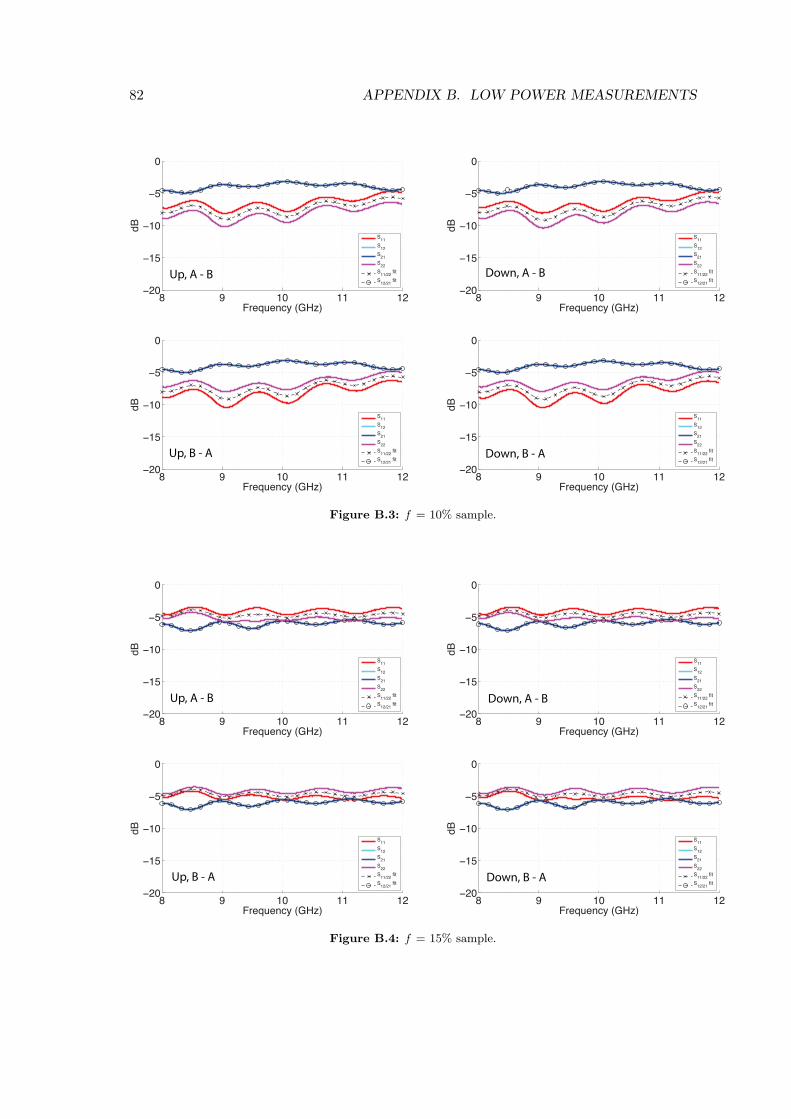
82 APPENDIX B. LOW POWER MEASUREMENTS
8 9 10 11 12−20
−15
−10
−5
0
Frequency (GHz)
dB
S11
S12
S21
S22
S11/22
fit
S12/21
fit
8 9 10 11 12−20
−15
−10
−5
0
Frequency (GHz)
dB
S11
S12
S21
S22
S11/22
fit
S12/21
fit
8 9 10 11 12−20
−15
−10
−5
0
Frequency (GHz)
dB
S11
S12
S21
S22
S11/22
fit
S12/21
fit
8 9 10 11 12−20
−15
−10
−5
0
Frequency (GHz)
dB
S11
S12
S21
S22
S11/22
fit
S12/21
fit
Up, A - B Down, A - B
Up, B - A Down, B - A
Figure B.3: f = 10% sample.
8 9 10 11 12−20
−15
−10
−5
0
Frequency (GHz)
dB
S11
S12
S21
S22
S11/22
fit
S12/21
fit
8 9 10 11 12−20
−15
−10
−5
0
Frequency (GHz)
dB
S11
S12
S21
S22
S11/22
fit
S12/21
fit
8 9 10 11 12−20
−15
−10
−5
0
Frequency (GHz)
dB
S11
S12
S21
S22
S11/22
fit
S12/21
fit
8 9 10 11 12−20
−15
−10
−5
0
Frequency (GHz)
dB
S11
S12
S21
S22
S11/22
fit
S12/21
fit
Up, A - B Down, A - B
Up, B - A Down, B - A
Figure B.4: f = 15% sample.

83
8 9 10 11 12−20
−15
−10
−5
0
Frequency (GHz)
dB
S11
S12
S21
S22
S11/22
fit
S12/21
fit
8 9 10 11 12−20
−15
−10
−5
0
Frequency (GHz)
dB
S11
S12
S21
S22
S11/22
fit
S12/21
fit
8 9 10 11 12−20
−15
−10
−5
0
Frequency (GHz)
dB
S11
S12
S21
S22
S11/22
fit
S12/21
fit
8 9 10 11 12−20
−15
−10
−5
0
Frequency (GHz)
dB
S11
S12
S21
S22
S11/22
fit
S12/21
fit
Up, A - B Down, A - B
Up, B - A Down, B - A
Figure B.5: f = 20% sample.
8 9 10 11 12−20
−15
−10
−5
0
Frequency (GHz)
dB
S11
S12
S21
S22
S11/22
fit
S12/21
fit
8 9 10 11 12−20
−15
−10
−5
0
Frequency (GHz)
dB
S11
S12
S21
S22
S11/22
fit
S12/21
fit
8 9 10 11 12−20
−15
−10
−5
0
Frequency (GHz)
dB
S11
S12
S21
S22
S11/22
fit
S12/21
fit
8 9 10 11 12−20
−15
−10
−5
0
Frequency (GHz)
dB
S11
S12
S21
S22
S11/22
fit
S12/21
fit
Up, A - B Down, A - B
Up, B - A Down, B - A
Figure B.6: f = 25% sample.

84 APPENDIX B. LOW POWER MEASUREMENTS

Appendix C
Microwave properties
Table C.1: Specific frequency bands in the microwave spectrum
L band 1 to 2 GHzS band 2 to 4 GHzC band 4 to 8 GHZX band 8 to 12 GHzKu band 12 to 18 GHzK band 18 to 26.5 GHzKa band 26.5 to 40 GHzQ band 30 to 50GHzU band 40 to 60 GHzV band 50 to 75GHzE band 60 to 90GHzW band 75 to 110 GHzF band 90 to 140 GHzD band 110 to 170 GHZ
Table C.2: The loss tangent of some material commonly used in the microwave industry, at two differentfrequencies.
tanδMaterial 100MHz 10GHzAir 0 0PTFE (Teflon) 0.0002 0.00015Polyethylene 0.0002 0.00031Polystyrene 0.0001 0.0007FR-4 0.021 0.021Rogers Ro4003C 0.0027coax samples ∼0.05 ∼0.05 <εr<∼ 0.2
85

86 APPENDIX C. MICROWAVE PROPERTIES

Appendix D
Discoloration X-band sample
Figure D.1: A coloured spot on the 10% sample likely to be caused by heating is visible in the middel ofthe sample.
87

88 APPENDIX D. DISCOLORATION X-BAND SAMPLE
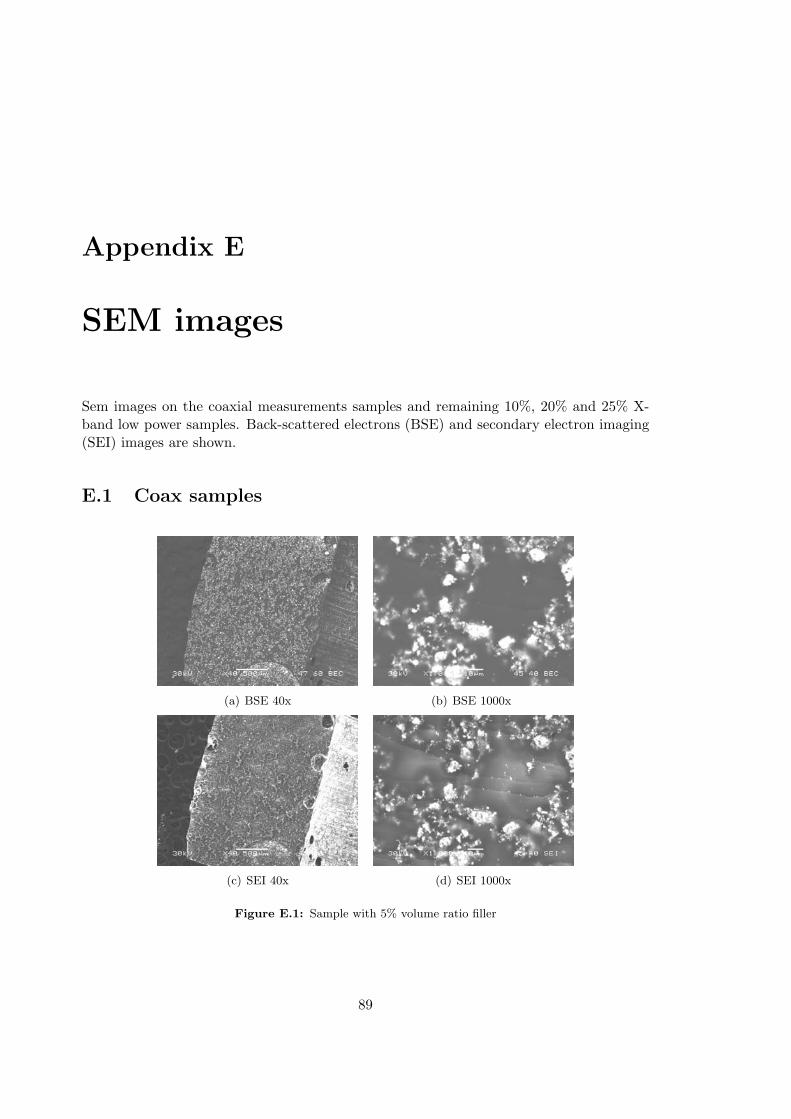
Appendix E
SEM images
Sem images on the coaxial measurements samples and remaining 10%, 20% and 25% X-band low power samples. Back-scattered electrons (BSE) and secondary electron imaging(SEI) images are shown.
E.1 Coax samples
(a) BSE 40x (b) BSE 1000x
(c) SEI 40x (d) SEI 1000x
Figure E.1: Sample with 5% volume ratio filler
89
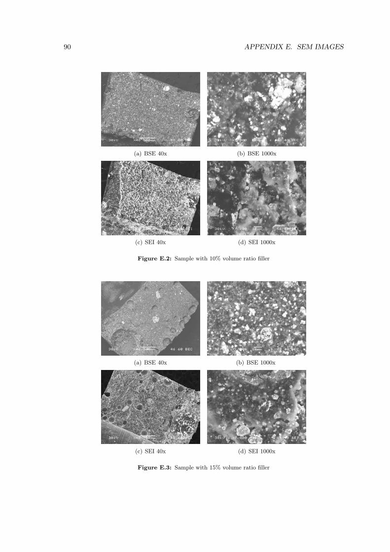
90 APPENDIX E. SEM IMAGES
(a) BSE 40x (b) BSE 1000x
(c) SEI 40x (d) SEI 1000x
Figure E.2: Sample with 10% volume ratio filler
(a) BSE 40x (b) BSE 1000x
(c) SEI 40x (d) SEI 1000x
Figure E.3: Sample with 15% volume ratio filler

E.1. COAX SAMPLES 91
(a) BSE 40x (b) BSE 1000x
(c) SEI 40x (d) SEI 1000x
Figure E.4: Sample with 20% volume ratio filler
(a) BSE 40x (b) BSE 1000x
(c) SEI 40x (d) SEI 1000x
Figure E.5: Sample with 25% volume ratio filler
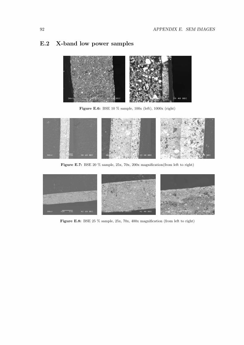
92 APPENDIX E. SEM IMAGES
E.2 X-band low power samples
Figure E.6: BSE 10 % sample, 100x (left), 1000x (right)
Figure E.7: BSE 20 % sample, 25x, 70x, 200x magnification(from left to right)
Figure E.8: BSE 25 % sample, 25x, 70x, 400x magnification (from left to right)