ee 201803 cover dum kc - evaluationengineering.com · 2 evaluationengineering.com march 2018...
TRANSCRIPT

EE_201803_COVER_DUM_KC.indd 2EE_201803_COVER_DUM_KC.indd 2 2/12/2018 9:43:59 AM2/12/2018 9:43:59 AM

Switching | Simulation | Programmable Resistors | Custom Design | Connectivity & Cables
Designed for Today’s Most Demanding Electronic Test & Verification Applications
Pickering PXI Switching & Simulation
We Already Have Your Solution
Visit www.rsleads.com/803ee-007
EE201803_AD Pickering.indd COVERIIEE201803_AD Pickering.indd COVERII 2/8/2018 8:57:48 AM2/8/2018 8:57:48 AM

evaluationengineering.comMarch 2018 1
March 2018, Vol. 57, No. 3
EE-EVALUATION ENGINEERING (ISSN 0149-0370). Published monthly by NP Communications, 2477 Stickney Point Rd., Ste. 221-B, Sarasota, FL 34231. Subscription rates: $176 per year in the United States; $193.60 per year in Canada/Mexico; International subscriptions are $224.40 per year. Current single copies, (if available) are $15.40 each (U.S.); $19.80 (international). Back issues, if available, are $17.60 each (U.S.) and $22 (international). Payment must be made in U.S. funds on a branch of a U.S. bank within the continental United States and accompany request. Subscription inquiries: [email protected].
Title® registered U.S. Patent Offi ce. Copyright© 2018 by NP Communications LLC. All rights reserved. No part of this publication may be reproduced or transmitted in any form or by any means, electronic or mechanical, including photocopy, recording, or any information storage-and-retrieval system, without permission in writing from the publisher.
Offi ce of publication: Periodicals Postage Paid at Sarasota, FL 34276 and at additional mailing offi ces. Postmaster: Send address changes to EE-EVALUATION ENGINEERING, P.O. BOX 17517, SARASOTA FL 34276-0517
Written by Engineers…for Engineers evaluationengineering.com
@EE_Engineers
www.facebook.com/EvaluationEngineering
C O N T E N T S
I N S T R U M E N TAT I O N
SPECIAL REPORT
Power supplies/loads6 Controlling power for today’s
applicationsby Rick Nelson, Executive Editor
SPECIAL REPORT
Optical Communications10 Taking a fresh look at optical
technologiesby Rick Nelson, Executive Editor
Industry Happenings26 DesignCon highlights IP and
interconnect as well as test and measurementby Rick Nelson, Executive Editor
S E M I C O N D U C TO R T E S T
Cybersecurity18 Simulation for strategic hardware
Trojans testingby Kevin Kwiat, Haloed Sun TEK LLC,
and Frank Born, Just Born Tech LLC
C O M P O N E N T S
Industry Happenings22 IEDM sees transistor, memory, laser
innovationsby Rick Nelson, Executive Editor
Product Focus28 Power transistors, drivers, controllers
energize diverse array of productsby Rick Nelson, Executive Editor
C O M P O N E N T S
Technology Insights32 Nanoimprinting scales up imaging,
sensing, spectroscopy applicationsby Rick Nelson, Executive Editor
D E PA R T M E N T S
2 Editorial
4 EE Industry Update
30 EE Product Picks
31 Index of Advertisers
01_EE_201803_TOC_MECH_KC.indd 101_EE_201803_TOC_MECH_KC.indd 1 2/12/2018 11:23:19 AM2/12/2018 11:23:19 AM
March 2018evaluationengineering.com2
EDITORIAL
NP COMMUNICATIONS LLC2477 Stickney Point Rd., Suite 221BSarasota, Florida 34231Phone: 941-388-7050•Fax: 941-388-7490
Publishers of this magazine assume no responsibility for statements made by their advertisers in business competition, nor do they assume responsibility for statements/opinions, expressed or implied, in the columns of this magazine.
Printed in the U.S.A.
evaluationengineering.com
EDITORIAL
EXECUTIVE EDITOR Rick Nelsone-mail: [email protected]
MANAGING EDITOR Ken Cormiere-mail: [email protected]
PRODUCTION
AD CONTRACTS/TRAFFIC MANAGER Laura Moultone-mail: [email protected]
BUSINESS
PRESIDENT Kristine Russelle-mail: [email protected]
PUBLISHER Jim Russelle-mail: [email protected]
ASSOCIATE PUBLISHER Michael Hughese-mail: [email protected]
MARKETING DIRECTOR Joan Sutherland
ADVERTISINGWEST
Michael Hughes Phone: 805-529-6790e-mail: [email protected]
EASTBlake Holton or Michelle Holton
Phone: 407-971-6286 or 407-971-8558e-mail: bholton@cfl .rr.com
mmholton@cfl .rr.com
CIRCULATIONSUBSCRIPTIONS / BACK ISSUES
e-mail: [email protected]
LIST RENTALS Laura Moulton e-mail: [email protected]
EPRODUCT COORDINATOR Mary Haberstroh e-mail: [email protected]
REPRINTS Evelyn Dodgee-mail: [email protected]
EE-EVALUATION ENGINEERING is available by free subscription to qualifi ed managers, supervisors
and engineers in the electronics and related industries.
FOUNDER A. VERNER NELSONe-mail: [email protected]
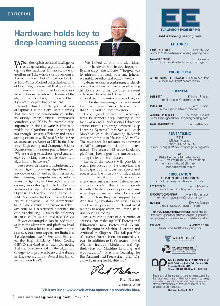
RICK NELSON
Executive Editor
Visit my blog: www.evaluationengineering.com/ricks-blog/
When the topic is artifi cial intelligence or deep learning, algorithms tend to
capture the headlines. But an accurate al-gorithm isn’t the whole story. Speaking at the International Test Conference last fall in Fort Worth, Michael Schuldenfrei, CTO of Optimal+, commented that great algo-rithms aren’t suffi cient. The key to success, he said, lies in the infrastructure—not the algorithms. “Great algorithms won’t help if you can’t deploy them,” he said.
Infrastructure from the point of view of Optimal+ is the global data highway that connects the semiconductor indus-try-supply chain—fabless companies, foundries, and OSATs, for example. Also important are the hardware platforms on which the algorithms run. “Accuracy is not enough—energy effi ciency and speed are important as well,” said Vivienne Sze, an associate professor at MIT in the Elec-trical Engineering and Computer Science Department, in a recent phone interview. “We are trying to address speed and en-ergy by looking across whole stack from algorithm to hardware.”
Sze’s research interests include energy-aware signal-processing algorithms and low-power circuit and system design for deep learning, computer vision, autono-mous navigation, and image/video pro-cessing. Work during 2015 led to the pub-lication of a paper she coauthored titled “Eyeriss: An Energy-Effi cient Reconfi gu-rable Accelerator for Deep Convolutional Neural Networks.” At the International Solid State Circuits Conference in Febru-ary 2016, MIT researchers described the chip as achieving 10 times the effi ciency of a mobile GPU, as reported in MIT News.
Power consumption can be addressed at both the algorithm and platform level. “You can do a lot from a hardware per-spective, but some aspects are limited to the algorithm itself,” Sze said. She cit-ed the High Effi ciency Video Coding (HEVC) standard as an example, noting that she was involved in the algorithm changes to improve effi ciency. She shared an Engineering Emmy Award last fall for her work on HEVC.
“We looked at both the algorithms and the hardware side in developing theEyeriss chip,” she told me. “The goal was to address the needs of a smartphone, wearable, or other embedded device.”
Extensive work is continuing on devel-oping the fast and effi cient deep-learning hardware platforms. Sze cited a recent article in The New York Times noting that at least 45 companies are working on chips for deep-learning applications—at least fi ve of which have each raised more than $100 million from investors.
The design of effi cient hardware sys-tems to support deep learning is the focus of an MIT Professional Education course titled “Designing Effi cient Deep Learning Systems” that Sze will teach March 28-29 at the Samsung Research America campus in Mountain View, CA. The course will be repeated this summer on MIT’s campus at a date to be deter-mined. The course will cover hardware platforms, how algorithms run on them, and optimization techniques.
Sze said the course will provide a broad perspective of the deep-learning landscape with a focus on speed and power and the interplay of algorithms and hardware. Algorithm developers in attendance can learn how platforms vary and how to adapt their code to run ef-fi ciently. Hardware developers can learn what type of neural networks are out there and how they can support them. And fi nally, investors can gain insights about what questions to ask and what metrics to apply when evaluating start-ups seeking funding.
Sze’s course is part of a portfolio of courses that make up MIT Professional Education’s new Professional Certifi -cate Program in Machine Learning and Artifi cial Intelligence. The full portfolio of courses hasn’t been announced yet, but—in addition to Sze’s course—initial offerings include “Modeling and Op-timization for Machine Learning and Applications,” “Machine Learning for Big Data and Text Processing,” and “Ma-chine Learning for Healthcare.”
Hardware holds key to deep-learning success
02_EE_201803_Editorial_MECH_KC.indd 202_EE_201803_Editorial_MECH_KC.indd 2 2/8/2018 3:49:27 PM2/8/2018 3:49:27 PM

Ensure Your Products PerformTest with the Interpower® International Power Source
Product testing is essential during product development, especially when designing for global markets. Using an AC power source can assist in testing that product at various voltages and frequencies.
By testing during the design phase, the International Power Source can help to ensure the product will perform correctly and may help to prevent potentially expensive modifications after the end product is in production. An AC power source can be used for technical work and allow precision control of the voltage, current, and frequency.
Interpower International Power Source• Provides a clean, convenient source of AC power for product design• Provides product testing at various voltages and frequencies found around the world• Includes seven of most common country-specific sockets• Models available with RS232 and USB ports; models available with no communication ports• Interface software package available (allows user to create programmable routines)
Models are Available for Purchase or RentContact Customer Service for more details. Interpower offers free technical support.
INTERPOWER | P.O. Box 115 | 100 Interpower Ave | Oskaloosa, IA 52577 | Toll-Free Phone: (800) 662-2290 | Toll-Free Fax: (800) 645-5360 | [email protected]
ORDER A FREE CATALOG TODAY! E-mail [email protected] or call toll-free.
Order Online! www.interpower.com
Business Hours: 7 a.m.–6 p.m. Central Time
®
®
TThhee IInntteerrppoowweerr IInntteerrnattiional Power Source is an AC power source that can provide product testing in the lab and can assist companies wanting to export.
Visit www.rsleads.com/803ee-004
EE201803_AD Interpower.indd 3EE201803_AD Interpower.indd 3 2/8/2018 8:58:33 AM2/8/2018 8:58:33 AM

March 2018evaluationengineering.com4
INDUSTRYUPDATE
$12,012.1 millionProjection of total market for sensors
in surveillance and security by 2023
Source: Frost & Sullivan
80 millionAutomobile units churned out by
manufacturers globally in 2017
69%Worldwide percentage of 2023 auto sales
predicted to be connected cars
77%Market share for direct LED backlit TVs
in Q2, Q3, and Q4 in 2017, up from 69% in 2016
Source: IHS Markit
$57 billionPredicted spending on fab equipment
during 2018Source: SEMI
21.5%Increase in semiconductor sales globally
year-to-year for month of November Source: Semiconductor Industry Association
$123 billionProjection for robotics market sector by
2026Source: IDTechEx
30 billionExpected numbers of Internet of Things-
enabled devices globally by 2020.Source: Goldman Sachs
$300 millionForecast for world graphene market by
2027 Source: IDTechEx
Chinese fi rm completes deal to buy U.S. semiconductor companyThe dollar numbers are relatively small—$15 million—in the purchase of Al-lentown, PA, semiconductor-equipment maker Akrion Systems LLC, by Beijing-based Naura Microelectronics Equipment Co. Ltd. The more noteworthy aspect of the transaction might be the approval for it in January by the Committee on Foreign Investment in the United States (CFIUS), which has tightened restrictions on the purchase of U.S. assets by Chinese com-panies. “As far as we are aware, this is the fi rst Chinese acquisition of a U.S. com-pany to be approved by CFIUS under the Trump Administration,” Gibson Dunn & Crutcher LLP partner Fang Xue, one of the deal lawyers representing Naura, was quoted by Reuters as saying.
CFIUS has been wary in the past of semi-conductor-related purchases by Chinese interests, because of worries about poten-tial transfers of sensitive technology. Last year, an attempted $1.3 billion purchase of U.S. chipmaker Lattice Semiconductor Corp. by Canyon Bridge Capital Partners LLC, a U.S.-based company funded by the Chinese government, was blocked by CFIUS and the White House. Akrion, how-ever, provides machinery to other compa-nies that prepares chips for use.
Another similar deal awaits approval by the CFIUS—the acquisition of semi-conductor testing concern Xcerra Corp for $580 million by China-linked Unic Capi-tal Management.
ISS Europe to spotlight workforce developmentSEMI has announced that SEMI Europe’s Industry Strategy Symposium (ISS Eu-rope), coming on the heels of ISS 2018 in the U.S., will highlight STEM educa-tion and a talent pipeline, critical issues to electronics manufacturing executives sharpening their competitive edge in the global supply chain. Day 2 of the fl agship business event—March 4-6 in Dublin, Ire-land—will feature two experts focusing on how companies can “Gain, Train and Re-tain World-Class Talent.”
Ann-Charlotte Johannesson, CEO, CEI-Europe AB, will examine strategies to at-tract, retain, and develop highly skilled workers in the semiconductor industry as an essential component of Europe´s global competitiveness in her presentation “Smart Training for Smarter Engineers—The Way of Ensuring the Competitive Advantage for the Global European In-dustry.” CEI-Europe has developed, orga-nized, and held short technology courses across Europe for more than three decades.
Cheryl Miller, founder/executive direc-tor, Digital Leadership Institute, will pres-
ent an overview of education and digital skills, innovation, entrepreneurship, and the workplace of the future. The Digital Leadership Institute, a Brussels-based in-ternational NGO, is a recognized world leader in promoting greater participation of girls and women in strategic, innovative ESTEAM (Entrepreneurship & Arts pow-ered by STEM).
“A skilled workforce is not only a key-stone to the success of the global supply chain but a source of competitive advan-tage, making STEM education and a strong talent pipeline critical focus areas for the industry,” said Laith Altimime, president, SEMI Europe. “SEMI member companies feel the pinch, with thousands of open positions that are critical to sustaining the pace of innovation and growth. To address the talent shortfall, SEMI Europe this year launched a workforce development and diversity initiative.”
Other ISS Europe 2018 highlights in-clude the panel discussion “Critical Strate-gies to Grow Europe in the Global Supply Chain,” the opening networking recep-tion, a gala dinner, and the 2017 European Award ceremony.
Engineers develop fl exible, water-repellent graphene circuits for washable electronicsNew graphene printing technology can produce electronic circuits that are low-cost, fl exible, highly conductive, and wa-ter repellent. The nanotechnology “would lend enormous value to self-cleaning wearable/washable electronics that are re-sistant to stains, or ice and biofi lm forma-tion,” according to a recent paper describ-ing the discovery.
“We’re taking low-cost, inkjet-printed graphene and tuning it with a laser to make functional materials,” said Jonathan Claussen, an Iowa State University assis-tant professor of mechanical engineering, an associate of the U.S. Department of Energy’s Ames Laboratory and the corre-sponding author of the paper recently fea-tured on the cover of the journal Nanoscale, as quoted at Newswise.
The paper, entitled “Superhydrophobic inkjet printed fl exible graphene circuits via direct-pulsed laser writing,” describes
The Clontarf Castle, Dublin, Ireland, site for ISS Europe, March 4-6.Courtesy of Clontarf Castle
04-05_EE_201803_IndUpdate_MECH_KC.indd 404-05_EE_201803_IndUpdate_MECH_KC.indd 4 2/8/2018 3:47:55 PM2/8/2018 3:47:55 PM

evaluationengineering.comMarch 2018 5
INDUSTRYUPDATE
For more on these and other news items, visit www.evaluationengineering.com/category/industry-update/
how Claussen and the nanoengineers in his research group use inkjet printing tech-nology to create electric circuits on fl exible materials. In this case, the ink is fl akes of graphene—the wonder material can be a great conductor of electricity and heat, plus it’s strong, stable, and biocompatible.
The printed fl akes, however, aren’t highly conductive and have to be pro-cessed to remove nonconductive binders and weld the fl akes together, boosting conductivity and making them useful for electronics or sensors.
That post-print process typically in-volves heat or chemicals. But Claussen and his research group developed a rapid-pulse laser process that treats the graphene without damaging the printing surface—even if it’s paper.
And now they’ve found another appli-cation of their laser processing technology: taking graphene-printed circuits that can hold water droplets (they’re hydrophilic) and turning them into circuits that repel water (they’re superhydrophobic).
“We’re micro-patterning the sur-face of the inkjet-printed graphene,” Claussen said. “The laser aligns the graphene fl akes vertically—like little pyramids stacking up. And that’s what induces the hydrophobicity.”
Claussen said the energy density of the laser processing can be adjusted to tune the degree of hydrophobicity and conductiv-ity of the printed graphene circuits.
And that opens up all kinds of possi-bilities for new electronics and sensors, ac-cording to the paper.
“One of the things we’d be interested in developing is anti-biofouling materials,” said Loreen Stromberg, a paper coauthor and an Iowa State postdoctoral research associate in mechanical engineering and for the Virtual Reality Applications Center. “This could eliminate the buildup of bio-logical materials on the surface that would inhibit the optimal performance of devices such as chemical or biological sensors.”
The technology could also have ap-plications in fl exible electronics, wash-able sensors in textiles, microfl uidic technologies, drag reduction, de-icing,
electrochemical sensors, and technology that uses graphene structures and electri-cal simulation to produce stem cells for nerve regeneration.
The researchers wrote that further stud-ies should be done to better understand how the nano- and microsurfaces of the printed graphene creates the water-repel-ling capabilities.
Peregrine Semiconductor changes name to pSemiPeregrine Semiconductor, a Murata com-pany, has changed its name to pSemi, as it marks its 30-year anniversary. The fi rm says its semiconductor team intends to broaden its scope and expand its prod-uct portfolio. Building on its founda-tion in RF integration, pSemi’s product portfolio will span power management, connected sensors, optical transceivers, antenna tuning, and RF frontends.
“We’ve challenged the pSemi team to broaden their scope, increase their intel-lectual property portfolio, and grow on a global scale to support more semiconduc-tor innovations,” said Norio Nakajima, senior executive vice president, module business unit, at Murata, in a press re-lease. “As a Murata company, pSemi will leverage the breadth of Murata’s manu-facturing and technology leadership, while maintaining a level of autonomy that accelerates its path to semiconduc-tor integration. pSemi will serve as the hub for Murata’s semiconductor activi-ties, and we are investing in its aggres-sive growth strategy to fuel our move into more advanced and intelligent modules.”
IN BRIEF •Frost & Sullivan recently honored Cop-
per Mountain Technologies (CMT) with its 2017 Global Product Leadership award, in recognition for its accomplishments with USB VNAs. CMT has introduced a range of instruments aligned with the growing customer requirements for less expensive, small, more portable, and higher-performance VNAs over the past 10 years.
•Marvin Test Solutions announced that
the company is a member of the BAE Sys-tems-led team that won the U.S. Air Force Bomber Armament (BAT) program com-petition in September 2017. The BAT will be the U.S. Air Force’s common armament tester for the B-1B, B-2A, and B-52H, sup-porting fl ightline and intermediate-level testing of all bomb ejector racks, rotary launchers, and pylon assemblies used the nation’s bomber fl eet. MTS will be a signif-icant provider of hardware, software, and design support for the BAT Core Tester. The contract value of $64 million provides for the design, development, manufactur-ing, and sustainment of the Bomber Arma-ment Tester system.
•Qualcomm Inc., headquartered in San Diego, CA, says it has won antitrust ap-proval by the European Union and South Korea for its $39 billion purchase of NXP Semiconductors NCV. The approvals edge the company closer to becoming one of the top suppliers of chips used in au-tomobiles, as technology becomes ubiqui-tous in the auto industry.
•Texas Instruments announced that its board of directors has selected Brian Crutch-er to become the com-pany’s next president and CEO, effective June 1. Crutcher, a 22-year veteran of TI, succeeds current presi-dent and CEO Rich Templeton, who will transition out of the roles over the next few months, but will remain the company’s chairman.
•According to a Financial Times report, Toshiba is considering an IPO of its memory chip business if a proposed sale to a Bain Capital-led consortium does not garner antitrust approval by March 31. The report said that the IPO is one of vari-ous contingency plans being looked at by Toshiba’s top executives. The fi rm agreed to sell Toshiba Memory last September to cover billions of dollars in liabilities from its now defunct U.S. nuclear power unit, Westinghouse Electric Co. LLC.
Engineers create method for vaporizing electronicsWhen electronics containing sensitive data get into the wrong hands, what can be done to protect that information? According to an article in the Cornell Chronicle, engi-neers from Cornell and Honeywell Aero-space have come up with a new method for electronics to self-destruct, using radio waves as a trigger from a remote location. Their technique uses a silicon dioxide mi-
A polycarbonate shell 125 microns thick after a vaporization test of its embedded rubidium and sodium bifl uorideCourtesy of Cornell University
crochip attached to a polycarbonate shell. Inside the shell are microscopic cavities containing rubidium and sodium bifl uo-ride. Valves on the cavities can be opened via radio waves, creating a thermal reac-tion, vaporizing the polycarbonate shell, and decomposing the sodium bifl uoride. Resultant hydrofl uoric acid etches away the electronics.
Brian CrutcherCourtesy of Texas Instruments
04-05_EE_201803_IndUpdate_MECH_KC.indd 504-05_EE_201803_IndUpdate_MECH_KC.indd 5 2/8/2018 3:48:04 PM2/8/2018 3:48:04 PM

March 2018evaluationengineering.com6
SPECIAL REPORT P OW E R SUPPL I E S/LOADS
In pursuit of clean power and effi ciency in applications rang-ing from consumer to military and aerospace, vendors are making advancements in areas including power supplies and
loads, semiconductor technology, and instruments that can assist in power measurements.
Jon Semancik, director of marketing, AMETEK Programmable Power, highlighted the breadth of industries that power technol-ogy serves. “AMETEK Programmable Power serves a growing range of applications, including commercial and military avionics testing, general R&D, automated testing equipment, electromag-netic compatibility (EMC) compliance testing, semiconductor fab-rication, oil exploration, solar-array and battery-string simulation, AC power simulation, manufacturing and process control, and IEC standards testing,” he said.
As for challenges customers are facing, Semancik explained, “Our customers are always striving to reduce the footprint of any test system or simulation system they confi gure, and the high power density of our Asterion line (Figure 1) is one way that we’re helping them accomplish that.” He continued, “They’ve asked us for instruments that are easier to use and more fl exible, and we think our intuitive touchscreen front panels go a long way toward achieving that goal. They also want instruments that simplify test setup and execution; the auto-paralleling function in the Asterion supplies make system confi guration and synchro-nization simpler.”
Semancik elaborated on the company’s power-supply offer-ings. “Our Asterion high-power AC sources can output up to 3 kVA from a 1U package, and even higher outputs when multiple units are stacked. Our 3-phase, 2U sources offer similar power density advantages.” He said auto-paralleling capability sim-plifi es stacking—allowing users to combine up to six units to achieve up to 18,000 VA of output power. “One unit becomes the master while the rest serve as auxiliary units,” he said. “Multi-chassis confi gurations like these are confi gured automatically when the chassis are interconnected with the interface cables. There’s no user setup required, except to wire the outputs. The chassis are automatically synchronized.”
Commenting on usability, he said, “In addition to the standard Ethernet LXI, USB, and RS-232 control interfaces and optional GPIB control interface, Asterion supplies provide an intuitive touchscreen interface. The touchscreen home page offers access to a menu of dashboards, output programming parameters, mea-surements, sequencing, confi guration, control interfaces, applica-
tions, and system settings tools, all available with the touch of an icon. A dynamic rate-change algorithm adjusts the control resolu-tion to combine precise control over small parameter changes with quick sweeps through the entire range. Output waveforms can be displayed through the touchscreen or the Asterion Virtual Panels Windows-based graphical user interface.”
He also commented on the company’s trademarked iX2 cur-rent-doubling technology.1 “The iX2 technology built into Asterion AC power sources allows overcurrent capability up to twice its nominal max current, resulting in a full 200% overcurrent capabil-ity,” he said, thereby allowing for full-power operation over 75% of the source’s voltage output ranges. “The iX2 current-doubling technology also eliminates the need to buy multiple sources or overpowered sources to run tests at different voltage levels, such as when performing low-line voltage testing,” he added.
For customers in the avionics testing business, he said, Asterion power supplies have a range of avionics electrical power quality test software packages developed for popular military and com-mercial aircraft. These avionics testing packages provide custom-ers with simple-to-use testing solutions for which the intensive test sequence programming is done already.
Supplies plus loadsChroma Systems Solutions offers a variety of equipment for pow-er, safety, and component testing, said Larry Sharp, senior appli-cations engineer. “Chroma’s R&D [team] creates hardware and software to support a variety of test requirements,” he said, citing as examples electric-vehicle, battery, smart-grid, energy-storage, medical, aeronautics, and military applications. Chroma’s equip-ment, he said, has been developed to support specifi c tests such as solar-array simulation for PV inverter test and AC regenerative grid simulation with programmability for testing grid-tied genera-tors and inverters for effi ciency. The equipment can also measure response times and regulation and determine reaction to power-line disturbances. The company’s DC loads with user-defi ned waveforms can simulate real-world loading for battery tests or can simulate LED loads for LED driver tests.
“Because we offer AC and DC power supplies and sources ranging from 500 W to megawatts and AC and DC program-mable loads from 100 W to 240 kW and higher, we cover the entire range of testing for most power devices,” he said, men-tioning specifi cally fuel cells, inverters, generators, AC and DC motors, transformers, relays, lighting, ballasts, and residential
and commercial appliances.
Pursuing effi ciencyHerman van Eijkelenburg serves as director of mar-keting for both Adaptive Power Systems and Pa-cifi c Power Source. He said he sees an increasing demand for higher power versions of both power supplies and loads as power demands grow for more effi cient power conversion and electrifi cation of vehicles. To meet customers’ needs, “Adaptive Power Systems offers AC power products from 500 VA to 180 kVA and DC loads from 300 W to 300 kW to address these ever-growing power test-equip-ment requirements,” he said.
Controlling power for today’s applicationsBy Rick Nelson, Executive Editor
Figure 1. Asterion programmable power supplyCourtesy of AMETEK Programmable Power
06-09_EE_201803_SpecRep-Power_MECH_KC.indd 606-09_EE_201803_SpecRep-Power_MECH_KC.indd 6 2/9/2018 10:11:08 AM2/9/2018 10:11:08 AM

evaluationengineering.comMarch 2018 7
S PE C I A L R E P O R T - P OW E R S U P P L I E S/ LOA D S
“Adaptive Power Systems offers a wide range of AC power, DC power, and electronic loads with excellent features at very com-petitive price points,” he continued. “Most products offer special application functions beyond simple programming of settings. For example, the new AC and DC load models include test modes for UPS testing, solar inverter MPPT [maximum power point track-ing] testing, and battery discharge testing.” The company, he said, serves a wide range of applications including EV test applications (AC sources) and battery development and test (DC loads). An ap-plication note describes using the company’s APS 5VP Series DC loads to test EV chargers and batteries.2
With respect to Pacifi c Power Source, he said, customers have a need for ever-increasing levels of test power due to the growing electrifi cation of hydraulic systems in aerospace and aviation ap-plications and the emergence of autonomous vehicles requiring 3 to 5 kW of power to support their electronics systems. “The ability of the Pacifi c AFX Series to cover a power range from 6 kVA all the way to 150 kVA is a refl ection of these market drivers,” he said.
“Pacifi c’s new generation of AC + DC power sources uses all digital power-converter-stage controls, allowing a three- to fi ve-fold increase in power density compared to competing AC power sources,” he commented, adding that the company serves all test applications requiring power levels of 100 W and above, both AC and DC voltage, or combination thereof. In particular, he said, the company addresses testing of high-power EV charging systems requiring AC power levels of 6 kVA to over 100 kVA.
When asked about trends in power technology, van Eijkelen-burg said, “Like the introduction of IGBTs in the ’80s, wide-bandgap power devices are fueling new levels of power density and power effi ciency that will permeate over the next decade in a wide range of power-conversion products. Current price points for these devices are not yet competitive for test-and-measurement applications, but we expect that to improve as adoption of these technologies in higher-volume applications increases.”
Wilson Lee, technical marketing manager at Tektronix, said challenges facing its customers stem from power supplies having smaller form factors, incorporating multiple power rails, and op-erating at higher frequencies and power ratings. “This requires the ability to measure several power measurements, all at the same time,” he said. Tektronix offers its Keithley line of power-supply products as well as instruments such as oscilloscopes that enable precise, accurate, and reliable signal measurement.
At a high level, he said, Tektronix and Keithley serve switch-mode power-supply design, general electronic test, ECU-design, and battery-management and battery-simulation applications.
Power devicesLooking to the future, Lee said that semiconductor technologies such as GaN and SiC are enabling higher power-density perfor-mance at higher frequencies. “This leads to a new level of power-handling effi ciency—and design-complexity,” he said. “This high-er effi ciency not only has implications for conventional industrial power supplies, but we see implications for military/government communication systems as well as for datacenters.”
One company working on such technologies is GaN Systems. According to Paul Wiener, vice president of strategic marketing at the company, “The general trend in power technology is the focus on size and weight reduction, increasing effi ciency, and reduc-ing system cost. These are driving the increasing demand of GaN power transistors.”
GaN Systems serves application areas such as datacenters, re-newable energy systems, automotive systems, industrial motors, and consumer products, with this last category including AC adapters, wireless power charging (Figure 2), and class-D audio.
Wiener cited specifi c market challenges within such application areas:
•Automotive applications would benefi t from increasing power density threefold for onboard battery chargers.
•Datacenters require increases in effi ciency to better than 97% and a doubling of power density.
•Renewable-energy system designers are looking to reduce pow-er loss by 50% in bidirectional systems.
•Wireless charging applications face limitations in spatial free-dom and charge time.
• Industrial motors face challenges related to improving technol-ogy and integration.
Loads and supplies at APEC 2018APEC 2018, to be held March 4-8 in San Antonio, will provide a forum for many companies to highlight their products and technologies, from power devices to instruments and sys-tems. At the show, Adaptive Power Systems and Pacifi c Power Source will share a booth to highlight their loads and sources, van Eijkelenburg said. Pacifi c, for example, will highlight its new higher power density AFX Series programmable AC and DC power sources (Figure 3).
Chroma Systems Solutions will participate in the event, said Sharp, highlighting several products. The 62000L benchtop DC power supply, for example, comes in two models ranging up to 0 to 60 VDC, 0 to 7A, and 150 W. Key features include low noise, clean and stable power output, high transient response time (< 30 μs), high-speed programming, and precision voltage and cur-rent measurements as low as 0.05% of reading +5 mV. Models can be connected in parallel and series for higher currents and voltages, and they can maintain full rated power at various voltages and currents with extended voltage and current ranges. Programmable autosequenc-ing is built in.
The company will also highlight its 63000 benchtop DC load (Figure 4), which comes in 250-W and 350-W, 150-V and 600-V versions with current ratings to 60 A. Portable and lightweight,
Figure 2. Consumer wireless charging application for GaN technologyCourtesy of GaN Systems
Figure 3. AFX programmable power sourceCourtesy of Pacifi c Power Source
06-09_EE_201803_SpecRep-Power_MECH_KC.indd 706-09_EE_201803_SpecRep-Power_MECH_KC.indd 7 2/9/2018 10:11:18 AM2/9/2018 10:11:18 AM

March 2018evaluationengineering.com8
SPECIAL REPORT P OW E R SUPPL I E S/LOADS
each model operates in CC, CR, CV, and CP modes as well as an advanced constant impedance (CZ) mode. USB, GPIB, and Eth-ernet interfaces are available, and the instruments include built-in battery timing tests for battery-discharge measurements. They also support programmable user-defi ned waveforms and dynam-ic loading.
Finally, the company will highlight its 61509 6-kVA, 61508 4.5-kVA, and 61507 3.5-kVA extended line of AC/DC sources. The 61509, for example, operates in CV and CC modes; its output can be set for 3-phase or single-phase operation and still maintain full-rated power. Output voltages in single-phase mode range from 0 to 350 VAC, and in 3-phase mode they range from 0 to 350 VAC line to neutral and 600 VAC line to line. Frequency range is up to 5 kHz. A graphical software package is also available.
Brian Hsu, product marketing manager at Preen AC Power Corp., said the company will highlight its AFV-P Series and AFV Series programmable AC power sources as well as the ADG Series programmable DC power supplies. The company, he said, offers adjustable- and fi xed-output supplies for any application requir-ing clean power.
“Preen offers a very wide range of products from 600 VA to 2,000 kVA AC and 2 kW to 100 kW DC,” he said, adding that the company also offers custom modifi cations for making the prod-ucts more suitable in different conditions with optimal cost/per-formance ratios.
Preen mainly focuses on commercial appliance test, electronics test, motor or transformer test, grid simulation, military and aero-space test, and the new-energy or renewable-energy fi eld, Hsu said. He cited, as a particular challenge for customers, evolving compliance standards, which can require new test methods and equipment. “For example,” he said, “the new national standards require the grid inverter in the power generation system to have low-voltage ride-through (LVRT) and zero-voltage ride-through functions,” with the latter imposing greater technical require-ments and stricter test requirements. “Currently, the zero-voltage ride-through test has become a new standard for measuring do-mestic inverter technology innovation,” he added. Preen offers an application note describing grid-connected test, automatic PV in-verter test, electric-vehicle test, and EV charging-station test.3
Power devices at APECGaN Systems is also exhibiting at APEC. According to Weiner, “We’re highlighting many new products and resources for de-signers, including our next-generation 100-V (100-V/120-A) and 650-V (650-V/120-A) E-HEMT transistors and evaluation mod-ules that addresses datacenter (rack, server), renewable-energy, automotive (EV/mild hybrids, batteries, and charging), indus-trial-motor, and consumer-electronics applications.” He said the company will also be highlighting a new evaluation board with Peregrine Semiconductor Corp. for Class-D audio.
(In January, Peregrine announced its corporate name change to pSemi Corp., a Murata company. The company said the name change coincides with two major milestones—the company’s 30-year anniversary of RF-CMOS innovation and the shipment of its 4 billionth chip.)
In related news, Richardson RFPD Inc. in December an-nounced it is offering a GaN Systems and pSemi evaluation board, the GS61004B-EVBCD, which combines a GaN Systems GS61004B E-HEMT with an ultrafast pSemi PE29102 gate driver. Using this evaluation platform, designers can characterize the performance advantages that result from operating a Class D amplifi er at a high switching frequency, Richardson RFPD said, adding that low dead time and subnanosecond turn-on/off yield a higher-effi ciency design with less total harmonic distortion and EMI. (See the article on p. 28 for more on power semiconductors, controllers, and drivers.)
Scopes and metersIn addition to sources and loads, exhibitors at APEC will also highlight instruments such as oscilloscopes and meters. Sharp at Chroma said the company will exhibit its 66205 digital power meter, which measures up to 600 VRMS standard, with a 1,200-VRMS option. Frequency range is DC to 15 Hz or 10 kHz. Ten internal current ranges extend from 0.005 A to 30 A; connections are available for external shunts and current transformers. The instruments meet IEC 61000-4-7 harmonic-measurement require-ments, supporting measurements to the 100th harmonic. They also meet test and measurement requirements for a variety of emergency-effi ciency standards. Available interfaces include GPIB, USB, RS-232, and LAN.
Tektronix will highlight a variety of instruments at APEC, including the 5 Series MSO mixed-signal oscilloscope, the MDO4000C mixed domain oscilloscope, the RSA306B real-time spectrum analyzer, the RSA500 real-time spectrum analyzer, the RSA600 real-time spectrum analyzer, SignalVu-PC software, the IsoVu differentiated probing solution, and Keithley 2450 and 2612B source measure units (SMUs), according to Lee.
Lee said the 5 Series oscilloscope, introduced last June, offers reconfi gurable channels called FlexChannels, which can accom-modate either analog or digital inputs. He said the company re-cently launched a power-measurement-options tool for the 5 Se-ries. “This will enable our customers to precisely measure noise, ripple, power quality, and power compliance to standards such as IEC 61000-2-3,” he said. The company’s MDO4000C mixed-do-main oscilloscope enables correlated measurement between time and (RF) frequency domains. “This enables an unparalleled level of measurement accuracy in areas of EMI troubleshooting and pre-compliance test,” he said. The MDO4000C combines up to six in-struments, including a built-in, integrated spectrum analyzer and options like a function generator. EE-Evaluation Engineering’s April issue will provide more details on oscilloscopes.
Lee described the company’s IsoVu technology (Figure 5) as using optical communications and power-over-fi ber for com-plete galvanic isolation. “When combined with an oscilloscope equipped with the TekVPI interface, it is the fi rst, and only, mea-surement system capable of accurately resolving high-bandwidth, differential signals, in the presence of large common-mode voltage with complete galvanic isolation,” he said. It offers up to 1 GHz bandwidth, common-mode rejection of 120 dB at 100 MHz and 80 dB full bandwidth, up to a 50-V differential dynamic range, and a 60-kV common-mode voltage range.
Other APEC 2018 exhibitors haven’t disclosed their plans for the event, but they are likely to highlight products such as those described in our September 2017 report on power supplies and loads4 or our December 2017 report on power analyzers.5 Or they may highlight products introduced since those reports went to press.
Figure 4. 63000 benchtop DC loadCourtesy of Chroma Systems Solutions
06-09_EE_201803_SpecRep-Power_MECH_KC.indd 806-09_EE_201803_SpecRep-Power_MECH_KC.indd 8 2/9/2018 10:11:29 AM2/9/2018 10:11:29 AM

evaluationengineering.comMarch 2018 9
S PE C I A L R E P O R T - P OW E R S U P P L I E S/ LOA D S
Recently introduced products come from APEC exhibitors including National Instruments, TDK Corp., B&K Precision, Rohde & Schwarz, and HBM.
For example, National Instruments in January introduced the PXIe-4163 high-density source-measure unit (SMU). It provides six times more DC channel density than previous NI PXI SMUs for test-ing RF, MEMS, and mixed-signal and other analog semiconductor components, the company reports. The SMU complements the company’s STS Semi-conductor Test System.
Also in January, TDK Corp. introduced its ZWS240RC-24 AC/DC power supply. Rated at 240-W output power, the model is an addition to TDK-Lambda’s long-life ZWS Series 10-W to 300-W industrial power supplies. Certifi cation to Over Voltage Category (OVC) III enables direct connec-tion to the incoming AC distribution panel, saving the cost and space of an isolation transformer. Tar-get applications include robot and other machine controllers needing protection from incoming in-put voltage line transients.
B&K Precision in December introduced the Model 5335B bench power meter. The 5335B is a compact, single-phase AC and DC power meter designed for measuring power produced or consumed and for analyzing power-quality param-eters quickly and accurately. The 4.3-inch color display supports simultaneous measurement of up to 12 parameters while an os-cilloscope function provides a quick view of the measured wave-forms. The meter supports a range of applications with power measurements up to 600 VRMS and 20 ARMS, with a bandwidth up to 100 kHz.
Rohde & Schwarz may demonstrate R&S RTM3000 and R&S RTA4000 Series oscilloscopes, introduced in January. Their 10-bit vertical resolution enables power measurements fulfi lling the more stringent requirements demanded by advanced electronics, the company reports. The R&S RTA4000, which is also suitable for analyzing serial protocols, offers an acquisition memory depth up to 1 GS and offers bandwidths of 200 MHz, 350 MHz, 500 MHz, and 1 GHz. The R&S RTM3000 oscilloscope offers bandwidths of 100 MHz, 200 MHz, 350 MHz, 500 MHz, and 1 GHz.
In addition, HBM Inc. in January announced its new SomatXR CX22B-R data recorder, for acquiring and storing measured data in mobile applications such as vehicle testing. The data recorder is suited to be used in harsh environments, with an extended tem-perature range of -40 to +80°C. In addition, it is shock- and vibra-tion-resistant and has an IP65/IP67 degree of protection provided by its water-, dust-, and shock-proof enclosure.
You can expect to see other power supplies, loads, and instru-ments on the exhibit fl oor as well. For example, Intepro Systems may highlight its ELR 9000 HP Series regenerative, programmable electronic DC load, designed to accommodate 3-phase mains be-tween 360 and 528 VAC, and its Procyon line of integrated produc-tion test systems.
Keysight Technologies may exhibit the E36300 Series 80-W and 160-W triple-output programmable DC power supplies, which of-fer a large color display and device connections via LXI, USB, and optional GPIB.
In addition, Versatile Power may exhibit its BENCH XR line of 600-W programmable supplies, which provide accurate point-of-load voltage regulation without the use of an auxiliary remote-sense circuit.
Magna-Power can be expected to highlight its MAGNADC pro-grammable DC power supplies, offering ratings from 1.5 kW to more than 2,000 kW, its solar-array-emulation software, which em-ulates solar arrays as a function of temperature and sunlight, and
its MAGNALOAD DC electronic loads, which offer ratings from 1.5 kW to 100 kW. Company founder Ira J. Pitel will elaborate on a new generation of electronic loads in an article in EE-Evaluation Engineering’s April 2018 issue.
Kikusui may highlight products such as its PWR-01 Series DC power supplies, available in models offering 400-W, 800-W, and 1,200-W rated power and maximum rated voltage up to 650 V.
You can also expect to see additional measurement instruments on display. Yokogawa, for example, may demonstrate power analyzers such as the WT3000E, which offers power accuracies of 0.01% of reading. The company may also highlight its WTViewerE software, which supports connecting a power analyzer to a PC.
In addition, Hioki may demonstrate its PW3390, which the company describes as a high-precision, broad-range power ana-lyzer for measuring electrical power from DC to inverter frequen-cies. Vitrek may highlight its PA900 precision harmonic power analyzer, which offers 100 full precision readings per second and measurement bandwidths suffi cient to handle 5 MHz waveforms. It can accommodate crest factors as high as 30:1.
Venable Instruments, a provider of stability testing and mea-surement instruments for power supply design, may highlight the patent it received last year for its Digital Frequency Response Analyzer (DFRA) technology. Technology behind the patent, titled “Digital Frequency Response Analysis System and Method Useful for Power Supplies,” is incorporated into the company’s Model 8800 Series DFRAs.
Components will also be on display. Wurth Electronics Mid-com, for instance, may exhibit its MID-LLCEPC, a series of offl ine transformers using LLC resonant half-bridge topology. With the low switching losses of the LLC topology, the MID-LLCEPC series yields good effi ciency, which makes the topology attractive with higher power levels, the company reports. EE
References
1. “iX2 Current Doubling Technology Overcomes Limitations of Conven-tional Power Supply Design, White Paper,” AMETEK Programmable Power. 2. “Testing EV Chargers and Batteries using Electronic DC Loads,” Ap-plication Note, Adaptive Power Systems. 3. “New Energy Power Electronics Testings,” Application Note, Preen AC Power Corp. 4. Nelson, Rick, “Optimizing test for performance and effi ciency,” EE-Evaluation Engineering, September 2017. 5. Nelson, Rick, “Getting a grip on nanowatt to megawatt measurements,” EE-Evaluation Engineering, December 2017.
Figure 5. 5 Series oscilloscope with IsoVu probesCourtesy of Tektronix
06-09_EE_201803_SpecRep-Power_MECH_KC.indd 906-09_EE_201803_SpecRep-Power_MECH_KC.indd 9 2/9/2018 10:11:40 AM2/9/2018 10:11:40 AM

March 2018evaluationengineering.com10
SPECIAL REPORT O P T I CAL C O M M UN I CAT I O N S
Optical communications technology is seeing innovation on many fronts—from opto-electronic devices to cloud infrastructure. Companies are addressing the technology
in areas ranging from test equipment to optical components and interconnects as they push to move the industry forward.
“This industry is in a continuous race to enable the transmission bandwidths required to serve the growing bandwidth demand of mobile video and other rich-media services, traffi c increases driven by the data centers, and cloud-based services offered by web-scale corporations,” said Dr. Joachim Peerlings, VP and GM of Networks and Data Centers at Keysight Technologies. “This ap-plies to connections between servers and switches inside datacen-ters to the same degree as to datacenter interconnects and trans-port networks. Every connection type and modulation format has its own sweet spot in terms of bandwidth, latency, achievable distance, power consumption, cooling, and cost.”
When asked what applica-tions Keysight Technologies addresses—for example, data-centers, 5G-related networks, photonic integrated circuits and electro-optical devices, SDN, or cloud deployments—Peerlings replied, “All the above.” He add-ed that Keysight also offers solu-tions along the entire value chain for these market segments—from component development to network equipment, with the company addressing the latest technologies including silicon photonics, 400G PAMx, and coherent transmission. He said that while the company offers a broad product portfolio for the pho-tonic industry, it also strives to offer customers solutions that allow a large degree of confi gurability.
He said Keysight helps customers validate and optimize their designs with respect to their chosen optimization criteria, explain-ing that the company works with industry leaders, standardiza-tion bodies, and industry consortia. “In rollout and manufactur-ing, we help our customers improve yield and test throughout with solutions that are tightly specifi ed and offer short measure-ment cycles.”
As an example of Keysight’s relevant offerings, he cited the N4391A optical modulation analyzer, a real-time-scope-based test solution for 600G and Terabit transmission that addresses the needs of researchers and designers of coherent transmission sys-tems. “By continuous improvements of its bandwidth, we’ve en-abled our customers to evolve their coherent optical transmission technology from the fi rst 100G approaches through 600G-capable links—and now they are shooting for the Terabit.”
To address the needs of manufacturers of 400G coherent trans-mission gear, he said, “We’ve just introduced the M8290A modu-lar optical modulation analyzer and high-speed digital test solu-
tion. Hosted in an AXIe chassis, this solution (Figure 1) is highly confi gurable, compact, and attractively priced. Based on this hard-ware, we offer two turnkey solutions that let customers jumpstart their fi nal testing—one for integrated coherent receiver testing, and a more multipurpose solution for the test of coherent optical transmit-and-receive devices.”
He cited the M8290A as an example of the degree of confi gu-rability Keysight provides, explaining that the instrument offers stimulus-response test of coherent optical transmit and receive devices with one single control software tool. “To save operator time, all tests are performed with the same connection to reduce uncertainty and increase repeatability of measurement results,” he said. “De-embedding of cables and fi xtures improves mea-
surement accuracy and contrib-utes to better test margins. Our waveform generator—an AXIe blade just like the modulation analyzer and the digitizer in the M8290A—ensures the high-est fl exibility of signal formats on the stimulus side. All that is possible because we can pick from a rich portfolio, and we know each solution element inside-out.”
Real-time and samplingOne focus of Tektronix is on the R&D and manufacturing mar-kets for optical and electrical networking, according to David Njuguna, technical marketing manager at the company. “Tek-tronix has recently introduced
new optical test solutions that leverage both the real-time and sampling platforms, enabling our customers with the right solu-tion at the right time within their test workfl ow,” he said.
One such solution, introduced last September, is the DPO7OE1 calibrated optical probe (Figure 2) and analysis software for use with real-time oscilloscopes. It is optical reference receiver (ORR) compliant for 28-Gbaud PAM4 applications and supports IEEE/OIF-CEI standard-specifi c measurements. It complements Tektro-nix’s optical PAM4 analysis tools for sampling oscilloscopes, giv-ing design teams effi cient test solutions for all stages of the optical transmitter workfl ow.
Based on real-time oscilloscopes like the DPO70000SX, the new offering allows R&D and system engineers to more easily troubleshoot their optical devices by adding debug capabilities, including software clock recovery for PAM4 and NRZ, trigger-ing, and error detection.
Tektronix said one company that understands the value of an optical PAM4 solution based on real-time oscilloscopes is Maxim Integrated, a manufacturer of high-speed, low-power optical com-munications devices for datacenter applications.
“Advanced optical modulation formats like PAM4 require system testing with both sampling and real-time oscilloscopes,”
Taking a fresh look at optical technologiesBy Rick Nelson, Executive Editor
Figure 1. Universal confi guration for the test of coherent optical transmit and receive devices, hosted in a 5-slot chassisCourtesy of Keysight Technologies
10-13_EE_201803_SpecRep-Optical_MECH_KC.indd 1010-13_EE_201803_SpecRep-Optical_MECH_KC.indd 10 2/8/2018 3:41:30 PM2/8/2018 3:41:30 PM

R E L I A B L E DAT A F I R S T T I M E E V E RY T I M E
WWW.VTIINSTRUMENTS.COM • 949-955-1894
AMETEK VTI Instruments’ new 16-channel LXI instrument is the gold standard for reliable, repeatable data integrity. With integrated data acquisition and signal conditioning instrumentation packaged in a 1U compact form factor, VTI’s EX1401 delivers proven performance even at an industry-low cost/channel.
AMETEK VTI Instruments offers a full line of data acquisition solutions, all from a single manufacturer, for even the most rugged, harsh applications.
Battery and fuel cell test Gas turbine validation HALT/HASS In-vehicle data-logging Electric motor test Wind tunnel evaluation Thermal analysis
Only VTI Instruments provides this unmatched combination of reliability, precision and performance. It’s a standard built on VTI’s 20-year legacy, today covering PXIe and LXI solutions, for every data acquisition application.
The New EX1401 Satisfi es Your Needs and Wants! High Performance 16-Channel Isolated Thermocouple/Voltage Measurement Instrument
Industry-Leading Performance:
Accuracies of ±0.20°C1,000-V channel-channel
isolationBuilt-in self-testIndependent 24-bit ADCs Power over Ethernet (PoE+)20K samples/sec
per channelIEEE 1588 Precision
Time Protocol (PTP)
The SpeedYou Need.
The FlexibilityYou Want.
Visit www.rsleads.com/803ee-008
EE201803_AD VTI.indd 11EE201803_AD VTI.indd 11 2/8/2018 8:59:14 AM2/8/2018 8:59:14 AM

March 2018evaluationengineering.com12
SPECIAL REPORT O P T I CAL C O M M UN I CAT I O N S
said Jan Filip, director of advanced R&D at Maxim Integrated, in a press release. “The new real-time oscillo-scope-based solution allows us to provide critical debugging feedback to the devel-opment teams and to emulate advanced op-tical receiver systems using offl ine Matlab algorithms. Tektro-nix offers the best performing real-time oscilloscope detection solution to our opti-cal and PAM4 test re-quirements and is our strategic partner for advanced measure-ment platforms.”
The DPO7OE1 offers 33-GHz optical bandwidth for 28-Gbaud PAM4 debug applications. It can also be used for legacy NRZ applications. Analysis packages support standard optical mea-surements including ER, AOP, OMA, eye height, and eye width as well as PAM4 IEEE and OIF-CEI standard-specifi c measure-ments, including TDECQ (Transmitter and Dispersion Eye Clo-sure Quaternary).
Optical power metersOptoTest Corp. has been focusing on optical power meters. In September, the company introduced the new OP740, its latest advancement in multichannel high-speed optical power meters, which debuted in September at ECOC in Rome, Italy. The unit offers sampling rates of up to 10,000 samples per second and is available with up to 24 channels per unit. The OP740 retains many of the existing specifi cations of the current OP710 optical power meter, while introducing features such as variable sam-pling rate, simultaneous multichannel display, and a more robust user interface.
The full-color touchscreen display allows the user to view mul-tiple channels of power readings at the same time without using software and simplifi es test procedures through the front panel. Variable sampling rates will allow operators to adjust sampling speed of the unit to match the needs of their tests.
Another new feature of the OP740 is the inclusion of a USB 3.1 port to support the increased sampling rates. A USB 2.0 port will be available on all OP740s for backwards compatibility and inte-gration into existing systems.
And in January, OptoTest announced a new update to the OP1021 launch condition analyzer software that allows for mode fi eld diameter (MFD) measurement per TIA/EIA-455-191A and IEC 60793-1-45. The update to the software package used with the OP1021, OPL-LCA, takes advantage of the unit’s existing capa-bilities to perform the MFD measurement using the direct farfi eld measurement technique. The direct farfi eld method is regarded as the reference test method for determining the mode fi eld diam-eter of single mode fi ber. This measurement is instrumental in the development and qualifi cation of single-mode fi ber, making the OP1021 suitable for any fi ber production environment.
For its part, EXFO Inc. has released what the company calls the industry’s fi rst “PON-aware” passive optical network (PON) power meter for testing next-generation and legacy PON technologies. The PPM-350D PON power meter auto-matically detects and adapts test parameters for the PON tech-nology in use at the customer premises. These new capabilities
eliminate costly guesswork by fi eld technicians during the criti-cal service-activation phase.
Each home, school, business, or other CSP customer has dif-ferent requirements for the upstream and downstream speeds of broadband delivered over fi ber, ranging from basic to ultra-fast, the company says. To provide the right speeds to the right custom-ers, CSPs are deploying multiple PON technologies by overlaying multiple new wavelengths on existing fi bers.
“With next-gen PON upgrades underway in every region, seamless upgrades require the overlaying of new wavelengths on existing fi bers as operators combine existing PON with next-gen PON solutions,” said Julie Kunstler, principal analyst, Ovum’s Next-Gen Infrastructure Practice, in a press release. “EXFO’s PON meter enables technicians to accurately test, and thereby fi x, any customer connections during service activation for legacy and next-gen PON technologies such as GPON, EPON, XG-PON1, XGS-PON, 10G-EPON and NG-PON2, without needing to know an operator’s specifi c upgrade roadmap.”
“We developed the PON-aware power meter to tackle two key challenges for CSPs dealing with multiple legacy and next-gen technologies,” added Stéphane Chabot, EXFO’s vice president, test and measurement. “First, fi eld technicians can’t fi x problems that older power meters can’t see. Second, it can be diffi cult to se-lect the right test parameters for the technology, which increases the risk of meaningless test results and false positives. By using automation to solve both problems, the PPM-350D helps CSPs avoid the high costs of sending tech teams back to fi x problems for frustrated new customers.”
The PPM-350D PON power meter is compatible with GPON, EPON, 10G-capable, and NG-PON2 networks as well as RFoG.
In addition, EXFO has unveiled SkyRAN, a scalable remote ac-cess and monitoring solution for fi ber-based fronthaul networks (Figure 3). Developed in collaboration with the largest wireless carriers in North America, SkyRAN provides real-time, on-de-mand testing and 24/7 monitoring of fi ber-optic networks and spectrum. The SkyRAN solution was showcased in January at the 2018 Verizon Technology Users Forum (VZTUF-XII) in Austin, TX.
SkyRAN combines the industry’s highest resolution RF spec-trum analysis over CPRI with the most advanced fi ber monitoring capabilities on the market, the company says, adding that Sky-RAN reveals RF issues that were previously either undetectable or diffi cult to identify, thereby enabling mobile network operators (MNOs) to proactively identify and resolve RF interference, PIM, and fi ber-related issues before they could impact subscribers.
And in other optical communications news, in October, Fiber Optic Center Inc., an international distributor specializing in cable assemblies, announced it is offering the Viavi FiberChek Sidewinder, a handheld inspection and analysis solution for multifi ber connectors.
The FiberChek Sidewinder is an all-in-one handheld inspec-tion and analysis solution for multifi ber connectors such as MPO (multifi ber push-on) or other multifi ber connectors. The company reports that with contaminated connectors the pri-
Figure 2. DPO7OE1 33-GHz, low-noise, broad-wavelength optical probeCourtesy of Tektronix
Figure 3. SkyRAN scalable remote access and monitoring solutionCourtesy of EXFO
10-13_EE_201803_SpecRep-Optical_MECH_KC.indd 1210-13_EE_201803_SpecRep-Optical_MECH_KC.indd 12 2/8/2018 3:41:40 PM2/8/2018 3:41:40 PM

evaluationengineering.comMarch 2018 13
S PE C I A L R E P O R T - O P T I C A L C O M M U N I C AT I O N S
mary cause for troubleshooting in optical networks, the IEC has released IEC 61300-3-35, a global standard that establishes acceptance criteria for the quality and cleanliness of the fi ber connector end face. This standard has been widely adopted and has also been incorporated into other standards, including both TIA-568.3 and ISO/IEC 11801.
The company further says that the FiberChek Sidewinder ad-dresses the challenge in MPO inspection with the ability to test to industry standards with the push of a button, automate inspec-tion, locate and identify defects and scratches, identify inspection-zone locations, and integrate results into certifi cation reports
Exhibits at OFCThe companies mentioned thus far in this article are expected to be among more than 700 exhibitors at the Optical Fiber Com-munication Conference and Exhibition (OFC) to be held March 11-15 in San Diego.
“OFC is an important event for Keysight to meet customers and present our portfolio of test solutions within the photonic indus-try,” said Peerlings. “At OFC 2018, Keysight will demonstrate test solutions for 100G, 400G, 600G, and 1-Tb/s transmission—that in-cludes both coherent signal forms such as QAM64 and noncoher-ent signal forms such as PAM4. We will showcase our latest optical stressed receiver sensitivity test solution, the new modular optical modulation analyzer and high-speed digitizer for the test of coher-ent transmit and receive devices, and the latest advancements in oscilloscopes for transmitter testing and waveform analysis.”
Keysight, he said, is committed to serve the test of integrated photonic devices (silicon photonics) with its polarization-re-solved, swept-wavelength-loss test solution. The company will highlight the latest update of the lightwave component analyzer family, which is its parametric test solution for opto-electronic and electro-optical devices.
“Of increasing importance are our software solutions for de-signing and modeling electro-optical PAM4 systems, as well as the testing, visibility, and security solutions for strengthening ap-plications across physical and virtual networks that came to us with the acquisition of Ixia,” he said.
Other companies planning to exhibit include PI (Physik In-strumente). Stefan Vorndran, vice president of marketing and technical services at PI, said the company will highlight auto-mated alignment systems for silicon photonics wafer-level test-ing and device manufacturing, such as the F-712 high-precision fi ber-alignment system (Figure 4). “Our award-winning FMPA (Fast Multichannel Photonics Alignment) systems can align mul-tiple inputs and outputs simultaneously,” he said. “Standard confi gurations come in up to 18 axes.”
The goal, he said, is to help customers reduce the test and manufacturing costs of SiP wafers and components. “We pro-vide them with the fastest alignment systems and software to achieve these goals,” he concluded. A blog post describes FMPA and discusses parallelism in photonics alignment as a key to economic test and packaging.1 Yet another post2 describes how the CM300xi photonics-enabled engineering wafer-probe sta-tion from Cascade Microtech, a FormFactor company, integrates PI’s FMPA systems for high-throughput, wafer-safe, nanopreci-sion optical probing of on-wafer silicon photonics devices.
In addition, Molex will be on hand at OFC to demonstrate its optoelectronics solutions. Specifi cally, the company will high-light 100G PAM4 based product solutions, including 100- and 400-Gb/s products, according to Rang-Chen (Ryan) Yu, vice president of business development and general manager of op-toelectronic solutions at Oplink, a Molex company. Molex will also showcase 100G Lambda MSA and associated products.
He described PAM4-based single-channel 100G as a newly emerging technology that can serve as the foundation for both lower-cost 100G, as well as upcoming 400G product solutions for broad range datacenter applications and next-generation
5G wireless infrastructures. “100G PAM4-based technology will address both datacenter and 5G wireless applications,” he said. “Silicon photonics will play a key role in this new class of technology and products.”
He concluded, “Both datacenter and 5G wireless applications require low power, cost, and profi le with increasing speeds sup-porting 100 to 400 Gb/s. 100G PAM4 is a breakthrough that the industry needs to support for these demanding applications.”
And Presto Engineering will be on hand to highlight its turn-key production test services for high-speed optical components and microwave devices—helping chipmakers accelerate time-to-market and achieve high-volume manufacturing. The com-pany’s services include known-good-die test and product qual-ifi cation for RF and high-speed communication (HSC) devices.
“Presto also offers on-wafer probing, ESD, reliability, and failure-analysis capabilities as part of a ‘total solution,’” said Daniel Lee, VP of sales for North America. “This combined ex-pertise helps RF and HSC device developers gain a competitive edge in optimizing the performance of their products and ac-celerating time-to-market. The company offers a global, fl exible and dedicated framework, with headquarters in the Silicon Val-ley and operations in Europe and Asia.”
He said that the company addresses datacenter, cloud, 5G, military, aerospace, and industrial applications, adding, “Presto Engineering is a recognized expert in the development of in-dustrial test solutions for millimeter-wave RF and HSC optical devices and is one of few service providers able to handle and test ultra-thin (100 μm) wafers.”
He concluded, “Many emerging applications operate at fre-quencies beyond the capability of today’s ATE solutions. Appli-cations with high reliability requirements must be tested at full speed. Presto’s specialized expertise and dedicated test facili-ties offer customized solutions to meet these demands.”
OFC 2018 organizers said the event is expected to draw more than 15,000 industry professionals looking to hear the latest on groundbreaking optical communications innovations, datacen-ter connectivity, 5G network upgrades, data security, and the application of artifi cial intelligence and machine learning in optical networks. EE
References
1. “Parallelism in Photonics Alignment Automation: Key to Economic Test & Packaging,” PI Tech Blog, Feb. 23, 2017.2. Jordan, Scott, “History and Future of Photonics Alignment Automation, Test & Assembly of SiP Components,” PI Tech Blog, June 12, 2017.
Figure 4. F-712 high-precision fi ber-alignment systemCourtesy of Physik Instrumente
10-13_EE_201803_SpecRep-Optical_MECH_KC.indd 1310-13_EE_201803_SpecRep-Optical_MECH_KC.indd 13 2/8/2018 3:41:49 PM2/8/2018 3:41:49 PM
March 2018evaluationengineering.com14
RF/MICROWAVE TEST
The IoT and related markets for wireless connectivity, coupled by emerging requirements for dielectric mea-surements in materials science, is driving the need for
engineers to add vector network analyzers to their toolbox-es. A January report on the topic described VNAs including the Rohde & Schwarz ZNL with A 10.1” WXGA touchscreen and frequency ranges from 5 kHz to 3 GHz or 6 GHz; Key-sight Technologies’ line of single-slot PXI VNAs, with the Model M9375A operating from 300 kHz to 26.5 GHz; and the Keysight PNA-X/PNA/PNA-L, with frequency ranges to 1.1 THz.1 Representatives of several companies have elaborated on their VNA products and options—particu-larly targeting IoT and related applications requiring low cost and ease of use.
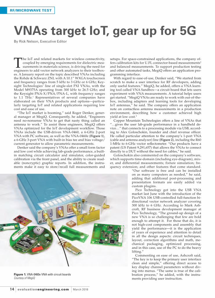
“The IoT market is booming,” said Roger Denker, gener-al manager at MegiQ. Consequently, he added, “Engineers need no-nonsense VNAs to get that nasty thing called an antenna to work.” To assist these engineers, MegiQ offers VNAs optimized for the IoT development workfl ow. Those VNAs include the USB-driven VNA-0460, a 6-GHz 2-port VNA with PC software, as well as the VNA-0460e (Figure 1), a 6-GHz 3-port VNA with built-in bias tee and bias voltage/current generator to allow parametric measurements.
Denker said the company’s VNAs offer a small form factor and low cost while achieving lab-grade performance, a built-in matching circuit calculator and simulator, color-guided calibration via the front panel, and the ability to create read-able (noncryptic) graphic reports. In addition, the instru-ments make it easy to store/recall full measurements and
setups. For space-constrained applications, the company of-fers calibration kits for U.FL connector-based measurements2 and balanced measurements. To support production testing and other automated tasks, MegiQ offers an application pro-gramming interface.
With regard to ease-of-use, Denker said, “We started from scratch to make a user interface for RF developers, adding only useful features.” MegiQ, he added, offers a VNA learn-ing tool called VNA Sandbox—a circuit board that lets users experiment with VNA measurements. A tutorial helps users get started. “MegiQ VNAs are ready to work with out-of-the-box, including adapters and learning tools for developing IoT antennas,” he said. The company offers an application note on contactless antenna measurements in a production environment, describing how a customer achieved high yield at low cost.3
Copper Mountain Technologies offers a line of VNAs that “…gives the user lab-grade performance in a handheld de-vice…” that connects to a processing module via USB, accord-ing to Alex Goloschokin, founder and chief revenue offi cer. He called particular attention to the company’s 1-port VNA (cable and antenna analyzer) line (Figure 2), including the R60 1-MHz to 6-GHz vector refl ectometer. “Our products have a patent (US Patent 9,291,657) that allows the VNAs to connect directly to a DUT without the need for cables,” he said.
Goloschokin also commented on the company’s software, which supports time-domain (including eye-diagram), mix-er, and differential measurements; fixture simulation; fre-quency extension; and other features that come standard.
“Our software is free and can be installed on as many computers as needed,” he said, adding that additional post-processing and presentation formats are easily added via custom plugins.
Pico Technology got into the USB VNA market last June with the introduction of the PicoVNA 106 USB-controlled full-function bi-directional vector network analyzer covering 300 kHz to 6 GHz. According to Mark Ash-croft, RF business development manager at Pico Technology, “The ground-up design of a new VNA is so challenging that few are bold enough to attempt it. For those that do, it is not high-cost components and assembly that yield the performance—it is the application of years of experience and attention to detail in all the design aspects: circuit techniques, layout, correction algorithms and math, me-chanical packaging, optimized processing, and in this case, use of the PC to do the heavy lifting.”
Commenting on ease of use, Ashcroft said, “The key is to keep the primary user interface clean and simple,” offering direct access to key display channel parameters without div-ing into menus. “The same is true of the cali-bration process,” he added, with the instru-ments providing user instruction.
VNAs target IoT, gear up for 5GBy Rick Nelson, Executive Editor
Figure 1. VNA-0460e VNA with circuit boardsCourtesy of MegiQ
14-17_EE_201803_RFMicro_FINAL.indd 1414-17_EE_201803_RFMicro_FINAL.indd 14 2/14/2018 10:08:02 AM2/14/2018 10:08:02 AM

evaluationengineering.comMarch 2018 15
RF/MICROWAVE TEST
He emphasized that ease of use does not come at the expense of established advanced user features and benefi ts. “For example, refer-ence plane shift, de-embedding, all the standard display formats including time domain are all in-cluded,” he said, as is support for unknown-thru calibration, the Touchstone import/export format, and P1dB gain compression.
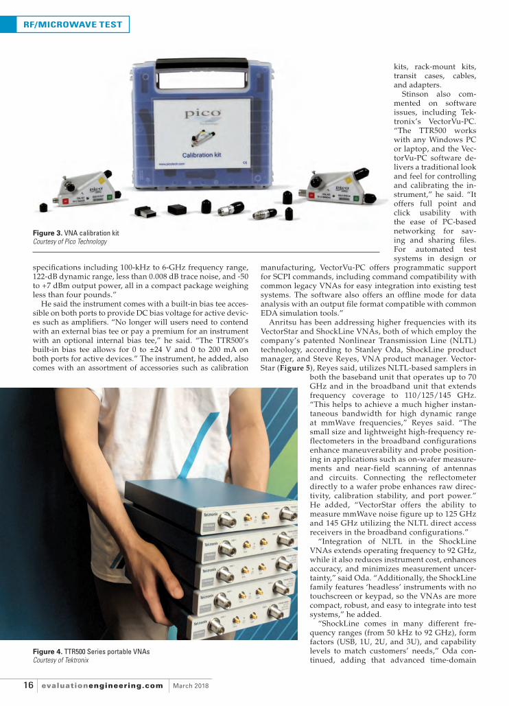
Ashcroft elaborated on calibra-tion. “Essential to any network analysis measurement are the cali-bration (impedance) standards,” he said. “The instrument and its test leads merely have the role of stable transfer standard with no inherent measure-ment accuracy of their own. The standards and the test leads again have typically been very expensive essentials.” Pico, he said, rethought the realization of high-performance calibra-tion standards and offers short, open, load, and thru (SOLT) calibration standards and test leads in both PC3.5 and SMA formats (Figure 3). Residual directivity of typically -50 dB and uncorrected port match of typically -20 dB make the PicoVNA 106 and its premium calibration standards a formidable per-formance combination at low cost, he said.
Ashcroft cited additional applications for VNAs, including dielectric measurements, penetrating radar, and imaging, be it ground, tissues, foods, or engineering materials. “In these arenas, the embedded VNA is increasingly common and the
USB-controlled instrument is ideal,” he said. Similarly, Golos-chokin at Copper Mountain has cited materials testing appli-cations. “Materials testing is a growing application of VNAs, particularly USB VNAs, which can be incorporated into test systems due to their size and portability,” he said.4 He cited interest in an airplane canopy system demonstrated at the company’s booth at last year’s International Microwave Sym-posium in Honolulu.
Tektronix has also recently entered the USB VNA market with the introduction of the TTR500 Series (Figure 4). Dylan Stinson, product manager for RF products at Tektronix, said, “The TTR500 Series offers a full 2-port, 2-path S-parameter VNA for such applications as measuring passive/active components, antennas and matching networks, RF mod-ules, test cables, adapters, and more. It features a solid set of
Figure 2. 1-port VNA (cable and antenna analyzer) line, including the R60 1-MHz to 6-GHz vector refl ectometerCourtesy of Copper Mountain Technologies
Visit www.rsleads.com/803ee-009
USA: +1 (623) 670-5780 | [email protected] EUROPE: +31 (0)180 580 492 | [email protected] WWW.TOP-ELECTRONICSUSA.COM WWW.TOP-ELECTRONICS.COM
Bi-directional with 2 and 3 Port Models
MegiQ VECTOR NETWORK ANALYZER
USB interface and many features, including:
- Sweep up to 20001 points- Measured power range -30 to +5dBm- Port calibrated- Match circuit calculator- Signal Generator output- Bias Voltage/Current generator- VNA-Sandbox (20+ test-circuits & tutorials)
Full size VNA performance in a compact format.
Up to 6 GHzGSM-GPRS-LTE, WiFi, DECT, GPS, ISM, Zigbee, Bluetooth
Affordable & Available Online from
USD3,360.00
14-17_EE_201803_RFMicro_FINAL.indd 1514-17_EE_201803_RFMicro_FINAL.indd 15 2/14/2018 10:07:50 AM2/14/2018 10:07:50 AM
March 2018evaluationengineering.com16
RF/MICROWAVE TEST
specifi cations including 100-kHz to 6-GHz frequency range, 122-dB dynamic range, less than 0.008 dB trace noise, and -50 to +7 dBm output power, all in a compact package weighing less than four pounds.”
He said the instrument comes with a built-in bias tee acces-sible on both ports to provide DC bias voltage for active devic-es such as amplifi ers. “No longer will users need to contend with an external bias tee or pay a premium for an instrument with an optional internal bias tee,” he said. “The TTR500’s built-in bias tee allows for 0 to ±24 V and 0 to 200 mA on both ports for active devices.” The instrument, he added, also comes with an assortment of accessories such as calibration
kits, rack-mount kits, transit cases, cables, and adapters.
Stinson also com-mented on software issues, including Tek-tronix’s VectorVu-PC. “The TTR500 works with any Windows PC or laptop, and the Vec-torVu-PC software de-livers a traditional look and feel for controlling and calibrating the in-strument,” he said. “It offers full point and click usability with the ease of PC-based networking for sav-ing and sharing fi les. For automated test systems in design or
manufacturing, VectorVu-PC offers programmatic support for SCPI commands, including command compatibility with common legacy VNAs for easy integration into existing test systems. The software also offers an offl ine mode for data analysis with an output fi le format compatible with common EDA simulation tools.”
Anritsu has been addressing higher frequencies with its VectorStar and ShockLine VNAs, both of which employ the company’s patented Nonlinear Transmission Line (NLTL) technology, according to Stanley Oda, ShockLine product manager, and Steve Reyes, VNA product manager. Vector-Star (Figure 5), Reyes said, utilizes NLTL-based samplers in
both the baseband unit that operates up to 70 GHz and in the broadband unit that extends frequency coverage to 110/125/145 GHz. “This helps to achieve a much higher instan-taneous bandwidth for high dynamic range at mmWave frequencies,” Reyes said. “The small size and lightweight high-frequency re-flectometers in the broadband configurations enhance maneuverability and probe position-ing in applications such as on-wafer measure-ments and near-field scanning of antennas and circuits. Connecting the reflectometer directly to a wafer probe enhances raw direc-tivity, calibration stability, and port power.” He added, “VectorStar offers the ability to measure mmWave noise figure up to 125 GHz and 145 GHz utilizing the NLTL direct access receivers in the broadband configurations.”
“Integration of NLTL in the ShockLine VNAs extends operating frequency to 92 GHz, while it also reduces instrument cost, enhances accuracy, and minimizes measurement uncer-tainty,” said Oda. “Additionally, the ShockLine family features ‘headless’ instruments with no touchscreen or keypad, so the VNAs are more compact, robust, and easy to integrate into test systems,” he added.
“ShockLine comes in many different fre-quency ranges (from 50 kHz to 92 GHz), form factors (USB, 1U, 2U, and 3U), and capability levels to match customers’ needs,” Oda con-tinued, adding that advanced time-domain
Figure 4. TTR500 Series portable VNAsCourtesy of Tektronix
Figure 3. VNA calibration kitCourtesy of Pico Technology
14-17_EE_201803_RFMicro_FINAL.indd 1614-17_EE_201803_RFMicro_FINAL.indd 16 2/14/2018 10:07:41 AM2/14/2018 10:07:41 AM

evaluationengineering.comMarch 2018 17
RF/MICROWAVE TEST
capabilities, direct-access loops, bias tees, and other options are available to further confi gure ShockLine VNAs for spe-cifi c applications. “For example, the ShockLine MS46522B VNA has an E-band option that brings banded mmWave measurement capabilities to an economic cost level,” he said. “The E-band VNA consists of small tethered source/re-ceiver modules and a base chassis. The modules are attached to the chassis through 1-meter cables that are permanently
Figure 5. VectorStar VNACourtesy of Anritsu
attached to the unit, eliminating the need for any user setup of cables between the VNA and the measure modules. Teth-ered modules connect directly to the DUT for increased mea-surement stability.”
ConclusionAt present, VNAs operating in the 6-GHz range are hitting the sweet spot of IoT designs requiring low-cost, easy-to-use instruments. But as Oda pointed out, the emergence of 5G applications will drive demand for 28 GHz, 39 GHz, and 60 GHz VNAs in 2018 as 5G-related devices gain traction in the marketplace. In addition, he said, VNAs play a vital role in connected-car designs, with radar systems operating at 76 to 81 GHz and infotainment systems operating at high data rates. Finally, Oda said, “Along similar lines, high-speed network systems operating at 100G/400G present an opportunity for VNAs, which can be used to conduct O/E and E/O measurements.” EE
References
1. Nelson, Rick, “IoT, 5G, connected cars drive VNA applications,” EE-Evaluation Engineering, January 2018, p. 6.2. “Using UFL as Test Connectors,” Application Note, MegiQ, 2013. 3. “Using contactless antenna measurement in a production environ-ment,” Application Note, MegiQ, 2016. 4. Nelson, Rick, “CMT founder makes the case for USB vector network analyzers,” Rick’s Blog, EE-Evaluation Engineering Online, July 27, 2017.
Visit www.rsleads.com/803ee-003
Engineering
CONCEPTING PILOT
productionPrototyping
QUALITY PRODUCT
Your Design, Your Way, Quick Qualitywith
DESIGN your custom part in our state-of-the art machine shop DEVELOP a robust process with our
experienced engineering team DELIVER a cost-effective solution from global manufacturing locations
www.Fair-Rite.com I One Commercial Row, Wallkill, NY 12589 I (888) FAIRRITE (324-7748)
14-17_EE_201803_RFMicro_FINAL.indd 1714-17_EE_201803_RFMicro_FINAL.indd 17 2/14/2018 10:07:32 AM2/14/2018 10:07:32 AM

March 2018evaluationengineering.com18
CYBERSECURITY
Testing electronics for faults that occur due to natural phenomena is diffi cult enough; however, what if an anomaly is intentionally introduced? This is the ques-
tion facing the electronics industry. In recent years, the re-search community has delved into the possibility that global outsourcing has made electronics manufacturing too risky. Integrated circuit (IC) manufacturing has attracted the most attention and spawned two major technical conferences—one in the U.S.1 and one in Asia.2 At these forums, researchers addressed the threat of malicious hardware being introduced into an IC—usually referred to as a hardware Trojan. Hard-ware Trojans are designed to evade detection when testing is performed in the traditional manner. When a hardware Trojan in an IC is activated it can make a system inoperable, cause it to malfunction, or even leak sensitive data.
Scoping the threatThe increasing complexity of microcircuits, coupled with fabless manufacturing, have ushered in more possibilities for tiny hardware Trojans to be introduced during an IC’s design or fabrication stages. This almost always leaves post-manufacturing test as the fi nal hope before the device goes into the fi eld. Detecting hardware Trojans at this stage be-comes a vexing problem because we are compelled to ap-ply Shannon’s maxim: “The enemy knows the system.” It was in his 1949 paper “Communication Theory of Secrecy Systems” that Claude Shannon made this assertion; yet, his maxim remains a mainstay for security today. Applying the maxim’s skepticism to hardware Trojans means that we must assume that the attacker knows an IC’s design and the CAD/CAE tools used to create it. We further envision the situation
where the attacker has infi ltrated the process to design the IC, to fabricate it, or both. Only after the IC is manufactured do we assume that the attacker no longer has access to the system to enable a hardware Trojan. A post-manufacturing test, therefore, becomes the remaining obstacle for the at-tacker to overcome. To do this, the attacker calls upon his knowledge of the device’s CAD/CAE tools that include the test vector generation for the IC.
Testing the limits of the testerExhaustive testing is universally acknowledged to be pro-hibitive because even moderately complex designs would take hundreds of years to test so comprehensively. Thus, test generation is an engineering enterprise to balance cost and performance such that tester time is minimized while achiev-ing high fault coverage. Tools for generating test vectors as-sume a fault model. For this article, we apply the commonly-used single stuck-at fault model. In this model the inputs and outputs of an IC’s gates are the fault sites. At these sites, stuck-at faults can occur such that an input or an output is ei-ther stuck-at-0 or stuck-at-1. Although the model only affects inputs and outputs, tests derived for stuck-at faults at those sites are still valid for most physical defects, such as shorts, either on the gate’s inputs or output as well as internal to the gate. The “single” attribute of the fault model stems from the assumption that only a single fault will manifest in the IC. The usefulness of this assumption has been reinforced by evidence showing that tests to detect a single fault in an IC will usually detect multiple, concurrent faults. Equipped with these assumptions, test vector generation can proceed. Next, we show an example of test vector generation that
Simulation for strategic hardware Trojans testingBy Kevin Kwiat, Haloed Sun TEK LLC, and Frank Born, Just Born Tech LLC
Figure 1. Application of binary inputs to an AND gate assigned a stuck-at-1 fault on its output
18-21_EE_201803_CyberSecurity_MECH_KC.indd 1818-21_EE_201803_CyberSecurity_MECH_KC.indd 18 2/9/2018 10:12:42 AM2/9/2018 10:12:42 AM

evaluationengineering.comMarch 2018 19
CYBERSECURITY
yields a set of test vectors having complete single stuck-at fault coverage. Then we show how a knowledgeable attacker can plant a hardware Trojan that evades detection from those test vectors.
An AND gate has inputs A and B and output C. This AND gate can have a test generated for a stuck-at-1 fault (SA1) on its output C (Figure 1).
For the three wires (A, B, and C) associated with this AND gate, fi ve more stuck-at faults remain: C stuck-at-0, A stuck-at-0, A stuck-at-1, B stuck-at-0, and B stuck-at-1. We chose to illus-trate how additional tests can be generated to detect these last three faults (Figure 2).
Table 1 shows all possible input combinations to the AND gate and the single stuck-at-faults detected. Since Table 1 rep-resents exhaustive testing of the AND gate, it is important to ask: what input combinations are needed to test for all single stuck-at faults while minimizing the number of tests? The an-swer is: A=0 and B=1; A=1 and B=0; and A=1 and B=1. These three combinations of inputs test for all possible single stuck-at faults for the AND gate. The test of A = 0 and B = 0 is redundant. Effi ciency compels elimination of this input combination when generating the test set; yet full fault coverage is maintained.
This is precisely the knowledge that the attacker needs. Con-sider the use of the AND gate in a circuit (Figure 3) for perform-ing bus select. However, a hardware Trojan has been added, too. The attacker severed the wire of the AND gate’s output and inserted an XOR gate and connected to it a NOR gate. The XOR gate is the hardware Trojan’s payload and the NOR gate is its trigger. Prior to insertion of the payload and trigger, the cir-cuit, composed only of the AND gate, would raise the BUS-SEL line high only when CTRL and INT are both high (i.e., CTRL=1 and INT=1).
In the presence of the hardware Trojan’s two gates the cir-cuit’s functionality can change dramatically. The payload is triggered when the output of the NOR gate goes high. This causes the XOR gate to invert the AND gate’s attempt to set BUS-SEL low. Instead of BUS-SEL being low, the resultant BUS-SEL signal would go high—creating, as intended by the attack-er, haphazard functionality for the circuit.
We see that the attacker designed the hardware Trojan so that the payload is triggered when the NOR gate’s inputs are both zero (yellow portion of Figure 3). However, notice that this would only occur when the AND gate’s inputs are also both zero. Recall that this is the single input combina-tion that would not be applied to the AND gate using the generated test set.
Fighting through the attackAt this point, we can see that the attacker nefariously used his knowledge of test generation so that the hardware Trojan would not be activated—and hence go undetected—during post-fabrication test. Thus, the attacker achieved his aim: the IC will pass through the testing phase; yet there is an input combination (INT = 1 and CNTL = 1) that will occur in the fi eld causing Trojan activation.
The above scenario underscores that in the realm of out-sourced manufacturing, the testing of incoming ICs for hard-ware Trojans cannot be done in the conventional manner. In the example given, if the seemingly ineffi cient AND gate test of applying zeroes to both its inputs were added to the IC’s test, then the hardware Trojan would have been activated and hence detected. Testing for hardware Trojans calls for augmentation of the tests for the random faults that can oc-cur in an IC. The question becomes, aside from the infeasi-bility of near-exhaustive testing, what augmented test sets should be considered? Since testing is not limited to random faults but directed attacks, strategic considerations must har-ness the decision-making process between an attacker and a tester. Procurers of ICs for critical IC applications such as the power grid, aerospace, military, automotive, health, and fi nance become immersed in this decision-making process when they face the risk of a hardware Trojan. Booz Allen Hamilton, under contract with the Air Force Research Labo-ratory (AFRL), has developed a simulator to make testing for hardware Trojans more plausible and therefore a risk-bal-ancer. The simulator is based on the mathematical discipline of game theory.3 Dr. John Nash (acclaimed in the movie A Beautiful Mind) discovered that applying game theory will always result in states where the opposing players (e.g., the IC procurer and the attacker) have no incentive to deviate from their respective strategies. This is the so-called “Nash equilibrium.” Based on a game theory engine, the simula-tor considers the attacker’s and tester’s strategies and utili-ties (cost and payoffs). It can display the ensuing game in matrix notation (Figure 4) that allows tracking the attacker’s and tester’s possible actions and the accompanying utility of each action. In this matrix, the tester has the possibility of ap-plying different pairings of augmented test sets A, B, C, and D that, under certain probabilities, can detect the presence of various hardware Trojans A, B, C, etc., that an attacker plants with other probabilities. There are more sophisticated hardware Trojans than the example presented here, and more
A B Fault(s) Detected
0 0 C SA1
0 1 C SA1 & A SA1
1 0 C SA1 & B SA1
1 1 A SA0 & B SA0 & C SA0
Table 1. All input combinations for 2-input AND gate and the single stuck-at-faults detected
Figure 2. Testing for three single stuck-at-faults for an AND gate: A stuck-at-1, B stuck-at-0, and B stuck-at-1
18-21_EE_201803_CyberSecurity_MECH_KC.indd 1918-21_EE_201803_CyberSecurity_MECH_KC.indd 19 2/9/2018 10:12:51 AM2/9/2018 10:12:51 AM

March 2018evaluationengineering.com20
CYBERSECURITY
sophisticated testing methods are usually needed to detect them; nonetheless, the simulator is designed to incorporate these other methods of IC testing.
The simulator’s inputs allow applying realistic time and cost limits of testing for hardware Trojans versus the attack-er’s incentives to plant them in an IC. The simulator’s output is an intelligent assessment of the testing resources to be ap-plied and the resultant risk-balancing of the hardware Trojan threat. A cost-benefi t analysis can then be made for IC testing
Figure 4. Screenshot of the hardware Trojan-testing simulator
fl ows that, in addition to testing for traditional faults, also seek to detect hardware Trojans. By applying game theory, procurers of ICs that use the simulator can strategically put their testing resources to use and attain a quantifi able, math-ematically-based balancing of risk.
Most government-developed software can be made avail-able for licensing for commercialization. In fact, this is of-ten in the best interests of the government to ensure that it is properly maintained throughout its life cycle. In many
Figure 3. Hardware Trojan insertion (payload and trigger) in bus select circuit
18-21_EE_201803_CyberSecurity_MECH_KC.indd 2018-21_EE_201803_CyberSecurity_MECH_KC.indd 20 2/9/2018 10:13:01 AM2/9/2018 10:13:01 AM
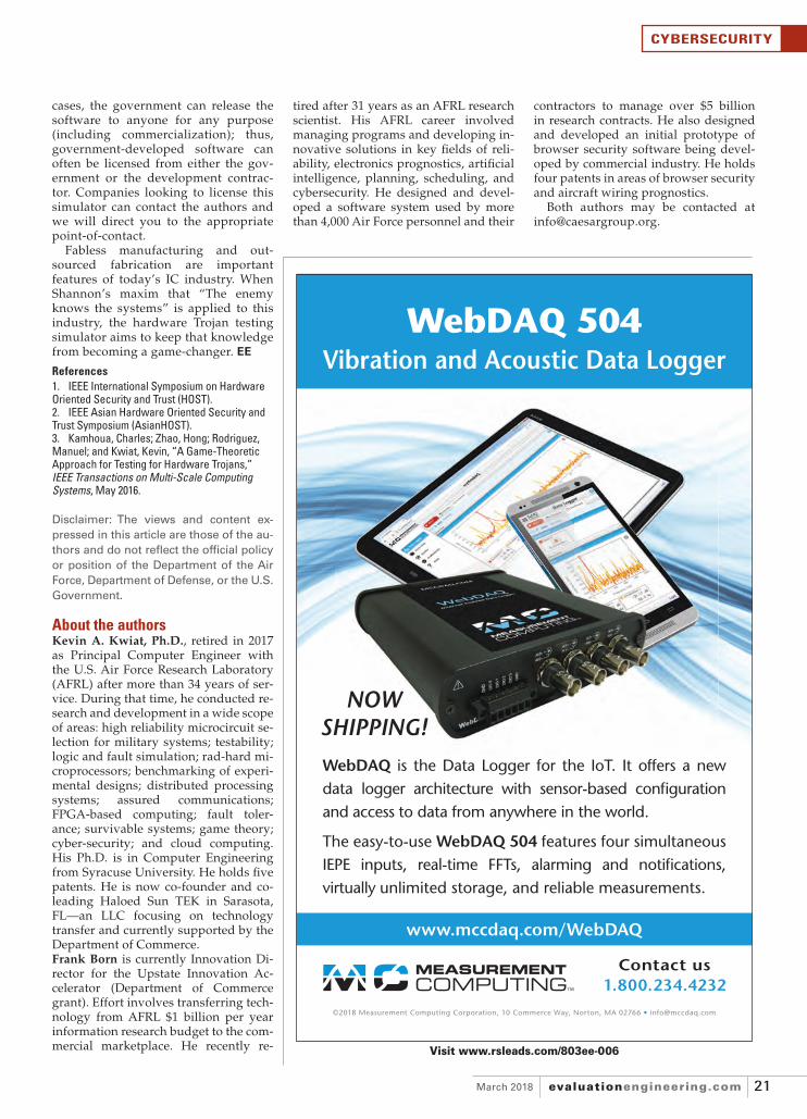
evaluationengineering.comMarch 2018 21
CYBERSECURITY
©2018 Measurement Computing Corporation, 10 Commerce Way, Norton, MA 02766 • [email protected]
Contact us1.800.234.4232
WebDAQ 504Vibration and Acoustic Data Logger
WebDAQ is the Data Logger for the IoT. It offers a new data logger architecture with sensor-based confi guration and access to data from anywhere in the world.
The easy-to-use WebDAQ 504 features four simultaneous IEPE inputs, real-time FFTs, alarming and notifi cations, virtually unlimited storage, and reliable measurements.
www.mccdaq.com/WebDAQ
NOW SHIPPING!
Visit www.rsleads.com/803ee-006
cases, the government can release the software to anyone for any purpose (including commercialization); thus, government-developed software can often be licensed from either the gov-ernment or the development contrac-tor. Companies looking to license this simulator can contact the authors and we will direct you to the appropriate point-of-contact.
Fabless manufacturing and out-sourced fabrication are important features of today’s IC industry. When Shannon’s maxim that “The enemy knows the systems” is applied to this industry, the hardware Trojan testing simulator aims to keep that knowledge from becoming a game-changer. EE
References
1. IEEE International Symposium on Hardware Oriented Security and Trust (HOST). 2. IEEE Asian Hardware Oriented Security and Trust Symposium (AsianHOST). 3. Kamhoua, Charles; Zhao, Hong; Rodriguez, Manuel; and Kwiat, Kevin, “A Game-Theoretic Approach for Testing for Hardware Trojans,” IEEE Transactions on Multi-Scale Computing Systems, May 2016.
Disclaimer: The views and content ex-
pressed in this article are those of the au-
thors and do not refl ect the offi cial policy
or position of the Department of the Air
Force, Department of Defense, or the U.S.
Government.
About the authorsKevin A. Kwiat, Ph.D., retired in 2017 as Principal Computer Engineer with the U.S. Air Force Research Laboratory (AFRL) after more than 34 years of ser-vice. During that time, he conducted re-search and development in a wide scope of areas: high reliability microcircuit se-lection for military systems; testability; logic and fault simulation; rad-hard mi-croprocessors; benchmarking of experi-mental designs; distributed processing systems; assured communications; FPGA-based computing; fault toler-ance; survivable systems; game theory; cyber-security; and cloud computing. His Ph.D. is in Computer Engineering from Syracuse University. He holds fi ve patents. He is now co-founder and co-leading Haloed Sun TEK in Sarasota, FL—an LLC focusing on technology transfer and currently supported by the Department of Commerce.Frank Born is currently Innovation Di-rector for the Upstate Innovation Ac-celerator (Department of Commerce grant). Effort involves transferring tech-nology from AFRL $1 billion per year information research budget to the com-mercial marketplace. He recently re-
tired after 31 years as an AFRL research scientist. His AFRL career involved managing programs and developing in-novative solutions in key fi elds of reli-ability, electronics prognostics, artifi cial intelligence, planning, scheduling, and cybersecurity. He designed and devel-oped a software system used by more than 4,000 Air Force personnel and their
contractors to manage over $5 billion in research contracts. He also designed and developed an initial prototype of browser security software being devel-oped by commercial industry. He holds four patents in areas of browser security and aircraft wiring prognostics.
Both authors may be contacted at [email protected].
18-21_EE_201803_CyberSecurity_MECH_KC.indd 2118-21_EE_201803_CyberSecurity_MECH_KC.indd 21 2/9/2018 10:13:10 AM2/9/2018 10:13:10 AM

March 2018evaluationengineering.com22
INDUSTRYHAPPENINGS
By Rick Nelson, Executive Editor
The International Electron Devices Meeting (IEDM) held Dec. 2-6, 2017, in San Francisco offered imec and
Leti an opportunity to disclose several innovations. imec announced three new developments: ultralow contact resistivity of 5x10⁻¹⁰ Ωcm2 for gallium (Ga)-doped p-germanium (Ge) source/drain contacts, multiple key process optimizations for vertically stacked gate-all-around (GAA) silicon nanowire transistors, and a pow-er-performance-area-cost (PPAC) analy-sis of different sequential 3D-integration variants using advanced 5-nm and 3-nm CMOS technology nodes. Leti, a research institute of CEA Tech, demonstrated signif-icant improvements in the fi eld of memory systems and announced it has integrated hybrid III-V silicon lasers on 200-mm wa-fers using a standard CMOS process fl ow.
Ultralow contact resistivityimec said its results, with regard to ultralow contact resistivity, are important in light of further downscaling of the CMOS source/drain contact area, which is challenged by a parasitic source/drain resistance that re-sults in suboptimal transistor functioning. The low contact resistivity and high level
IEDM sees transistor, memory, laser innovations
of Ga activation were achieved after nano-second laser activation (NLA) at low ther-mal budget. The results show that highly Ga-doped Ge-rich source/drain contacts provide a promising route for suppressing parasitic source/drain resistance in ad-vanced pMOS devices.
High dopant activation is known to be an attractive approach for lowering source/drain contact resistance, imec said. Traditionally in pMOS devices, Si source/drain contacts with high boron (B) activa-tion are used. But in more advanced pMOS devices, Ge- and SiGe(Sn)-based source/drain contacts are a promising alterna-tive since they introduce benefi cial strain. However, the higher the Ge content, the lower the boron activation and solubility in Ge or Ge-rich SiGe.
The new fi ndings result from a compre-hensive study of Ga dopant activation in Si, Si0.4Ge0.6, and Ge conducted by imec, KU Leuven (Belgium), and Fudan Univer-sity (Shangai, China). In this study, either rapid thermal annealing (RTA) or Applied Materials’ Nanosecond Laser Activation (NLA) were used as dopant activation technologies, after Ga ion implantation. imec reported that the record low contact
resistivity of 5x10⁻¹⁰ Ωcm2 and a high dop-ant activation level of 5x1020 cm-3 were obtained for Ga-doped Ge source/drain contacts after NLA. The low contact resis-tivity can be attributed to a benefi cial Ge/Ga surface aggregation following the NLA process. With RTA activation at 400°C, a contact resistivity as low as 1.2x10⁻⁹ Ωcm2
was reported. The study shows that Ga might be preferred over B as a dopant for Ge or high-Ge content source/drain con-tacts in pMOS devices.
“For the fi rst time, we have achieved contact resistivities far below 10-9 Ωcm2 for high-Ge content source/drain contacts,” said Naoto Horiguchi, distinguished member of the technical staff at imec, in a press release. “This proves that Ga dop-ing and activation by NLA or RTA are an attractive alternative to boron doping for these source/drain contacts. It provides a possible path for further performance improvement using the current source/drain schemes in next-generation technol-ogy nodes.”
The results were obtained at low ther-mal budget activation, making Ga doping particularly attractive for devices that re-quire low-thermal budget processing.
GAA MOSFETsGAA MOSFETs based on vertically stacked horizontal nanowires or nanosheets are promising candidates to succeed FinFETs in sub-5-nm technology nodes, thus ex-tending today’s CMOS technology be-yond its scaling limits, imec said, adding that this innovative transistor architecture offers more aggressive gate-pitch scaling than FinFETs because it achieves a better electrostatic control. Moreover, in highly scaled standard cells where only one fi n device is allowed, nanosheets provide more current per footprint than fi ns and thus can drive higher capacitive loads. Fi-nally, integrating nanosheet devices with variable widths in a single platform en-ables power/performance optimization with high granularity.
As with every disruptive innovation, this new architecture demands process optimizations, imec said. At IEDM, a team of researchers from imec and Applied Ma-terials demonstrated multiple optimiza-tions for the fabrication of stacked silicon nanowire and nanosheet FETs. The fi rst process optimization is the implementa-tion of SiN shallow trench isolation (STI)
Figure 1. Ring oscillator gate delay versus VDD for stacked silicon nanowire FETsCourtesy of imec
22-24_EE_201803_IndHappenings_MECH_KC.indd 2222-24_EE_201803_IndHappenings_MECH_KC.indd 22 2/9/2018 3:34:41 PM2/9/2018 3:34:41 PM

evaluationengineering.comMarch 2018 23
liners that suppress oxidation-induced fi n deformation and improve the shape con-trol of the nanowire or nanosheet. Second, Applied Materials’ Selectra Etch was used to enable nanowire/nanosheet release and inner spacer cavity formation with high selectivity and without causing silicon re-fl ow. Finally, for the fi rst time, ring oscilla-tor circuits were reported based on stacked silicon nanowire FETs, including dual work function metal gates for threshold voltage control. Figure 1 shows ring oscil-lator gate delay versus V
DD for stacked sili-
con nanowire FETs. The gate delay reduces with increasing V
DD and with decreasing
LG, confi rming ring oscillator functionality.imec also presented a study on the reli-
ability of GAA nanowires, showing that the degradation mechanisms and their origins are similar to the one in planar devices. The modeling of the degrada-tion including various channel hot-carrier (CHC) modes as well as positive bias temperature instability (PBTI) allows an extrapolation to 10-year lifetime in the full bias space. The obtained safe operation area (SOA) was used to optimize device operation. An extra degradation mecha-nism that must be taken into account is self-heating, which is important in such confi ned structures. Finally, in a study on ESD diodes in sub-7-nm GAA nanowire technology nodes, imec proved that the diodes’ performance is signifi cantly im-pacted by some of the process options and that optimizations are needed, such as a wraparound contact (WAC) that can increase contact area in a scaled fi n pitch and can be combined with GAA.
“GAA nanowire transistors are key in further CMOS scaling,” stated Horigu-chi. “Earlier this year, we demonstrated standalone transistors and CMOS integra-tion; now the next step was taken with a full demonstrator, showing the enormous promise this technology holds for realiz-ing the sub-7-nm technology nodes.”
PPAC analysis of 3D variantsFinally at IEDM, imec presented what it called the fi rst PPAC analysis of different sequential 3D-integration variants using advanced 5-nm and 3-nm CMOS technol-ogy nodes. The most signifi cant benefi t was found for a heterogeneous sequen-tial-3D integration approach that uses different device layers (or tiers) for the nonscalable (analog and I/O) and scal-able parts (logic and memory) of the sys-tem. These results confi rm the potential of heterogeneous sequential-3D integra-tion as a possible route for heterogeneous scaling—an emerging approach that inte-grates multiple transistor architectures in one system-on-chip.
Sequential-3D integration (S3D) is widely viewed as a promising alternative to continue the benefi ts offered by semi-conductor scaling, imec said. S3D involves the vertical integration of sequentially pro-cessed device layers (or tiers) with isola-tion and interconnect layers in between. Three levels of granularity can be defi ned, depending on where the partitioning and stacking take place: at the transistor level (T-S3D), cell level (C-S3D), or IP block lev-el, also called heterogeneous S3D (H-S3D). H-S3D is considered as a possible enabler for heterogeneous scaling. Compared with traditional through-Si-via (TSV)-based 3D-integration techniques, S3D in general offers a higher interconnect density and a more precise (lithography-defi ned) align-ment of the stacked transistors, cells, and IP blocks.
imec said that for the fi rst time ever, it has quantifi ed the PPAC benefi ts of the various S3D variants for 5-nm and 3-nm technology nodes. To meet the challenges for S3D fabrication, the imec team used advanced technologies in some of the most critical process steps. The largest PPAC benefi t was found for a heterogenous S3D use case, where the logic and memory part is scaled to iN5 technology, and the remaining nonscalable part (analog and
I/O) is manufactured in N28 technology in the top tier. For this use case, despite a high wafer cost, a die cost reduction of 33% was achieved with respect to a 2D-SoC imple-mentation with 125-mm2 die size.
“Our results demonstrate the poten-tial of S3D technology, which benefi ts the implementation of next-generation appli-cation hardware such as 5G and artifi cal intelligence,” said Nadine Collaert, dis-tinguished member of the technical staff at imec.
imec said its research into advanced logic scaling is performed in cooperation with imec’s key CMOS program partners, including GlobalFoundries, Huawei, Intel, Micron, Qualcomm, Samsung, SanDisk/Western Digital, SK Hynix, Sony Semiconductor Solutions, Toshiba Memory, and TSMC.
Memory system improvementsLeti at IEDM demonstrated signifi cant improvements in the fi eld of memory sys-tems, including reconfi guring SRAM into content-addressable memory (CAM), im-proving nonvolatile crossbar memories, and using advanced tunnel fi eld-effect transistors (TFET). The organization also presented a high-density SRAM bitcell on Leti’s CoolCube 3D platform, which
Figure 2. Tilted scanning electron microscopy view of the III-V/Si DFB laser after the III-V patterning steps.Courtesy of Leti
22-24_EE_201803_IndHappenings_MECH_KC.indd 2322-24_EE_201803_IndHappenings_MECH_KC.indd 23 2/9/2018 3:34:55 PM2/9/2018 3:34:55 PM

March 2018evaluationengineering.com24
INDUSTRYHAPPENINGS
reduces the area required for memory by 30% while maintaining full device func-tionality. This breakthrough points the way to easing the major memory bottleneck in more complex systems on chip, Leti said, where up to 90% of the SoC area might be taken by SRAM. The breakthroughs were reported Dec. 5 at IEDM 2017 in a paper titled “Advanced Memory Solutions for Emerging Circuits and Systems.”
A key obstacle to shrinking SRAM on SoCs is bitcell-area limitations linked to required performance and yield, both of which become more challenging as tech-nology scales, Leti said. Lowering system power consumption is also limited by memory, as the SRAM performance and its stability scale less successfully than logic performance at lower voltages. Oth-er memories like CAM might be affected even more by voltage scaling.
“All of these obstacles become particu-larly important for the Internet of Things, where ultralow-power consumption and the cost of individual nodes are crucial, and SRAM limitations have a big impact on both,” said Bastien Giraud, one of the paper authors, in a press release.
Leti approached these challenges with a CoolCube SRAM design focusing on the development of a compact and functional four-transistor bitcell, along with other in-novations:•reconfi guring memory between the CAM and SRAM, depending on the ap-plication;•optimizing memory using TFET, fo-cusing on the exploitation of its nega-tive differential-resistance effect to build ultralow-power SRAM, fl ip-fl ops, and refresh-free DRAM; and
Figure 3. Laser spectrum for 160-mA injection currentsCourtesy of Leti
•a new compensation technique for crosspoint memory that reduces the voltage drop and leads to larger memory arrays.
Leti said its proposed CAM/SRAM out-performs state-of-the-art memories, with operations at 1.56 GHz and 0.13-fJ/bit en-ergy per search. In addition, the proposed TFET designs are competitive in terms of area, performance, and static power consumption. Leti’s proposed compensa-tion technique in crosspoint memory also enables the design of cost-effi cient large memory arrays, while reducing the impact of temporal and spatial variations.
Short-term applications include cross-bar circuits for storage-class memory and fl exible SOCs with SRAM/CAM reconfi gurability. “In the longer term, Leti’s CoolCube technology will be able to deliver very high-density SRAM,” Gi-raud said. “Enabling TFET-based DRAM and integrating TFET standard cells into CMOS designs will allow circuit design-ers to take advantage of the best features of both technologies.”
Hybrid III-V silicon lasersLeti also reported at IEDM that it has in-tegrated hybrid III-V silicon lasers on 200-mm wafers using a standard CMOS process fl ow. This breakthrough shows the way to transitioning away from 100-mm wafers and a process based on bulk III-V technology that requires contacts with noble metals and lift-off-based patterning.
The project, carried out in the frame-work of the IRT Nanoelec program, which is headed by Leti, demonstrated that the hybrid device’s performance is compara-ble to the reference device fabricated with the current process on 100-mm wafers.
The fabrication fl ow is fully planar and compatible with large-scale integration on silicon-photonic circuits. The results were reported Dec. 5 at IEDM 2017 in a paper titled “Hybrid III-V/Si DFB Laser Integration on a 200-mm Fully CMOS-compatible Silicon Photonics Platform.”
CMOS compatibility with silicon pho-tonics lowers fabrication costs and pro-vides access to mature and large-scale facilities, which enables packaging com-patibility with CMOS driving circuits, Leti said.
“Silicon-photonic technologies are becoming more mature, but the main limitation of these platforms is the lack of an integrated light source,” said Ber-trand Szelag, a coauthor of the paper. “This project showed that a laser can be integrated on a mature silicon-photonic platform with a modular approach that does not compromise baseline process performances. We demonstrated that the entire process can be done in a standard CMOS fabrication line with conven-tional processes and materials, and that it is possible to integrate all the photonic building blocks at large scale.”
The integration required managing a thick silicon fi lm, typically 500 nm thick, for the hybrid laser, and a thinner one, typically 300 nm, for the baseline silicon-photonic platform. The integration re-quired locally thickening the silicon by adding 200 nm of amorphous silicon via a damascene process, which presents the advantage of leaving a fl at surface favor-able for bonding III-V silicon. The laser can be integrated on a mature silicon pho-tonic platform with a modular approach that does not compromise the baseline process performance. Figure 2 shows a tilted scanning electron microscopy view of the III-V/Si distributed feedback (DFB) laser after the III-V patterning steps. Fig-ure 3 shows the laser spectrum for 160-mA injection currents
The novelty of the approach also includ-ed using innovative laser electrical contacts that do not contain any noble metals, such as gold. The contacts also prohibit integra-tion lift-off-based processes. Nickel-based metallization was used with an integration technique similar to a CMOS transistor technique, in which tungsten plugs con-nect the device to the routing metal lines.
Next steps include integrating the laser with active silicon-photonic devices—for example, a modulator and photodiode with several interconnect metal levels in a planarized backend. Finally, III-V die bonding will replace III-V wafer bonding in order to process lasers on the entire sili-con wafer. EE
22-24_EE_201803_IndHappenings_MECH_KC.indd 2422-24_EE_201803_IndHappenings_MECH_KC.indd 24 2/9/2018 3:35:43 PM2/9/2018 3:35:43 PM

EE201803_AD HOUSE.indd 25EE201803_AD HOUSE.indd 25 2/8/2018 3:36:06 PM2/8/2018 3:36:06 PM

March 2018evaluationengineering.com26
INDUSTRYHAPPENINGS
By Rick Nelson, Executive Editor
DesignCon, held Jan. 31 to Feb. 1 in Santa Clara, provided companies an opportunity to highlight their
products and technologies for high-speed digital-communications applications. Rel-evant products from DesignCon exhibi-tors including ANSYS, Cadence Design Systems, Keysight Technologies, Molex, National Instruments, Rohde & Schwarz, and Tektronix were highlighted in our January Special Report on high-speed digital design, interconnect, and test.1 In the runup to and during the event, com-panies have reported additional capabili-ties related to IP, components, intercon-nect, and test and measurement.
Leading up to the event, Rambus Inc. announced its GDDR6 (Graphics Double Data Rate) Memory PHY IP Core targeted for high-performance applications including cryptocurrency mining, AI, ADAS, and networking. Leveraging almost 30 years of high-speed interface design expertise and using advanced leading-edge FinFET process nodes, the company reported, the Rambus GDDR6 PHY architecture will provide speeds of up to 16 Gb/s while utilizing established packaging and testing techniques.
“The high bandwidth delivered by GDDR6 makes it uniquely qualified to perform data-intensive applications such as HPC, AI, autonomous ve-hicles, and high-speed networking,” said Luc Seraphin, senior vice presi-
dent and general manager of the Ram-bus Memory and Interfaces Division, in a press release. “We are excited to be the first IP provider to offer a GDDR6 PHY solution with industry-leading performance designed with power ef-ficiency and high signal margins for these applications.”
PCIe compliance solutionAnritsu at DesignCon reported that its MP1900A Signal Quality Analyzer-R (SQA-R) has been certified as a com-pliance test solution for PCI Express (PCIe) 3.0 technology Link Equaliza-tion (Link EQ) tests and Receiver (Rx) Jitter Tolerance tests by the PCI-SIG consortium. With support for the PCI Express 3.0 specification, as well as expandability to PCI Express 4.0 and 5.0 specifications, the MP1900A helps control capital equipment expenses while supporting various tests, such as PHY layer electrical characteristics and protocol tests, using a high-qual-ity waveform pulse pattern generator (PPG) and high-sensitivity error de-tector (ED), the company reported.
Anritsu describes the MP1900A SQA-R (Figure 1) as a multichannel bit-error-rate tester (BERT) offering high-level, high-waveform-quality PPG with 115-fs intrinsic jitter, high-accuracy jitter generation sources (SJ, RJ, SSC, and BUJ), and a noise source for generating CM-I/DM-I/white
noise. The instrument has a 15-mV high-input-sensitivity error detec-tor (ED) with embedded clock recov-ery, allowing accurate BER tests to be made, even with a very small closed eye.
The certified test solution integrates the MP1900A SQA-R with the Tele-dyne LeCroy SDA830Zi-B serial data analyzer, which has up to 30 GHz of bandwidth and an 80-GS/s sample rate. Engineers can use the integrated solution to perform calibration for evaluating the PHY layer of PCI Ex-press 3.0 (8 GT/s) technology add-in cards and system boards, as well as Link EQ tests for verification of the device-under-test communications state. Rx tests to measure the DUT stress tolerance can be performed, as well. Using the SQA-R and SDA830Zi-B supports high-repeatability testing, as well as troubleshooting analysis. In-clusion of the Teledyne LeCroy instru-ment also allows support for transmis-sion-side tests.
Clock recovery and signal integrityKeysight Technologies demonstrated several new capabilities at Design-Con, including the new N1076B 16/32/64-Gbaud Electrical Clock Re-covery Solution for analysis of PAM4 designs as defi ned in emerging stan-dards such as IEEE 802.3bs/cd and OIF-CEI-56G/112G. The company also demonstrated EEsof ADS 2017 signal-integrity channel simulation combined with N8844A data-analytics software to quickly and easily compare simulation results with measured data.
The company also reported that its Physical Layer Test System (PLTS) 2017, including the addition of PAM4 eye dia-gram testing, offers signifi cant capabili-ties with regard to manufacturing test of high-speed interconnects. Furthermore, the company said, the new S93011A PNA-TDR software offers digital signal-integrity engineers a one-box solution for characterizing high-speed serial in-terconnects. In addition, Keysight said its EEsof ADS 2017 includes a new Elec-troThermal simulator for PIPro, which provides a complete solution for the power integrity (PI) workfl ow, such as DC IR drop, DC electrothermal, and PDN impedance analysis.
Figure 1. MP1900A Signal Quality Analyzer-R (SQA-R) multichannel bit-error-rate testerCourtesy of Anritsu
DesignCon highlights IP and interconnect as well as test and measurement
22-24_EE_201803_IndHappenings_MECH_KC.indd 2622-24_EE_201803_IndHappenings_MECH_KC.indd 26 2/9/2018 3:36:52 PM2/9/2018 3:36:52 PM

evaluationengineering.comMarch 2018 27
ConnectivityTE Connectivity reported that it show-cased OSFP and QSFP-DD connectivity products that will soon enable 400 Gigabit Ethernet in a range of datacenter devices. Targeted for massive aggregation of data across an array of applications, 400 Giga-bit Ethernet (GbE) has completed the stan-dardization process and was published in December 2017 by the IEEE 802.3bs Ether-net Working Group. Development of new and faster electrical and optical signaling technologies is simultaneously underway across the ever-expanding Ethernet eco-system, the company said.
TE described the QSFP form factor as today’s industry workhorse for deliver-ing 40 and 100 GbE. The Q is for quad—a nod to the four-channel electrical inter-face, with each lane running at 25 Gb/s for 100 GbE, the company explained. TE’s QSFP-DD connector adopts the same ba-sic concept as its predecessor, but doubles the electrical contact density, via eight dif-ferential pairs capable of 50 Gb/s each, to achieve 400 GbE while allowing ex-isting QSFP modules to be plugged into the same cage. The OSFP form factor is designed for maximum thermal and elec-trical performance but does not provide backwards compatibility to existing form factors without an adapter. The O is for octal—it is being designed to use eight electrical lanes to deliver 400 GbE—and SFP is for “small form factor pluggable.”
In addition, TE and Credo Semi-conductor, a provider of mixed-signal semiconductors for the datacenter, en-terprise-networking, and high-perfor-mance-computing markets, announced they had teamed up to demonstrate 112 Gb/s over a chip-to-module I/O chan-nel and over a backplane channel. The demonstration employed TE’s OSFP I/O connector operating over a 10-inch PCB channel. The channel was driven by Cre-do’s 16-nm 112G PAM4 SerDes, operating over a total ball-to-ball channel loss of >15 dB. The demo showed bit error rate (BER) performance of better than 1x10⁻⁷.
High-speed connectorAlso addressing interconnect at Design-Con was Molex. The company high-lighted products such as the Impulse orthogonal direct backplane connector system and BiPass I/O and backplane cable assemblies, predicted in our Janu-ary article.1 In addition, Molex reported that it highlighted its NearStack high-speed connector system and cable jumper assemblies (Figure 2), which use twinax cables to deliver a PCB alternative with superior signal integrity and low inser-
tion loss while enabling implementation of 56 Gb/s NRZ and a path to 112 Gb/s PAM4.
The company also showcased its Impel Plus cabling system, emphasiz-ing its backbone functionality within the Open19 Project,2 which defi nes a common form factor for servers, Tier-0 switches, and power shelves with a base internal cage system that can be imple-mented into a standard 19” rack solu-tion. Delivering lower costs and reliable signal integrity from the switch to serv-er with a robust connector to cable inter-face, the Molex Impel Plus cabling sys-tem achieves data rates up to 50 Gb/s PAM4 to create 100-Gb/s connectivity per server with the Open19 solution, the company reported.
In addition, Molex highlighted its high-density blind-mating optical back-plane connectors for card, sled, and drawer applications that incorporate multifi ber MT and VersaBeam expand-ed-beam MT ferrule technology, en-abling the deployment of optical I/O based hardware. By utilizing Molex FlexPlane and Routed Ribbon solutions, system architects are able to manage onboard optical fi ber counts that range from hundreds to thousands of fi bers, the company reported.
Engineering awardFinally, DesignCon organizers announced the winner of the event’s Engineer of the Year Award: Dr. Mike Peng Li, Intel Fel-low and the technologist for high-speed I/O and interconnects in the Program-mable Solutions Group at Intel Corp. The Engineer of the Year Award recognizes
elite ability and accomplishments in engi-neering and new product advancements at the chip, board, or system level, with a special emphasis on signal integrity and power integrity. As this year’s winner, DesignCon will bestow a $10,000 grant to the educational institution of Dr. Li’s choice in his name. The award was pre-sented on Thursday, Feb. 1, at DesignCon.
“The Engineer of the Year Award rec-ognizes an individual who has made substantial contributions to the fi eld of engineering, and we are happy to rec-ognize Dr. Mike Peng Li for his lifelong commitment to supporting innovation and discovery in this fi eld,” said Nao-mi Price, conference content director at UBM, the event organizer. “Throughout his illustrious career, Dr. Li has continu-ally pushed the envelope on industry standards across multiple topics, in-cluding Ethernet and PCI Express, and is an extremely deserving recipient of this award.”
“DesignCon has emerged as one of the primary technical conferences on signal integrity and high-speed I/O for chips, boards, and systems over the years and I am honored to receive such acknowl-edgement,” said Dr. Li.
The DesignCon 2019 conference is scheduled for Jan. 29-31, 2019, in Santa Clara, with the exposition being held Jan. 30-31. EE
References
1. Nelson, Rick, “Software and instruments chase blazingly fast signals,” EE-Evaluation Engineering, Jan. 20, 2018, p. 12. 2. Bachar, Yuval, “Open19 in 2018,” Open19 Foundation, Jan. 17, 2018.
Figure 2. NearStack high-speed connector systemCourtesy of Molex
22-24_EE_201803_IndHappenings_MECH_KC.indd 2722-24_EE_201803_IndHappenings_MECH_KC.indd 27 2/9/2018 3:37:09 PM2/9/2018 3:37:09 PM
March 2018evaluationengineering.com28
POWER SEMICONDUCTORS PRODUCT FOCUS
Power transistors, drivers, controllers energize diverse array of productsBy Rick Nelson, Executive Editor
The Special Report on page 6 of this issue covers power supplies and loads and also offers coverage of
products and technologies expected to be highlighted at APEC 2018, March 4-8 in San Antonio, TX. This Product Focus takes a look at some of the transistors, controller ICs, and evaluation boards that can help you effi ciently power today’s applications.
Of note is a series of silicon-carbide (SiC) MOSFETs, the latest addition to Littelfuse’s power-semiconductor line. The devices result from what the company describes as an incremental step toward establishing itself in the power-semiconductor industry through taking a majority investment in the SiC development company Monolith Semiconductor last March. The LSIC1MO120E0080 Series is the fi rst organically designed, developed, and manufactured SiC MOSFET to be released by this partnership.
“Our new SiC MOSFET Series is a critical milestone in our journey to become a leading component supplier in the power semiconductor industry,” said Michael Ketterer, product marketing manager for power semiconductors at Littelfuse. “Our SiC MOSFET application support network is prepared to help customers enhance the performance of their existing designs, as well as assist those developing new power converter products.” Typical applications for these new SiC MOSFETs include power-conversion
systems such as solar inverters, switch-mode power supplies, UPS systems, motor drives, high-voltage DC/DC converters, battery chargers, and induction heating.
Other application areas for the products described below range from automotive to consumer electronics. Addressing the latter is an LLC controller from Texas Instruments. “The consumer electronics market demands effi cient power supplies with low standby power. With this new family of LLC controllers, TI is enabling designers to do more with less power,” said Steve Lambouses, TI vice president, High Voltage Power. “The UCC256301 was designed to meet tomorrow’s power requirements by delivering breakthroughs in standby power and effi ciency while simplifying design and lowering system cost.”
For automotive applications, Melexis has announced new fan driver ICs. “Cooling has always been an enabler for innovation,” Dirk Leman, fan drivers product line manager, said. “As more electronics are integrated into cars, there is a growing need for automotive fans. These new drivers from Melexis ensure that the fans can be driven quietly and reliably, which consumers expect for in-cabin applications. As these automotive-grade devices are fully integrated with no external components required, it is now possible to utilize the benefi ts of soft switching in the smallest fan applications.”
LLC resonant controllerThe UCC256301 inductor-inductor-capacitor (LLC) resonant
controller with an integrated high-voltage gate driver enables
the industry’s lowest standby power as well as longer system
lifetimes, the vendor reports, adding that the UCC256301 pro-
vides a cost-effective system solution that helps meet stringent
energy-effi ciency standards for a range of AC/DC applications,
including digital televisions, gaming adapters, desktop com-
puters and notebook adapters, and power-tool battery char-
gers. The UCC256301 enables standby power of less than 40
mW when fully regulating the system output.
By achieving a new low in standby power, the controller
exceeds European Code of Conduct (CoC) Tier 2 and U.S. De-
partment of Energy (DoE) Level VI effi ciency standards and
achieves more than 90% effi ciency with a 10% load, the com-
pany reports. Hybrid hysteretic control, a new patented con-
trol method, enables up to 10 times faster transient response
and reduces output capacitance by 20%. Texas Instruments, www.rsleads.com/803ee-183
IMS evaluation platformThe Insulated Metal Substrate (IMS) Evaluation Platform pro-
vides a fl exible, low-cost, high-power development platform
for high-effi ciency power systems with 3-kW or higher ap-
plications. The IMS Evaluation Platform, in combination with
GaNPX packaging technology and smart design techniques,
enables power engineers to quickly take full advantage of
GaN power transistors in designing smaller, lighter, lower
cost, and more effi cient power systems for datacenter, auto-
motive, and energy-storage system applications.
This evaluation platform consists of a motherboard
(GSP65MB-EVB) and two IMS evaluation modules in half-
bridge and full-bridge variants. The modules can be confi g-
ured as a half-bridge (single IMS module) or a full bridge
(two IMS modules) on the high-power motherboard. IMS
evaluation modules are available in two power levels: 3
kW and 6 kW. The IMS evaluation module includes GaN E-
HEMTs, gate drivers, isolated DC/DC supply, DC bus decou-
pling capacitors, and a heatsink to form a fully functional
half-bridge power stage.
Platform benefi ts include low thermal resistance and an
optimized layout. The drive board is tightly coupled with
the IMS board to minimize power commutation and gate-
driver loops to optimize performance. GaN Systems, www.rsleads.com/803ee-184
28-29_EE_201803_ProdFocus_MECH_KC.indd 2828-29_EE_201803_ProdFocus_MECH_KC.indd 28 2/8/2018 3:43:00 PM2/8/2018 3:43:00 PM

evaluationengineering.comMarch 2018 29
POWER SEMICONDUCTORS PRODUCT FOCUS
Automotive-grade fan driver ICsThe US168KLD and US169KLD
are automotive grade single-chip
solutions for driving single-coil
brushless DC fans and motors.
As a result of their soft-switching
characteristics, they ensure low
levels of EMI and acoustic noise,
making them suitable for in-cab-
in automotive applications such
as sensor fans as well as other
applications such as cooling fans for wireless chargers, com-
puting, audio, and multimedia.
Confi gured as a full-bridge driver with the ability to drive
motor currents up to 300 mA and a supply range from 1.8 V
to 5 V, the devices include a sensitive integrated Hall-effect
sensor. Built-in reverse voltage, locked rotor, and thermal
protection ensure that the drivers are robust, even in chal-
lenging applications.
These fan drivers will be qualifi ed to AEC-Q100, ensuring
that they are reliable in the most stringent applications.
Melexis, www.rsleads.com/803ee-185
750-W CW RF transistorThe MRF13750H/MRF13750HS RF power LDMOS transistors,
available in bolt-down and solder-down styles, are 750-W con-
tinuous-wave transistors designed for industrial, scientifi c, and
medical (ISM) applications in the 700- to 1,300-MHz frequency
range. They are capable of CW or pulse power in narrowband
operations.
The transistors are internally input-matched, can be used sin-
gle-ended or in a push-pull confi guration, and are characterized
for 30 V to 50 V. They are suitable for linear applications with ap-
propriate biasing and include integrated ESD protection.
The MRF13750H/HS devices offer ease-of-use to microwave
generator designers, delivering precision, control, and reli-
ability not available with vacuum-tube-era technologies such
as magnetrons.
Typical ISM applications for the MRF13750H/HS in-
clude 915-MHz industrial heating and welding systems and
1,300-MHz particle accelerators. An associated test fi xture
tuned to 915 MHz is available. Manufactured by NXP Semi-
conductors and available from Richardson RFPD Inc., www.rsleads.com/803ee-186
3-phase MOSFET driver ICThe A4919 3-phase MOS-
FET driver IC offers an in-
tegrated low-dropout regu-
lator supplying 5 V or 3.3 V
and is designed for a range
of industrial applications. It
can be controlled with block
(trapezoidal), sinusoidal, or
vector commutation when interfaced with a microprocessor.
The A4919 is designed to be a simple direct-control gate driver
for both the commercial and industrial markets, providing LDO
for peripherals or a microprocessor, and providing complete
fl exibility over commutation.
A charge-pump regulator provides full (>10-V) gate drive at
power-supply voltages down to 7 V and allows the A4919 to op-
erate with reduced gate drive at power-supply voltages down
to 5.5 V. A bootstrap capacitor provides the voltage required for
the high-side N-channel MOSFETs. One logic-level input is pro-
vided for each of the six power MOSFETs in the 3-phase bridge,
allowing motors to be driven with any commutation scheme
defi ned by an external controller.
Motor phase short-to-supply and short-to-ground detection
is provided by independent drain-source voltage monitors on
each MOSFET. Product variants include either 5.0 V or 3.3 V LDO
or an option without LDO that instead provides a voltage in-
put that can be used to monitor an external voltage source.
Prices each in quantities of 1,000 range from $2.30 to $2.85.
Allegro MicroSystems LLC., www.rsleads.com/803ee-187
SiC MOSFETThe LSIC1MO120E0080 Series SiC
MOSFETs, with a voltage rating
of 1,200 V and ultralow (80-mΩ)
on-resistance, is optimized for
high-frequency switching applica-
tions, providing a combination of
ultralow switching losses and ul-
trafast switching speeds.
When compared with silicon devices that have the same rat-
ing, the SiC MOSFET Series enables greater energy effi ciency,
reduced system size/weight, and increased power density in
power electronics systems, the company said, adding that it
also offers robustness and performance even at high operating
temperatures (150°C).
The LSIC1MO120E0080 Series SiC MOSFET is available in
TO-247-3L packaging and provided in tubes in quantities of 450.
Littelfuse Inc., www.rsleads.com/803ee-188
72-V hybrid step-down DC/DC controllerThe LTC7821 hybrid step-
down synchronous con-
troller merges a switched
capacitor circuit with a
synchronous step-down
controller, enabling up to
a 50% reduction in DC/DC
converter solution size
compared with tradition-
al step-down solutions,
the vendor reports. Other
benefi ts include low EMI
and reduced MOSFET stress due to a soft-switched front end,
suitable for next-generation nonisolated intermediate bus ap-
plications in power-distribution, datacom, and telecom, as well
as emerging 48-V automotive systems.
The LTC7821 operates over a 10-V to 72-V input voltage
range and can produce an output voltage from 0.9 V to 33.5
V with currents in multiple tens of amps. In a typical 48-V to
12-V/20-A application, an effi ciency of 97% is attainable with
the LTC7821 switching at 500 kHz. External MOSFETs switch
at a fi xed frequency programmable from 200 kHz to 1.5 MHz.
The LTC7821’s 1-Ω N-channel MOSFET gate drivers can drive
multiple MOSFETs in parallel for higher power applications.
Multiple LTC7821s can be operated in a parallel, multiphase
confi guration with current sharing.
An LTC7821-based design eliminates the inrush current typi-
cally associated with switched-capacitor circuits. The LTC7821
also monitors system voltage, current, and temperature for
faults, and it uses a sense resistor for overcurrent protection.
An onboard timer can be set for appropriate restart/retry times.
The LTC7821 is available in a 5-mm x 5-mm QFN-32 package.
Analog Devices Inc. www.rsleads.com/803ee-189
28-29_EE_201803_ProdFocus_MECH_KC.indd 2928-29_EE_201803_ProdFocus_MECH_KC.indd 29 2/8/2018 3:43:09 PM2/8/2018 3:43:09 PM
March 2018evaluationengineering.com30
EE PRODUCT PICKS
MCU connectivity optionsThe SAM D5x and SAM E5x 32-bit
microcontroller (MCU) families offer
extensive connectivity interfaces and
hardware-based security for a variety
of applications. Both families include a
Quad Serial Peripheral Interface (QSPI)
with an Execute in Place (XIP) feature,
allowing use of high-performance serial
fl ash memories—which are both small
and inexpensive, compared with tradi-
tional pin-parallel fl ash—for external memory needs. The SAM
D5/E5 devices also feature a Secure Digital Host Controller
(SDHC) for data logging, a Peripheral Touch Controller (PTC) for
capacitive touch capabilities, and what the vendor calls best-in-
class active power performance (65 μA/MHz) for applications
requiring power effi ciency. Additionally, the SAM E5 family in-
cludes two CAN-FD ports and a 10/100-Mb/s Ethernet media ac-
cess controller (MAC) with IEEE 1588 support, making it suited
for industrial automation, connected home, and other IoT ap-
plications. Microchip, www.rsleads.com/803ee-200
Compact connector systemThe Micro-Lock Plus wire-to-board
connector system is suitable for cus-
tomers seeking high performance,
compact size, and retention security.
Featuring a 1.5-A current rating, small
footprint, and positive latch, the ter-
minal solution targets OEM engineers
working in space-constrained environ-
ments. Designed for industries such as automotive, consumer,
and industrial automation, the Micro-Lock Plus connector sys-
tem is suitable for a variety of applications, including vehicle
switches, robotics, drones, home appliances, and power tools.
Offered with 2 to 42 circuits, single and dual rows, and vertical
and horizontal plug confi gurations, this product was designed
with fl exibility in mind. It is one of a few 1.25-mm-pitch com-
pact connector systems rated at a 105˚C operating temperature
and 1.5-A current rating suitable for use in general market ap-
plications. Connectors are offered in a variety of colors to aid
assembly via color coding. To ensure that connectors are fully
mated and avoid end-product failure in applications subject
to shock, vibration, and rough handling, the Micro-Lock Plus
Connector System features a wide positive latch that delivers
an audible click, providing assemblers added peace of mind.
Secure contact and terminal retention are also achieved via the
robust metal solder tabs and a dual-contact terminal design.
Tin-bismuth terminals provide a clean and uninterrupted signal
without the whiskering associated with tin plating and added
cost of gold plating. Molex, www.rsleads.com/803ee-201
Thin back-fl ip FPC The compact FH53M Series fl exible print-
ed circuit (FPC) connector saves valuable
PCB real estate via a back-fl ip-style actua-
tor that minimizes the required mounting
area. The connector has a 0.25-mm pitch,
mounted depth of 3.2 mm, and height of
only 0.65 mm. With a weight of only 0.01
g, the FPC connector is designed for a
range of portable electronics including consumer, medical,
point-of-sale, and wearable devices. It delivers the high-den-
sity transmission required to support Embedded DisplayPort
(eDP) ver1.3 and MIPI D-PHY ver1.1 standards. The FH53M Se-
ries FPC connector has a user-friendly design, which includes
wide tapers providing smooth FPC insertion. The connector
has a top contact design that employs a movable metal spring
latch, which ensures high reliability and signal continuity. The
metal latching mechanism allows for horizontal FPC insertion/
withdrawal and produces a clear tactile click when insertion is
complete. The FPC tab lock fi rmly holds the FPC in place un-
til the actuator is locked. The back-fl ip-style actuator and bot-
tom contact design provides a high retention force. The con-
tact design also prevents solder wicking and fl ux penetration.
The FH53M Series is currently available in a 7-position ver-
sion. Tooling for additional positions including 9, 11, 33, 39,
41, and 51 is planned for release later this year. The connec-
tor meets halogen-free requirements and is RoHS compliant.
The high-speed FH53M Series is designed for portable elec-
tronics that require high-speed transmission, including smart
phones, cameras and video recorders, notebooks and tablets,
DVD and Blu-ray players, portable music players, handheld
gaming systems, and most portable medical devices. Hirose,www.rsleads.com/803ee-202
Real-time spectrum analyzerA new real-time spec-
trum analyzer com-
bines the power of
a high-performance
swept spectrum ana-
lyzer with real-time
performance, accord-
ing to the vendor.
Available in 3.2-GHz
and 6.5-GHz models,
all RSA5000 Series
analyzers from RIGOL
provide resolution
bandwidth (RBW) down to 1 Hz, a noise fl oor as low as -165
dBm, and a full span sweep as fast as 1 ms. In addition, the ana-
lyzer features up to 40 MHz of real-time bandwidth, a minimum
probability of intercept (POI) of 7.45 μs, seven visualization
modes, and triggering capability, providing a complete analy-
sis package for engineers developing and integrating wireless
technologies. The RSA5000 takes 146,484 FFTs per second,
providing a minimum 100% POI of 7.45 μs. This performance
allows users to capture transient signals as short as 7.45 μs and
display accurate power 100% of the time, the vendor says. The
RSA5000 provides seven data views to allow engineers to vi-
sualize complex RF environments. Density displays help users
see time-varying signals and resolve hidden and superimposed
signals in the same frequency band. Spectogram displays allow
users to evaluate changes in signal behavior over time and are
useful in identifying hopping patterns and characterizing PLLs.
Power versus time displays show the RF power for the real-
time span over a user-defi ned time span, helping measure the
duration and timing of pulsing signals and characterizing sig-
nals with amplitude modulation like ASK. The RSA5000 utilizes
a QuadCore processor and is built on a Linux operating system.
RIGOL, www.rsleads.com/803ee-206
30-31_EE_201803_ProdPicks_FINAL.indd 3030-31_EE_201803_ProdPicks_FINAL.indd 30 2/16/2018 2:39:45 PM2/16/2018 2:39:45 PM

evaluationengineering.comMarch 2018 31
EE PRODUCT PICKSEE LITERATUREMARKETPLACE
Ind
ex
of
Ad
ve
rtis
ers ADVERTISER PAGE
This index is provided as a service. The publisher does not assume liability for
errors or omissions.
PRODUCT SAFETY TEST EQUIPMENT
ED&D, a world leader in Product Safe-
ty Test Equipment manufacturing, of-
fers a full line of equipment for meet-
ing various UL, IEC, CSA, CE, ASTM,
MIL, and other standards. Product line
covers categories such as hipot, leak-
age current, ground, force, impact,
burn, temperature, access, ingress
(IP code), cord fl ex, voltage, power,
plastics, and others
ED&DVisit www.rsleads.com/803ee-361
IP CODE & NEMA TESTING
Certifi Group offers a full UL, CSA, IEC and
CE, ISO 17025 Accredited International
Product Test & Certifi cation Laboratory.
The lab includes a unique indoor wet lab,
where Certifi Group specializes in IP Code
& NEMA testing for products subject to
dust, water ingress and similar hazards.
The Certifi Group indoor IP Code Wet Lab
is one of the world’s largest and most
cutting-edge. IP Code capabilities up to
IP69K! Certifi GroupVisit www.rsleads.com/803ee-360
Certifi Group .....................................www.Certifi Group.com ........................31
Educated Design
& Development, Inc. ......................www.ProductSafet.com ......................31
Fair-Rite Products Corp. ...............www.fair-rite.com .................................17
IEEE EMC + SIPI 2018 ....................www.emc2018usa.emcss.org .......... IBC
Interpower .......................................www.interpower.com ............................3
Marvin Test Solutions ...................www.marvintest.com/genasys .........BC
Measurement Computing Corp. ..www.mccdaq.com/WebDAQ .............21
Pickering Interfaces Inc. ..............www.pickeringtest.com/pxi ............. IFC
Top Electronics/Meg IQ ................www.top-electronicsusa.com ...........15
VTI Instruments Corporation .......www.vtiinstruments.com ....................11
Low-power active mixerThe LTC5562, a low-power, high-
performance active double-bal-
anced mixer, is capable of 50-Ω
matching over a frequency range
of 30 MHz to 7 GHz. It can be used
in either frequency upconversion
or downconversion applications,
with conversion gain of 2 dB.
The device runs on a single 3.3-V
supply rail, drawing 40-mA nominal operating current. If lower
power consumption is needed, the mixer can be operated as
low as 15 mA, supporting a range of portable and transport-
able RF applications. The mixer offers performance of +20 dBm
OIP3 at 3.6 GHz. The combination of low power, broadband
operation, and wide range is suitable for portable test instru-
ments, battery-powered public safety and emergency radios,
military manpack radios, portable modems, broadband access
points and small cells, license-free band radios, remote con-
trols, broadcast radios, and UAV/drone radios. The LTC5562
is offered in a 10-lead, 2-mm x 2-mm plastic QFN package. It
is rated for operation from -40°C to 105°C case temperature.
An enable pin allows an external controller to shut down the
mixer for extra power savings. When disabled, the device
typically draws only 10-μA supply current. Analog Devices, www.rsleads.com/803ee-203
Broadband benchtop driver amplifi erModel STB-5037032515-1515-S1 is
a broadband benchtop driver ampli-
fi er with a typical small-signal gain
of 25 dB, a nominal P1dB of +15
dBm, and PSAT of +18 dBm across
the frequency range of 50 to 70 GHz.
The amplifi er requires a single-phase
AC voltage in the range of 100 to
240 VAC, which can be supplied by
a wall outlet. An LED helps to indicate the working status of
the amplifi er. The input and output port confi gurations are both
WR-15 waveguide with UG-385/U fl anges. Sage Millimeter, www.rsleads.com/803ee-204
Apochromatic objectivesNew super-apochromatic sili-
cone-immersion objectives are
suitable for use in a variety of
digital-imaging applications, in-
cluding high-resolution observa-
tions deep within living tissue.
They provide high sensitivity to
fl uorescence emissions, resulting in clear images that do not
contain color shift. The objectives correct for spherical and
chromatic aberrations for the visible and the NIR spectra. The
RoHS-compliant objectives are available in fi ve models, with
magnifi cations ranging from 4X to 60X. The objectives have a
fi eld number of 26.5 and focal lengths ranging from 3 mm to 45
mm. All optical elements in the objectives feature antirefl ective
coatings for increased transmission through the lens. Manu-
factured by Olympus and available from Edmund Optics, www.rsleads.com/803ee-205
30-31_EE_201803_ProdPicks_FINAL.indd 3130-31_EE_201803_ProdPicks_FINAL.indd 31 2/12/2018 11:58:33 AM2/12/2018 11:58:33 AM

March 2018evaluationengineering.com32
TECHNOLOGY INSIGHTS
By Rick Nelson, Executive Editor
Nano-optics has the potential to be used for imaging, sensing, and spectroscopy, and it could help
scientists improve solar cells, design better drugs, and make faster semicon-ductors. Nano-optic devices precisely manipulate light in ways that are un-achievable by conventional optics. “In-tegration of complex photonic structures onto optical fi ber facets enables powerful platforms with unprecedented optical functionalities,” write the authors of a paper on the topic.
A big obstacle to the technology’s commercial use, however, is its time-con-suming production process. The authors continue, “Conventional nanofabrica-tion technologies…do not permit viable integration of complex photonic devices onto optical fi bers owing to their low throughput and high cost.” They offer an alternative: “In this paper we report the fabrication of a three-dimensional structure achieved by direct nanoim-print lithography on the facet of an op-tical fi ber.” Specifi cally, they designed, imprinted, and optically characterized a 3D beam splitter. “Scanning electron microscopy and optical measurements confi rmed the good lithographic capa-bilities of the proposed approach as well as the desired optical performance of the imprinted structure,” they write.1
In addition to the 3D beam splitter, the researchers have used nanoimprint
Nanoimprinting scales up imaging, sensing, spectroscopy applications
lithography to fabricate a Fresnel lens on the end of an optical fi ber. They note that the main advantage of the Fresnel lens compared with a conventional fi ber lens is its high refractive index, which enables effi cient light focusing even inside other media, such as water or an adhesive.2
The new approach—developed by scientists at the Molecular Foundry at Berkeley Lab, in partnership with us-ers from aBeam Technologies, based in Hayward, CA—speeds the production of nano-optics from several per month to several per day. The scale-up path is to print many tips instead of sculpting individual tips. The printing approach offers speeds 30 times higher than to-day’s sculpting approach, researchers say, thereby opening the door to mass fabrication of nano-optical devices for widespread use.3
Recent work builds on the campanile probe, which was developed by Molec-ular Foundry scientists four years ago and enables spectroscopic imaging at a resolution 100 times greater than con-ventional spectroscopy. Fabricating cam-panile probes has been part science and part art, the scientists say, adding that the same applies to other nano-optical devic-es, such as microscopic lenses and beam splitters. These devices require milling a 3D shape with sub-100-nm scale fea-tures on the tip of a wispy fi ber, which is trickier than fabricating a nanostructure
on a fl at surface such as a wafer.2
As the fi rst step in fi ber nanoimprint-ing, scientists create a mold with the precise dimensions of the na-no-optical device they want to print. For their campanile probe, the mold of the probe’s nanoscale features in-cludes the four sides and the light-emitting 70-nm-wide gap at the pyramid’s top. After creating the mold, the scientists fi ll it with a resin and then position it atop an optical fi ber.
Infrared light sent through the fi ber en-ables the scientists to measure the align-ment of the mold in relation to the fi ber. If everything checks out, ultraviolet light sent through the fi ber hardens the resin. A fi nal metallization step coats the sides of the probe with gold layers. The result is a quickly printed—not meticulously sculpted—campanile probe. The team can make a probe every few minutes.
Figure 1 shows a pyramid-shaped campanile probe imprinted on an opti-cal fi ber captured in a scanning-elec-tron-microscope image. The gold layer is added after imprinting. The gap at the top is 70 nm wide.
The scientists report they have fab-ricated campanile near-fi eld probes on an optical fi ber using nanoimprint lithography. They describe the use of state-of-the-art ultraviolet nanoimprint lithography (UV-NIL) to fabricate func-tional optical transformers onto the core of an optical fi ber in a single step. “Im-printed probes were fabricated using a custom-built imprinter tool with coaxial alignment capability with sub <100-nm position accuracy, followed by a metal-lization step,” they write.4
Their work is supported by a U.S. De-partment of Energy, Offi ce of Science, Basic Energy Sciences, Small Business Technology Transfer award. A Zeiss ORION NanoFab microscope used in the research is located at the Biomolecular Nanotechnology Center/QB3-Berkeley and was funded by a National Science Foundation grant from the Major Re-search Instrumentation Program. EE
References
1. Calafi ore, G., et al., “Nanoimprint of a 3D structure on an optical fi ber for light wavefront manipulation,” Nanotechnology, 2016. 2. Koshelev, A., et al., “High refractive index Fresnel lens on a fi ber fabricated by nanoim-print lithography for immersion applications,” Optics Letters, Optical Society of America, 2016. 3. “Imaging Probe Printed onto Tip of Optical Fiber,” DOE Science News Source, Newswise, Oct. 30, 2017.4. Calafi ore, G., et al., “Campanile near-fi eld probes fabricated by nanoimprint lithography on the facet of an optical fi ber,” Scientifi c Reports, 2017.
Figure 1. Imaging probe printed onto the tip of an optical fi berCourtesy of the Molecular Foundry, Berkeley Lab
32_EE_201803_TechInsights_MECH_KC.indd 3232_EE_201803_TechInsights_MECH_KC.indd 32 2/8/2018 3:48:50 PM2/8/2018 3:48:50 PM

2018
IE
EE
IN
TE
RN
AT
ION
AL S
YM
POSI
UM O
N ELECTROMAGNETIC COMPATIBILITY, SIG
NA
L A
ND
PO
WE
R IN
TE
GR
ITY
www.emc2018usa.emcss.org
Your Port for EMC+SIPI Compliance
REGISTRATION IS OPEN!
• Learn EMC, Signal Integrity and Power Integrity techniques• Three days of expert technical papers• Two full days of practical EMC+SIPI workshops and tutorials• Experiments and demonstrations of fundamental and advanced topics• Standards committee and working group meetings – observers are welcome to attend• FREE Exhibit Hall! New Technologies, Instrumentation and Solutions from 150+ exhibitors• Social networking, connecting, fantastic weather and an easy waterfront vibe
BENEFITS & FEATURES
WE’RE ONLINE!We continue our innovation for delivering top technical content featuring the Online EMC+SIPI.
Can’t join us in-person?Watch presentations LIVE or on demand from the Symposium in Long Beach or your computer (or phone, or tablet!) Chat with other attendees, ask presenters questions, and learn the latest in EMC and signal & power integrity from anywhere. It’s up to you how to attend!
Visit www.rsleads.com/803ee-010
EE201803_AD IEEE.indd COVERIIIEE201803_AD IEEE.indd COVERIII 2/8/2018 9:00:08 AM2/8/2018 9:00:08 AM

GENASYS• PXI-based architecture offers compact footprint and expandability
• Innovative signal switching, hybrid pin architecture for digital and mixed-signal test
• Scalable architecture supports up to 4500 interface test points
• Comprehensive software migration tools for upgrading / replacing legacy Teradyne
L200/L300, GenRad 2750 and VXI-based functional test systems and test programs
© 2018 Marvin Test Solutions, Inc. All rights reserved. Product and trade names are property of their respective companies.
TS-321Single Bay Configuration
GX7016 / GX7017Modular, Hybrid Switching Subsystem
TS-323 Dual Bay Configuration
Innovative Mixed-Signal Test System Platform
Learn more: marvintest.com/genasys
High Performance Functional Test Solutions for Mission-Critical Boards, LRUs and Systems
Visit www.rsleads.com/803ee-005
EE201803_AD MarvinTest.indd COVERIVEE201803_AD MarvinTest.indd COVERIV 2/8/2018 9:00:54 AM2/8/2018 9:00:54 AM