ece429 introduction to vlsi design - illinois institute of...
TRANSCRIPT

ECE429Introduction to VLSI Design
Lecture 5: LOGICAL EFFORT
Erdal OrukluIllinois Institute of Technology
Spring 2006
Some of these slides have been adapted from the slides provided by David Harris, Harvey Mudd College

5-2Introduction to CMOS VLSI DesignSpring 2006
OutlineIntroductionDelay in a Logic GateMultistage Logic NetworksChoosing the Best Number of StagesExampleSummary

5-3Introduction to CMOS VLSI DesignSpring 2006
IntroductionChip designers face a bewildering array of choices
What is the best circuit topology for a function?How many stages of logic give least delay?How wide should the transistors be?
Logical effort is a method to make these decisionsUses a simple model of delayHelps make rapid comparisons between alternativesEmphasizes remarkable symmetries

5-4Introduction to CMOS VLSI DesignSpring 2006
Delay in a Logic GateExpress delays in process-independent unit
absddτ
= τ = 3RC
≈ 12 ps in 180 nm process
40 ps in 0.6 μm process

5-5Introduction to CMOS VLSI DesignSpring 2006
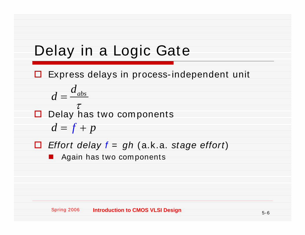
Delay in a Logic GateExpress delays in process-independent unit
Delay has two components
absd dτ
=
d f p= +
5-6Introduction to CMOS VLSI DesignSpring 2006
Delay in a Logic GateExpress delays in process-independent unit
Delay has two components
Effort delay f = gh (a.k.a. stage effort)Again has two components
absddτ
=
d pf= +

5-7Introduction to CMOS VLSI DesignSpring 2006
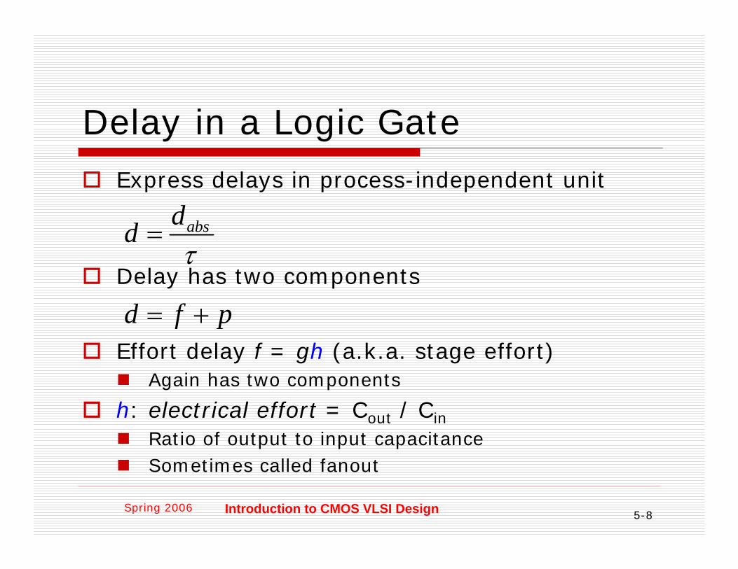
Delay in a Logic GateExpress delays in process-independent unit
Delay has two components
Effort delay f = gh (a.k.a. stage effort)Again has two components
g: logical effortMeasures relative ability of gate to deliver currentg ≡ 1 for inverter
absddτ
=
d f p= +
5-8Introduction to CMOS VLSI DesignSpring 2006
Delay in a Logic GateExpress delays in process-independent unit
Delay has two components
Effort delay f = gh (a.k.a. stage effort)Again has two components
h: electrical effort = Cout / CinRatio of output to input capacitanceSometimes called fanout
absddτ
=
d f p= +

5-9Introduction to CMOS VLSI DesignSpring 2006
Delay in a Logic GateExpress delays in process-independent unit
Delay has two components
Parasitic delay pRepresents delay of gate driving no loadSet by internal parasitic capacitance
absddτ
=
d pf= +

5-10Introduction to CMOS VLSI DesignSpring 2006
Delay Plotsd = f + p
= gh + p
Electrical Effort:h = Cout / Cin
Nor
mal
ized
Del
ay: d
Inverter2-inputNAND
g =p =d =
g =p =d =
0 1 2 3 4 5
0
1
2
3
4
5
6

5-11Introduction to CMOS VLSI DesignSpring 2006
Delay Plotsd = f + p
= gh + p
What about NOR2?
Electrical Effort:h = Cout / Cin
Nor
mal
ized
Del
ay: d
Inverter2-inputNAND
g = 1p = 1d = h + 1
g = 4/3p = 2d = (4/3)h + 2
Effort Delay: f
Parasitic Delay: p
0 1 2 3 4 5
0
1
2
3
4
5
6
5-12Introduction to CMOS VLSI DesignSpring 2006
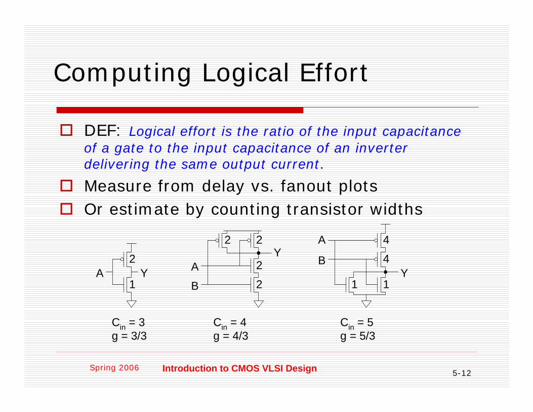
Computing Logical Effort
DEF: Logical effort is the ratio of the input capacitance of a gate to the input capacitance of an inverter delivering the same output current.
Measure from delay vs. fanout plotsOr estimate by counting transistor widths
A Y A
B
YA
BY
1
2
1 1
2 2
2
2
4
4
Cin = 3g = 3/3
Cin = 4g = 4/3
Cin = 5g = 5/3

5-13Introduction to CMOS VLSI DesignSpring 2006
Catalog of Gates
8, 16,16, 86, 12, 64, 4XOR, XNOR
22222Tristate/mux
(2n+1)/39/37/35/3NOR
(n+2)/36/35/34/3NAND
1Inverter
n4321
Number of inputsGate type
Logical effort of common gates

5-14Introduction to CMOS VLSI DesignSpring 2006
Catalog of Gates
864XOR, XNOR
2n8642Tristate / mux
n432NOR
n432NAND
1Inverter
n4321
Number of inputsGate type
Parasitic delay of common gatesIn multiples of pinv (≈1)

5-15Introduction to CMOS VLSI DesignSpring 2006
Example: Ring OscillatorEstimate the frequency of an N-stage ring oscillator
Logical Effort: g = Electrical Effort: h =Parasitic Delay: p =Stage Delay: d =Frequency: fosc =

5-16Introduction to CMOS VLSI DesignSpring 2006
Example: Ring OscillatorEstimate the frequency of an N-stage ring oscillator
Logical Effort: g = 1Electrical Effort: h = 1Parasitic Delay: p = 1Stage Delay: d = 2Frequency: fosc = 1/(2*N*d) = 1/4N
31 stage ring oscillator in 0.6 μm process has frequency of ~ 200 MHz
5-17Introduction to CMOS VLSI DesignSpring 2006
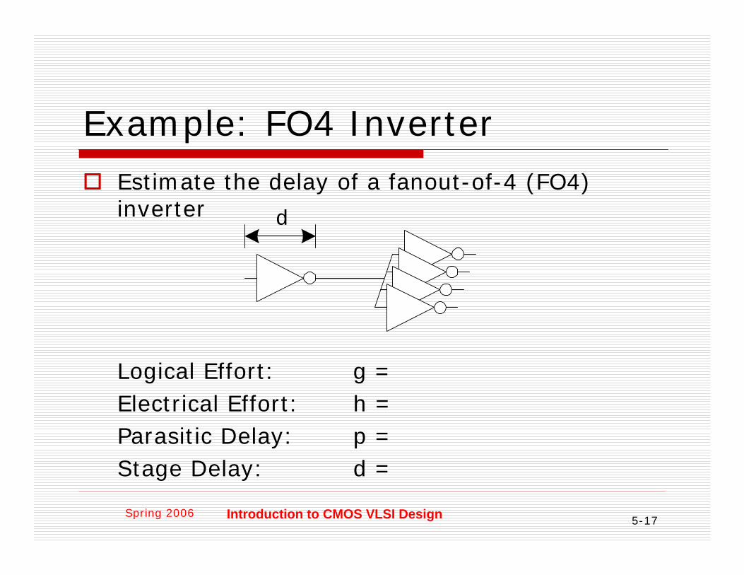
Example: FO4 InverterEstimate the delay of a fanout-of-4 (FO4) inverter
Logical Effort: g = Electrical Effort: h =Parasitic Delay: p =Stage Delay: d =
d

5-18Introduction to CMOS VLSI DesignSpring 2006
Example: FO4 InverterEstimate the delay of a fanout-of-4 (FO4) inverter
Logical Effort: g = 1Electrical Effort: h = 4Parasitic Delay: p = 1Stage Delay: d = 5
d
The FO4 delay is about
200 ps in 0.6 μm process
60 ps in a 180 nm process
f/3 ns in an f μm process

5-19Introduction to CMOS VLSI DesignSpring 2006
Multistage Logic Networks
Logical effort generalizes to multistage networksPath Logical Effort
Path Electrical Effort
Path Effort
iG g= ∏out-path
in-path
CH
C=
i i iF f g h= =∏ ∏10 x y z 20g1 = 1h1 = x/10
g2 = 5/3h2 = y/x
g3 = 4/3h3 = z/y
g4 = 1h4 = 20/z

5-20Introduction to CMOS VLSI DesignSpring 2006
Multistage Logic Networks
Logical effort generalizes to multistage networksPath Logical Effort
Path Electrical Effort
Path Effort
Can we write F = GH?
iG g= ∏out path
in path
CH
C−
−
=
i i iF f g h= =∏ ∏

5-21Introduction to CMOS VLSI DesignSpring 2006
Paths that BranchNo! Consider paths that branch:
G =H =GH =h1 =h2 =F = GH?
5
15
1590
90

5-22Introduction to CMOS VLSI DesignSpring 2006
Paths that BranchNo! Consider paths that branch:
G = 1H = 90 / 5 = 18GH = 18h1 = (15 +15) / 5 = 6h2 = 90 / 15 = 6F = g1g2h1h2 = 36 = 2GH
5
15
1590
90

5-23Introduction to CMOS VLSI DesignSpring 2006
Branching EffortIntroduce branching effort
Accounts for branching between stages in path
Now we compute the path effortF = GBH
on path off path
on path
C Cb
C+
=
iB b= ∏ih BH=∏
Note:

5-24Introduction to CMOS VLSI DesignSpring 2006
Multistage DelaysPath Effort Delay
Path Parasitic Delay
Path Delay
F iD f= ∑
iP p= ∑i FD d D P= = +∑

5-25Introduction to CMOS VLSI DesignSpring 2006
Designing Fast Circuits
Delay is smallest when each stage bears same effort
Thus minimum delay of N stage path is
This is a key result of logical effortFind fastest possible delayDoesn’t require calculating gate sizes
i FD d D P= = +∑
1ˆ Ni if g h F= =
1ND NF P= +

5-26Introduction to CMOS VLSI DesignSpring 2006
Gate SizesHow wide should the gates be for least delay?
Working backward, apply capacitance transformation to find input capacitance of each gate given load it drives.Check work by verifying input cap spec is met.
ˆ
ˆ
out
in
i
i
CC
i outin
f gh g
g CC
f
= =
⇒ =

5-27Introduction to CMOS VLSI DesignSpring 2006
Example: 3-stage pathSelect gate sizes x and y for least delay from A to B
8 x
x
x
y
y
45
45
AB

5-28Introduction to CMOS VLSI DesignSpring 2006
Example: 3-stage path
Logical Effort G = Electrical Effort H =Branching Effort B =Path Effort F =Best Stage EffortParasitic Delay P =Delay D =
8 x
x
x
y
y
45
45
AB
f̂ =

5-29Introduction to CMOS VLSI DesignSpring 2006
Example: 3-stage path
Logical Effort G = (4/3)*(5/3)*(5/3) = 100/27Electrical Effort H = 45/8Branching Effort B = 3 * 2 = 6Path Effort F = GBH = 125Best Stage EffortParasitic Delay P = 2 + 3 + 2 = 7Delay D = 3*5 + 7 = 22 = 4.4 FO4
8 x
x
x
y
y
45
45
AB
3ˆ 5f F= =

5-30Introduction to CMOS VLSI DesignSpring 2006
Example: 3-stage pathWork backward for sizesy =x =
8 x
x
x
y
y
45
45
AB

5-31Introduction to CMOS VLSI DesignSpring 2006
Example: 3-stage pathWork backward for sizesy = 45 * (5/3) / 5 = 15x = (15*2) * (5/3) / 5 = 10
P: 4N: 4
45
45
AB
P: 4N: 6 P: 12
N: 3

5-32Introduction to CMOS VLSI DesignSpring 2006
Best Number of StagesHow many stages should a path use?
Minimizing number of stages is not always fastest
Example: drive 64-bit datapath with unit inverter
D =
1 1 1 1
64 64 64 64
Initial Driver
Datapath Load
N:f:D:
1 2 3 4
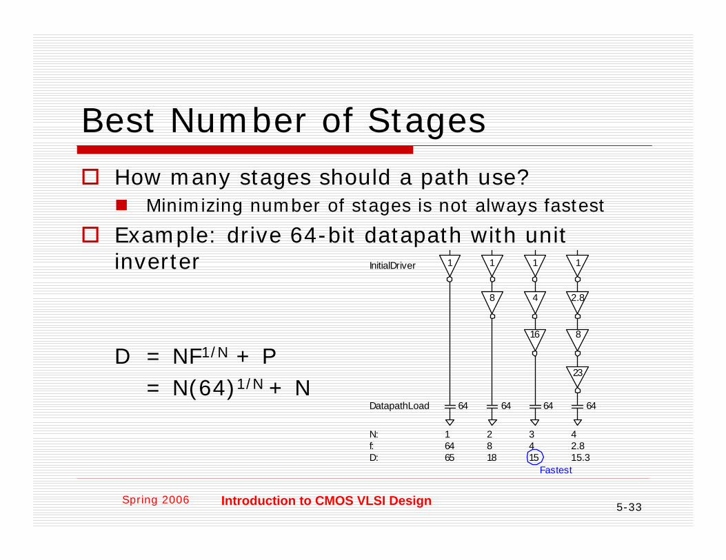
5-33Introduction to CMOS VLSI DesignSpring 2006
Best Number of StagesHow many stages should a path use?
Minimizing number of stages is not always fastest
Example: drive 64-bit datapath with unit inverter
D = NF1/N + P= N(64)1/N + N
1 1 1 1
8 4
16 8
2.8
23
64 64 64 64
Initial Driver
Datapath Load
N:f:D:
16465
2818
3415
42.815.3
Fastest
5-34Introduction to CMOS VLSI DesignSpring 2006
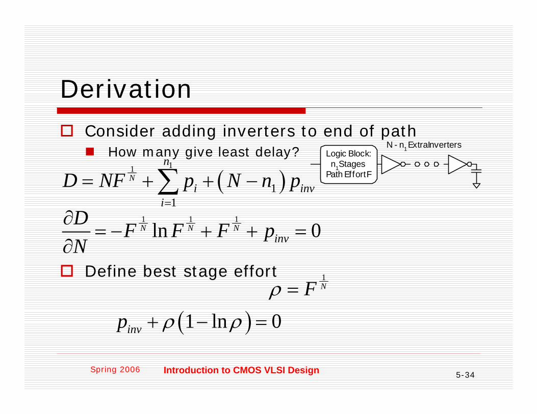
DerivationConsider adding inverters to end of path
How many give least delay?
Define best stage effort
N - n1 Extra InvertersLogic Block:n1 Stages
Path Effort F( )11
11
N
n
i invi
D NF p N n p=
= + + −∑1 1 1
ln 0N N Ninv
D F F F pN
∂= − + + =
∂
( )1 ln 0invp ρ ρ+ − =
1NFρ =

5-35Introduction to CMOS VLSI DesignSpring 2006
Best Stage Efforthas no closed-form
solution
Neglecting parasitics (pinv = 0), we find ρ = 2.718 (e)For pinv = 1, solve numerically for ρ = 3.59
( )1 ln 0invp ρ ρ+ − =

5-36Introduction to CMOS VLSI DesignSpring 2006
Sensitivity AnalysisHow sensitive is delay to using exactly the best number of stages?
2.4 < ρ < 6 gives delay within 15% of optimalUse ρ = 4
1.0
1.2
1.4
1.6
1.0 2.00.5 1.40.7
N / N
1.151.26
1.51
(ρ =2.4)(ρ=6)
D(N)
/D(N
)
0.0

5-37Introduction to CMOS VLSI DesignSpring 2006
ExampleHow do we design an address decoder? Decoder specifications:
16 word register fileEach word is 32 bits wideEach bit presents load of 3 unit-sized transistorsTrue and complementary address inputs A[3:0]Each input may drive 10 unit-sized transistors
Decisions:How many stages to use?How large should each gate be?How fast can decoder operate?
A[3:0] A[3:0]
16
32 bits
16 words
4:16 Decoder
Register File

5-38Introduction to CMOS VLSI DesignSpring 2006
Number of StagesDecoder effort is mainly electrical and branchingElectrical Effort: H =Branching Effort: B =
If we neglect logical effort (assume G = 1)Path Effort: F =
Number of Stages: N =

5-39Introduction to CMOS VLSI DesignSpring 2006
Number of StagesDecoder effort is mainly electrical and branchingElectrical Effort: H = (32*3) / 10 = 9.6Branching Effort: B = 8
If we neglect logical effort (assume G = 1)Path Effort: F = GBH = 76.8
Number of Stages: N = log4F = 3.1Try a 3-stage design

5-40Introduction to CMOS VLSI DesignSpring 2006
Gate Sizes & DelayLogical Effort: G =Path Effort: F =Stage Effort:Path Delay:Gate sizes: z = y =
A[3] A[3] A[2] A[2] A[1] A[1] A[0] A[0]
word[0]
word[15]
96 units of wordline capacitance
10 10 10 10 10 10 10 10
y z
y z
f̂ =D =

5-41Introduction to CMOS VLSI DesignSpring 2006
Gate Sizes & DelayLogical Effort: G = 1 * 6/3 * 1 = 2
Path Effort: F = GBH = 154
Stage Effort:Path Delay:Gate sizes: z = 96*1/5.36 = 18 y = 18*2/5.36 = 6.7
A[3] A[3] A[2] A[2] A[1] A[1] A[0] A[0]
word[0]
word[15]
96 units of wordline capacitance
10 10 10 10 10 10 10 10
y z
y z
1/3ˆ 5.36f F= =ˆ3 1 4 1 22.1D f= + + + =

5-42Introduction to CMOS VLSI DesignSpring 2006
ComparisonCompare many alternatives with a spreadsheet
21.6816/96NAND2-INV-NAND2-INV-INV-INV
20.4716/95INV-NAND2-INV-NAND2-INV
19.7616/94NAND2-INV-NAND2-INV
20.5620/94NAND2-NOR2-INV-INV
21.1724NAND4-INV-INV-INV
22.1623INV-NAND4-INV
30.1420/92NAND2-NOR2
29.8522NAND4-INV
DPGNDesign

5-43Introduction to CMOS VLSI DesignSpring 2006
Review of Definitions
delay
parasitic delay
effort delay
effort
branching effort
electrical effort
logical effort
number of stages
PathStageTerm
iG g= ∏out-path
in-path
CCH =
N
iB b= ∏F GBH=
F iD f= ∑
iP p= ∑i FD d D P= = +∑
out
in
CCh =
on-path off-path
on-path
C CCb +=
f gh=
f
p
d f p= +
g
1
5-44Introduction to CMOS VLSI DesignSpring 2006
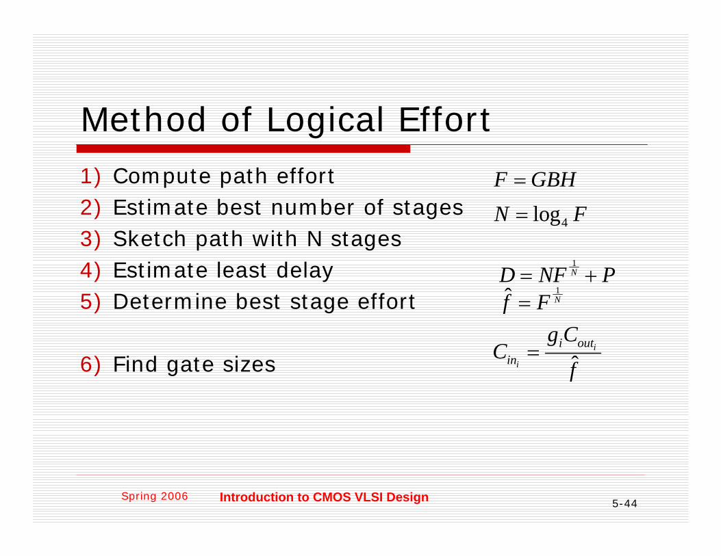
Method of Logical Effort1) Compute path effort2) Estimate best number of stages3) Sketch path with N stages4) Estimate least delay5) Determine best stage effort
6) Find gate sizes
F GBH=
4logN F=
1ND NF P= +
1ˆ Nf F=
ˆi
i
i outin
g CC
f=

5-45Introduction to CMOS VLSI DesignSpring 2006
Limits of Logical EffortChicken and egg problem
Need path to compute GBut don’t know number of stages without G
Simplistic delay modelNeglects input rise time effects
InterconnectIteration required in designs with wire
Maximum speed onlyNot minimum area/power for constrained delay

5-46Introduction to CMOS VLSI DesignSpring 2006
SummaryLogical effort is useful for thinking of delay in circuits
Numeric logical effort characterizes gatesNANDs are faster than NORs in CMOSPaths are fastest when effort delays are ~4Path delay is weakly sensitive to stages, sizesBut using fewer stages doesn’t mean faster pathsDelay of path is about log4F FO4 inverter delaysInverters and NAND2 best for driving large caps
Provides language for discussing fast circuitsBut requires practice to master