
Redefining the Foundry Model Panel Discussion at ITAC - GSANorm ArmourVice President and General Manager, Fab 8

Overview
The endless march of technologyIncreasing complexity and cost in manufacturing
An industry in transitionThe shift from regional to global
Creating a sustainable modelCollaboration essential to innovation
The next evolution in the industryFrom contract manufacturing to collaborative manufacturing
April 29, 2010 2GLOBALFOUNDRIES CONFIDENTIAL

2009 Market Volume (No. of end-consumer devices)
130nm180nm+ 90nm 65nm 45nm 32nmProcess linewidth Media Phone
1B
500M
250M
100M
SmartPhone
Voice Only Phone
Personal & portable stereos
MP3 Players
Video game –Handheld & console
Digital Still Cameras
Discrete GPU
IGP Chipset
MPUSet-Top Boxes
Source: Bridge & GLOBALFOUNDRIES analysis, iSuppli Mobile Handset Tracker; iSuppli Consumer Platforms Market Tracker , Mercury Reports GPU, Gartner Reports GPU
April 29, 2010 3GLOBALFOUNDRIES CONFIDENTIAL
CPUs and GPUs still drive transitions, but wireless devices are not far behind
Leading-Edge Technology Adoption
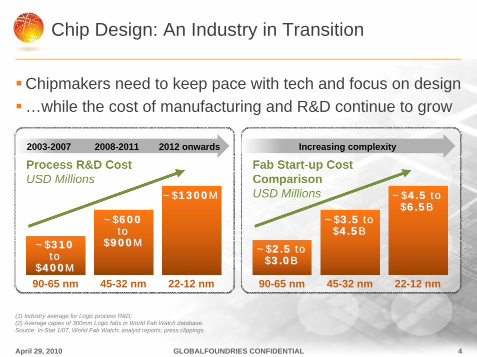
Chip Design: An Industry in Transition
Chipmakers need to keep pace with tech and focus on design…while the cost of manufacturing and R&D continue to grow
(1) Industry average for Logic process R&D; (2) Average capex of 300mm Logic fabs in World Fab Watch database. Source: In-Stat 1/07, World Fab Watch; analyst reports; press clippings.
April 29, 2010 4GLOBALFOUNDRIES CONFIDENTIAL
2003-2007 2008-2011 2012 onwards
Process R&D CostUSD Millions
90-65 nm 45-32 nm 22-12 nm
~$~$310310toto
$$400400MM
~$~$600600toto
$$900900MM
~$~$13001300MM
Increasing complexity
Fab Start-up CostComparisonUSD Millions
90-65 nm 45-32 nm 22-12 nm
~$~$2.5 2.5 toto$$3.03.0BB
~$~$3.5 3.5 toto$$4.54.5BB
~$~$4.5 4.5 toto$$6.56.5BB

The First Truly Global Foundry
East Fishkill, NY
Austin, TX
HeadquartersSi Valley, CA
London, UK
Yokohama,Japan
Shanghai,China
Hsinchu,Taiwan
Munich, Germany
Global Manufacturing and Support Footprint
Manufacturing CentersSaratoga, New York Dresden, Germany SingaporeSales and Support Offices
Dresden, Germany
Singapore
Saratoga, NY

The New GLOBALFOUNDRIES
Headquartered in Silicon ValleyApproximately 10,000 employeesSpanning three continents across 12 locations300mm Fabs in Singapore, Germany, New York200mm Fabs in Singapore
One of the World’s Largest Foundries2009 revenue of ~$2.5B US 150 Customers including many of the world’s largest IC companies
The New Leader in Foundry Technology and Service
Substantial Time-to-volume advantage for advanced technologiesDriving the Global Standard for new technologiesFull foundry offering from mainstream to leading edge with Value-Added SolutionsCommitted to Best-in-Class customer service
Germany
Singapore
New York

State-of-the-Art 300mm Fabs
Global foundry capacity expansion minimizes geographic risk
Fab 1 in Germany Fab 7 in Singapore Fab 8 in New York
• 45nm and below • 130nm to 40nm • 28nm and below
• 300mm wafers• 60,000 wafers/month
• 300mm wafers• 50,000 wafers/month
• 300mm wafers• 42,000 wafers/month
• Production Now • Production Now •Groundbreaking July 2009• Production ramping 2012
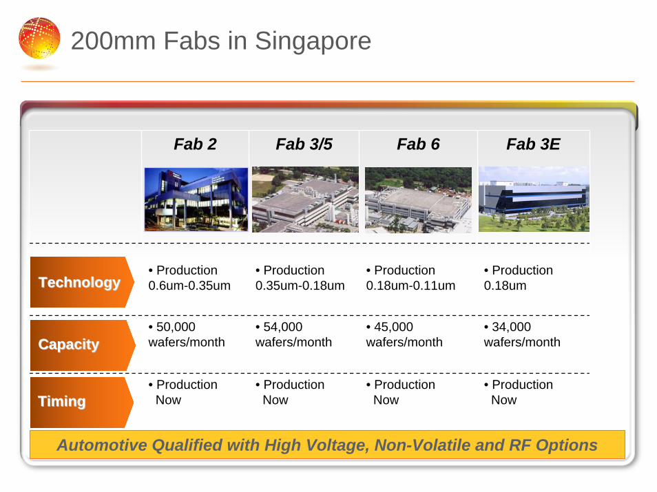
200mm Fabs in Singapore
Fab 2 Fab 3/5 Fab 6 Fab 3E
• Production 0.6um-0.35um
• Production 0.35um-0.18um
• Production 0.18um-0.11um
• Production 0.18um
• 50,000 wafers/month
• 54,000 wafers/month
• 45,000 wafers/month
• 34,000 wafers/month
• Production Now
• Production Now
• Production Now
• Production Now
TechnologyTechnology
CapacityCapacity
Timing Timing
Automotive Qualified with High Voltage, Non-Volatile and RF Options

Shared objectivesEarly-stage leading-edge R&DProduction-ready process technologies
Shared investmentsAdvanced manufacturing resourcesDiverse teams collaborating
Face-to-face and virtual
Shared returnsAccelerated access to advanced technologiesExperience from early, high-volume production to refine processes
Rich partner/IP eco-system to support leading-edge adoption
A Model for Shared Innovation
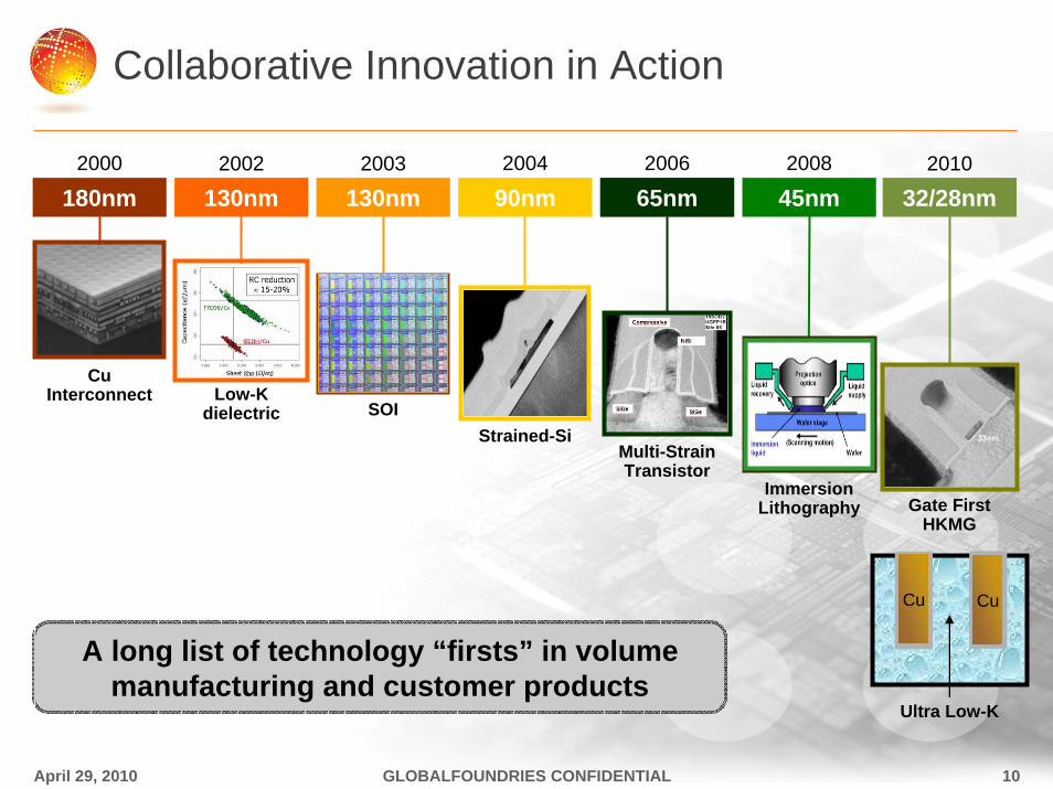
130nm2003
SOI
45nm2008
ImmersionLithography
180nm2000
CuInterconnect
90nm2004
Strained-Si
130nm2002
Low-Kdielectric
65nm2006
Multi-StrainTransistor
65nm 32/28nm
Gate First HKMG
2010
CuCu
Ultra Low-K
Collaborative Innovation in Action
April 29, 2010 10GLOBALFOUNDRIES CONFIDENTIAL
A long list of technology “firsts” in volumemanufacturing and customer products
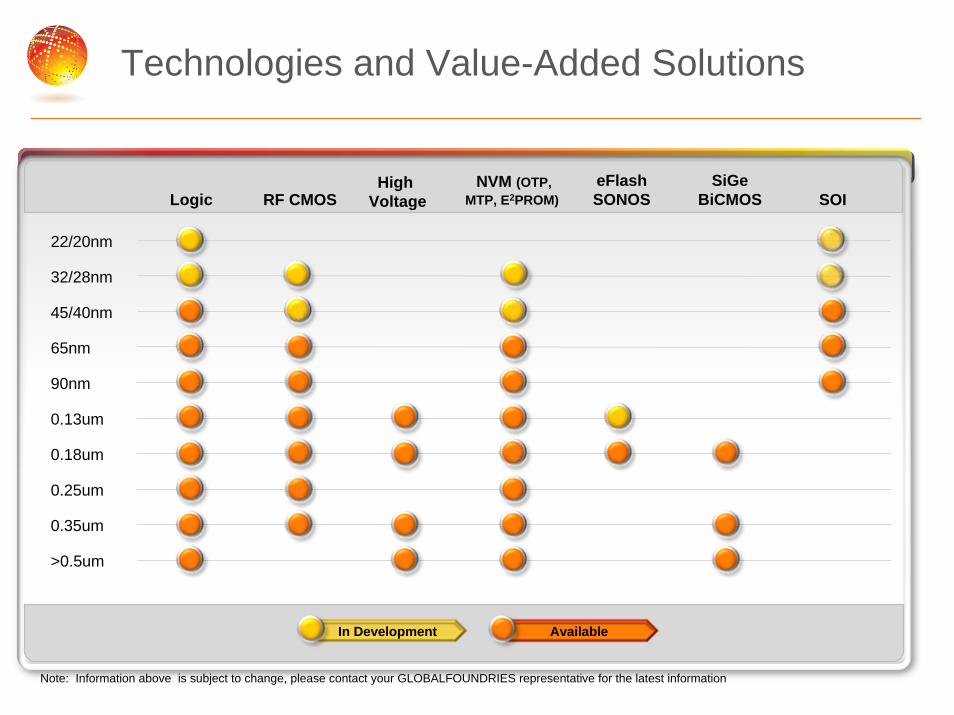
Technologies and Value-Added Solutions
Note: Information above is subject to change, please contact your GLOBALFOUNDRIES representative for the latest information
RF CMOSNVM (OTP,
MTP, E2PROM)eFlashSONOS SOI
22/20nm
32/28nm
45/40nm
65nm
90nm
0.13um
0.18um
0.25um
0.35um
>0.5um
SiGeBiCMOSLogic
High Voltage
In Development Available

Enabling Time-to-Market Leadership
As complexity of chip design increases, manufacturing partnerships become ever more critical
Closely collaborative foundry relationships are essential to enabling smooth and rapid time to market
GLOBALFOUNDRIES’ time-to-volume is unmatched in the foundry industry
– 45nm ramp far ahead of rest of foundry industry
– High-volume, complex x86 CPU drives yield learning for other customers
– Initial 32nm HKMG production running now in Fab 1
GLOBALFOUNDRIES CONFIDENTIALApril 29, 2010
45/40nm Production Ramp300mm Wafers Shipped per Quarter (1000’s)
40nm - Other Leading
Foundries*
45nm
12
*Market data compiled by International Business Strategies
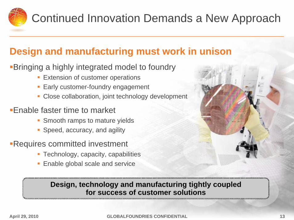
Continued Innovation Demands a New Approach
Design and manufacturing must work in unisonBringing a highly integrated model to foundry
Extension of customer operationsEarly customer-foundry engagementClose collaboration, joint technology development
Enable faster time to marketSmooth ramps to mature yieldsSpeed, accuracy, and agility
Requires committed investmentTechnology, capacity, capabilitiesEnable global scale and service
Design, technology and manufacturing tightly coupled for success of customer solutions
April 29, 2010 13GLOBALFOUNDRIES CONFIDENTIAL

Fab 8, Moduel 1

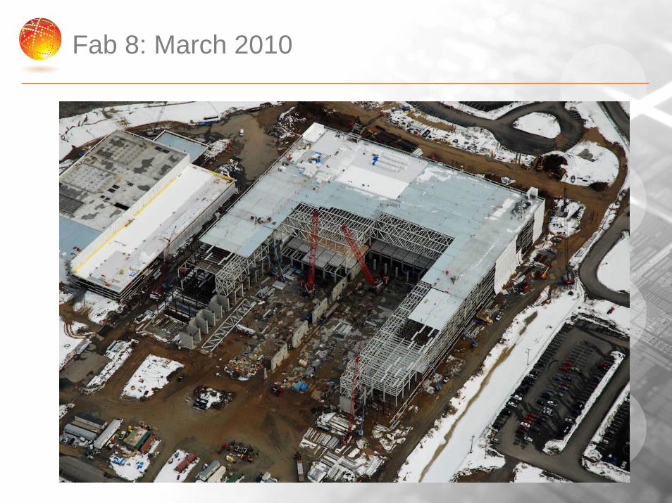
Fab 8: March 2010
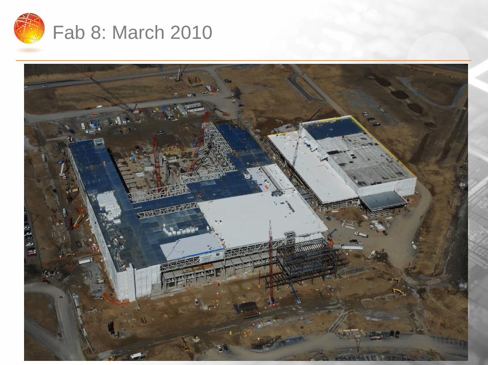
Fab 8: March 2010

Fab8 m1 (Ph1)(210k sqft)
Fab8 m1(Ph2)(90k sqft)
Campus222.45 acres
Fab8
mod
ule2
Fab8 module3
Module 1 currently under construction. There is room on the campus to build Modules 2 & 3, but thosephases are not yet planned.
Fab 8: possible campus build out design

Thank You!
GLOBALFOUNDRIES, the GLOBALFOUNDRIES logo and combinations thereof are trademarks of GLOBALFOUNDRIES Inc. in the United States and/or other jurisdictions. Other names used in this presentation are for identification purposes only and may be trademarks of their respective owners.
©2010 GLOBALFOUNDRIES Inc. All rights reserved.
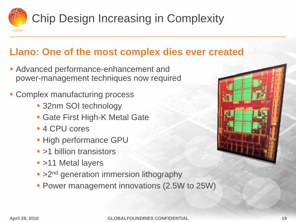
Chip Design Increasing in Complexity
Llano: One of the most complex dies ever createdAdvanced performance-enhancement and power-management techniques now required
Complex manufacturing process32nm SOI technologyGate First High-K Metal Gate4 CPU coresHigh performance GPU >1 billion transistors>11 Metal layers>2nd generation immersion lithographyPower management innovations (2.5W to 25W)
April 29, 2010 19GLOBALFOUNDRIES CONFIDENTIAL
Continuous Innovation Required
Innovation in thinkingPerformance-per-watt, battery life, parallel computing, virtualization, visual computing, small form factor
Innovation in designMultiple cores, CPU/GPU integration, embedded memory, power management, system-level architecture
Innovation in manufacturing and technologyNew materials, transistor structures, 3D stacking, immersion/EUV lithography, ultra-low k dielectrics, High-k Metal Gate
April 29, 2010 20GLOBALFOUNDRIES CONFIDENTIAL
Despite technical challenges, biggest hurdle to continued innovation is economics
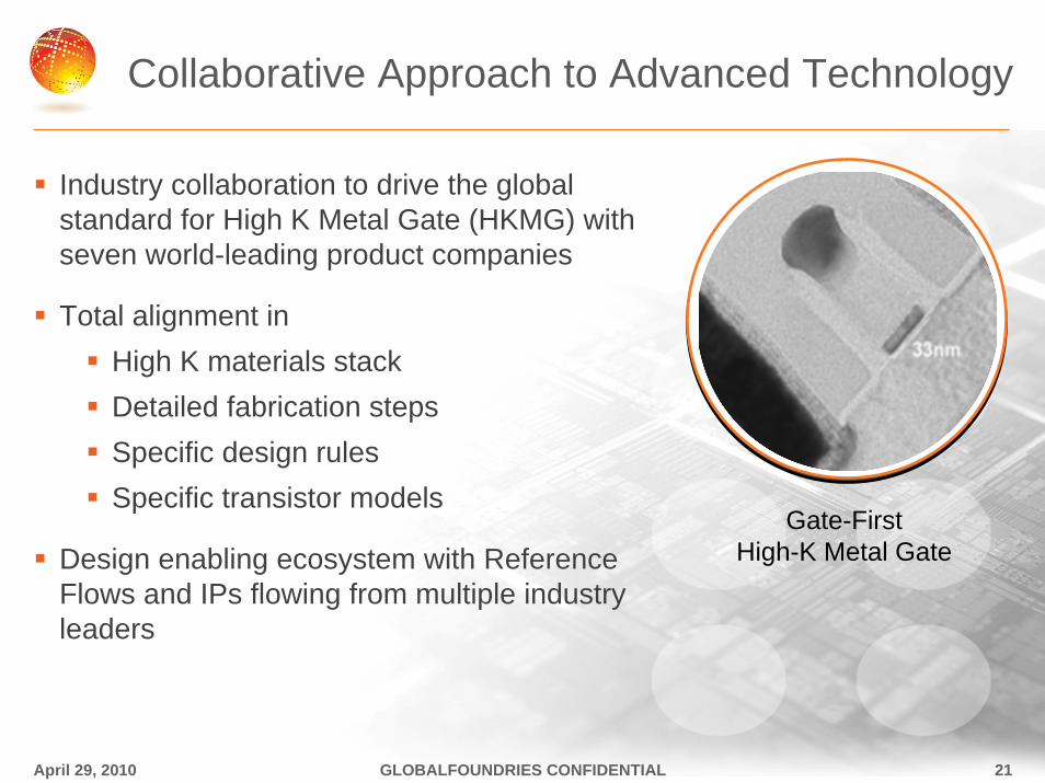
Collaborative Approach to Advanced Technology
Industry collaboration to drive the global standard for High K Metal Gate (HKMG) with seven world-leading product companies
Total alignment in High K materials stackDetailed fabrication steps Specific design rulesSpecific transistor models
Design enabling ecosystem with Reference Flows and IPs flowing from multiple industry leaders
Gate-First High-K Metal Gate
April 29, 2010 21GLOBALFOUNDRIES CONFIDENTIAL
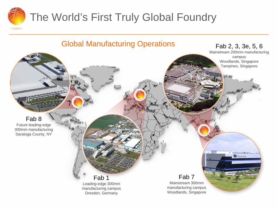
The World’s First Truly Global Foundry
Fab 8Future leading-edge
300mm manufacturingSaratoga County, NY
Fab 1Leading-edge 300mm manufacturing campus
Dresden, Germany
Fab 2, 3, 3e, 5, 6Mainstream 200mm manufacturing
campusWoodlands, SingaporeTampines, Singapore
Fab 7Mainstream 300mm
manufacturing campusWoodlands, Singapore
Global Manufacturing Operations

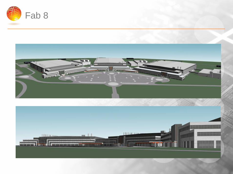
Fab 8
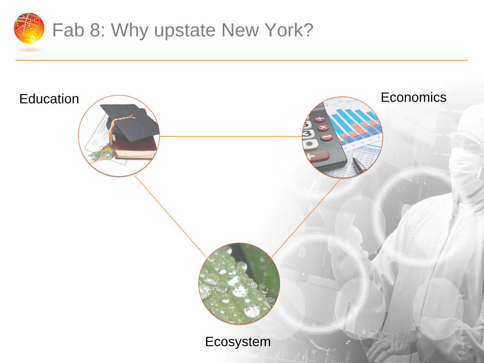
Fab 8: Why upstate New York?
Education Economics
Ecosystem
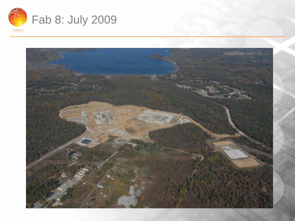
Fab 8: July 2009

Fab 8: December 2009
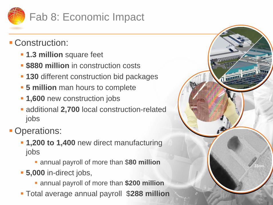
Fab 8: Economic Impact
Construction:1.3 million square feet$880 million in construction costs130 different construction bid packages5 million man hours to complete1,600 new construction jobsadditional 2,700 local construction-related jobs
Operations:1,200 to 1,400 new direct manufacturing jobs
annual payroll of more than $80 million 5,000 in-direct jobs,
annual payroll of more than $200 millionTotal average annual payroll $288 million

Fab 8: concrete foundation

Fab 8: vertical concrete walls
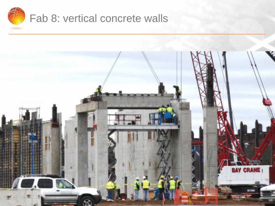
Fab 8: vertical concrete walls
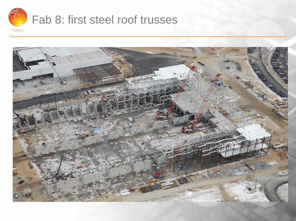
Fab 8: first steel roof trusses
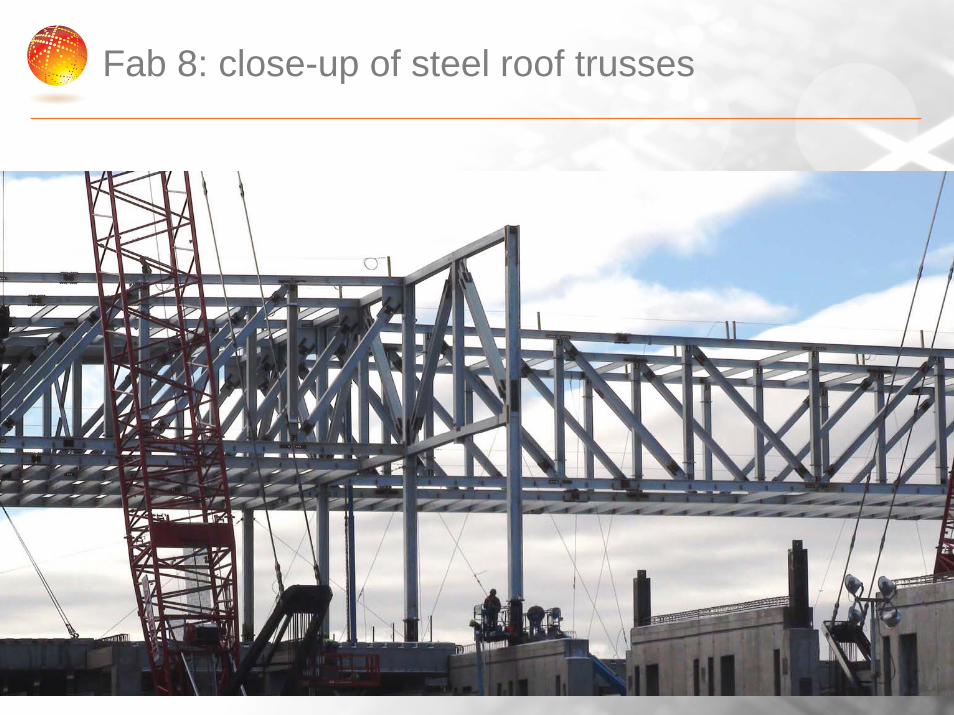
Fab 8: close-up of steel roof trusses
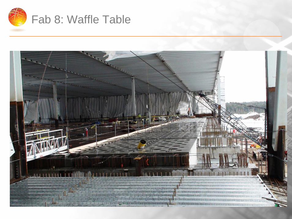
Fab 8: Waffle Table
Fab 8: March 2010
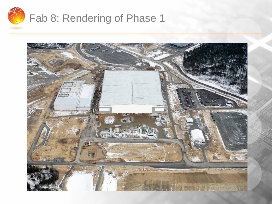
Fab 8: Rendering of Phase 1

Fab 8: potential Phase2 expansion completion - 300k ft-2 (27.9k m-2)
Phase1Phase2

Fab 8: February 2010
Fab 8


