1
Digital Electronics
Part II – Electronics, Devices
and Circuits Dr. I. J. Wassell
Introduction
• In the coming lectures we will consider how
logic gates can be built using electronic
circuits
• First, basic concepts concerning electrical
circuits and components will be introduced
• This will enable the analysis of linear circuits,
i.e., one where superposition applies:
– If an input x1(t) gives an output y1(t), and input
x2(t) gives an output y2(t), then input [x1(t)+x2(t)]
gives an output [y1(t)+y2(t)]
2
Introduction
• However, logic circuits are non-linear,
consequently we will introduce a graphical
technique for analysing such circuits
• Semiconductor materials, junction diodes and
field effect transistors (FET) will be introduced
• The construction of an NMOS inverter from an
n-channel (FET) will then be described
• Finally, CMOS logic built using FETs will then
be presented
Basic Electricity
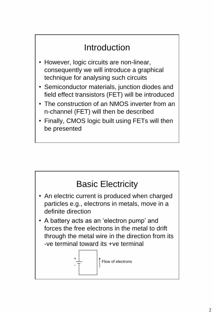
• An electric current is produced when charged
particles e.g., electrons in metals, move in a
definite direction
• A battery acts as an ‘electron pump’ and
forces the free electrons in the metal to drift
through the metal wire in the direction from its
-ve terminal toward its +ve terminal
+
- Flow of electrons
3
Basic Electricity
• Actually, before electrons were discovered it
was imagined that the flow of current was due
to positively charged particles flowing out of
+ve toward –ve battery terminal
• Indeed, the positive direction of current flow is
still defined in this way!
• The unit of charge is the Coulomb (C). One
Coulomb is equivalent to the charge carried
by 6.25*1018 electrons (since one electron has
a charge of 1.6*10-19 Coulombs).
Basic Electricity
• Current is defined as the rate of flow of
charge, i.e., a flow of 1 Coulomb (C) in 1
second is defined as 1 Ampere (A).
• In the circuit shown in the earlier slide, it is the
battery that supplies the electrical force and
energy that drives the electrons round the
circuit.
• In doing so, the electrons give up most of their
energy as heat as the temperature of the
metal wire rises.
4
Basic Electricity
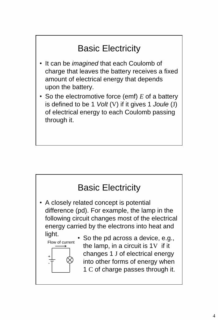
• It can be imagined that each Coulomb of
charge that leaves the battery receives a fixed
amount of electrical energy that depends
upon the battery.
• So the electromotive force (emf) E of a battery
is defined to be 1 Volt (V) if it gives 1 Joule (J)
of electrical energy to each Coulomb passing
through it.
Basic Electricity
• A closely related concept is potential
difference (pd). For example, the lamp in the
following circuit changes most of the electrical
energy carried by the electrons into heat and
light.
+
-
Flow of current • So the pd across a device, e.g.,
the lamp, in a circuit is 1V if it
changes 1 J of electrical energy
into other forms of energy when
1 C of charge passes through it.
5
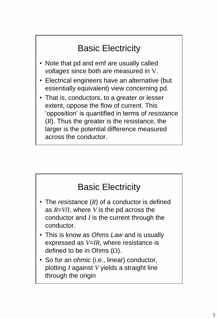
Basic Electricity
• Note that pd and emf are usually called
voltages since both are measured in V.
• Electrical engineers have an alternative (but
essentially equivalent) view concerning pd.
• That is, conductors, to a greater or lesser
extent, oppose the flow of current. This
‘opposition’ is quantified in terms of resistance
(R). Thus the greater is the resistance, the
larger is the potential difference measured
across the conductor.
Basic Electricity
• The resistance (R) of a conductor is defined
as R=V/I, where V is the pd across the
conductor and I is the current through the
conductor.
• This is know as Ohms Law and is usually
expressed as V=IR, where resistance is
defined to be in Ohms (W).
• So for an ohmic (i.e., linear) conductor,
plotting I against V yields a straight line
through the origin
6
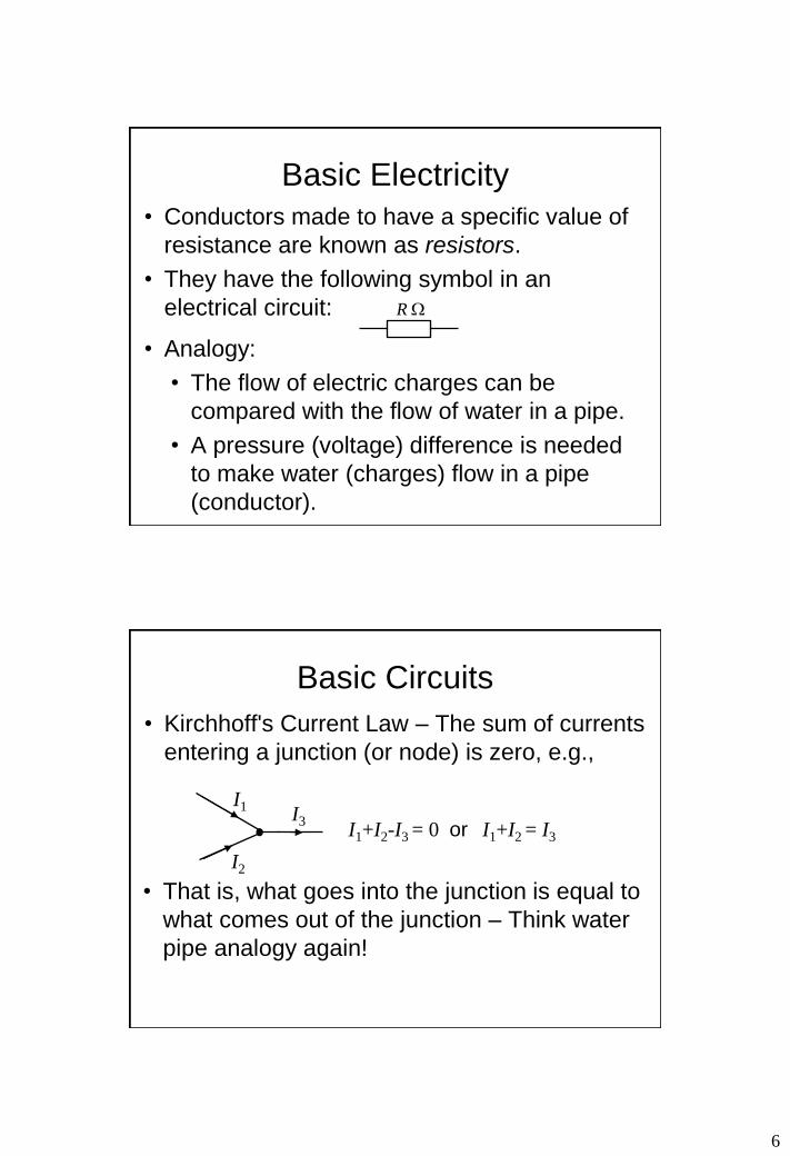
Basic Electricity
• Conductors made to have a specific value of
resistance are known as resistors.
• They have the following symbol in an
electrical circuit: R W
• Analogy:
• The flow of electric charges can be
compared with the flow of water in a pipe.
• A pressure (voltage) difference is needed
to make water (charges) flow in a pipe
(conductor).
Basic Circuits
• Kirchhoff's Current Law – The sum of currents
entering a junction (or node) is zero, e.g.,
I1
I2
I3 I1+I2-I3 = 0 or I1+I2 = I3
• That is, what goes into the junction is equal to
what comes out of the junction – Think water
pipe analogy again!
7
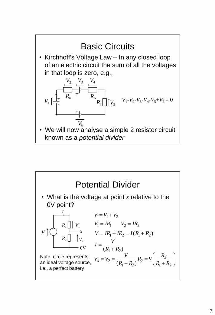
Basic Circuits • Kirchhoff's Voltage Law – In any closed loop
of an electric circuit the sum of all the voltages
in that loop is zero, e.g.,
V1-V2-V3-V4-V5+V6 = 0 V5
+ -
+
+
Ra Rb
Rc V1
V2 V3 V4
V6
• We will now analyse a simple 2 resistor circuit
known as a potential divider
Potential Divider
V
R1
R2
I
x
V1
V2
0V
• What is the voltage at point x relative to the
0V point?
21 VVV
11 IRV 22 IRV
)( 2121 RRIIRIRV
)( 21 RR
VI
21
22
212
)( RR
RVR
RR
VVVx
Note: circle represents
an ideal voltage source,
i.e., a perfect battery

8
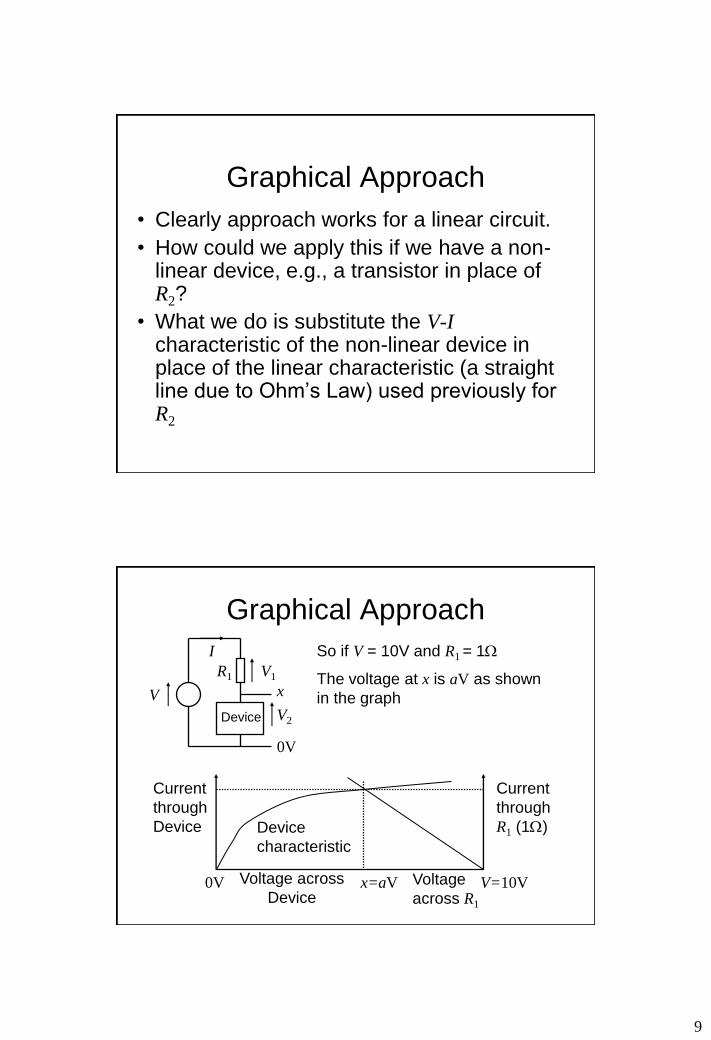
Solving Non-linear circuits
• As mentioned previously, not all electronic devices have linear I-V characteristics, importantly in our case this includes the FETs used to build logic circuits
• Consequently we cannot easily use the algebraic approach applied previously to the potential divider. Instead, we will use a graphical approach
• Firstly though, we will apply the graphical approach to the potential divider example
Potential Divider • How can we do this graphically?
V
R1
R2
I
x
V1
V2
0V
So if V = 10V, R1 = 1W and R2 = 2W
V7.621
210
21
2
RR
RVVx
Current
through
R2 (2W)
Current
through
R1 (1W)
x=6.7V V=10V 0V Voltage
across R2
Voltage
across R1
9
Graphical Approach
• Clearly approach works for a linear circuit.
• How could we apply this if we have a non-linear device, e.g., a transistor in place of R2?
• What we do is substitute the V-I characteristic of the non-linear device in place of the linear characteristic (a straight line due to Ohm’s Law) used previously for R2
Graphical Approach
V
R1
Device
I
x
V1
V2
0V
Current
through
Device
Current
through
R1 (1W)
x=aV V=10V 0V Voltage across
Device Voltage
across R1
So if V = 10V and R1 = 1W
Device
characteristic
The voltage at x is aV as shown
in the graph
10
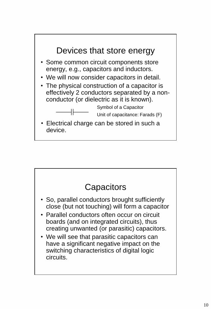
Devices that store energy
• Some common circuit components store energy, e.g., capacitors and inductors.
• We will now consider capacitors in detail.
• The physical construction of a capacitor is effectively 2 conductors separated by a non-conductor (or dielectric as it is known).
• Electrical charge can be stored in such a device.
Symbol of a Capacitor
Unit of capacitance: Farads (F)
Capacitors
• So, parallel conductors brought sufficiently close (but not touching) will form a capacitor
• Parallel conductors often occur on circuit boards (and on integrated circuits), thus creating unwanted (or parasitic) capacitors.
• We will see that parasitic capacitors can have a significant negative impact on the switching characteristics of digital logic circuits.
11
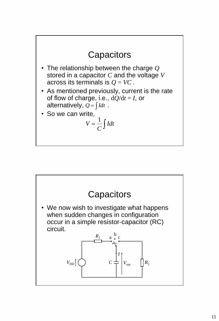
Capacitors
• The relationship between the charge Q stored in a capacitor C and the voltage V across its terminals is Q = VC .
• As mentioned previously, current is the rate of flow of charge, i.e., dQ/dt = I, or alternatively, .
• So we can write, IdtQ
IdtC
V1
Capacitors
• We now wish to investigate what happens when sudden changes in configuration occur in a simple resistor-capacitor (RC) circuit.
VDD
R1
Vout C
I
R2
a c b
12
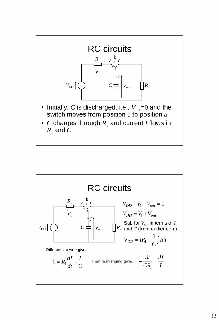
RC circuits
• Initially, C is discharged, i.e., Vout=0 and the switch moves from position b to position a
• C charges through R1 and current I flows in R1 and C
R2 VDD
R1
Vout C
I
a c b
V1
RC circuits b
R2 VDD
R1
Vout C
I
a c
V1
01 outDD VVV
outDD VVV 1
IdtC
IRVDD
11
Sub for Vout in terms of I
and C (from earlier eqn.)
I
dI
CR
dt
1C
I
dt
dIR 10
Differentiate wrt t gives
Then rearranging gives
13
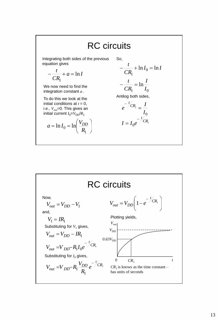
RC circuits
Integrating both sides of the previous
equation gives
IaCR
tln
1
10 lnln
R
VIa DD
So,
We now need to find the
integration constant a .
To do this we look at the
initial conditions at t = 0,
i.e., Vout=0. This gives an
initial current I0=VDD/R1
01
01
ln
lnln
I
I
CR
t
IICR
t
Antilog both sides,
0
1
I
Ie
CRt
1
0CR
t
eII
RC circuits
Now,
1VVV DDout
Plotting yields,
1
01
1
CRt
DDout
DDout
eIRVV
IRVV
and,
11 IRV
Substituting for V1 gives,
1
11
CRt
DDDDout e
R
VRVV
Substituting for I0 gives,
11
CRt
DDout eVV
Vout
t 0
VDD
0.63VDD
CR1
CR1 is knows as the time constant –
has units of seconds

14
RC circuits
• Initially assume C is fully charged, i.e., Vout=VDD and the switch moves from position a to position c
• C discharges through R2 and current flows in R2 and C
R2 VDD
R1
Vout C
I
a c b
V1
RC circuits
The expression for Vout is,
2CRt
DDout eVV
Plotting yields, Vout
t 0
VDD
0.37VDD
CR2
R2 VDD
R1
Vout C
I
a c b
V1
15
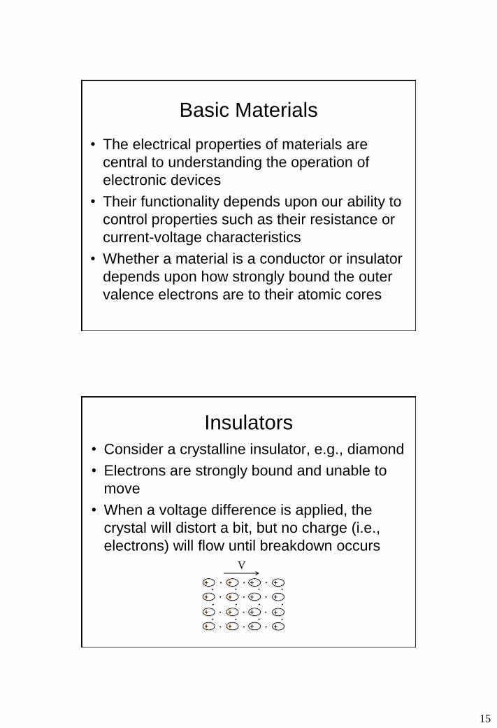
Basic Materials
• The electrical properties of materials are
central to understanding the operation of
electronic devices
• Their functionality depends upon our ability to
control properties such as their resistance or
current-voltage characteristics
• Whether a material is a conductor or insulator
depends upon how strongly bound the outer
valence electrons are to their atomic cores
Insulators
• Consider a crystalline insulator, e.g., diamond
• Electrons are strongly bound and unable to
move
• When a voltage difference is applied, the
crystal will distort a bit, but no charge (i.e.,
electrons) will flow until breakdown occurs
V
16
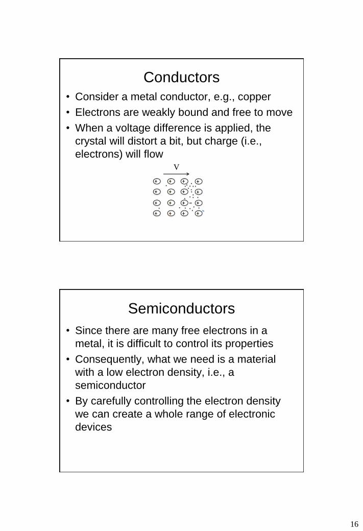
Conductors
• Consider a metal conductor, e.g., copper
• Electrons are weakly bound and free to move
• When a voltage difference is applied, the
crystal will distort a bit, but charge (i.e.,
electrons) will flow V
Semiconductors
• Since there are many free electrons in a
metal, it is difficult to control its properties
• Consequently, what we need is a material
with a low electron density, i.e., a
semiconductor
• By carefully controlling the electron density
we can create a whole range of electronic
devices
17
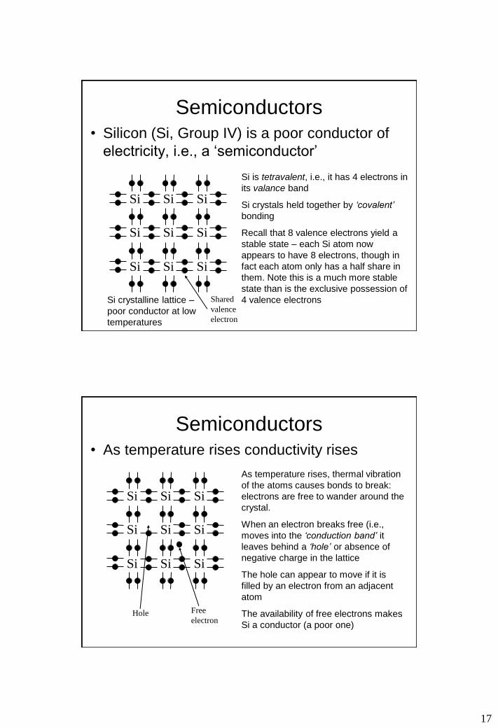
Semiconductors
Si crystalline lattice –
poor conductor at low
temperatures
Si is tetravalent, i.e., it has 4 electrons in
its valance band
Si crystals held together by ‘covalent’
bonding
Recall that 8 valence electrons yield a
stable state – each Si atom now
appears to have 8 electrons, though in
fact each atom only has a half share in
them. Note this is a much more stable
state than is the exclusive possession of
4 valence electrons
• Silicon (Si, Group IV) is a poor conductor of
electricity, i.e., a ‘semiconductor’
Si
Si
Si
Si
Si
Si
Si
Si
Si
Shared
valence
electron
Semiconductors
As temperature rises, thermal vibration
of the atoms causes bonds to break:
electrons are free to wander around the
crystal.
When an electron breaks free (i.e.,
moves into the ‘conduction band’ it
leaves behind a ‘hole’ or absence of
negative charge in the lattice
The hole can appear to move if it is
filled by an electron from an adjacent
atom
The availability of free electrons makes
Si a conductor (a poor one)
• As temperature rises conductivity rises
Si
Si
Si
Si
Si
Si
Si
Si
Si
Free
electron Hole
18
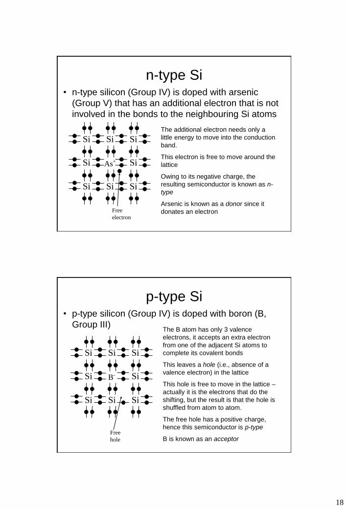
n-type Si
The additional electron needs only a
little energy to move into the conduction
band.
This electron is free to move around the
lattice
Owing to its negative charge, the
resulting semiconductor is known as n-
type
Arsenic is known as a donor since it
donates an electron
• n-type silicon (Group IV) is doped with arsenic
(Group V) that has an additional electron that is not
involved in the bonds to the neighbouring Si atoms
Free
electron
Si
Si
Si
Si
As+
Si
Si
Si
Si
p-type Si
The B atom has only 3 valence
electrons, it accepts an extra electron
from one of the adjacent Si atoms to
complete its covalent bonds
This leaves a hole (i.e., absence of a
valence electron) in the lattice
This hole is free to move in the lattice –
actually it is the electrons that do the
shifting, but the result is that the hole is
shuffled from atom to atom.
The free hole has a positive charge,
hence this semiconductor is p-type
B is known as an acceptor
• p-type silicon (Group IV) is doped with boron (B,
Group III)
Free
hole
Si
Si
Si
Si
B-
Si
Si
Si
Si
19
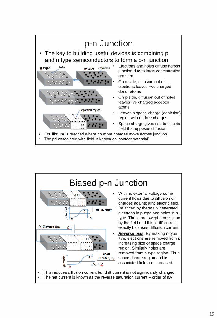
p-n Junction • The key to building useful devices is combining p
and n type semiconductors to form a p-n junction • Electrons and holes diffuse across
junction due to large concentration
gradient
• On n-side, diffusion out of
electrons leaves +ve charged
donor atoms
• On p-side, diffusion out of holes
leaves -ve charged acceptor
atoms
• Leaves a space-charge (depletion)
region with no free charges
• Space charge gives rise to electric
field that opposes diffusion
• Equilibrium is reached where no more charges move across junction
• The pd associated with field is known as ‘contact potential’
Biased p-n Junction • With no external voltage some
current flows due to diffusion of
charges against junc electric field.
Balanced by thermally generated
electrons in p-type and holes in n-
type. These are swept across junc
by the field and this ‘drift’ current
exactly balances diffusion current
• Reverse bias: By making n-type
+ve, electrons are removed from it
increasing size of space charge
region. Similarly holes are
removed from p-type region. Thus
space charge region and its
associated field are increased.
• This reduces diffusion current but drift current is not significantly changed
• The net current is known as the reverse saturation current – order of nA
20
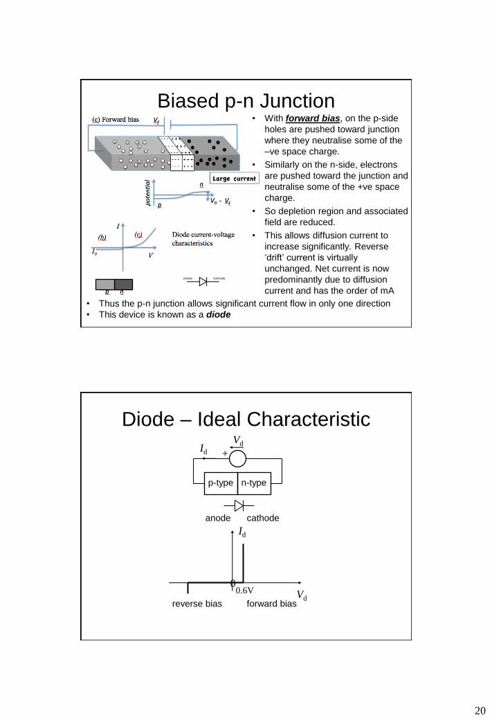
Biased p-n Junction
• Thus the p-n junction allows significant current flow in only one direction
• This device is known as a diode
• With forward bias, on the p-side
holes are pushed toward junction
where they neutralise some of the
–ve space charge.
• Similarly on the n-side, electrons
are pushed toward the junction and
neutralise some of the +ve space
charge.
• So depletion region and associated
field are reduced.
• This allows diffusion current to
increase significantly. Reverse
‘drift’ current is virtually
unchanged. Net current is now
predominantly due to diffusion
current and has the order of mA
Diode – Ideal Characteristic
p-type n-type
anode cathode
+
Vd Id
Id
Vd
0 0.6V
forward bias reverse bias

21
n-Channel MOSFET • We will now introduce a more complex
semiconductor device known as an n-channel
Metal Oxide Semiconductor Field Effect
Transistor (MOSFET) and see how it can be
used to build logic circuits
Gate
(G)
Drain
(D)
Source
(S)
The current flow from D to S
(IDS) is controlled by the voltage
applied between G and S (VGS)
We will be describing
enhancement mode devices in
which no current flows (IDS=0,
i.e., the transistor is Off) when
VGS=0V
n-Channel MOSFET
Drain (and Source) diode
reverse biased, so no path for
current to flow from S to D, i.e.,
the transistor is off
n+
n+ S
0V
G
D
+VD
p-type
Reverse
biased
p-n
junctions
Silicon
dioxide
insulator
OFF
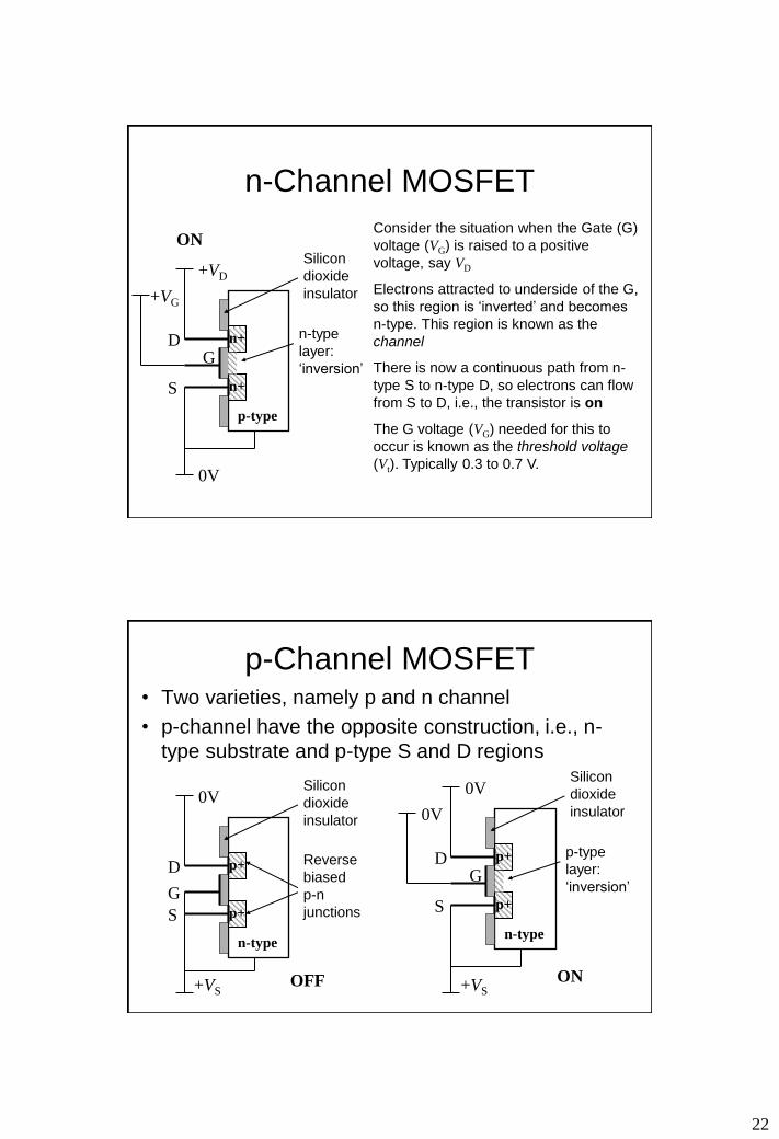
22
n-Channel MOSFET
Consider the situation when the Gate (G)
voltage (VG) is raised to a positive
voltage, say VD
Electrons attracted to underside of the G,
so this region is ‘inverted’ and becomes
n-type. This region is known as the
channel
There is now a continuous path from n-
type S to n-type D, so electrons can flow
from S to D, i.e., the transistor is on
The G voltage (VG) needed for this to
occur is known as the threshold voltage
(Vt). Typically 0.3 to 0.7 V.
n+
n+ S
0V
G D
+VD
p-type
n-type
layer:
‘inversion’
Silicon
dioxide
insulator
ON
+VG
p-Channel MOSFET • Two varieties, namely p and n channel
• p-channel have the opposite construction, i.e., n-
type substrate and p-type S and D regions
p+
p+ S
0V
G
D
+VS
n-type
Reverse
biased
p-n
junctions
Silicon
dioxide
insulator
OFF
p+
p+ S
0V
G D
+VS
n-type
p-type
layer:
‘inversion’
Silicon
dioxide
insulator
ON
0V
23
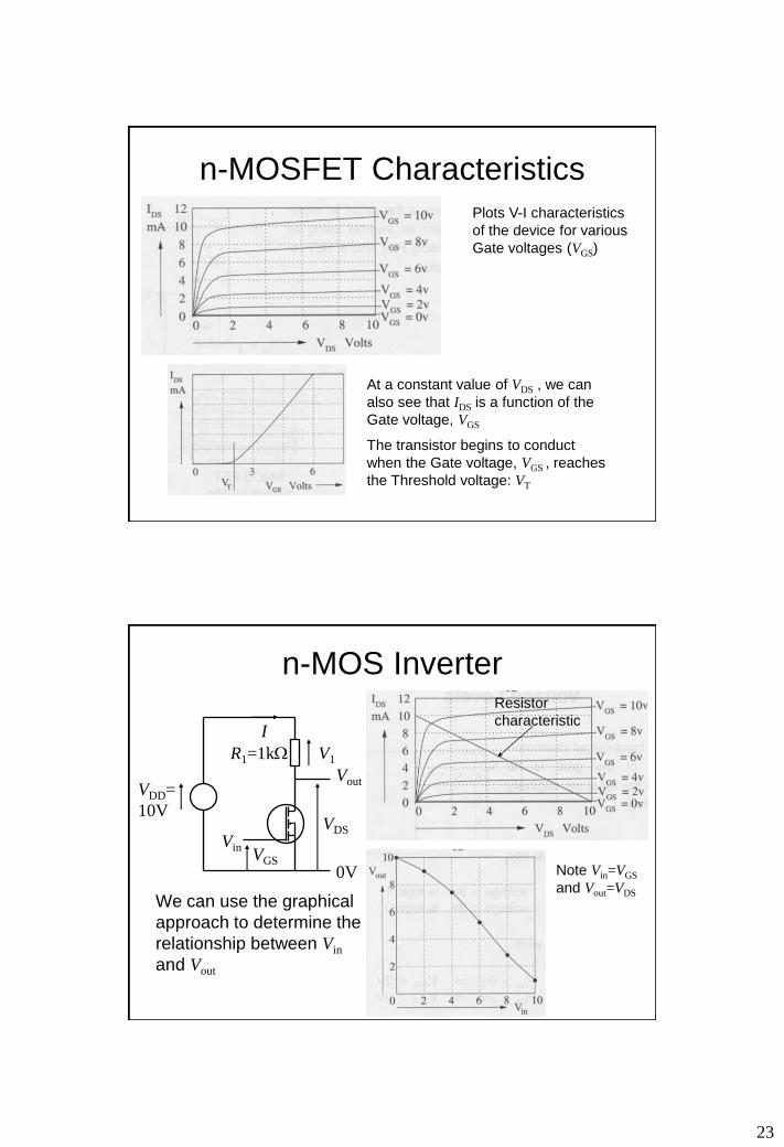
n-MOSFET Characteristics
Plots V-I characteristics
of the device for various
Gate voltages (VGS)
At a constant value of VDS , we can
also see that IDS is a function of the
Gate voltage, VGS
The transistor begins to conduct
when the Gate voltage, VGS , reaches
the Threshold voltage: VT
n-MOS Inverter
VDD=
10V
R1=1kW
I
Vout
V1
VDS
0V VGS
Vin
We can use the graphical
approach to determine the
relationship between Vin
and Vout
Note Vin=VGS
and Vout=VDS
Resistor
characteristic
24
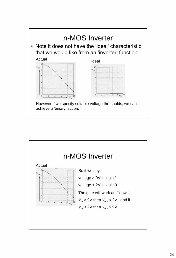
n-MOS Inverter • Note it does not have the ‘ideal’ characteristic
that we would like from an ‘inverter’ function
Actual Ideal
However if we specify suitable voltage thresholds, we can
achieve a ‘binary’ action.
n-MOS Inverter Actual
So if we say:
voltage > 9V is logic 1
voltage < 2V is logic 0
The gate will work as follows:
Vin > 9V then Vout < 2V and if
Vin < 2V then Vout > 9V
25
n-MOS Logic
• It is possible (and was done in the early days)
to build other logic functions, e.g., NOR and
NAND using n-MOS transistors
• However, n-MOS logic has fundamental
problems:
– Speed of operation
– Power consumption
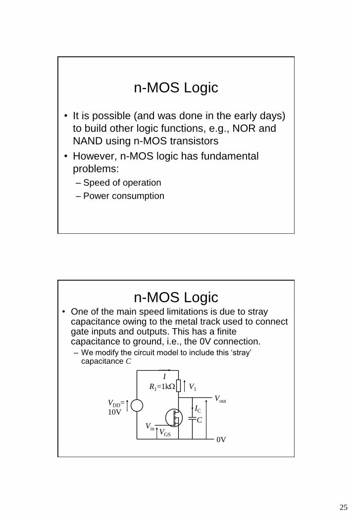
n-MOS Logic • One of the main speed limitations is due to stray
capacitance owing to the metal track used to connect gate inputs and outputs. This has a finite capacitance to ground, i.e., the 0V connection. – We modify the circuit model to include this ‘stray’
capacitance C
VDD=
10V
R1=1kW
I
Vout
V1
0V VGS
Vin
C
IC
26
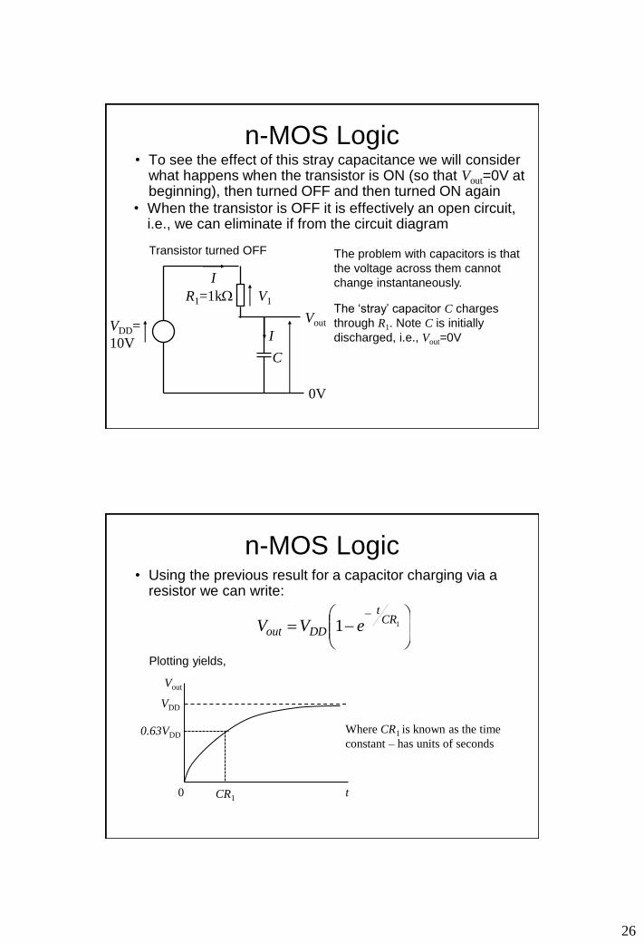
n-MOS Logic • To see the effect of this stray capacitance we will consider
what happens when the transistor is ON (so that Vout=0V at beginning), then turned OFF and then turned ON again
The problem with capacitors is that
the voltage across them cannot
change instantaneously.
VDD=
10V
R1=1kW
I
Vout
V1
0V
C
I
The ‘stray’ capacitor C charges
through R1. Note C is initially
discharged, i.e., Vout=0V
Transistor turned OFF
• When the transistor is OFF it is effectively an open circuit, i.e., we can eliminate if from the circuit diagram
n-MOS Logic
Plotting yields,
11
CRt
DDout eVV
Vout
t 0
VDD
0.63VDD
CR1
Where CR1 is known as the time
constant – has units of seconds
• Using the previous result for a capacitor charging via a resistor we can write:
27
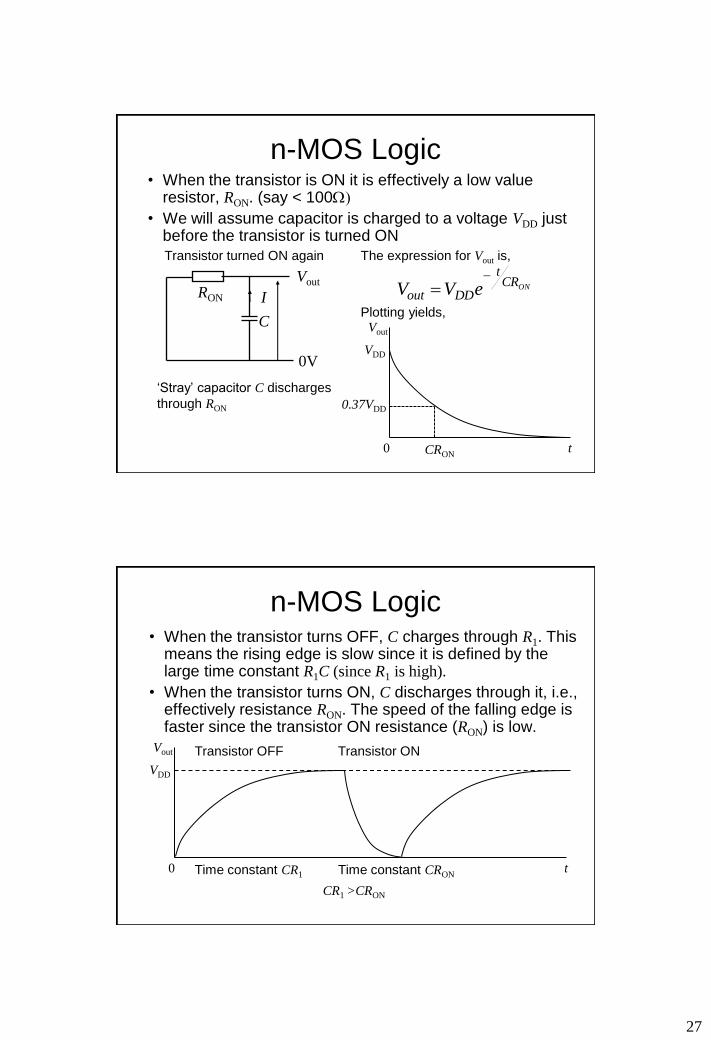
n-MOS Logic
Vout
‘Stray’ capacitor C discharges
through RON
Transistor turned ON again
• When the transistor is ON it is effectively a low value resistor, RON. (say < 100W)
• We will assume capacitor is charged to a voltage VDD just before the transistor is turned ON
RON
0V
C
I
The expression for Vout is,
ONCRt
DDout eVV
Plotting yields, Vout
t 0
VDD
0.37VDD
CRON
n-MOS Logic • When the transistor turns OFF, C charges through R1. This
means the rising edge is slow since it is defined by the large time constant R1C (since R1 is high).
• When the transistor turns ON, C discharges through it, i.e., effectively resistance RON. The speed of the falling edge is faster since the transistor ON resistance (RON) is low.
Vout
t 0
VDD
Time constant CR1
Transistor OFF Transistor ON
Time constant CRON
CR1 >CRON
28
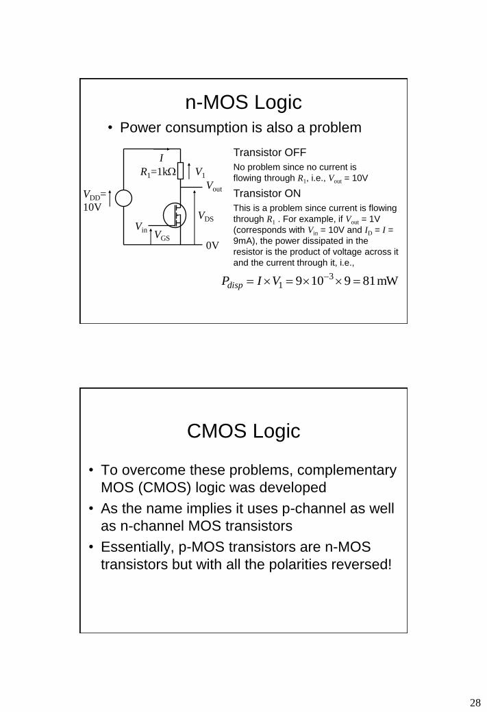
n-MOS Logic
• Power consumption is also a problem
VDD=
10V
R1=1kW
I
Vout
V1
VDS
0V VGS
Vin
Transistor OFF
No problem since no current is
flowing through R1, i.e., Vout = 10V
Transistor ON
This is a problem since current is flowing
through R1 . For example, if Vout = 1V
(corresponds with Vin = 10V and ID = I =
9mA), the power dissipated in the
resistor is the product of voltage across it
and the current through it, i.e.,
mW 819109 31 VIPdisp
CMOS Logic
• To overcome these problems, complementary
MOS (CMOS) logic was developed
• As the name implies it uses p-channel as well
as n-channel MOS transistors
• Essentially, p-MOS transistors are n-MOS
transistors but with all the polarities reversed!
29
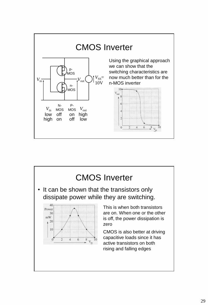
CMOS Inverter
VSS=
10V Vout Vin
p-
MOS
n-
MOS
Vin
N-
MOS
P-
MOS Vout
low off on high high on low off
Using the graphical approach
we can show that the
switching characteristics are
now much better than for the
n-MOS inverter
CMOS Inverter
• It can be shown that the transistors only
dissipate power while they are switching.
This is when both transistors
are on. When one or the other
is off, the power dissipation is
zero
CMOS is also better at driving
capacitive loads since it has
active transistors on both
rising and falling edges
30
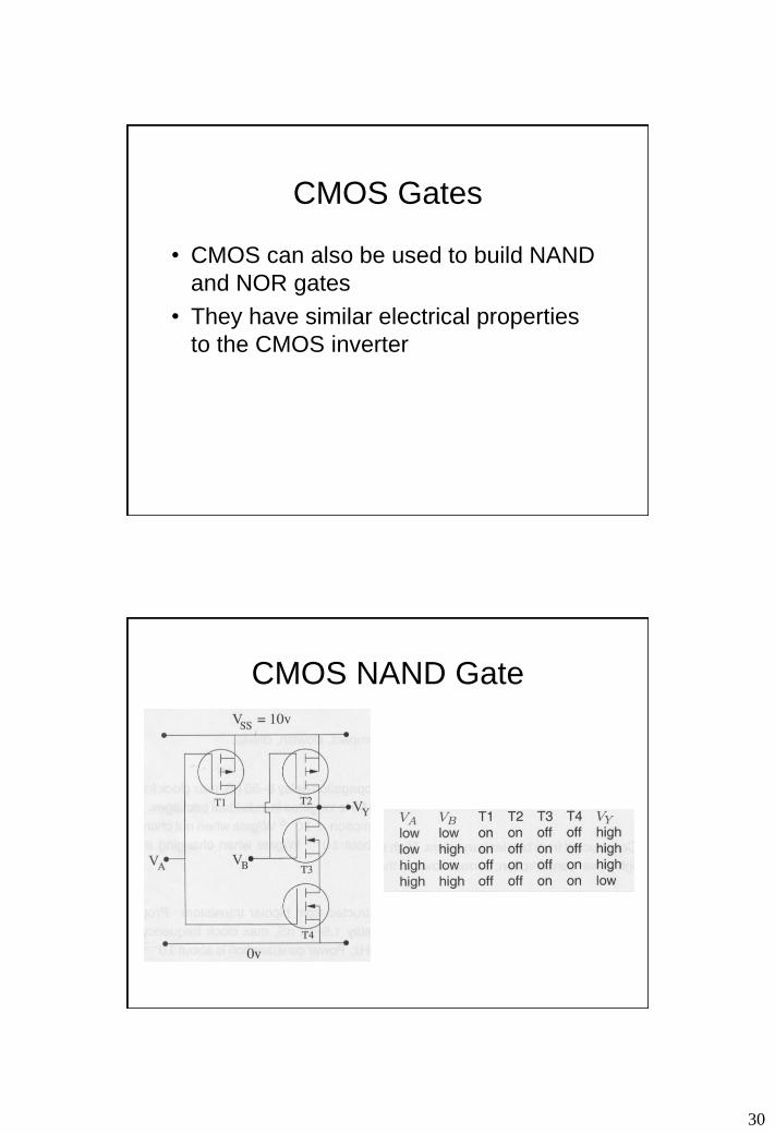
CMOS Gates
• CMOS can also be used to build NAND
and NOR gates
• They have similar electrical properties
to the CMOS inverter
CMOS NAND Gate
31
Logic Families
• NMOS – compact, slow, cheap, obsolete
• CMOS – Older families slow (4000 series about 60ns), but new ones (74AC) much faster (3ns). 74HC series popular
• TTL – Uses bipolar transistors. Known as 74 series. Note that most 74 series devices are now available in CMOS. Older versions slow (LS about 16ns), newer ones faster (AS about 2ns)
• ECL – High speed, but high power consumption
Logic Families
• Best to stick with the particular family which has the best performance, power consumption cost trade-off for the required purpose
• It is possible to mix logic families and sub-families, but care is required regarding the acceptable logic voltage levels and gate current handling capabilities
32
Meaning of Voltage Levels
• As we have seen, the relationship between
the input voltage to a gate and the output
voltage depends upon the particular
implementation technology
• Essentially, the signals between outputs and
inputs are ‘analogue’ and so are susceptible
to corruption by additive noise, e.g., due to
cross talk from signals in adjacent wires
• What we need is a method for quantifying the
tolerance of a particular logic to noise
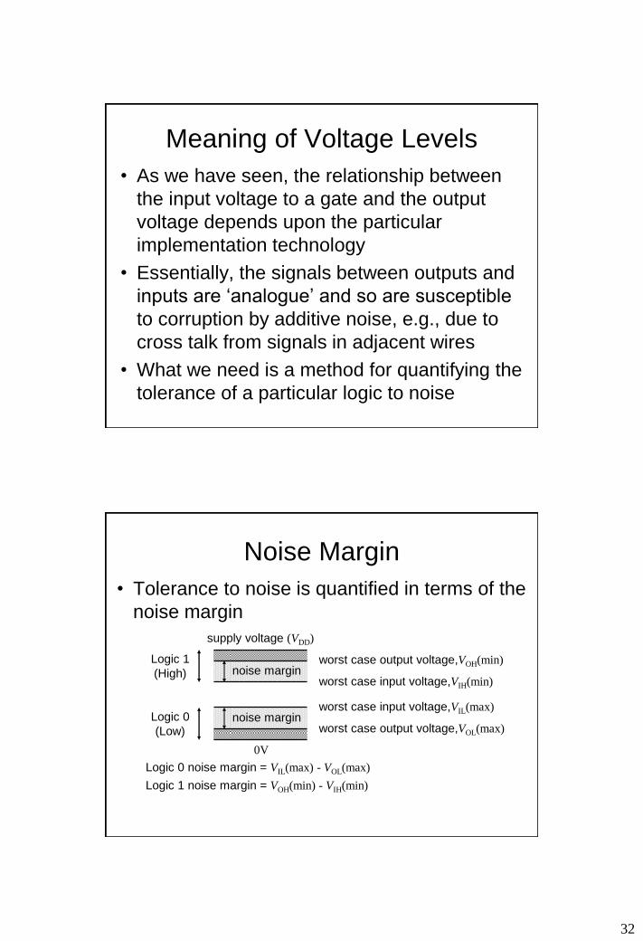
Noise Margin
• Tolerance to noise is quantified in terms of the
noise margin
0V
supply voltage (VDD)
worst case input voltage,VIL(max)
worst case output voltage,VOL(max) noise margin
worst case input voltage,VIH(min)
worst case output voltage,VOH(min) noise margin
Logic 1
(High)
Logic 0
(Low)
Logic 0 noise margin = VIL(max) - VOL(max)
Logic 1 noise margin = VOH(min) - VIH(min)

33
Noise Margin
• For the 74 series High Speed CMOS (HCMOS) used in the hardware labs (using the values from the data sheet):
Logic 0 noise margin = VIL(max) - VOL(max)
Logic 0 noise margin = 1.35 – 0.1 = 1.25 V
Logic 1 noise margin = VOH(min) - VIH(min)
Logic 1 noise margin = 4.4 – 3.15 = 1.25 V
See the worst case noise margin = 1.25V, which is much
greater than the 0.4 V typical of TTL series devices.
Consequently HCMOS devices can tolerate more noise pick-
up before performance becomes compromised


