reach optical interconnect in data centersDesign of distributed amplifier structures for short
Academic year 2018-2019
Master of Science in Electrical Engineering - main subject Electronic Circuits and Systems
Master's dissertation submitted in order to obtain the academic degree of
Ir. Hannes Ramon, Prof. dr. ir. Guy TorfsCounsellors: Dr. ir. Peter Ossieur, Ir. Laurens Breyne, Ir. Michael Vanhoecke,Supervisors: Prof. dr. ir. Johan Bauwelinck, Prof. dr. ir. Guy Torfs
Student number: 01405466
Tinus Pannier


PrefaceThis master’s dissertation is the conclusion of my engineering degree, andI hereby want to seize the opportunity to thank all of the professors andteachers who have selflessly shared their knowledge with me over thepast years.
One year ago, I was welcomed at the Intec Design research group by prof.dr. ir. Johan Bauwelinck. I want to thank prof. Johan Bauwelinck and theentire research group for creating a motivating environment where I wasgiven the chance to carry out my master’s thesis. In particular, I want tothank dr. ir. Peter Ossieur for introducing me to the subject of this disser-tation, and for exploring the possibilities of continuing this project. Thisthesis would not have been the same without the input of prof. dr. ir. GuyTorfs, who shared his endless knowledge and for which I am very grateful.Furthermore, I want to thank ir. Michael Vanhoecke for introducing me tothe lab equipment and dr. ir. Bart Moeneclaey for solving ICT problems.Last, but in no way least, I want to express my deepest gratitude towardsir. Hannes Ramon for guiding me through this year, for introducing me toCadence, for helping me out in the lab, for coming to my aid whenever Ineeded it, and for proofreading this text. Thank you, Hannes.
I would like to thank my parents, Veerle and Jan, for their support thesepast five years, and my brother Stan and my cousin Rosa for proofreadingthis text.
Sharing the thesis room with my fellow students Louise Catthoor,Muhammad Qamar, Jacques Van Damme and Achim Vandierendonckwas a real pleasure, and I wish them the best of luck. Finally, I want tothank my friends of the 8-team for offering distraction when it was mostwelcome.
Tinus Pannier, May 30, 2019
vii


Admission to Loan
De auteur geeft de toelating deze masterproef voor consultatie beschikbaarte stellen en delen van de masterproef te kopieren voor persoonlijk gebruik.Elk ander gebruik valt onder de bepalingen van het auteursrecht, in hetbijzonder met betrekking tot de verplichting de bron uitdrukkelijk tevermelden bij het aanhalen van resultaten uit deze masterproef.
The author gives permission to make this master dissertation availablefor consultation and to copy parts of this master dissertation for personaluse. In all cases of other use, the copyright terms have to be respected, inparticular with regard to the obligation to state explicitly the source whenquoting results from this master dissertation.
Tinus Pannier, May 30, 2019
ix

Design of distributed amplifier structures forshort reach optical interconnect in data centers
Tinus PannierStudent number: 01405466
Master’s dissertation submitted in order to obtain the academic degree ofMaster of Science in Electrical Engineering - main subject Electronic
Circuits and Systems
Academic year 2018–2019
Supervisors: Prof. dr. ir. Johan Bauwelinck, Prof. dr. ir. Guy TorfsCounsellors: Dr. ir. Peter Ossieur, Ir. Laurens Breyne, Ir. Michael
Vanhoecke, Ir. Hannes Ramon, Prof. dr. ir. Guy Torfs
Faculty of Engineering and ArchitectureGhent University
Summary
Data centers rely on optical transceivers to establish fast intra data centernetworks. This master’s dissertation focuses on the optical modulatordriver. This amplifier, preferably implemented in a sub-micron CMOStechnology to allow integration with microprocessors, should have a largebandwidth and should be resistant to the large voltage swing required bythe optical modulator. The distributed amplifier topology is able to deliverthe required bandwidth, and is the subject of this master’s dissertation.A CMOS distributed amplifier was designed, ultimately achieving a band-width of 60 GHz with a gain of 19 dB. Eye diagram simulations sug-gest error-free operation at 2 VPP 80 GBaud PAM4. This performance wasachieved by making extensive use of electromagnetic simulations to verifythe behavior of integrated inductors.
Keywords
Distributed amplifier, Optical modulator driver, Analog circuit design,Fiber-optic links and networks, mmWave RF design
xi

Design of Distributed Amplifier Structures for Short
Reach Optical Interconnect in Data Centers
Tinus Pannier
Prof. dr. ir. Johan Bauwelinck, Prof. dr. ir. Guy Torfs, Dr. ir. Peter Ossieur, Ir. Laurens Breyne, Ir. Michael
Vanhoecke, Ir. Hannes Ramon
Abstract-Data centers make use of optical transceivers to
establish fast intra data center networks. This master’s
dissertation studies the design of a 28nm FDSOI CMOS
distributed amplifier that is suitable for driving an optical
modulator. Extensive use was made of electromagnetic (EM)
simulations to characterize and verify the performance of
integrated inductors. Stacked cascode circuits are used to
distribute the large output voltage swing over multiple transistors,
thereby preventing breakdown of the sub-micron devices. An
iterative design procedure is presented to optimize the sizing of the
inductors for the chosen transconductance stages. Simulations
show that the designed distributed amplifier achieves a gain of
19dB over a bandwidth of 60GHz, with matching better than
-13dB over the entire frequency range. Eye diagrams suggest
error-free operation at 2VPP 80GBaud PAM4.
Keywords-distributed amplifier, optical modulator driver,
analog circuit design, fiber-optic links and networks, mmWave
RF design
I. INTRODUCTION
Internet applications such as e-commerce, video streaming
services, etc. rely on large data centers. These data centers use
optical transceivers to establish fast communication links in the
intra data center network. This article focuses on the transmitter
side of the optical transceiver, more specifically the amplifier
which drives the optical modulator. To meet the increasing
demand for higher bit rates, this driver should have a bandwidth
in excess of 30GHz. Moreover, this driver, implemented in a
sub-micron CMOS technology to allow integration with
microprocessors or FPGAs, should be able to withstand the
large voltage swing required by the optical modulator. A
distributed amplifier with a gain of 20dB will be designed to
meet the above specifications. This amplifier consists of 6
transconductance stages, which are discussed in the next
section. Section III considers the design of the inductors
interconnecting these stages. Inductors and transconductance
stages are combined in the design procedure outlined in Section
IV. Section V presents simulation results to confirm the
operation of the amplifier. Finally, a conclusion is drawn in
Section VI.
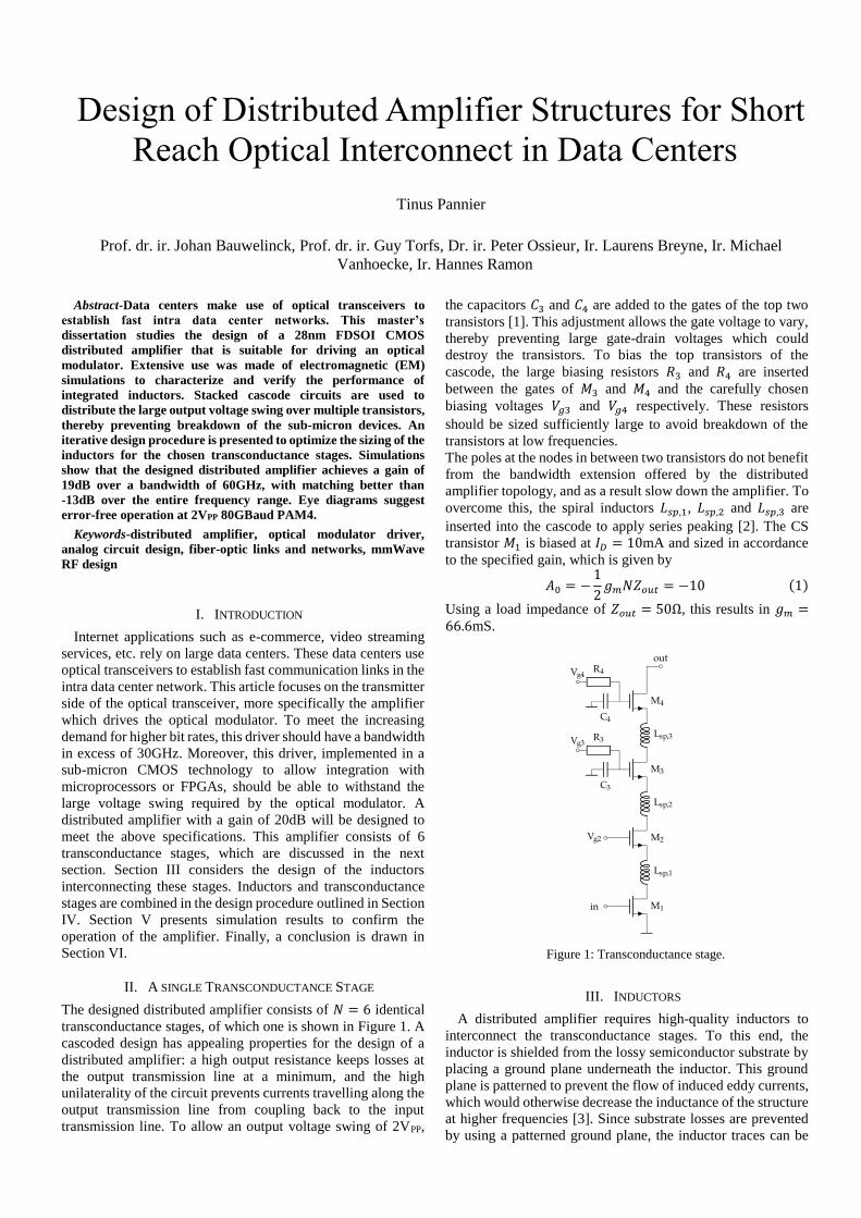
II. A SINGLE TRANSCONDUCTANCE STAGE
The designed distributed amplifier consists of 𝑁 = 6 identical
transconductance stages, of which one is shown in Figure 1. A
cascoded design has appealing properties for the design of a
distributed amplifier: a high output resistance keeps losses at
the output transmission line at a minimum, and the high
unilaterality of the circuit prevents currents travelling along the
output transmission line from coupling back to the input
transmission line. To allow an output voltage swing of 2VPP,
the capacitors 𝐶3 and 𝐶4 are added to the gates of the top two
transistors [1]. This adjustment allows the gate voltage to vary,
thereby preventing large gate-drain voltages which could
destroy the transistors. To bias the top transistors of the
cascode, the large biasing resistors 𝑅3 and 𝑅4 are inserted
between the gates of 𝑀3 and 𝑀4 and the carefully chosen
biasing voltages 𝑉𝑔3 and 𝑉𝑔4 respectively. These resistors
should be sized sufficiently large to avoid breakdown of the
transistors at low frequencies.
The poles at the nodes in between two transistors do not benefit
from the bandwidth extension offered by the distributed
amplifier topology, and as a result slow down the amplifier. To
overcome this, the spiral inductors 𝐿𝑠𝑝,1, 𝐿𝑠𝑝,2 and 𝐿𝑠𝑝,3 are
inserted into the cascode to apply series peaking [2]. The CS
transistor 𝑀1 is biased at 𝐼𝐷 = 10mA and sized in accordance
to the specified gain, which is given by
𝐴0 = −1
2𝑔𝑚𝑁𝑍𝑜𝑢𝑡 = −10 (1)
Using a load impedance of 𝑍𝑜𝑢𝑡 = 50Ω, this results in 𝑔𝑚 =66.6mS.
III. INDUCTORS
A distributed amplifier requires high-quality inductors to
interconnect the transconductance stages. To this end, the
inductor is shielded from the lossy semiconductor substrate by
placing a ground plane underneath the inductor. This ground
plane is patterned to prevent the flow of induced eddy currents,
which would otherwise decrease the inductance of the structure
at higher frequencies [3]. Since substrate losses are prevented
by using a patterned ground plane, the inductor traces can be
Figure 1: Transconductance stage.
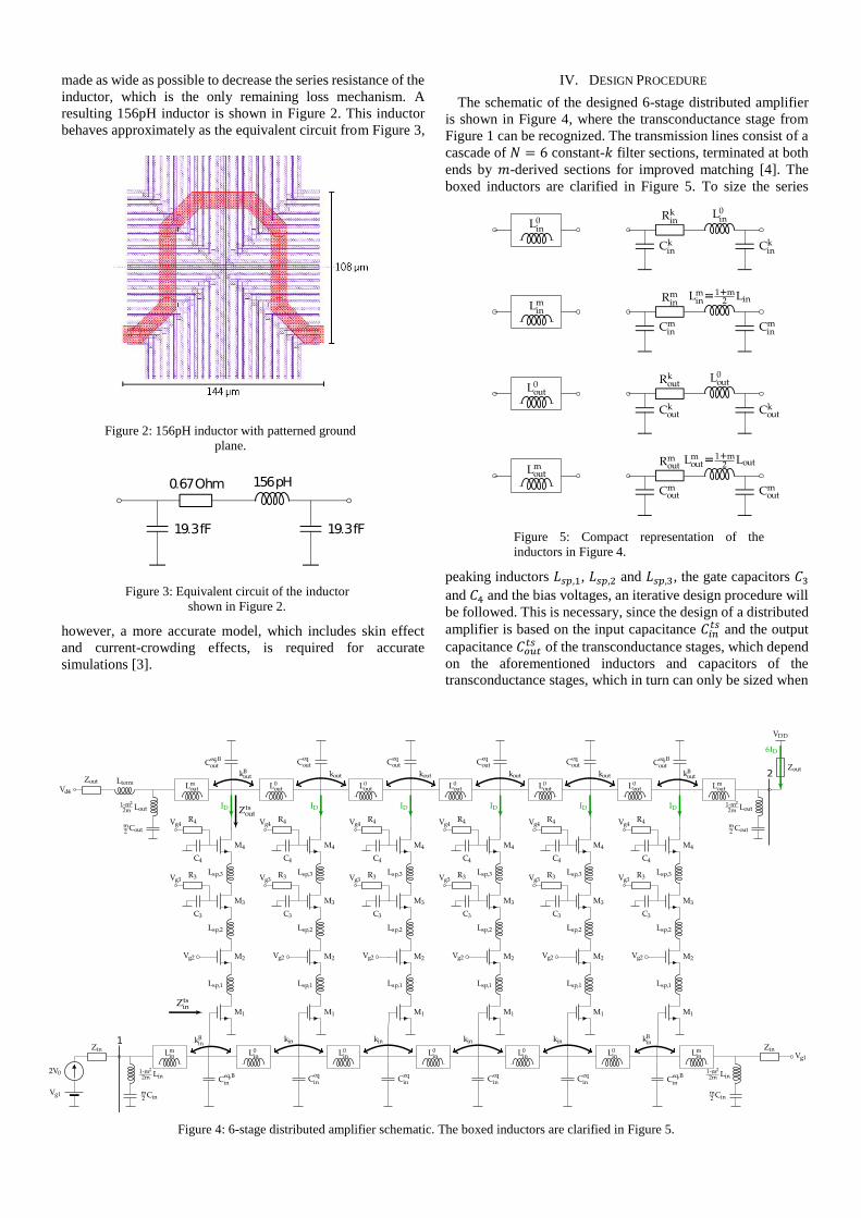
made as wide as possible to decrease the series resistance of the
inductor, which is the only remaining loss mechanism. A
resulting 156pH inductor is shown in Figure 2. This inductor
behaves approximately as the equivalent circuit from Figure 3,
however, a more accurate model, which includes skin effect
and current-crowding effects, is required for accurate
simulations [3].
IV. DESIGN PROCEDURE
The schematic of the designed 6-stage distributed amplifier
is shown in Figure 4, where the transconductance stage from
Figure 1 can be recognized. The transmission lines consist of a
cascade of 𝑁 = 6 constant-𝑘 filter sections, terminated at both
ends by 𝑚-derived sections for improved matching [4]. The
boxed inductors are clarified in Figure 5. To size the series
peaking inductors 𝐿𝑠𝑝,1, 𝐿𝑠𝑝,2 and 𝐿𝑠𝑝,3, the gate capacitors 𝐶3
and 𝐶4 and the bias voltages, an iterative design procedure will
be followed. This is necessary, since the design of a distributed
amplifier is based on the input capacitance 𝐶𝑖𝑛𝑡𝑠 and the output
capacitance 𝐶𝑜𝑢𝑡𝑡𝑠 of the transconductance stages, which depend
on the aforementioned inductors and capacitors of the
transconductance stages, which in turn can only be sized when
Figure 3: Equivalent circuit of the inductor
shown in Figure 2.
Figure 2: 156pH inductor with patterned ground
plane.
Figure 5: Compact representation of the
inductors in Figure 4.
Figure 4: 6-stage distributed amplifier schematic. The boxed inductors are clarified in Figure 5.
the entire amplifier is considered. The design procedure
consists of 5 steps and is outlined below.
1) Step 1: Input capacitance
Determine the input capacitance 𝐶𝑖𝑛𝑡𝑠 and the output
capacitance 𝐶𝑜𝑢𝑡𝑡𝑠 of a transconductance stage (indicated by 𝑍𝑖𝑛
𝑡𝑠
and 𝑍𝑜𝑢𝑡𝑡𝑠 in Figure 4), using an educated guess for the initial
values of 𝐿𝑠𝑝,1, 𝐿𝑠𝑝,2, 𝐿𝑠𝑝,3, 𝐶3, 𝐶4, 𝑅3, 𝑅4 and the biasing
voltages.
2) Step 2: Inductor sizing
Every node of the input transmission line should have a total
capacitance of 𝐶𝑖𝑛, and similarly every node of the output
transmission line should have a total capacitance of 𝐶𝑜𝑢𝑡.
Identifying with the circuits in Figure 4 and Figure 5, this is
expressed as
𝐶𝑖𝑛𝑡𝑠 + 𝐶𝑖𝑛
𝑒𝑞,𝐵+ 𝐶𝑖𝑛
𝑘 + 𝐶𝑖𝑛𝑚 = 𝐶𝑖𝑛 (2)
𝐶𝑖𝑛𝑡𝑠 + 𝐶𝑖𝑛
𝑒𝑞+ 2𝐶𝑖𝑛
𝑘 = 𝐶𝑖𝑛 (3)
𝐶𝑜𝑢𝑡𝑡𝑠 + 𝐶𝑜𝑢𝑡
𝑒𝑞,𝐵+ 𝐶𝑜𝑢𝑡
𝑘 + 𝐶𝑜𝑢𝑡𝑚 = 𝐶𝑜𝑢𝑡 (4)
𝐶𝑜𝑢𝑡𝑡𝑠 + 𝐶𝑜𝑢𝑡
𝑒𝑞+ 2𝐶𝑜𝑢𝑡
𝑘 = 𝐶𝑜𝑢𝑡 (5)
Unintentional inductive coupling between adjacent inductors
will be neglected for now. This is expressed by setting 𝑘𝑖𝑛 =𝑘𝑖𝑛
𝐵 = 𝑘𝑜𝑢𝑡 = 𝑘𝑜𝑢𝑡𝐵 = 0, resulting in 𝐿𝑜𝑢𝑡 = 𝐿𝑜𝑢𝑡
0 . To size the
series inductors of the constant-𝑘 sections in the output TL, we
set
𝑍𝑜𝑢𝑡 = √𝐿𝑜𝑢𝑡
𝐶𝑜𝑢𝑡
= √𝐿𝑜𝑢𝑡
0
𝐶𝑜𝑢𝑡𝑡𝑠 + 𝐶𝑜𝑢𝑡
𝑒𝑞+ 2𝐶𝑜𝑢𝑡
𝑘 = 50Ω (6)
The optimal solution will be the one resulting in the smallest
inductor 𝐿𝑜𝑢𝑡0 , because this inductor will have the smallest
series resistance. To get to this optimal solution, we can put
𝐶𝑜𝑢𝑡𝑒𝑞
= 0, and carefully tune the inductor until it fits the
equation. The inductor from Figure 3 fits (6) for the initial
sizing of the transconductance stage with 𝐶𝑜𝑢𝑡𝑡𝑠 = 23.7fF.
The situation at the outer ends of the transmission line is
somewhat different, since the series inductors of the 𝑚-derived
sections 𝐿𝑜𝑢𝑡𝑚 are smaller, and as a result also have less parasitic
capacitance: 𝐶𝑜𝑢𝑡𝑚 < 𝐶𝑜𝑢𝑡
𝑘 . This can be compensated by sizing
𝐶𝑜𝑢𝑡𝑒𝑞,𝐵
according to (4).
To size the inductors of the input transmission line, phase
matching is imposed:
𝐿𝑖𝑛𝐶𝑖𝑛 = 𝐿𝑜𝑢𝑡𝐶𝑜𝑢𝑡 (7)
or equivalently, using (3) and 𝐿𝑖𝑛 = 𝐿𝑖𝑛0 (no inductive
coupling):
𝐿𝑖𝑛0 (𝐶𝑖𝑛
𝑡𝑠 + 𝐶𝑖𝑛𝑒𝑞
+ 2𝐶𝑖𝑛𝑘 ) = 𝐿𝑜𝑢𝑡𝐶𝑜𝑢𝑡 (8)
The designed inductor which fits (8) for 𝐶𝑖𝑛𝑒𝑞
= 0 is
characterized by 𝐶𝑖𝑛𝑘 = 12.9fF and 𝐿𝑖𝑛
0 = 109pH, using 𝐶𝑖𝑛𝑡𝑠 =
64.0fF of the initial sizing of the transconductance stage. It is
again necessary to size 𝐶𝑖𝑛𝑒𝑞,𝐵
> 0 (see (2)) to compensate for
the smaller 𝑚-derived series inductors. The designed amplifier
has an input impedance given by
𝑍𝑖𝑛 = √𝐿𝑖𝑛
𝐶𝑖𝑛
= 35Ω (9)
3) Step 3: S-parameter simulations
S-parameter simulations are performed to verify the
performance of the designed amplifier. Attention should be
paid at the amount of peaking in the 𝑆21 transfer function. This
peaking can be controlled by tuning the inductors 𝐿𝑠𝑝,1, 𝐿𝑠𝑝,2
and 𝐿𝑠𝑝,3. However, by doing so, the parasitic capacitance of
these inductors will change, and as a consequence the input
capacitance 𝐶𝑖𝑛𝑡𝑠 and output capacitance 𝐶𝑜𝑢𝑡
𝑡𝑠 of the
transconductance stage will also change. As such, Step 1
through Step 3 should be repeated until 𝐶𝑖𝑛𝑡𝑠 and 𝐶𝑜𝑢𝑡
𝑡𝑠 no longer
change.
4) Step 4: Voltage swing over the cascode transistors
The output voltage swing of 2VPP can be safely distributed
over the cascode transistors through an appropriate sizing of the
gate capacitors 𝐶3 and 𝐶4, and the gate biasing voltages. Any
change in 𝐶3 and 𝐶4 will result in different values of 𝐶𝑖𝑛𝑡𝑠 and
𝐶𝑜𝑢𝑡𝑡𝑠 , demanding a repeat of Step 1 through Step 4 until 𝐶𝑖𝑛
𝑡𝑠 and
𝐶𝑜𝑢𝑡𝑡𝑠 no longer change.
5) Step 5: Inductive coupling between adjacent
inductors
Unintentional inductive coupling between adjacent inductors
can be taken into account by including the coupling coefficients
𝑘𝑖𝑛, 𝑘𝑜𝑢𝑡, 𝑘𝑖𝑛𝐵 and 𝑘𝑜𝑢𝑡
𝐵 into the design. The effective input
inductance 𝐿𝑖𝑛 and the effective output inductance 𝐿𝑜𝑢𝑡 can be
defined as
𝐿𝑖𝑛 = (1 + 2𝑘𝑖𝑛)𝐿𝑖𝑛0 (10)
𝐿𝑜𝑢𝑡 = (1 + 2𝑘𝑜𝑢𝑡)𝐿𝑜𝑢𝑡0 (11)
and as a result, demand a redesign of the inductors 𝐿𝑖𝑛0 and
𝐿𝑜𝑢𝑡0 [5]. The simplest solution is to maintain the previous
values of 𝐶𝑖𝑛, 𝐿𝑖𝑛, 𝐶𝑜𝑢𝑡 and 𝐿𝑜𝑢𝑡. The redesign of the inductors
𝐿𝑖𝑛0 and 𝐿𝑜𝑢𝑡
0 will result in a decrease of the parasitic
capacitances 𝐶𝑖𝑛𝑘 and 𝐶𝑜𝑢𝑡
𝑘 . This can be compensated by sizing
𝐶𝑖𝑛𝑒𝑞
and 𝐶𝑜𝑢𝑡𝑒𝑞
in according to (3), respectively (5).
V. SIMULATION RESULTS
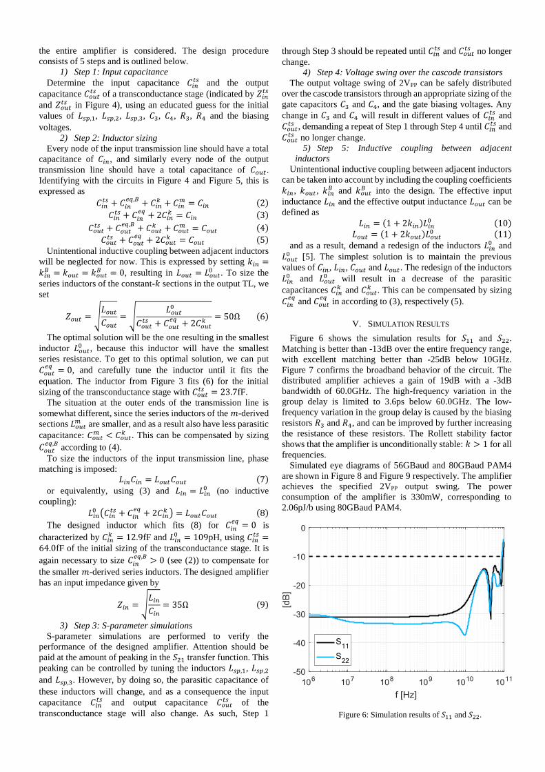
Figure 6 shows the simulation results for 𝑆11 and 𝑆22.
Matching is better than -13dB over the entire frequency range,
with excellent matching better than -25dB below 10GHz.
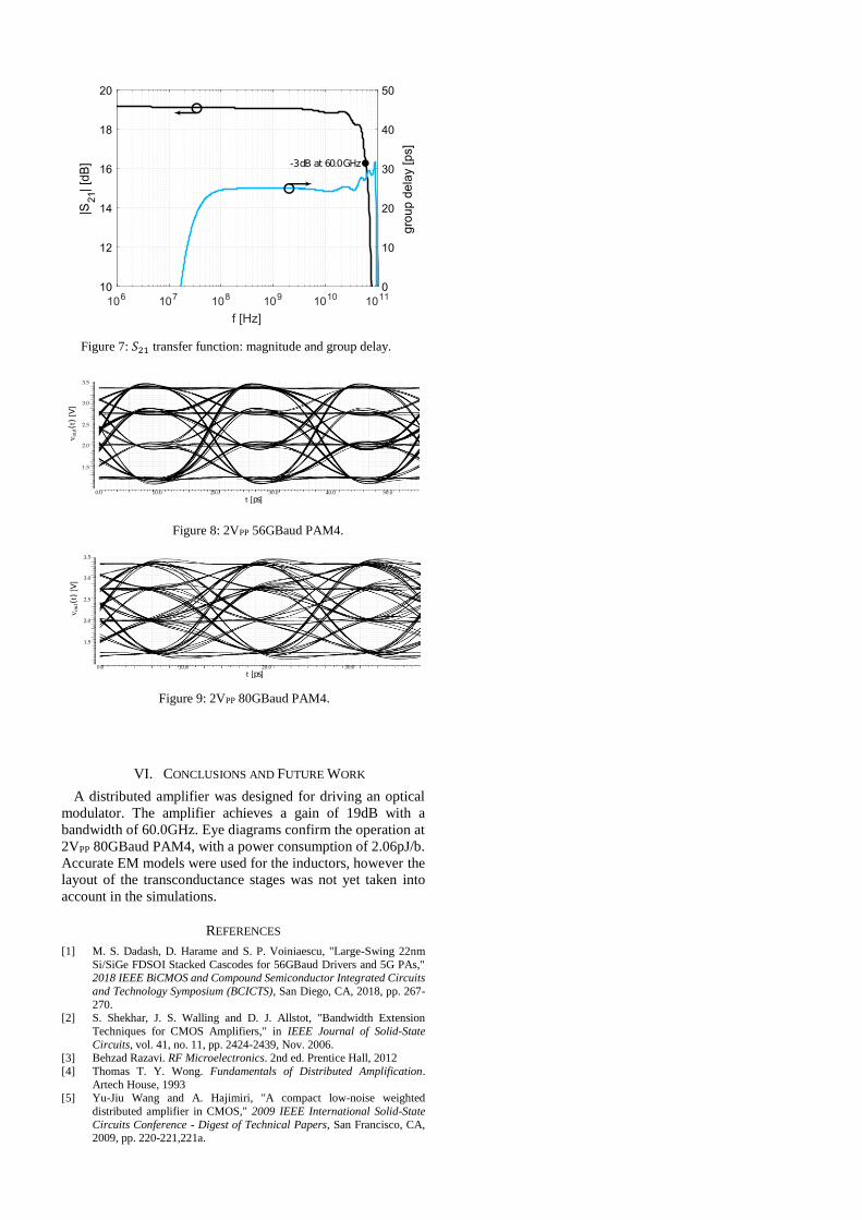
Figure 7 confirms the broadband behavior of the circuit. The
distributed amplifier achieves a gain of 19dB with a -3dB
bandwidth of 60.0GHz. The high-frequency variation in the
group delay is limited to 3.6ps below 60.0GHz. The low-
frequency variation in the group delay is caused by the biasing
resistors 𝑅3 and 𝑅4, and can be improved by further increasing
the resistance of these resistors. The Rollett stability factor
shows that the amplifier is unconditionally stable: 𝑘 > 1 for all
frequencies.
Simulated eye diagrams of 56GBaud and 80GBaud PAM4
are shown in Figure 8 and Figure 9 respectively. The amplifier
achieves the specified 2VPP output swing. The power
consumption of the amplifier is 330mW, corresponding to
2.06pJ/b using 80GBaud PAM4.
Figure 6: Simulation results of 𝑆11 and 𝑆22.
VI. CONCLUSIONS AND FUTURE WORK
A distributed amplifier was designed for driving an optical
modulator. The amplifier achieves a gain of 19dB with a
bandwidth of 60.0GHz. Eye diagrams confirm the operation at
2VPP 80GBaud PAM4, with a power consumption of 2.06pJ/b.
Accurate EM models were used for the inductors, however the
layout of the transconductance stages was not yet taken into
account in the simulations.
REFERENCES
[1] M. S. Dadash, D. Harame and S. P. Voiniaescu, "Large-Swing 22nm
Si/SiGe FDSOI Stacked Cascodes for 56GBaud Drivers and 5G PAs," 2018 IEEE BiCMOS and Compound Semiconductor Integrated Circuits
and Technology Symposium (BCICTS), San Diego, CA, 2018, pp. 267-
270. [2] S. Shekhar, J. S. Walling and D. J. Allstot, "Bandwidth Extension
Techniques for CMOS Amplifiers," in IEEE Journal of Solid-State
Circuits, vol. 41, no. 11, pp. 2424-2439, Nov. 2006. [3] Behzad Razavi. RF Microelectronics. 2nd ed. Prentice Hall, 2012
[4] Thomas T. Y. Wong. Fundamentals of Distributed Amplification.
Artech House, 1993 [5] Yu-Jiu Wang and A. Hajimiri, "A compact low-noise weighted
distributed amplifier in CMOS," 2009 IEEE International Solid-State
Circuits Conference - Digest of Technical Papers, San Francisco, CA, 2009, pp. 220-221,221a.
Figure 7: 𝑆21 transfer function: magnitude and group delay.
Figure 8: 2VPP 56GBaud PAM4.
Figure 9: 2VPP 80GBaud PAM4.

Contents
Preface vii
Admission to Loan ix
Abstract x
Extended Abstract xiii
1. Introduction 11.1. Intuitive description of distributed amplification . . . . . . . 21.2. Goal and outline . . . . . . . . . . . . . . . . . . . . . . . . . 6
2. Theory of Distributed Amplification 92.1. Description based on coupled transmission lines . . . . . . . 92.2. Filter sections based on the image parameter method . . . . 14
2.2.1. Image impedance . . . . . . . . . . . . . . . . . . . . . 142.2.2. Constant-k filter sections . . . . . . . . . . . . . . . . . 152.2.3. m-derived filter sections . . . . . . . . . . . . . . . . . 172.2.4. Distributed amplifier topology . . . . . . . . . . . . . 19
3. Transconductance Stage 233.1. Technology . . . . . . . . . . . . . . . . . . . . . . . . . . . . . 233.2. Modified cascode circuit . . . . . . . . . . . . . . . . . . . . . 24
3.2.1. Biasing . . . . . . . . . . . . . . . . . . . . . . . . . . . 263.2.2. Transistor and capacitor sizing . . . . . . . . . . . . . 27
3.3. Series peaking . . . . . . . . . . . . . . . . . . . . . . . . . . . 29
4. Inductors 314.1. Microstrip as inductor . . . . . . . . . . . . . . . . . . . . . . 314.2. Inductor geometry . . . . . . . . . . . . . . . . . . . . . . . . 33
xvii
Contents
4.3. Equivalent circuit of an on-chip microstrip inductor . . . . . 364.4. Constant-k series inductors . . . . . . . . . . . . . . . . . . . 37
4.4.1. Characterization of an inductor . . . . . . . . . . . . . 384.4.2. Influence of the substrate on the performance of a
distributed amplifier . . . . . . . . . . . . . . . . . . . 404.4.3. Patterned ground plane . . . . . . . . . . . . . . . . . 424.4.4. Series connection of inductors . . . . . . . . . . . . . 45
4.5. Series peaking inductors . . . . . . . . . . . . . . . . . . . . . 48
5. Design of a Distributed Amplifier 515.1. Distributed amplifier topology . . . . . . . . . . . . . . . . . 515.2. Schematic . . . . . . . . . . . . . . . . . . . . . . . . . . . . . 525.3. Design procedure . . . . . . . . . . . . . . . . . . . . . . . . . 56
5.3.1. Step 1: Determine Ctsin and Cts
out . . . . . . . . . . . . . 565.3.2. Step 2: Size the series inductors of the constant-k
and m-derived sections . . . . . . . . . . . . . . . . . 575.3.3. Step 3: Verify the performance of the amplifier through
S-parameter simulation . . . . . . . . . . . . . . . . . 605.3.4. Step 4: Voltage swing over the cascode transistors . . 625.3.5. Step 5: Inductive coupling between adjacent inductors 645.3.6. Time domain simulation results . . . . . . . . . . . . 66
5.4. Layout of a transconductance stage . . . . . . . . . . . . . . . 695.5. Coupling between the input and output transmission lines . 70
6. Conclusions and Future Work 756.1. Results . . . . . . . . . . . . . . . . . . . . . . . . . . . . . . . 756.2. Future work . . . . . . . . . . . . . . . . . . . . . . . . . . . . 76
Bibliography 79
A. Distributed Amplifier Description based on Cascaded 4-portNetworks 85
xviii

List of Abbreviations
CG Common Gate
CS Common Source
DA Distributed Amplifier
EM Electromagnetic
p.u.l. per unit length
PA Power Amplifier
SRF Self-Resonance Frequency
TL Transmission Line
xix


1. Introduction
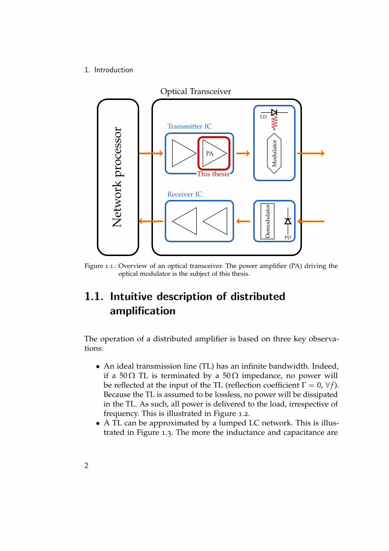
Internet applications such as social media, e-commerce, video streamingservices, document sharing, online gaming, etc. rely on large computingfacilities called data centers. These data centers consist of thousands ofcomputer servers, interconnected via fast fiber-optic links and opticaltransceivers. Due to the increasing popularity of cloud-based applica-tions, these links are put under heavy stress. To meet the demand, onecould propose to simply duplicate all communication links to doublethe available bandwidth. However, this option is not scalable over time,since every new generation will require more rack space and power. Weconclude that faster optical transceivers are required to further increasethe intra data center capacity. These transceivers should be packaged inthe same physical volume as the previous generation and should have acomparable power consumption. Moreover, these transceivers should below-cost, since the amount of deployed devices is very large. This master’sdissertation will focus on the design of a broadband optical transmitter,more specifically the driver circuit which forms the interface between acomputer server and an optical modulator. This is illustrated in Figure 1.1.
The bandwidth of any amplifier is limited by the presence of parasiticcapacitances. Since on-chip inductors have become common, many tech-niques have been devised to further extend the bandwidth of integratedcircuits. The distributed amplifier (DA) concludes this list of bandwidthenhancement techniques. Originally invented by Percival in 1936 andlater elaborated upon by Ginzton in 1948 [3] [12], a distributed amplifierabsorbs the parasitic capacitances of the amplifier stages into artificialtransmission lines, thereby greatly extending the bandwidth of the circuit.In this thesis, a distributed amplifier will be designed that is suitable fordriving optical modulators.
1
1. Introduction
Optical Transceiver
Transmitter IC
PA
Receiver IC
LD
Mod
ulat
or
PDDem
odul
ator
Net
wor
kpr
oces
sor
This thesis
Figure 1.1.: Overview of an optical transceiver. The power amplifier (PA) driving theoptical modulator is the subject of this thesis.
1.1. Intuitive description of distributedamplification
The operation of a distributed amplifier is based on three key observa-tions:
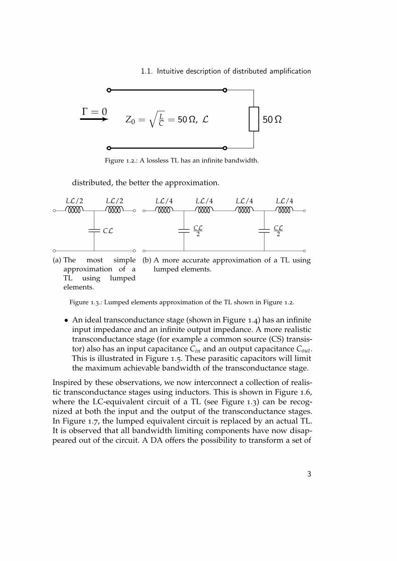
• An ideal transmission line (TL) has an infinite bandwidth. Indeed,if a 50 Ω TL is terminated by a 50 Ω impedance, no power willbe reflected at the input of the TL (reflection coefficient Γ = 0, ∀ f ).Because the TL is assumed to be lossless, no power will be dissipatedin the TL. As such, all power is delivered to the load, irrespective offrequency. This is illustrated in Figure 1.2.• A TL can be approximated by a lumped LC network. This is illus-
trated in Figure 1.3. The more the inductance and capacitance are
2
1.1. Intuitive description of distributed amplification
50 ΩZ0 =√
LC = 50 Ω, L
Γ = 0
Figure 1.2.: A lossless TL has an infinite bandwidth.
distributed, the better the approximation.
LL/2 LL/2
CL
(a) The most simpleapproximation of aTL using lumpedelements.
LL/4 LL/4 LL/4 LL/4
CL2
CL2
(b) A more accurate approximation of a TL usinglumped elements.
Figure 1.3.: Lumped elements approximation of the TL shown in Figure 1.2.
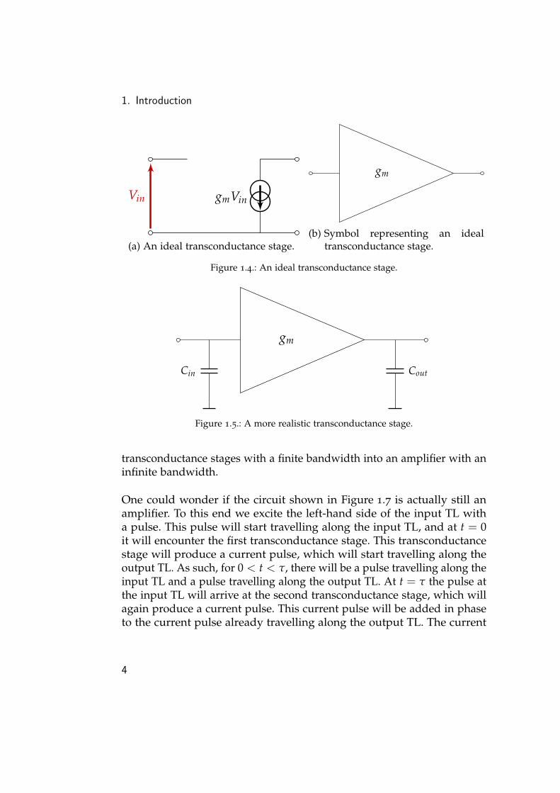
• An ideal transconductance stage (shown in Figure 1.4) has an infiniteinput impedance and an infinite output impedance. A more realistictransconductance stage (for example a common source (CS) transis-tor) also has an input capacitance Cin and an output capacitance Cout.This is illustrated in Figure 1.5. These parasitic capacitors will limitthe maximum achievable bandwidth of the transconductance stage.
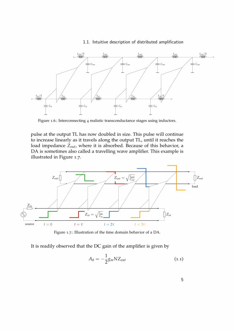
Inspired by these observations, we now interconnect a collection of realis-tic transconductance stages using inductors. This is shown in Figure 1.6,where the LC-equivalent circuit of a TL (see Figure 1.3) can be recog-nized at both the input and the output of the transconductance stages.In Figure 1.7, the lumped equivalent circuit is replaced by an actual TL.It is observed that all bandwidth limiting components have now disap-peared out of the circuit. A DA offers the possibility to transform a set of
3
1. Introduction
gmVinVin
(a) An ideal transconductance stage.
gm
(b) Symbol representing an idealtransconductance stage.
Figure 1.4.: An ideal transconductance stage.
gm
Cin Cout
Figure 1.5.: A more realistic transconductance stage.
transconductance stages with a finite bandwidth into an amplifier with aninfinite bandwidth.
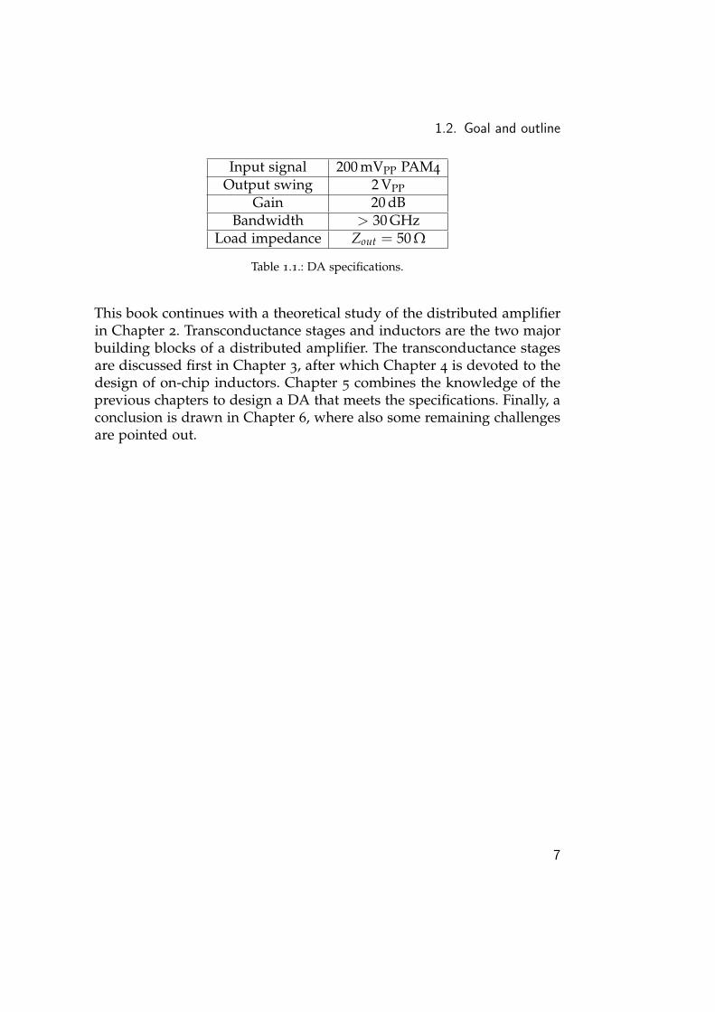
One could wonder if the circuit shown in Figure 1.7 is actually still anamplifier. To this end we excite the left-hand side of the input TL witha pulse. This pulse will start travelling along the input TL, and at t = 0it will encounter the first transconductance stage. This transconductancestage will produce a current pulse, which will start travelling along theoutput TL. As such, for 0 < t < τ, there will be a pulse travelling along theinput TL and a pulse travelling along the output TL. At t = τ the pulse atthe input TL will arrive at the second transconductance stage, which willagain produce a current pulse. This current pulse will be added in phaseto the current pulse already travelling along the output TL. The current
4
1.1. Intuitive description of distributed amplification
Cout
Cin
Cout
Cin
Cout
Cin
Cout
Cin
Lin/2 Lin Lin Lin Lin/2
Lout/2Lout/2 Lout Lout Lout
Figure 1.6.: Interconnecting 4 realistic transconductance stages using inductors.
pulse at the output TL has now doubled in size. This pulse will continueto increase linearly as it travels along the output TL, until it reaches theload impedance Zout, where it is absorbed. Because of this behavior, aDA is sometimes also called a travelling wave amplifier. This example isillustrated in Figure 1.7.
Zin
Zout
Zin =√
LinCin
Zout =√
LoutCout
t = 0 t = τ t = 2τ t = 3τsource
load
Zin
Zout
Figure 1.7.: Illustration of the time domain behavior of a DA.
It is readily observed that the DC gain of the amplifier is given by
A0 = −12
gmNZout (1.1)
5

1. Introduction
where N is the total number of transconductance stages and Zout =√
LoutCout
is the load impedance. Because the output TL is terminated with Zoutat both ends, a factor 1/2 is present in the above formula. To guaranteeoperation as described above, it is essential that the pulses at the input TLand the output TL travel at the same speed. To this end, the phase velocityof the input TL needs to be equal to the phase velocity of the output TL.This is expressed as
1√LinCin
=1√
LoutCout(1.2)
or equivalentlyLinCin = LoutCout (1.3)
The above equation is the so-called phase matching condition of a DA.
1.2. Goal and outline
The goal of this master’s dissertation is to design a distributed amplifierthat is suitable for driving an optical modulator. The amplifier will bedesigned in a sub-micron CMOS technology, to allow for integration withmicroprocessors and network processors. However, optical modulatorsrequire large voltage swings, which could potentially break down the tinytransistors of the advanced CMOS technology. A first challenge will be todesign an amplifier which can provide a large voltage swing, targeting2 VPP, without breaking down any of the transistors. No optical modulatortype will be specified for the design; the load impedance is assumedto be ideal and is given by Zout = 50 Ω. To amplify the weak signalsgenerated by the microprocessors (say 200 mVPP), the amplifier will haveto provide a gain of at least 20 dB (A0 = −10), while operating in itslinear region to support the PAM4 modulation format. The distributedamplifier topology makes it possible to achieve very large bandwidths. Aminimum bandwidth of 30 GHz should be within the reach of this project.The specifications are summarized in Table 1.1.
6
1.2. Goal and outline
Input signal 200 mVPP PAM4Output swing 2 VPP
Gain 20 dBBandwidth > 30 GHz
Load impedance Zout = 50 Ω
Table 1.1.: DA specifications.
This book continues with a theoretical study of the distributed amplifierin Chapter 2. Transconductance stages and inductors are the two majorbuilding blocks of a distributed amplifier. The transconductance stagesare discussed first in Chapter 3, after which Chapter 4 is devoted to thedesign of on-chip inductors. Chapter 5 combines the knowledge of theprevious chapters to design a DA that meets the specifications. Finally, aconclusion is drawn in Chapter 6, where also some remaining challengesare pointed out.
7

2. Theory of DistributedAmplification
This chapter offers two different views on the operation of a distributedamplifier. Section 2.1 starts from a description based on coupled trans-mission lines. This interpretation offers valuable insights and allows toelegantly prove many of the DA design equations. However, this de-scription does not offer a clear recipe on how to design a DA. Anotherapproach which does result in a design methodology is explained inSection 2.2. This description is based on constant-k and m-derived filtersections. A third theoretical description of distributed amplifiers can befound in Appendix A. This description offers a framework for performingcomputations on distributed amplifier structures.
2.1. Description based on coupled transmissionlines
The following derivation is based on [11] [19]. In reality the total transcon-ductance gm,tot is distributed over N discrete transconductance stages.However, at sufficiently low frequencies, it is also possible to regard thetransconductance as being fully distributed over the length of the amplifier.In this case, the transconductance can be represented by a per unit length(p.u.l.) transconductance gm [S/m]. The total transconductance gm,tot isnow given by
gm,tot = gmL (2.1)
where L is the length of the input and output TL. The complete problemis represented in Figure 2.1, where Lin, Cin, Lout and Cout are the p.u.l.
9

2. Theory of Distributed Amplification
2V0
Zin
ZinLin, Cin, L
Zout ZoutLout, Cout, L, gm
0 L z
Vout(0) Vout(L)
Iout(0) Iout(L)
Figure 2.1.: Input and output TL of the DA. The transconductance, characterized bygm[S/m], is uniformely distributed over the complete length of the outputTL.
inductance [H/m] and the p.u.l. capacitance [F/m] of the input andoutput TL respectively. The transmission lines are assumed to be lossless,
and are characterized by their real characteristic impedances Zin =√
LinCin
and Zout =√
LoutCout
. By assuming that the coupling between the input TLand the output TL is unilateral, the voltage and current along the inputTL can directly be written down as
Vin(z) = V0 e−jkinz (2.2)
Iin(z) =V0
Zine−jkinz (2.3)
where kin = ω√
LinCin is the propagation constant of the input TL.
To determine the voltage and current along the output TL, a small sectionof length ∆z of the output TL is shown in Figure 2.2. From this schematic
10
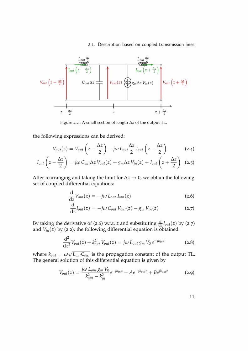
2.1. Description based on coupled transmission lines
Lout∆z2 Lout
∆z2
Cout∆z gm∆z Vin(z)
z− ∆z2 z + ∆z
2z
Vout
(z− ∆z
2
)Vout
(z + ∆z
2
)Vout(z)
Iout
(z− ∆z
2
)Iout
(z + ∆z
2
)
Figure 2.2.: A small section of length ∆z of the output TL.
the following expressions can be derived:
Vout(z) = Vout
(z− ∆z
2
)− jω Lout
∆z2
Iout
(z− ∆z
2
)(2.4)
Iout
(z− ∆z
2
)= jω Cout∆z Vout(z) + gm∆z Vin(z) + Iout
(z +
∆z2
)(2.5)
After rearranging and taking the limit for ∆z→ 0, we obtain the followingset of coupled differential equations:
ddz
Vout(z) = −jω Lout Iout(z) (2.6)
ddz
Iout(z) = −jω Cout Vout(z)− gm Vin(z) (2.7)
By taking the derivative of (2.6) w.r.t. z and substituting ddz Iout(z) by (2.7)
and Vin(z) by (2.2), the following differential equation is obtained
d2
dz2 Vout(z) + k2out Vout(z) = jω Lout gm V0 e−jkinz (2.8)
where kout = ω√
LoutCout is the propagation constant of the output TL.The general solution of this differential equation is given by
Vout(z) =jω Lout gm V0
k2out − k2
ine−jkinz + Ae−jkoutz + Bejkoutz (2.9)
11

2. Theory of Distributed Amplification
where A and B are constants that can be determined from the boundaryconditions. From Figure 2.1, the boundary conditions are readily derivedas
Vout(0) = −Zout Iout(0) (2.10)Vout(L) = Zout Iout(L) (2.11)
From this, A and B are calculated to be
A =j2
gm Zout V0
kin − kout(2.12)
B =−j2
gm V0 Zout
kout + kine−j(kin+kout)L (2.13)
The voltage transfer function of the distributed amplifier can now bedetermined as
Vout(L)V0
= −12
gm Zout je−jkinL − e−jkoutL
kin − kout(2.14)
Because of the presence of both kin and kout in (2.9), this transfer functionshows a 1/ f -behavior at high frequencies. Only in the degenerate casewhere kin = kout, which is equivalent to the phase matching conditionLinCin = LoutCout, the bandwidth will be unlimited. This can be shownby taking the limit for kin → kout, which results in the gain equation of adistributed amplifier:
Vout(L)V0
= −12
gmL Zout e−jkL (2.15)
One could wonder if the left-hand side of the output TL in Figure 2.1shows the same behavior. To this end we calculate
Vout(0)V0
=j2
gm Zout
kin + kout
(1− e−j(kin+kout)L
)(2.16)
which reduces to
Vout(0)V0
= −12
gmL Zout e−jkL sinc (kL) (2.17)
12

2.1. Description based on coupled transmission lines
in the case of phase matching. It is observed that (2.17) only equals (2.15)at low frequencies.
To illustrate the effect of phase matching, Vout(z) is plotted as a functionof z for kout/kin = 1 and kout/kin = 2 and for arbitrary values of the otherconstants describing the problem. The result is shown in Figure 2.3. Fromthis, the following conclusions can be drawn:
• The output voltage increases along the TL. In the case of phasematching, this increase is monotonous.• An amplitude gain of 1
2 gmLZout at z = L is only achieved in the caseof phase matching, as predicted by (2.15).• The gain is minimal at z = 0, as predicted by (2.17).
0.0 0.1 0.2 0.3 0.4 0.5 0.6 0.7 0.8 0.9 1.0
0
0.2
0.4
0.6
0.8
1k
out/k
in = 1
kout
/kin
= 2
zL
|Vout(z)|12 gmLZoutV0
Figure 2.3.: Vout(z) as a function of z for kout/kin = 1 and kout/kin = 2.
13
2. Theory of Distributed Amplification
2.2. Filter sections based on the imageparameter method
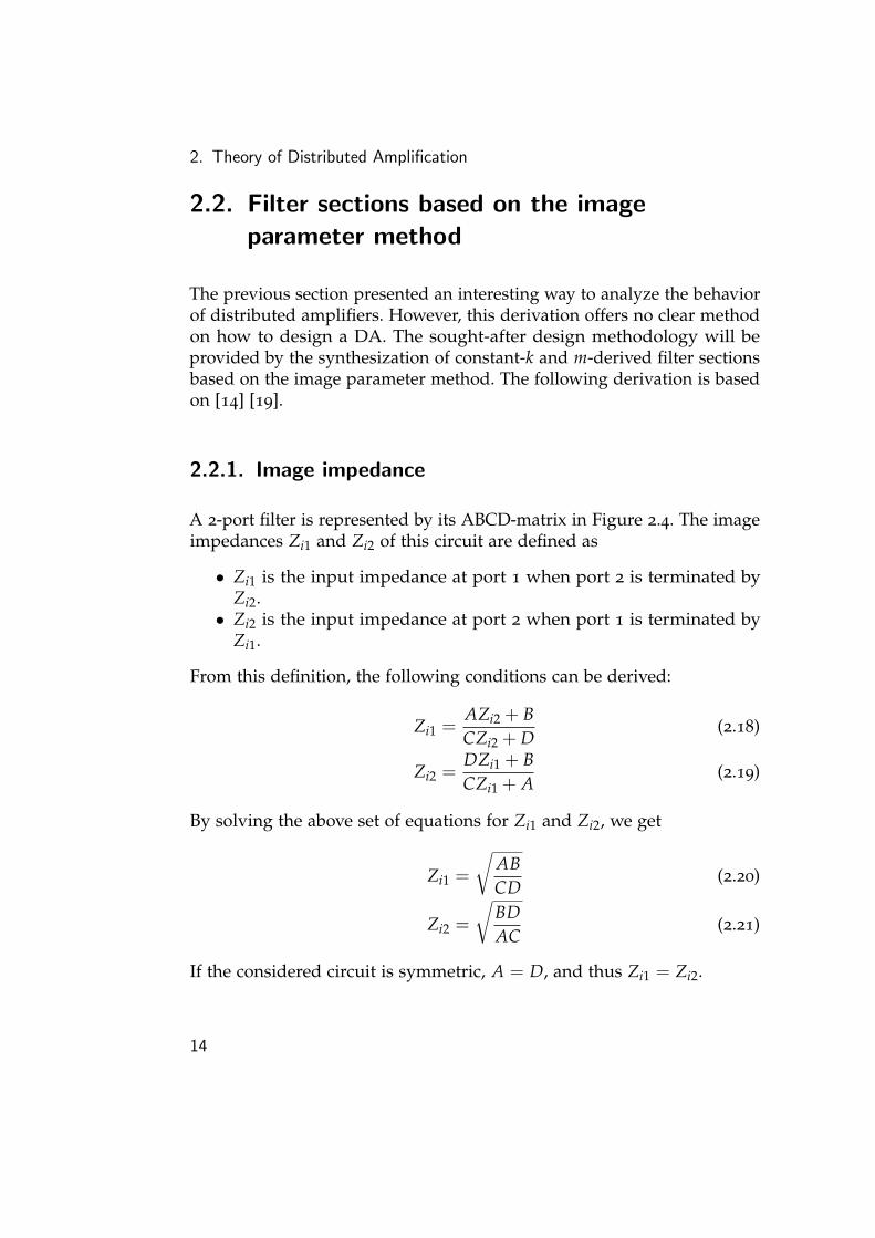
The previous section presented an interesting way to analyze the behaviorof distributed amplifiers. However, this derivation offers no clear methodon how to design a DA. The sought-after design methodology will beprovided by the synthesization of constant-k and m-derived filter sectionsbased on the image parameter method. The following derivation is basedon [14] [19].
2.2.1. Image impedance
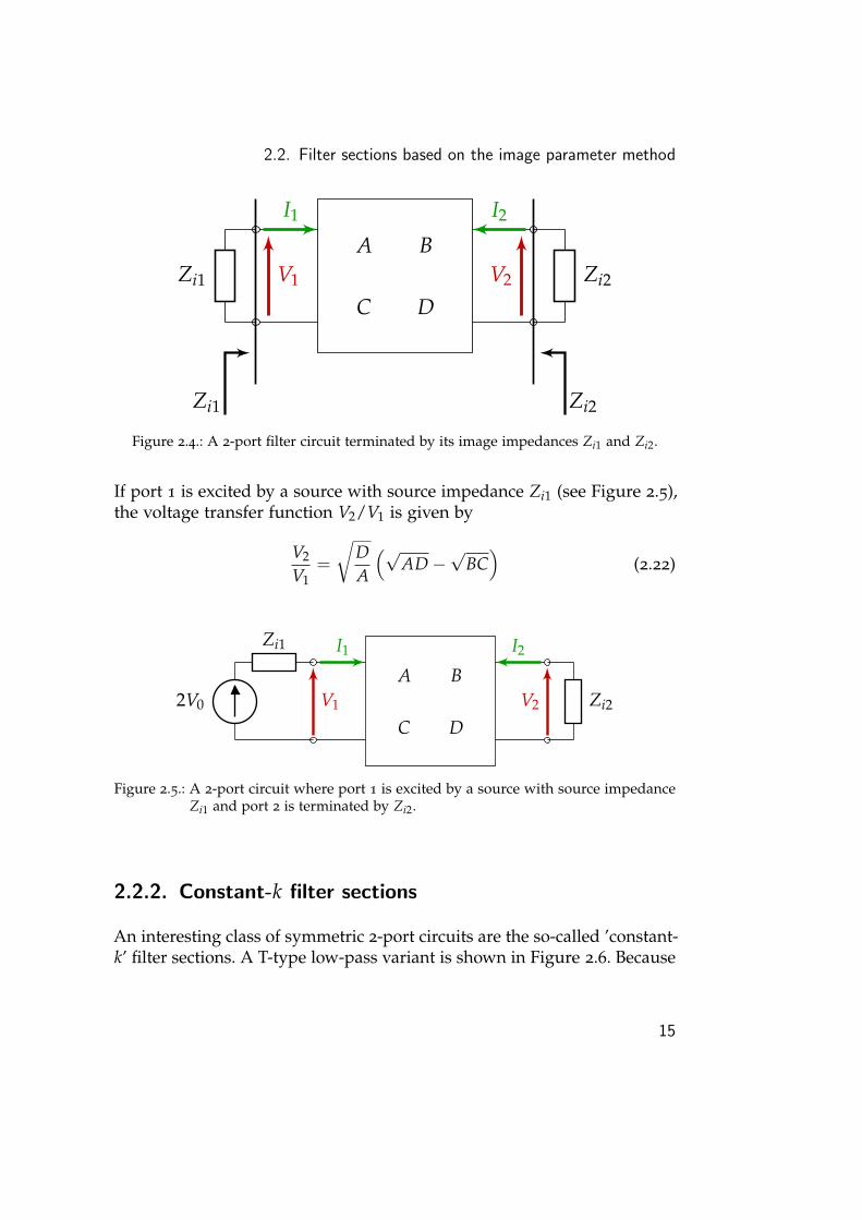
A 2-port filter is represented by its ABCD-matrix in Figure 2.4. The imageimpedances Zi1 and Zi2 of this circuit are defined as
• Zi1 is the input impedance at port 1 when port 2 is terminated byZi2.
• Zi2 is the input impedance at port 2 when port 1 is terminated byZi1.
From this definition, the following conditions can be derived:
Zi1 =AZi2 + BCZi2 + D
(2.18)
Zi2 =DZi1 + BCZi1 + A
(2.19)
By solving the above set of equations for Zi1 and Zi2, we get
Zi1 =
√ABCD
(2.20)
Zi2 =
√BDAC
(2.21)
If the considered circuit is symmetric, A = D, and thus Zi1 = Zi2.
14
2.2. Filter sections based on the image parameter method
A B
C DZi1 Zi2V1 V2
I1 I2
Zi1 Zi2
Figure 2.4.: A 2-port filter circuit terminated by its image impedances Zi1 and Zi2.
If port 1 is excited by a source with source impedance Zi1 (see Figure 2.5),the voltage transfer function V2/V1 is given by
V2
V1=
√DA
(√AD−
√BC)
(2.22)
A B
C D2V0
Zi1
Zi2V1 V2
I1 I2
Figure 2.5.: A 2-port circuit where port 1 is excited by a source with source impedanceZi1 and port 2 is terminated by Zi2.
2.2.2. Constant-k filter sections
An interesting class of symmetric 2-port circuits are the so-called ’constant-k’ filter sections. A T-type low-pass variant is shown in Figure 2.6. Because
15
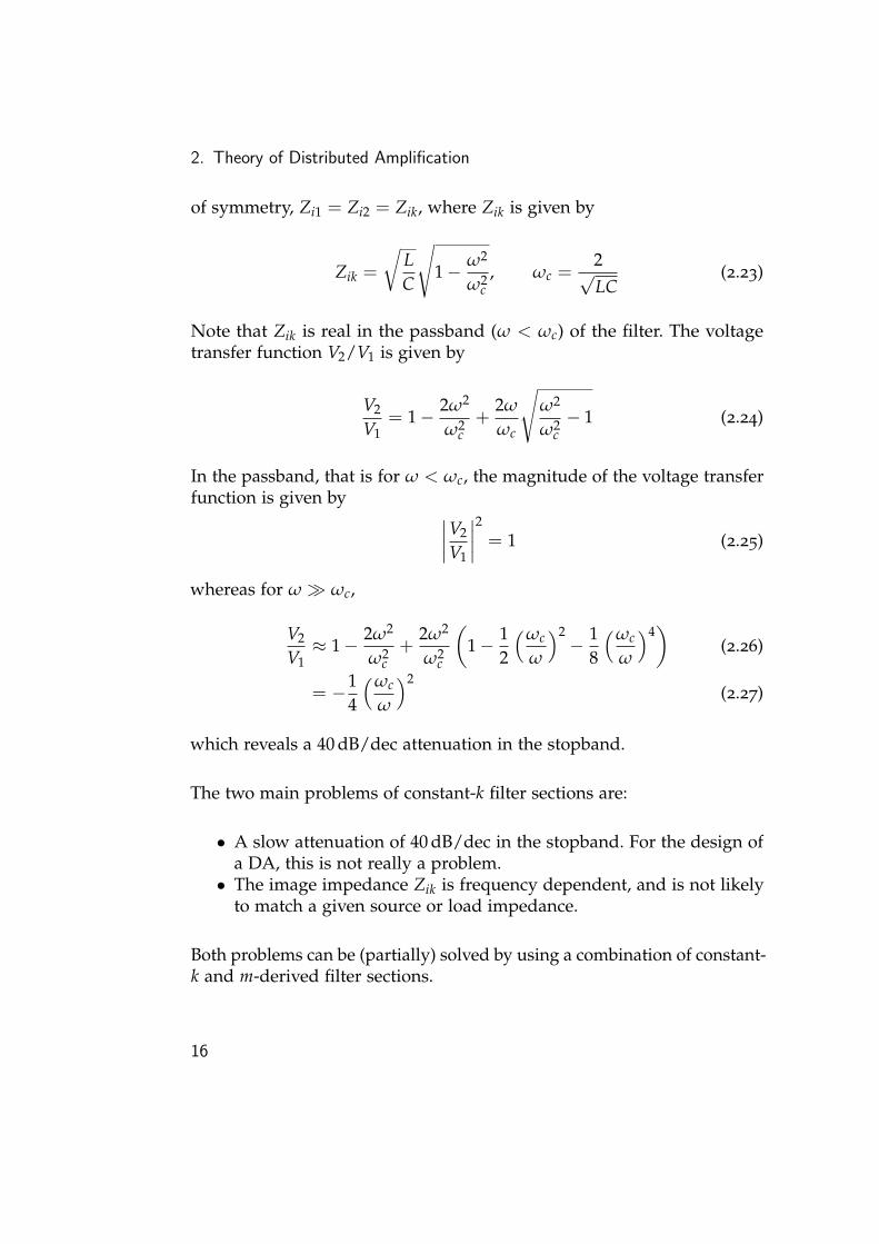
2. Theory of Distributed Amplification
of symmetry, Zi1 = Zi2 = Zik, where Zik is given by
Zik =
√LC
√1− ω2
ω2c
, ωc =2√LC
(2.23)
Note that Zik is real in the passband (ω < ωc) of the filter. The voltagetransfer function V2/V1 is given by
V2
V1= 1− 2ω2
ω2c+
2ω
ωc
√ω2
ω2c− 1 (2.24)
In the passband, that is for ω < ωc, the magnitude of the voltage transferfunction is given by
∣∣∣∣V2
V1
∣∣∣∣2
= 1 (2.25)
whereas for ω ωc,
V2
V1≈ 1− 2ω2
ω2c+
2ω2
ω2c
(1− 1
2
(ωc
ω
)2− 1
8
(ωc
ω
)4)
(2.26)
= −14
(ωc
ω
)2(2.27)
which reveals a 40 dB/dec attenuation in the stopband.
The two main problems of constant-k filter sections are:
• A slow attenuation of 40 dB/dec in the stopband. For the design ofa DA, this is not really a problem.• The image impedance Zik is frequency dependent, and is not likely
to match a given source or load impedance.
Both problems can be (partially) solved by using a combination of constant-k and m-derived filter sections.
16
2.2. Filter sections based on the image parameter method
L/2 L/2
C2V0
Zik
ZikV1 V2
I1 I2
Zik Zik
Figure 2.6.: A constant-k T-type low-pass filter section.
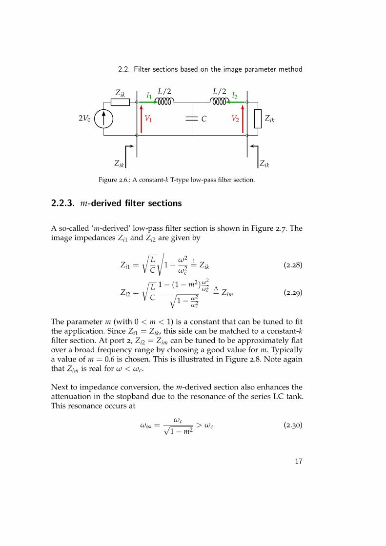
2.2.3. m-derived filter sections
A so-called ’m-derived’ low-pass filter section is shown in Figure 2.7. Theimage impedances Zi1 and Zi2 are given by
Zi1 =
√LC
√1− ω2
ω2c
!= Zik (2.28)
Zi2 =
√LC
1− (1−m2)ω2
ω2c√
1− ω2
ω2c
∆= Zim (2.29)
The parameter m (with 0 < m < 1) is a constant that can be tuned to fitthe application. Since Zi1 = Zik, this side can be matched to a constant-kfilter section. At port 2, Zi2 = Zim can be tuned to be approximately flatover a broad frequency range by choosing a good value for m. Typicallya value of m = 0.6 is chosen. This is illustrated in Figure 2.8. Note againthat Zim is real for ω < ωc.
Next to impedance conversion, the m-derived section also enhances theattenuation in the stopband due to the resonance of the series LC tank.This resonance occurs at
ω∞ =ωc√
1−m2> ωc (2.30)
17

2. Theory of Distributed Amplification
mL2
1−m2
2m L
mC2
Zi1 Zi2V1 V2
I1 I2
Zi1 = Zik Zi2 = Zim
Figure 2.7.: An m-derived filter section terminated by its image impedances Zi1 = Zikand Zi2 = Zim.
0 0.1 0.2 0.3 0.4 0.5 0.6 0.7 0.8 0.9 1
0
0.2
0.4
0.6
0.8
1
1.2
1.4
1.6
1.8
2
m = 0.1
m = 0.4
m = 0.6
m = 0.9
ωωc
Zim√L/C
Figure 2.8.: The image impedance Zim for various values of the parameter m.
18
2.2. Filter sections based on the image parameter method
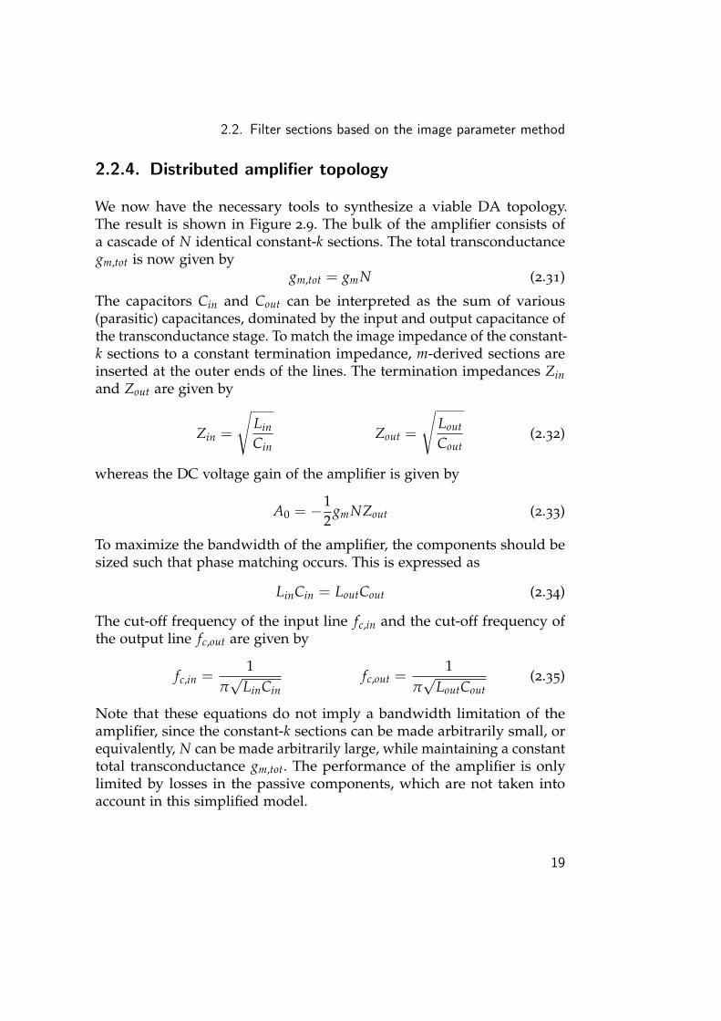
2.2.4. Distributed amplifier topology
We now have the necessary tools to synthesize a viable DA topology.The result is shown in Figure 2.9. The bulk of the amplifier consists ofa cascade of N identical constant-k sections. The total transconductancegm,tot is now given by
gm,tot = gmN (2.31)
The capacitors Cin and Cout can be interpreted as the sum of various(parasitic) capacitances, dominated by the input and output capacitance ofthe transconductance stage. To match the image impedance of the constant-k sections to a constant termination impedance, m-derived sections areinserted at the outer ends of the lines. The termination impedances Zinand Zout are given by
Zin =
√Lin
CinZout =
√Lout
Cout(2.32)
whereas the DC voltage gain of the amplifier is given by
A0 = −12
gmNZout (2.33)
To maximize the bandwidth of the amplifier, the components should besized such that phase matching occurs. This is expressed as
LinCin = LoutCout (2.34)
The cut-off frequency of the input line fc,in and the cut-off frequency ofthe output line fc,out are given by
fc,in =1
π√
LinCinfc,out =
1π√
LoutCout(2.35)
Note that these equations do not imply a bandwidth limitation of theamplifier, since the constant-k sections can be made arbitrarily small, orequivalently, N can be made arbitrarily large, while maintaining a constanttotal transconductance gm,tot. The performance of the amplifier is onlylimited by losses in the passive components, which are not taken intoaccount in this simplified model.
19

2. Theory of Distributed Amplification
mLin2
1−m2
2m Lin
mCin2
Lin2
Lin2
Cin
Lin2
Lin2
Cin
mLin2
1−m2
2m Lin
mCin2
X1 XN
source m-derived constant-k section 1 constant-k section N m-derived termination
mLout2
1−m2
2m Lout
mCout2
Lout2
Lout2
Cout gmX1
Lout2
Lout2
Cout gmXN
mLout2
1−m2
2m Lout
mCout2
Zout
2V0
Zin
Zout
Zin
termination m-derived constant-k section 1 constant-k section N m-derived load
Figure 2.9.: DA topology based on constant-k and m-derived filter sections.
Numerical example
The operation of the DA is illustrated by means of a numerical example.A set of well-chosen values is given in Table 2.1. The simulation results arepresented in Figure 2.10. As expected, the amplifier shows a gain of 20 dBover a very broad bandwidth. The m-derived sections guarantee excellentmatching over the entire frequency range. The peaking present in |S21|is in practice not a problem, since it will disappear due to losses in thepassive components. The group delay shows the same peaking behavioras |S21|.
Lin 250 pH Zin 50 ΩCin 100 fF Zout 50 ΩLout 250 pH fc,in 63.7 GHzCout 100 fF fc,out 63.7 GHzgm 100 mS A0 −10m 0.6 N 4
Table 2.1.: Numerical values for the components of the DA shown in Figure 2.9.
20

2.2. Filter sections based on the image parameter method
1.0 10.0 100.0
f [GHz]
-100
-80
-60
-40
-20
0
|S1
1| [d
B]
(a) S11
0.1 1.0 10.0 100.0
f [GHz]
0
10
20
30
40
|S2
1| [d
B]
(b) S21
0.1 1.0 10.0 100.0
f [GHz]
0.0
50.0
100.0
150.0
200.0
250.0
gro
up d
ela
y [ps]
(c) group delay
Figure 2.10.: Simulation results of the circuit shown in Figure 2.9 with the numericalvalues of Table 2.1.
21

3. Transconductance Stage
A distributed amplifier consists of the parallel interconnection of amplifierstages using inductors. In the case of an optical modulator driver, thesestages should be broadband and resistant to high voltage swings. Thischapter discusses the transconductance stages which will later be used inChapter 5 to build a distributed amplifier.
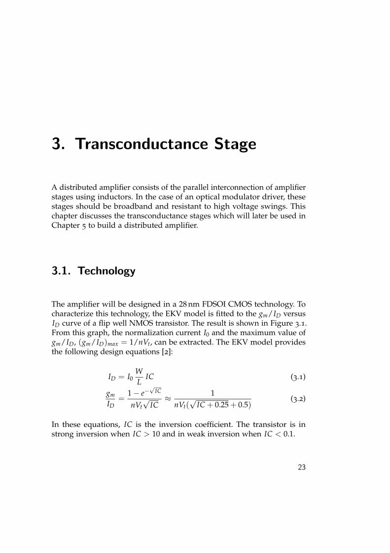
3.1. Technology
The amplifier will be designed in a 28 nm FDSOI CMOS technology. Tocharacterize this technology, the EKV model is fitted to the gm/ID versusID curve of a flip well NMOS transistor. The result is shown in Figure 3.1.From this graph, the normalization current I0 and the maximum value ofgm/ID, (gm/ID)max = 1/nVt, can be extracted. The EKV model providesthe following design equations [2]:
ID = I0WL
IC (3.1)
gm
ID=
1− e−√
IC
nVt√
IC≈ 1
nVt(√
IC + 0.25 + 0.5)(3.2)
In these equations, IC is the inversion coefficient. The transistor is instrong inversion when IC > 10 and in weak inversion when IC < 0.1.
23

3. Transconductance Stage
Cadence simulation
EKV model
approximate EKV model
gmID
nVt
IDW/L
I0
2
10.8
0.6
0.4
0.2
0.1
Figure 3.1.: EKV model of a flip well NMOS transistor in the available technology.
3.2. Modified cascode circuit
To build a DA, a transconductance stage is required which meets thefollowing requirements:
• A high output resistance: the finite output resistance of the transcon-ductance stage acts as a loss resistance on the output TL. Increasingthe output resistance will decrease losses.• Resistant to large output voltages: the amplifier should produce an
output voltage swing of 2 VPP. Since the transistors of the sub-microntechnology cannot withstand such high voltages, this large swingshould be distributed over multiple transistors.• Highly unilateral: if the transconductance stage would not be uni-
lateral, signals excited on the output TL can couple back into theinput TL, altering the behavior of the amplifier. A high isolation alsoensures that the input capacitance of the stage Cts
in is independent ofthe load impedance (the output TL), and that the output capacitanceCts
out is independent of the source impedance (the input TL). Thissimplifies the design of the DA.
24
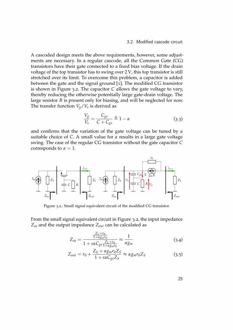
3.2. Modified cascode circuit
A cascoded design meets the above requirements, however, some adjust-ments are necessary. In a regular cascode, all the Common Gate (CG)transistors have their gate connected to a fixed bias voltage. If the drainvoltage of the top transistor has to swing over 2 V, this top transistor is stillstretched over its limit. To overcome this problem, a capacitor is addedbetween the gate and the signal ground [1]. The modified CG transistoris shown in Figure 3.2. The capacitor C allows the gate voltage to vary,thereby reducing the otherwise potentially large gate-drain voltage. Thelarge resistor R is present only for biasing, and will be neglected for now.The transfer function Vg/Vs is derived as
Vg
Vs=
Cgs
C + Cgs, 1− α (3.3)
and confirms that the variation of the gate voltage can be tuned by asuitable choice of C. A small value for α results in a large gate voltageswing. The case of the regular CG transistor without the gate capacitor Ccorresponds to α = 1.
C RZS ZL
Iin
Iout
Zin Zout
r0
Cgs
C R
gmXX
ZS ZLIin
Iout
Zin Zout
VsVg
Figure 3.2.: Small signal equivalent circuit of the modified CG transistor.
From the small signal equivalent circuit in Figure 3.2, the input impedanceZin and the output impedance Zout can be calculated as
Zin =
ZL+r01+αgmr0
1 + sαCgsZL+r0
1+αgmr0
≈ 1αgm
(3.4)
Zout = r0 +ZS + αgmr0ZS
1 + sαCgsZS≈ αgmr0ZS (3.5)
25
3. Transconductance Stage
where α = CC+Cgs
. In the above low frequency approximations, the designequations of a regular CG transistor can be recognized, however, nowa factor α has been introduced. The modified CG transistor is furthercharacterized by its short circuit current Isc. For ZL = 0, we get
Iout = Isc =
1+αgmr0
1+ r0ZS
+αgmr0
1 + s r0αCgs
1+ r0ZS
+αgmr0
Iin ≈1 + αgmr0
1 + r0ZS
+ αgmr0Iin (3.6)
From (3.4)-(3.6) we observe the following:
• Since α < 1, Zin will increase and Zout will decrease w.r.t. the case ofα = 1. This is not beneficial for the correct cascode behavior, whichrequires that the input impedance of every CG transistor is muchsmaller than the output impedance of the preceding CG transistor.• In the case where gmr0 is not very large (this is a valid concern in
contemporary CMOS technologies) and ZS is of the same order ofmagnitude as r0 (for example if the CG transistor is preceded by aCS transistor), Isc will deviate from Iin.
The above concerns are only valid if ZS is not large enough. To havemaximum freedom in tuning α, it may be recommended to use at least oneregular CG transistor after the CS transistor. This is shown in Figure 3.3.
3.2.1. Biasing
To bias the modified CG transistor, a large resistor R is inserted betweenthe gate of the transistor and a suitable bias voltage. The complete Vg/Vstransfer function (see Figure 3.2) is given by
Vg
Vs=
sRCgs
1 + sR(C + Cgs)(3.7)
The gate voltage swing drops to zero at low frequencies, resulting in thepotential breakdown of the transistor. To prevent this, signals with largefrequency components below fmin = 1
2πR(C+Cgs)should not be applied to
26

3.2. Modified cascode circuit
the amplifier. In practice this comes down to avoiding long periods ofconsecutive ’0’ bits or ’1’ bits. The resistor R should be sized as large aspossible to keep the minimum operating frequency fmin as low as possible.The complete circuit of the cascode is presented in Figure 3.3. The exactsizing of the resistors R3 and R4 will be discussed in Chapter 5.
C3
C4
M1
M2
M3
M4
R3
R4
Vg3
Vg4
Vg2
in
out
Figure 3.3.: Triple cascode with an additional gate capacitor at the top two CG transistors.These top two transistors are biased via the large resistors R3 and R4.
3.2.2. Transistor and capacitor sizing
To size the CS transistor M1, the value of gm is calculated from
A0 = −12
gmNZout (3.8)
The number of transconductance stages N is an important parameter in thedesign of a DA, and will be discussed in Chapter 5. For N = 6, A0 = −10
27
3. Transconductance Stage
and Zout = 50 Ω, we get gm = 66.6 mS. The CS transistor M1 should bebiased in strong inversion (IC > 10) to ensure the linear operation ofthe amplifier, and as such requires a large drain current ID. However, Inpractice this current has to flow through the inductors of the output TL ofthe DA. Even when the width of these inductor traces is maximized, thecurrent is limited to ID = 10 mA per transconductance stage (see Chapter4). Given that gm = 66.6 mS, we get gm/ID = 6.66 V−1, which results via(3.2) in a value of IC slightly smaller than 10. From ID = 10 mA and IC,the width W1 of M1 can now be calculated using (3.1), assuming minimallength.
A number of strategies exist on the sizing of the CG transistors M2, M3and M4. As described in [13], one could try to size the capacitors C3 andC4 and the transistors M2, M3 and M4 to obtain an equal drain-sourcevoltage swing over all transistors. Nevertheless, this approach requiresrather large values of gmi, resulting in a large output capacitance Cts
outof the transconductance stage. A large output capacitance will require
large inductors (via Zout =√
LoutCout
= 50 Ω) which have more parasitics (seeChapter 4), eventually degrading the performance of the DA.A second approach would consist of minimizing the size of the CG transis-tors, thereby minimizing Cts
out, while still maintaining sufficient flexibilityin tuning the voltage swing over all transistors using C3 and C4. Due totime constraints, this path was not further explored.A last strategy consists of sizing all CG transistors equal to the CS transis-tor M1: W1 = W2 = W3 = W4. It turns out that, by tuning only C3 and C4and the bias voltages Vg2, Vg3 and Vg4, the output voltage swing can besufficiently distributed over the individual transistors of the cascode, whilekeeping the output capacitance of the cascode Cts
out adequately low. Theexact sizing of the capacitors and the bias voltages can only be determinedwhen the entire distributed amplifier is considered, and as a consequencethis is further discussed in Chapter 5.
28
3.3. Series peaking
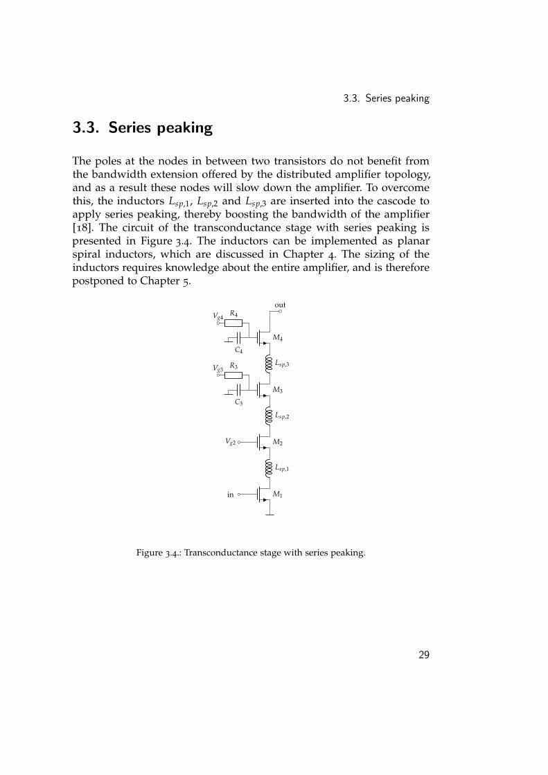
3.3. Series peaking
The poles at the nodes in between two transistors do not benefit fromthe bandwidth extension offered by the distributed amplifier topology,and as a result these nodes will slow down the amplifier. To overcomethis, the inductors Lsp,1, Lsp,2 and Lsp,3 are inserted into the cascode toapply series peaking, thereby boosting the bandwidth of the amplifier[18]. The circuit of the transconductance stage with series peaking ispresented in Figure 3.4. The inductors can be implemented as planarspiral inductors, which are discussed in Chapter 4. The sizing of theinductors requires knowledge about the entire amplifier, and is thereforepostponed to Chapter 5.
Lsp,1
Lsp,2
Lsp,3
C3
C4
M1
M2
M3
M4
R3
R4
Vg3
Vg4
Vg2
in
out
Figure 3.4.: Transconductance stage with series peaking.
29

4. Inductors
This chapter discusses the design of on-chip inductors for use in a DA. Theperformance of a distributed amplifier is limited by the finite quality ofthe on-chip inductors, and these are therefore of utmost importance to thedesign. Since the constant-k series inductors are the most critical passivecomponents of the circuit, the largest part of this chapter is devoted tothem. Nevertheless, also the series peaking inductors in the transconduc-tance stages (see Figure 3.4) will be handled. The first three sections willdiscuss inductors on a more theoretical level. This theoretical insight willbe used in the last two sections to design high performance inductors.
4.1. Microstrip as inductor
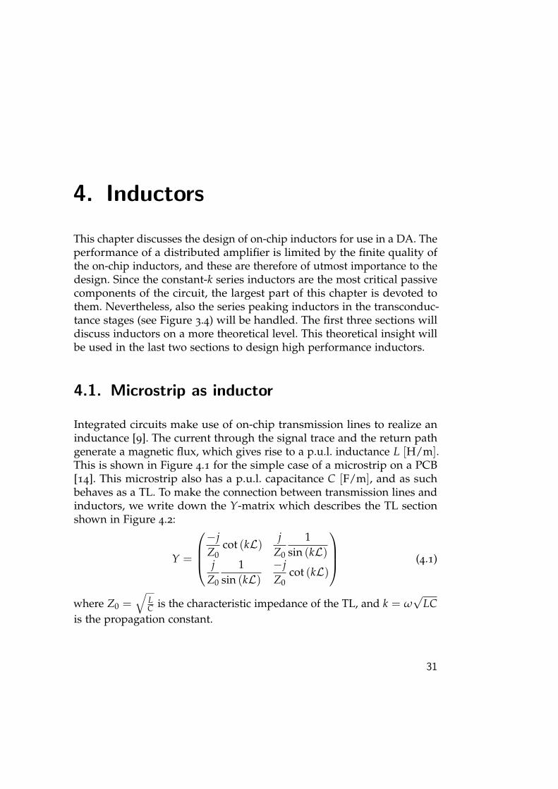
Integrated circuits make use of on-chip transmission lines to realize aninductance [9]. The current through the signal trace and the return pathgenerate a magnetic flux, which gives rise to a p.u.l. inductance L [H/m].This is shown in Figure 4.1 for the simple case of a microstrip on a PCB[14]. This microstrip also has a p.u.l. capacitance C [F/m], and as suchbehaves as a TL. To make the connection between transmission lines andinductors, we write down the Y-matrix which describes the TL sectionshown in Figure 4.2:
Y =
−jZ0
cot (kL) jZ0
1sin (kL)
jZ0
1sin (kL)
−jZ0
cot (kL)
(4.1)
where Z0 =√
LC is the characteristic impedance of the TL, and k = ω
√LC
is the propagation constant.
31
4. Inductors
I
I
ε, µ0
H
Figure 4.1.: Magnetic field lines of a microstrip on a PCB.
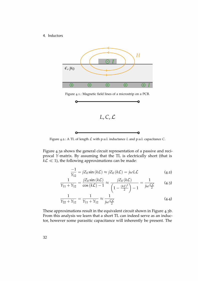
L, C,L
Figure 4.2.: A TL of length L with p.u.l. inductance L and p.u.l. capacitance C.
Figure 4.3a shows the general circuit representation of a passive and reci-procal Y-matrix. By assuming that the TL is electrically short (that iskL 1), the following approximations can be made:
−1Y12
= jZ0 sin (kL) ≈ jZ0 (kL) = jωLL (4.2)
1Y11 + Y12
=jZ0 sin (kL)cos (kL)− 1
≈ jZ0 (kL)(1− (kL)2
2
)− 1
=1
jω CL2
(4.3)
1Y22 + Y12
=1
Y11 + Y12≈ 1
jω CL2
(4.4)
These approximations result in the equivalent circuit shown in Figure 4.3b.From this analysis we learn that a short TL can indeed serve as an induc-tor, however some parasitic capacitance will inherently be present. The
32
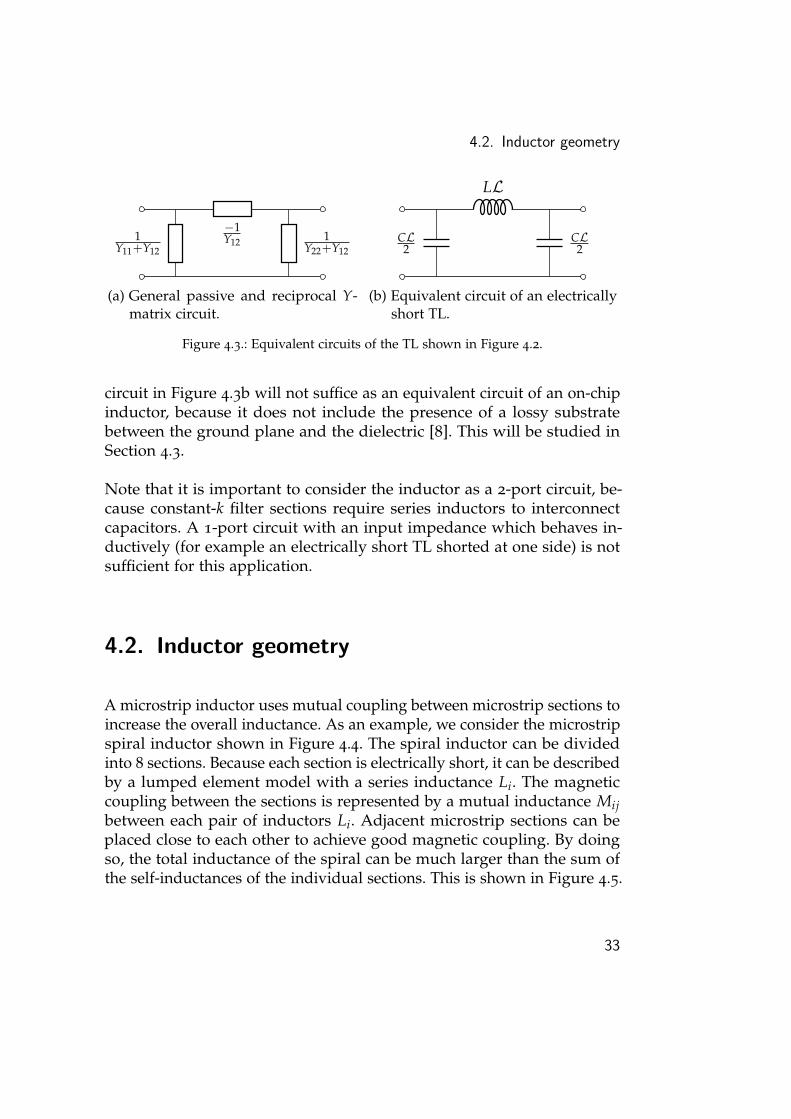
4.2. Inductor geometry
−1Y121
Y11+Y121
Y22+Y12
(a) General passive and reciprocal Y-matrix circuit.
LL
CL2
CL2
(b) Equivalent circuit of an electricallyshort TL.
Figure 4.3.: Equivalent circuits of the TL shown in Figure 4.2.
circuit in Figure 4.3b will not suffice as an equivalent circuit of an on-chipinductor, because it does not include the presence of a lossy substratebetween the ground plane and the dielectric [8]. This will be studied inSection 4.3.
Note that it is important to consider the inductor as a 2-port circuit, be-cause constant-k filter sections require series inductors to interconnectcapacitors. A 1-port circuit with an input impedance which behaves in-ductively (for example an electrically short TL shorted at one side) is notsufficient for this application.
4.2. Inductor geometry
A microstrip inductor uses mutual coupling between microstrip sections toincrease the overall inductance. As an example, we consider the microstripspiral inductor shown in Figure 4.4. The spiral inductor can be dividedinto 8 sections. Because each section is electrically short, it can be describedby a lumped element model with a series inductance Li. The magneticcoupling between the sections is represented by a mutual inductance Mijbetween each pair of inductors Li. Adjacent microstrip sections can beplaced close to each other to achieve good magnetic coupling. By doingso, the total inductance of the spiral can be much larger than the sum ofthe self-inductances of the individual sections. This is shown in Figure 4.5.
33
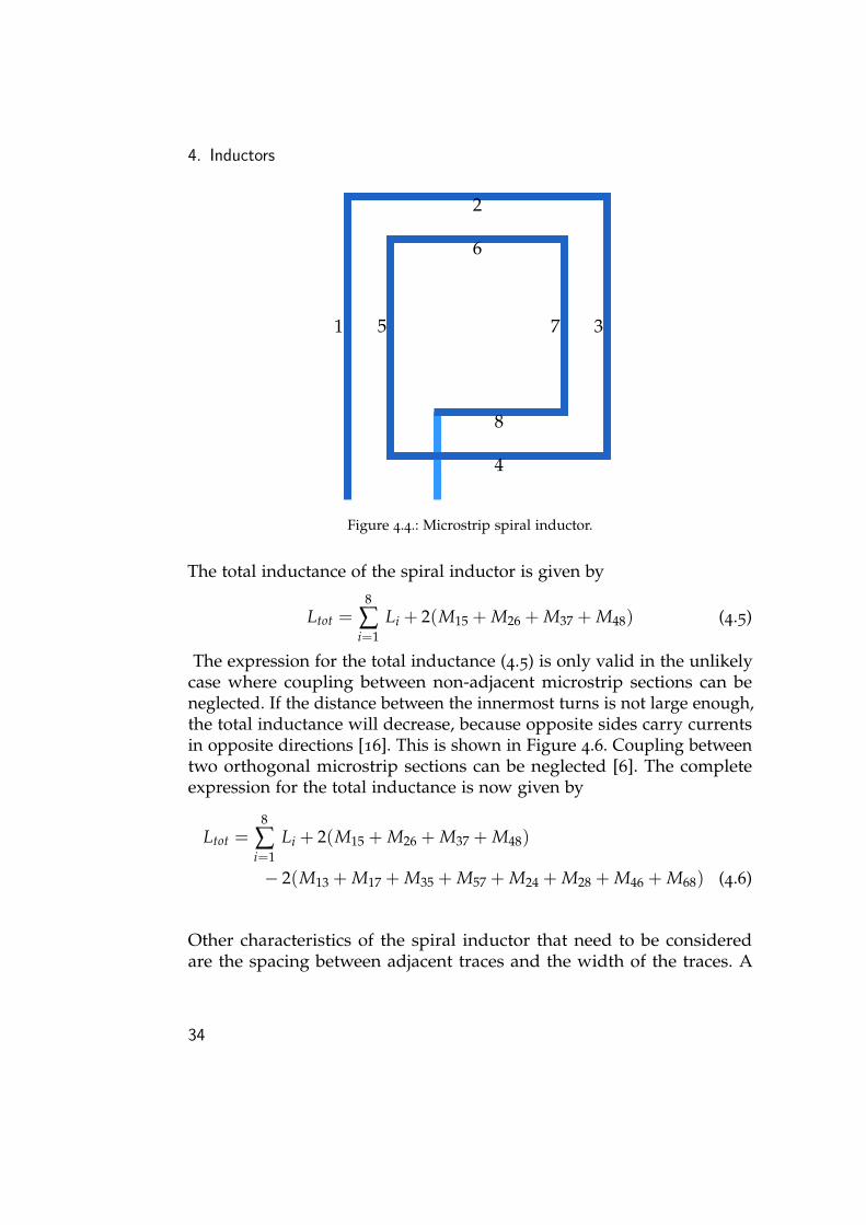
4. Inductors
1 5 7 3
2
6
4
8
Figure 4.4.: Microstrip spiral inductor.
The total inductance of the spiral inductor is given by
Ltot =8
∑i=1
Li + 2(M15 + M26 + M37 + M48) (4.5)
The expression for the total inductance (4.5) is only valid in the unlikelycase where coupling between non-adjacent microstrip sections can beneglected. If the distance between the innermost turns is not large enough,the total inductance will decrease, because opposite sides carry currentsin opposite directions [16]. This is shown in Figure 4.6. Coupling betweentwo orthogonal microstrip sections can be neglected [6]. The completeexpression for the total inductance is now given by
Ltot =8
∑i=1
Li + 2(M15 + M26 + M37 + M48)
− 2(M13 + M17 + M35 + M57 + M24 + M28 + M46 + M68) (4.6)
Other characteristics of the spiral inductor that need to be consideredare the spacing between adjacent traces and the width of the traces. A
34

4.2. Inductor geometry
L1
L2
L3
L4
L5
L6
L7
L8
M15 M37
M26
M48
Figure 4.5.: Microstrip spiral inductor equivalent circuit. Adjacent microstrip sections aretightly coupled.
small spacing between adjacent traces will allow for a tight couplingof magnetic fields, increasing the overall inductance. This will, however,also increase the parasitic capacitance between the windings of the spiral,lowering the self-resonance frequency (SRF) of the inductor. By increasingthe width of the traces, the series resistance of the lines will decrease,but the capacitance between the signal trace and the ground plane willincrease. In the case of an on-chip microstrip inductor, wider traces havea higher capacitive coupling to the substrate, leading to higher substratelosses.
35

4. Inductors
L1
L2
L3
L4
L5
L6
L7
L8
M57
M35
M17
M13
L1
L2
L3
L4
L5
L6
L7
L8
M68
M46
M28
M24
Figure 4.6.: Reduction of the total inductance due to coupling between opposite sides ofthe spiral carrying opposite currents.
4.3. Equivalent circuit of an on-chip microstripinductor
We now consider on-chip microstrip inductors. The performance of a DAis limited by the losses in the inductors. These losses are mainly attributedto the series resistance of the microstrip lines and the finite resistivityof the substrate. To get more insight into the effect of these losses onthe performance of a DA, we construct an equivalent circuit of an on-chip microstrip inductor. A typical lumped model of the semiconductorsubstrate and the dielectric is shown in Figure 4.7 [8].
We have now gathered the necessary insight to construct a heavily sim-plified equivalent circuit of an on-chip microstrip inductor. The result isshown in Figure 4.8 [16]. In this circuit, Rsub, Csub and Cdi are as explainedin Figure 4.7. The total inductance (see (4.6)) of the inductor is representedby L, whereas the total series resistance of the microstrip lines is repre-sented by RS. The interwinding capacitance is modelled by CF, which willdetermine the SRF of the inductor.
36
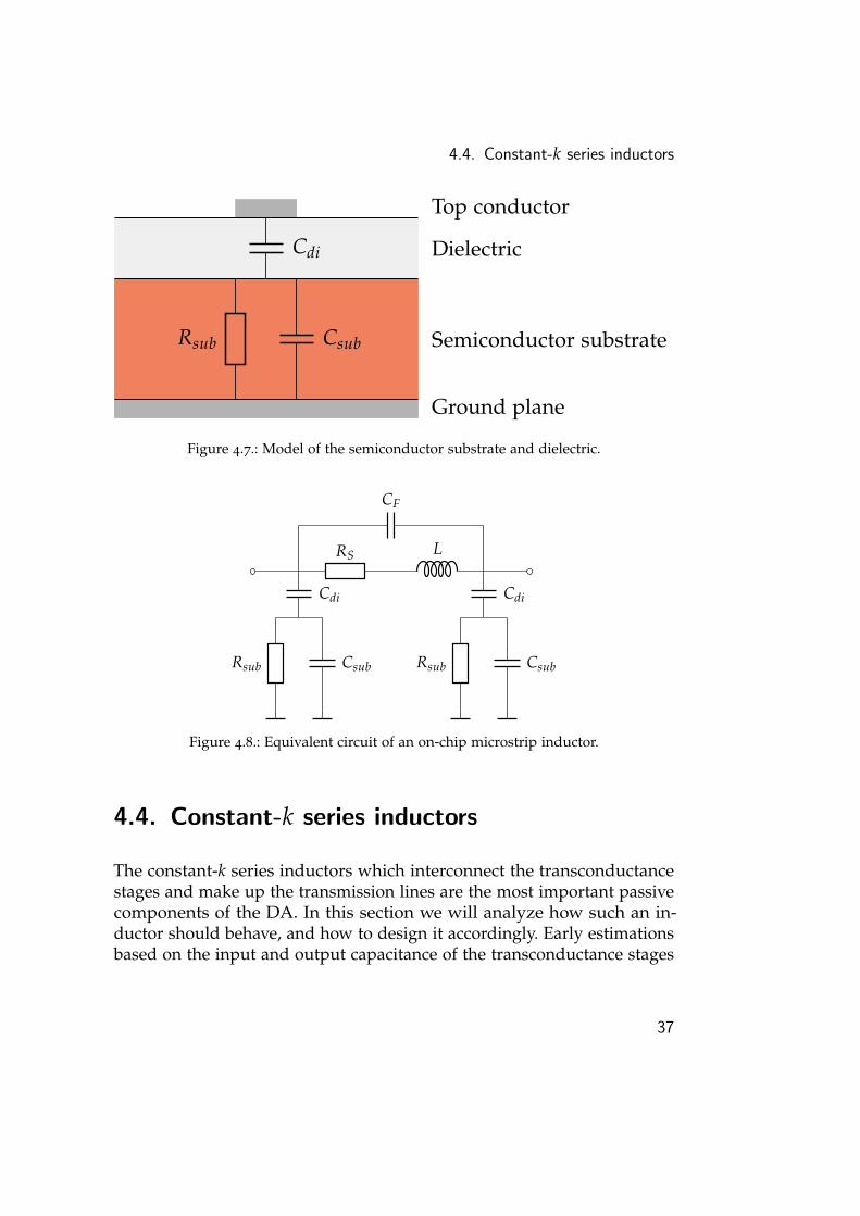
4.4. Constant-k series inductors
Cdi
Rsub Csub
Top conductor
Dielectric
Semiconductor substrate
Ground plane
Figure 4.7.: Model of the semiconductor substrate and dielectric.
RS L
CF
Cdi
Rsub Csub
Cdi
Rsub Csub
Figure 4.8.: Equivalent circuit of an on-chip microstrip inductor.
4.4. Constant-k series inductors
The constant-k series inductors which interconnect the transconductancestages and make up the transmission lines are the most important passivecomponents of the DA. In this section we will analyze how such an in-ductor should behave, and how to design it accordingly. Early estimationsbased on the input and output capacitance of the transconductance stages
37
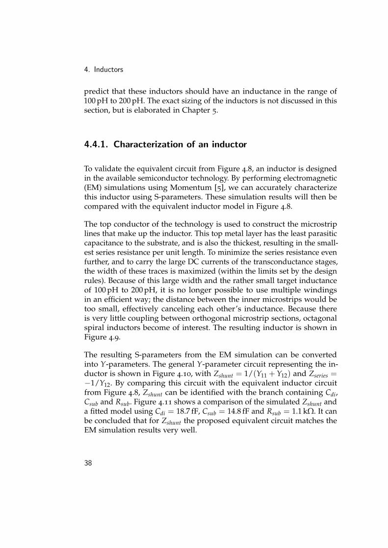
4. Inductors
predict that these inductors should have an inductance in the range of100 pH to 200 pH. The exact sizing of the inductors is not discussed in thissection, but is elaborated in Chapter 5.
4.4.1. Characterization of an inductor
To validate the equivalent circuit from Figure 4.8, an inductor is designedin the available semiconductor technology. By performing electromagnetic(EM) simulations using Momentum [5], we can accurately characterizethis inductor using S-parameters. These simulation results will then becompared with the equivalent inductor model in Figure 4.8.
The top conductor of the technology is used to construct the microstriplines that make up the inductor. This top metal layer has the least parasiticcapacitance to the substrate, and is also the thickest, resulting in the small-est series resistance per unit length. To minimize the series resistance evenfurther, and to carry the large DC currents of the transconductance stages,the width of these traces is maximized (within the limits set by the designrules). Because of this large width and the rather small target inductanceof 100 pH to 200 pH, it is no longer possible to use multiple windingsin an efficient way; the distance between the inner microstrips would betoo small, effectively canceling each other’s inductance. Because thereis very little coupling between orthogonal microstrip sections, octagonalspiral inductors become of interest. The resulting inductor is shown inFigure 4.9.
The resulting S-parameters from the EM simulation can be convertedinto Y-parameters. The general Y-parameter circuit representing the in-ductor is shown in Figure 4.10, with Zshunt = 1/(Y11 + Y12) and Zseries =−1/Y12. By comparing this circuit with the equivalent inductor circuitfrom Figure 4.8, Zshunt can be identified with the branch containing Cdi,Csub and Rsub. Figure 4.11 shows a comparison of the simulated Zshunt anda fitted model using Cdi = 18.7 fF, Csub = 14.8 fF and Rsub = 1.1 kΩ. It canbe concluded that for Zshunt the proposed equivalent circuit matches theEM simulation results very well.
38
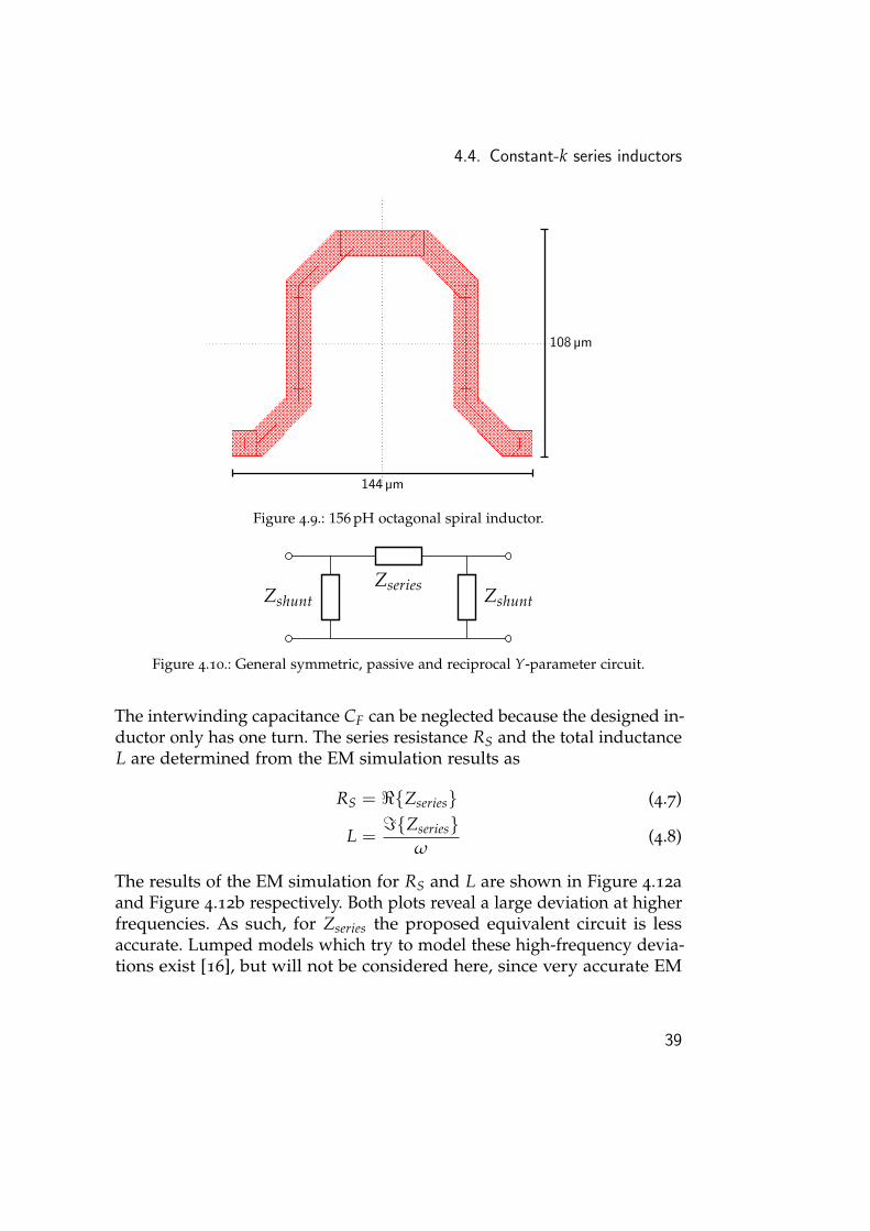
4.4. Constant-k series inductors
144 µm
108 µm
Figure 4.9.: 156 pH octagonal spiral inductor.
ZseriesZshunt Zshunt
Figure 4.10.: General symmetric, passive and reciprocal Y-parameter circuit.
The interwinding capacitance CF can be neglected because the designed in-ductor only has one turn. The series resistance RS and the total inductanceL are determined from the EM simulation results as
RS = <Zseries (4.7)
L ==Zseries
ω(4.8)
The results of the EM simulation for RS and L are shown in Figure 4.12aand Figure 4.12b respectively. Both plots reveal a large deviation at higherfrequencies. As such, for Zseries the proposed equivalent circuit is lessaccurate. Lumped models which try to model these high-frequency devia-tions exist [16], but will not be considered here, since very accurate EM
39
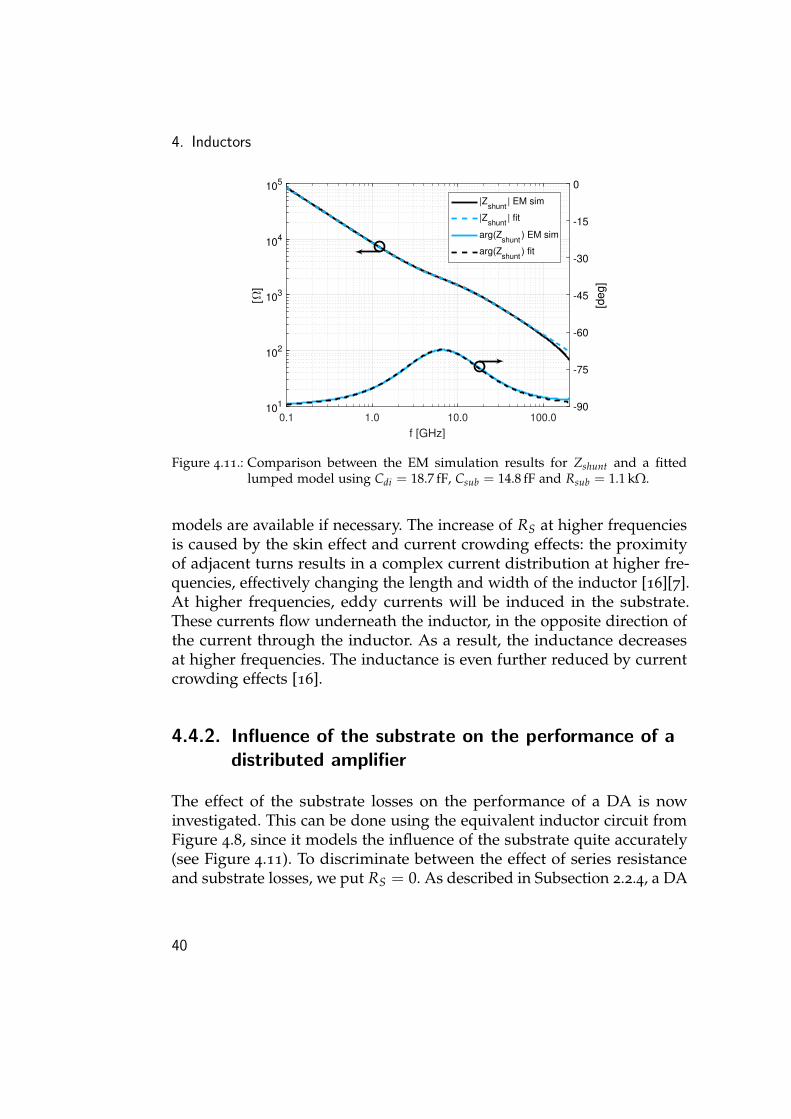
4. Inductors
0.1 1.0 10.0 100.0
f [GHz]
101
102
103
104
105
[]
-90
-75
-60
-45
-30
-15
0
[de
g]
|Zshunt
| EM sim
|Zshunt
| fit
arg(Zshunt
) EM sim
arg(Zshunt
) fit
Figure 4.11.: Comparison between the EM simulation results for Zshunt and a fittedlumped model using Cdi = 18.7 fF, Csub = 14.8 fF and Rsub = 1.1 kΩ.
models are available if necessary. The increase of RS at higher frequenciesis caused by the skin effect and current crowding effects: the proximityof adjacent turns results in a complex current distribution at higher fre-quencies, effectively changing the length and width of the inductor [16][7].At higher frequencies, eddy currents will be induced in the substrate.These currents flow underneath the inductor, in the opposite direction ofthe current through the inductor. As a result, the inductance decreasesat higher frequencies. The inductance is even further reduced by currentcrowding effects [16].
4.4.2. Influence of the substrate on the performance of adistributed amplifier
The effect of the substrate losses on the performance of a DA is nowinvestigated. This can be done using the equivalent inductor circuit fromFigure 4.8, since it models the influence of the substrate quite accurately(see Figure 4.11). To discriminate between the effect of series resistanceand substrate losses, we put RS = 0. As described in Subsection 2.2.4, a DA
40
4.4. Constant-k series inductors
0.1 1.0 10.0 100.0
f [GHz]
-3
-2
-1
0
1
2
RS [
]
(a) Simulated series resistance RS.
0.1 1.0 10.0 100.0
f [GHz]
60.0
80.0
100.0
120.0
140.0
160.0
L [
pH
]
(b) Simulated inductance L.
Figure 4.12.: Simulation results of the series resistance RS and the inductance L.
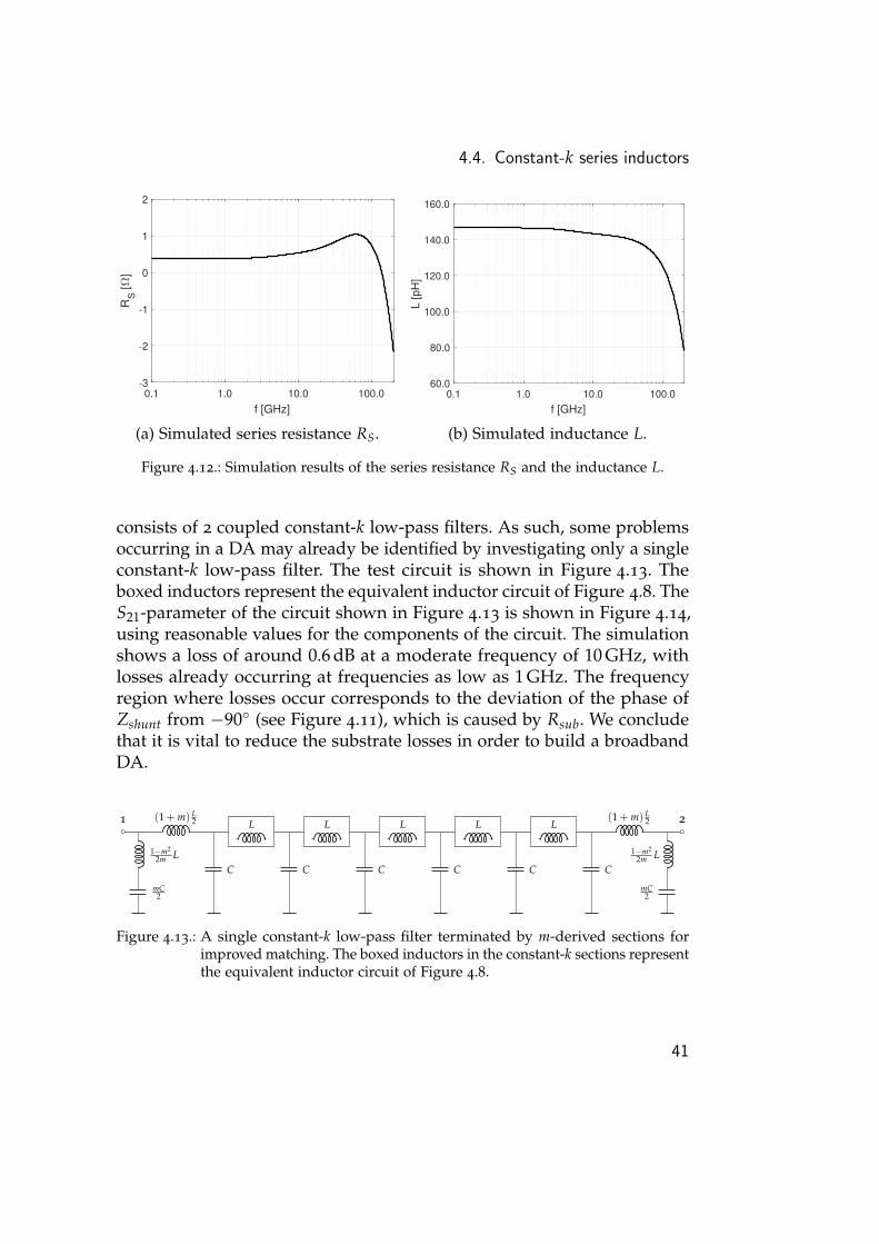
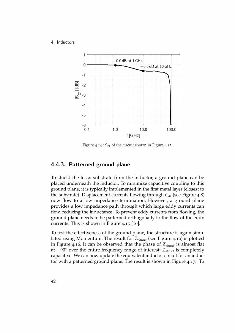
consists of 2 coupled constant-k low-pass filters. As such, some problemsoccurring in a DA may already be identified by investigating only a singleconstant-k low-pass filter. The test circuit is shown in Figure 4.13. Theboxed inductors represent the equivalent inductor circuit of Figure 4.8. TheS21-parameter of the circuit shown in Figure 4.13 is shown in Figure 4.14,using reasonable values for the components of the circuit. The simulationshows a loss of around 0.6 dB at a moderate frequency of 10 GHz, withlosses already occurring at frequencies as low as 1 GHz. The frequencyregion where losses occur corresponds to the deviation of the phase ofZshunt from −90 (see Figure 4.11), which is caused by Rsub. We concludethat it is vital to reduce the substrate losses in order to build a broadbandDA.
(1 + m) L2
1−m2
2m L
mC2
L L L L L
C C C C C C
(1 + m) L2
1−m2
2m L
mC2
1 2
Figure 4.13.: A single constant-k low-pass filter terminated by m-derived sections forimproved matching. The boxed inductors in the constant-k sections representthe equivalent inductor circuit of Figure 4.8.
41
4. Inductors
0.1 1.0 10.0 100.0
f [GHz]
-6
-5
-4
-3
-2
-1
0
1
|S2
1| [d
B]
−0.0 dB at 1GHz−0.6 dB at 10GHz
Figure 4.14.: S21 of the circuit shown in Figure 4.13.
4.4.3. Patterned ground plane
To shield the lossy substrate from the inductor, a ground plane can beplaced underneath the inductor. To minimize capacitive coupling to thisground plane, it is typically implemented in the first metal layer (closest tothe substrate). Displacement currents flowing through Cdi (see Figure 4.8)now flow to a low impedance termination. However, a ground planeprovides a low impedance path through which large eddy currents canflow, reducing the inductance. To prevent eddy currents from flowing, theground plane needs to be patterned orthogonally to the flow of the eddycurrents. This is shown in Figure 4.15 [16].
To test the effectiveness of the ground plane, the structure is again simu-lated using Momentum. The result for Zshunt (see Figure 4.10) is plottedin Figure 4.16. It can be observed that the phase of Zshunt is almost flatat −90 over the entire frequency range of interest: Zshunt is completelycapacitive. We can now update the equivalent inductor circuit for an induc-tor with a patterned ground plane. The result is shown in Figure 4.17. To
42

4.4. Constant-k series inductors
Figure 4.15.: Patterned ground plane under the inductor. The current in the ground planecannot flow in loops.
investigate the effect of the parasitic capacitance CL (see Figure 4.17), werevisit the constant-k filter of Figure 4.13, which is reprinted in Figure 4.18.The boxed inductors in the constant-k sections represent the equivalentinductor circuit of Figure 4.17. It can be observed that CL is in parallel toC0, and as such can be elegantly taken into account. By defining
C , C0 + 2CL (4.9)
we can use all the equations of Section 2.2 without altering the notations.Care must be taken at the boundaries of the filter, however, because thecapacitors C1 are only adjacent to one non-ideal inductor (in practice theinductors of the m-derived sections will be sized differently, and thus willhave a different parasitic capacitance than the inductors of the constant-ksections). In order that all nodes still have a total capacitance C, C1 shouldbe sized as C1 = C0 + CL.
The only remaining parasitic that still needs to be investigated is the seriesresistance RS. Since capacitive coupling to the substrate is no longer anissue, the microstrip traces can be made as wide as possible to reduceRS. Figure 4.19 shows a simulation of the S21-parameter of the circuit in
43

4. Inductors
0.1 1.0 10.0 100.0
f [GHz]
100
101
102
103
104
105
|Z
shunt|
[]
-90
-75
-60
-45
-30
-15
0
arg
(Zshunt)
[de
g]
Figure 4.16.: Zshunt of the inductor with a patterned ground plane.
RS L
CL CL
Figure 4.17.: Equivalent circuit of an inductor with a patterned ground plane.
Figure 4.18, using reasonable values for all the components and RS =0.5 Ω. The parasitic capacitance CL of the inductors was taken into accountas described above. The performance of the filter has much improvedsince the introduction of the patterned ground plane. The remaining loss(around 0.2 dB) appears to be constant over the entire bandwidth of thefilter, and as such is acceptable when minimized.
44

4.4. Constant-k series inductors
(1 + m) L2
1−m2
2m L
mC2
L L L L L
C1 C0 C0 C0 C0 C1
(1 + m) L2
1−m2
2m L
mC2
1 2
Figure 4.18.: A single constant-k low-pass filter terminated by m-derived sections forimproved matching. The boxed inductors in the constant-k sections representthe equivalent inductor circuit of Figure 4.17.
0.1 1.0 10.0 100.0
f [GHz]
-6
-5
-4
-3
-2
-1
0
1
|S21| [d
B]
−0.2 dB at 1GHz
−0.2 dB at 10GHz
Figure 4.19.: S21-parameter of the circuit shown in Figure 4.18, using reasonable valuesfor all the components and RS = 0.5 Ω.
4.4.4. Series connection of inductors
A constant-k low-pass filter consists of a series connection of many in-ductors, and problems can occur when interconnecting these inductors.Figure 4.20 shows how two inductors are connected in series in a straight-forward manner. By doing so, also a connection was made between bothground planes. Now there exists a large loop through which eddy currentscan be induced, decreasing the inductance of the inductors. Figure 4.21shows an EM simulation of the series connection of inductors using Mo-mentum. Large currents can be observed flowing in loops through theground plane.
45

4. Inductors
Figure 4.20.: Series connection of two inductors. The green curve reveals a loop in theground plane.
Figure 4.21.: Current distribution on the series connection of two inductors. Large currentloops flow through the ground plane.
The proper way to interconnect two inductors is to leave the ground planesdisconnected, as shown in Figure 4.22. The EM simulation in Figure 4.23confirms the elimination of the current loops.
46

4.4. Constant-k series inductors
Figure 4.22.: Series connection of two inductors. The ground planes of the individualinductors are left disconnected.
Figure 4.23.: Current distribution on the series connection of two inductors. Currentloops no longer flow through the ground plane.
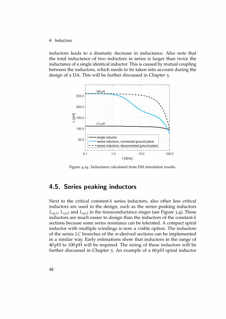
To quantify the performance of the series connection of inductors, thetotal inductance is calculated from EM simulation results. Figure 4.24presents the results. As expected, connecting the ground planes of adjacent
47
4. Inductors
inductors leads to a dramatic decrease in inductance. Also note thatthe total inductance of two inductors in series is larger than twice theinductance of a single identical inductor. This is caused by mutual couplingbetween the inductors, which needs to be taken into account during thedesign of a DA. This will be further discussed in Chapter 5.
0.1 1.0 10.0 100.0
f [GHz]
50.0
100.0
150.0
200.0
250.0
L [
pH
]
single inductor
series inductors, connected ground plane
series inductors, disconnected ground plane
111 pH
260 pH
Figure 4.24.: Inductance calculated from EM simulation results.
4.5. Series peaking inductors
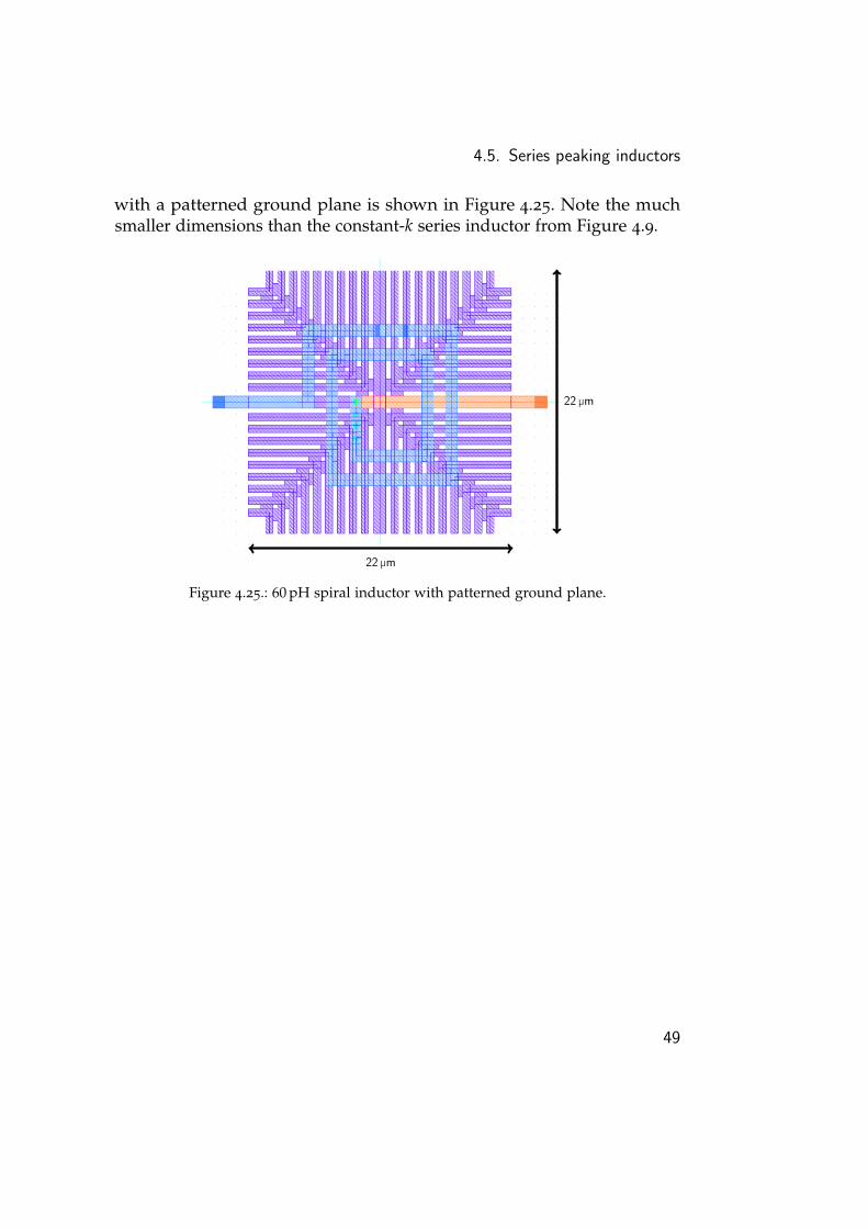
Next to the critical constant-k series inductors, also other less criticalinductors are used in the design, such as the series peaking inductorsLsp,1, Lsp,2 and Lsp,3 in the transconductance stages (see Figure 3.4). Theseinductors are much easier to design than the inductors of the constant-ksections because some series resistance can be tolerated. A compact spiralinductor with multiple windings is now a viable option. The inductorsof the series LC branches of the m-derived sections can be implementedin a similar way. Early estimations show that inductors in the range of40 pH to 100 pH will be required. The sizing of these inductors will befurther discussed in Chapter 5. An example of a 60 pH spiral inductor
48
4.5. Series peaking inductors
with a patterned ground plane is shown in Figure 4.25. Note the muchsmaller dimensions than the constant-k series inductor from Figure 4.9.
22 µm
22 µm
Figure 4.25.: 60 pH spiral inductor with patterned ground plane.
49


5. Design of a DistributedAmplifier
The previous chapters have provided the necessary architecture and build-ing blocks to design a distributed amplifier. This chapter combines theknowledge of these preceding chapters into the design of a distributedamplifier. The design will start from an idealized circuit, after which theaforementioned building blocks are mapped to components in this ideal-ized circuit. Some iterative steps will be necessary to come to an optimallysized design. Table 5.1 summarizes the specifications of the amplifier,which were derived in Chapter 1.
Input signal 200 mVPP PAM4Output swing 2 VPP
Gain 20 dBBandwidth > 30 GHz
Load impedance Zout = 50 Ω
Table 5.1.: DA specifications.
5.1. Distributed amplifier topology
An important characteristic of a DA is the number of transconductancestages N. Initially, the gain of the amplifier will increase linearly by addingmore stages. However, more stages also require longer (lossy) transmissionlines. For large N, an exponential decay along the transmission lines cannotbe compensated by a linear increase in gain. As such, an optimum numberof transconductance stages Nopt exists. This optimum number of stages
51

5. Design of a Distributed Amplifier
Nopt can be derived theoretically [14]; in practice distributed amplifierswith 4 to 7 stages are common [17]. In this thesis, no attempt was madeat finding the optimum number of stages in the available semiconductortechnology. Instead, N = 6 was used, resulting in realistic values for allcomponents.
Based on Subsection 2.2.4, we get to the amplifier topology shown inFigure 5.1. In this circuit, Zin and Zout are defined as
Zin =
√Lin
CinZout =
√Lout
Cout(5.1)
This circuit is the most ideal distributed amplifier, and will serve as adesign goal for the actual amplifier. By continuously identifying the actualdesign with this ideal circuit, as many as possible parasitic capacitancescan be taken into account by assigning them to either Cin or Cout. Thisapproach will be elaborated in the following sections.
5.2. Schematic
Figure 5.2 shows the complete circuit of the designed DA. In this circuit,the N = 6 transconductance stages from Chapter 3 can be recognized. Theinductors of the constant-k sections L0
in and L0out and the series inductors
of the m-derived sections Lmin and Lm
out have important parasitics whichwill be taken into account. To emphasize this, these inductors are drawn ina box. Figure 5.3 clarifies these symbols. The other passives in the circuit,not drawn in a box, also suffer from parasitics. However, these parasiticsare of less importance to the design procedure outlined in Section 5.3.Inevitably, there will be some unintentional coupling between adjacentinductors. This is quantified by the coupling coefficients kin, kB
in, kout andkB
out, and can be taken into account during the design.The capacitors Ceq
in , Ceq,Bin , Ceq
out and Ceq,Bout can be used to equalize the capa-
citance at all nodes, ensuring phase matching and Zout =√
LoutCout
= 50 Ω.
52

5.2. Schematic
(1+
m)
L in 2
1−m
2
2mL i
n
mC
in 2
L in
L in
L in
L in
L in
Cin
Cin
Cin
Cin
Cin
Cin(1
+m)
L in 2
1−m
2
2mL i
n
mC
in 2
X1
X2
X3
X4
X5
X6
sour
ce
(1+
m)
L out 2
1−m
2
2mL o
ut
mC
out
2
L out
L out
L out
L out
L out
Cou
tC
out
Cou
tC
out
Cou
tC
out
g mX
1g m
X2
g mX
3g m
X4
g mX
5
g mX
6
(1+
m)
L out 2
1−m
2
2mL o
ut
mC
out
2
Zou
t
2V0
Zin
Zou
t
Zin
load
Figu
re5.
1.:T
opol
ogy
ofa
6-st
age
DA
base
don
cons
tant
-kan
dm
-der
ived
filte
rse
ctio
ns.
53

5. Design of a Distributed Amplifier
L0 inL0 in
L0 inL0 in
L0 inLm in
1−m
2
2mL i
n
m 2C
in
Lm in
1−m
2
2mL i
n
m 2C
inV
g1
2V0
Zin
1Z
inV
g1
Vin
Ceq
,Bin
Ceq in
Ceq in
Ceq in
Ceq in
Ceq
,Bin
L sp,
1
L sp,
2
L sp,
3
C3
C4
M1
M2
M3
M4
R3
R4
Vg3
Vg4
Vg2
I D
Zts in
Zts ou
t
L sp,
1
L sp,
2
L sp,
3
C3
C4
M1
M2
M3
M4
R3
R4
Vg3
Vg4
Vg2
I D
L sp,
1
L sp,
2
L sp,
3
C3
C4
M1
M2
M3
M4
R3
R4
Vg3
Vg4
Vg2
I D
L sp,
1
L sp,
2
L sp,
3
C3
C4
M1
M2
M3
M4
R3
R4
Vg3
Vg4
Vg2
I D
L sp,
1
L sp,
2
L sp,
3
C3
C4
M1
M2
M3
M4
R3
R4
Vg3
Vg4
Vg2
I D
L sp,
1
L sp,
2
L sp,
3
C3
C4
M1
M2
M3
M4
R3
R4
Vg3
Vg4
Vg2
I D
L0 out
L0 out
L0 out
L0 out
L0 out
Lm out
1−m
2
2mL o
ut
m 2C
out
Lm out 1−
m2
2mL o
ut
m 2C
out
Zou
t
6IDV
DD
2V
out
L ter
mZ
out
Vd4
Ceq
,Bou
tC
eq out
Ceq ou
tC
eq out
Ceq ou
tC
eq,B
out
kB ink i
nk i
nk i
nk i
nkB in
kB out
k out
k out
k out
k out
kB out
Figu
re5.
2.:C
ompl
ete
circ
uit
ofth
ede
sign
edD
A.T
hebo
xed
indu
ctor
sL0 in
,Lm in
,L0 ou
tan
dLm ou
tar
eex
plai
ned
inFi
gure
5.3.
54

5.2. Schematic
The bias currents of all N = 6 transconductance stages are fed to the amp-lifier via the load impedance Zout at the right-hand side of the output TL.Since the total current drawn by the amplifier is limited by the maximumallowed current through the traces of the inductor Lm
out, feeding the ampli-fier using both ends of the output TL is an attractive option. Nevertheless,this requires that the termination impedance Zout at the left-hand side ofthe output TL has to withstand a high DC current, and as such should bephysically very large. This large resistor will then suffer from too muchparasitic capacitance, destroying the high-frequency performance of theamplifier. We conclude that it is better to feed the amplifier only via theload impedance, which is assumed to be ideal. To prevent DC current fromflowing through the termination resistor at the left-hand side of the outputTL, a suitable bias voltage Vd4 (approximately equal to the drain voltageof M4) is applied to serve as signal ground. Now this resistor can be mademuch smaller, reducing the amount of parasitic capacitance. Because thisresistor still has to cope with a 2 VPP voltage swing, an additional inductorLterm is added to counter the remaining parasitic capacitance.
L0in
Rkin
L0in
Ckin Ck
in
Lmin
Rmin
Lmin=
1+m2 Lin
Cmin Cm
in
L0out
Rkout L0
out
Ckout Ck
out
Lmout
Rmout Lm
out=1+m
2 Lout
Cmout Cm
out
Figure 5.3.: Compact representation of the inductors L0in, Lm
in, L0out and Lm
out.
55

5. Design of a Distributed Amplifier
As a final remark, it should be avoided that a DC current flows alongthe input TL. Because of the series resistance of the inductors L0
in and Lmin,
every transistor M1 will see a slightly different gate voltage, resulting inlarge differences among the drain currents. To prevent DC current fromflowing, the termination impedance Zin at the right-hand side of the inputTL is connected to the same bias voltage Vg1 as the source impedance Zinat the left-hand side.
5.3. Design procedure
The design of a DA consists of many iterative steps, which are discussedbelow. This iterative character finds its origin in the fact that the design isbased on the input and output capacitance of a transconductance stage.These capacitances are only known if the sizing of all the componentsof a transconductance stage is known. However, to adequately size atransconductance stage, it is necessary to consider the entire amplifier,of which the design is based on the input and output capacitance of atransconductance stage.
5.3.1. Step 1: Determine Ctsin and Cts
out
The first step in the design procedure consists of determining the inputcapacitance Cts
in and the output capacitance Ctsout of a transconductance
stage. These capacitances depend on the spiral inductors Lsp,1, Lsp,2 andLsp,3, the capacitors C3 and C4, the biasing resistors R3 and R4, and to acertain extent also on the bias voltages Vg2, Vg3, Vg4 and VDD. Since theseare not yet known in this initial step of the design, one has to begin froman educated guess. As a starting point, we design three spiral inductorswith inductances Lsp,1 = 40 pH, Lsp,2 = Lsp,3 = 60 pH. The gate capacitorsare sized as C3 = 50 fF and C4 = 20 fF, the biasing resistors are initializedat R3 = R4 = 1 MΩ.The input impedance of a transconductance stage Zts
in (see Figure 5.2) canbe modelled as a series RC circuit, of which the capacitance Cts
in is shownin Figure 5.4. The increase of the input capacitance at higher frequencies
56
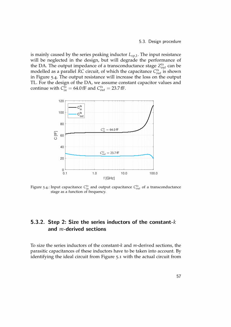
5.3. Design procedure
is mainly caused by the series peaking inductor Lsp,1. The input resistancewill be neglected in the design, but will degrade the performance ofthe DA. The output impedance of a transconductance stage Zts
out can bemodelled as a parallel RC circuit, of which the capacitance Cts
out is shownin Figure 5.4. The output resistance will increase the loss on the outputTL. For the design of the DA, we assume constant capacitor values andcontinue with Cts
in = 64.0 fF and Ctsout = 23.7 fF.
0.1 1.0 10.0 100.0
f [GHz]
0
20
40
60
80
100
120
C [fF
]
Cin
ts
Cout
ts
Ctsin = 64.0 fF
Ctsout = 23.7 fF
Figure 5.4.: Input capacitance Ctsin and output capacitance Cts
out of a transconductancestage as a function of frequency.
5.3.2. Step 2: Size the series inductors of the constant-kand m-derived sections
To size the series inductors of the constant-k and m-derived sections, theparasitic capacitances of these inductors have to be taken into account. Byidentifying the ideal circuit from Figure 5.1 with the actual circuit from
57

5. Design of a Distributed Amplifier
Figure 5.2, we see that
Ctsin + Ceq,B
in + Ckin + Cm
in = Cin (5.2)
Ctsin + Ceq
in + 2Ckin = Cin (5.3)
Ctsout + Ceq,B
out + Ckout + Cm
out = Cout (5.4)
Ctsout + Ceq
out + 2Ckout = Cout (5.5)
The capacitors Ckin, Cm
in, Ckout and Cm
out are explained in Figure 5.3. To sim-plify the design procedure, we will first neglect the effect of inductivecoupling between adjacent inductors. To this end, we put kin = kB
in =
kout = kBout = 0, resulting in Lout = L0
out. To size the series inductors of theconstant-k sections in the output TL, we set
Zout =
√Lout
Cout=
√L0
out
Ctsout + Ceq
out + 2Ckout
= 50 Ω (5.6)
The optimal solution will be the one resulting in the smallest inductor L0out,
because this inductor will have the smallest series resistance. To get to thisoptimal solution, we can put Ceq
out = 0, and carefully tune the inductoruntil it fits the equation. A faster (but suboptimal) solution would be topick a larger inductor, and to increase Ceq
out > 0 until (5.6) is satisfied. Theoptimal design procedure is illustrated in Table 5.2, using the inductor L0
outdrawn in Figure 5.5. The inductor with H = 64 µm fits (5.6) and will beused in the output TL. The output capacitance Cout can now be calculatedfrom (5.5) and equals Cout = 62.3 fF, the output inductance Lout equalsLout = 156 pH.Care must be taken at the outer ends of the constant-k sections. SinceLm
out = 1+m2 Lout = 124.8 pH < Lout = 156 pH, the parasitic capacitance
Cmout = 14.9 fF is also smaller than Ck
out = 19.3 fF. This can be compensatedby using the capacitors Ceq,B
out . From (5.4), we get Ceq,Bout = 4.4 fF.
58
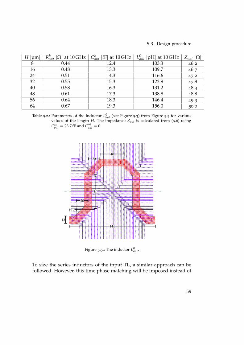
5.3. Design procedure
H [µm] Rkout [Ω] at 10 GHz Ck
out [fF] at 10 GHz L0out [pH] at 10 GHz Zout [Ω]
8 0.44 12.4 103.3 46.216 0.48 13.3 109.7 46.724 0.51 14.3 116.6 47.232 0.55 15.3 123.9 47.840 0.58 16.3 131.2 48.348 0.61 17.3 138.8 48.856 0.64 18.3 146.4 49.364 0.67 19.3 156.0 50.0
Table 5.2.: Parameters of the inductor L0out (see Figure 5.3) from Figure 5.5 for various
values of the length H. The impedance Zout is calculated from (5.6) usingCts
out = 23.7 fF and Ceqout = 0.
144
12
20
2040
12
H
Figure 5.5.: The inductor L0out.
To size the series inductors of the input TL, a similar approach can befollowed. However, this time phase matching will be imposed instead of
59

5. Design of a Distributed Amplifier
a particular value of Zin. From the phase matching condition LinCin =LoutCout, we get to
L0in(C
tsin + Ceq
in + 2Ckin) = LoutCout (5.7)
using Lin = L0in and (5.3). The designed inductor which fits the equation
for Ceqin = 0 is characterized by Ck
in = 12.9 fF and Lin = L0in = 109 pH.
From (5.3), we get Cin = 89.8 fF. The series inductors of the m-derivedsections are sized at Lm
in = 1+m2 Lin = 87.2 fF with Cm
in = 7.5 fF. Using thesevalues in (5.2), we finally get Ceq,B
in = 5.4 fF. Table 5.3 gives a summary ofthe inductor sizing. Since Zin = 35 Ω < 50 Ω, an input buffer is requiredto match the amplifier to a 50 Ω source. Due to time constraints, this inputbuffer is not further discussed.
Ctsin 64.0 fF Cts
out 23.7 fFCk
in 12.9 fF Ckout 19.3 fF
Cmin 7.5 fF Cm
out 14.9 fFCeq
in 0 fF Ceqout 0 fF
Ceq,Bin 5.4 fF Ceq,B
out 4.4 fFCin 89.8 fF Cout 62.3 fFL0
in 109 pH L0out 156 pH
Lin 109 pH Lout 156 pHZin 35 Ω Zout 50 Ω
Table 5.3.: Summary of inductor sizing.
5.3.3. Step 3: Verify the performance of the amplifierthrough S-parameter simulation
To verify the performance of the amplifier, S-parameters are simulatedusing accurate models for all passives and transistors. Since Zin = 35 Ω <50 Ω, the S-parameters are normalized w.r.t. the impedances R1 = 35 Ωand R2 = 50 Ω, and should be interpreted accordingly. Figure 5.6a reveals
60

5.3. Design procedure
excellent matching over the entire frequency range: |S11| < −10 dB forf < 92.9 GHz and |S22| < −10 dB for f < 86.0 GHz.The simulation results of S21 are plotted in Figure 5.6b. The amplifier hasa gain of 19.2 dB with a −1 dB bandwidth of 49.7 GHz and a −3 dB band-width of 61.0 GHz. The frequency response of the amplifier is relativelyflat over the entire bandwidth, suggesting that the initial guess of theseries peaking inductors Lsp,1, Lsp,2 and Lsp,3 was a good choice. If thefrequency response is not flat, Step 1 through Step 3 should be repeateduntil the frequency response is flat. In practice one can try different sets ofvalues for Lsp,1, Lsp,2, Lsp,3, and check if the input capacitance Cts
in andthe output capacitance Cts
out of the transconductance stage have changedsignificantly. If this would be the case, Step 1 through Step 3 should be re-peated. Every iteration requires the redesign of multiple inductors, whichis a lengthy process. To speed up the design procedure, EM simulationscan be limited to a single frequency, and the results can be used to createa lumped model of the inductor (see Figure 4.17). Because of the variationin the resistance and the inductance of the inductor at high frequencies(see Figure 4.12), a broadband EM simulation should always be performedto verify the high frequency behavior. Another option is to create tables(such as Table 5.2) of suitable inductor topologies.The group delay shown in Figure 5.6b suffers from variations both at lowfrequencies and at high frequencies. The variation at high frequencies isinherent to constant-k filters (see Figure 2.10c), but can be tuned by a suit-able choice of Lsp,1, Lsp,2, Lsp,3. The variation at low frequencies can beattributed to the modified CG transistors of the transconductance stages,more specifically to the biasing resistors R3 and R4. This low frequencydistortion can be reduced by sizing these resistors (much) larger than theircurrent value of 1 MΩ.The Rollett stability factor reveals that the amplifier is unconditionallystable: k > 1, ∀ f . However, a more detailed analysis of all individualtransistors is necessary to guarantee stability. Due to time constraints, thiswas not investigated.
61

5. Design of a Distributed Amplifier
106
107
108
109
1010
1011
f [Hz]
-50
-40
-30
-20
-10
0[d
B]
S11
S22
(a) Simulation of S11 and S22. The DA isexcellently matched over the entirefrequency range.
106
107
108
109
1010
1011
f [Hz]
10
12
14
16
18
20
|S21| [d
B]
0
10
20
30
40
50
gro
up
de
lay [
ps]
19.2 dB
25.3 ps
−1 dB at 49.7GHz
−3 dB at 61.0GHz
(b) Simulation of S21. The amplifierhas a flat frequency response up to61.0 GHz.
Figure 5.6.: S-parameter simulation using accurate models for all passives and transistors.
5.3.4. Step 4: Voltage swing over the cascode transistors
As explained in Chapter 3, the top CG transistors of the cascode weremodified by adding the capacitors C3 and C4 to allow a large voltageswing of 2 VPP over the transconductance stages. These capacitors, to-gether with the bias voltages Vg2, Vg3, Vg4 and VDD, should be tuned tooptimally distribute the voltage swing over all transistors of the cascode.The drain-source voltage of every transistor should at all times be higherthan Vsat ≈ 200 mV to maintain pentode operation, and should be lowerthan, say, 1 V to prevent breakdown. The initial values chosen in Step1, repeated in Table 5.4, provide an excellent distribution of the voltageswing over the cascode. This is illustrated by means of an example inFigure 5.7, where a 10 GBaud 200 mVPP PAM4 signal is applied to theamplifier. Using biasing resistors of R3 = R4 = 1 MΩ, the amplifier canwithstand a 200 mVPP 10 MHz input sine wave.If the initial values of the components and the bias voltages chosen inStep 1 do not result in an adequate distribution of the voltage swingover the transistors of the cascode, Step 1 through Step 4 should berepeated until a solution is found. In practice it can suffice to tuneC3, C4, Vg2, Vg3, Vg4, VDD until a good voltage distribution is found, and
62
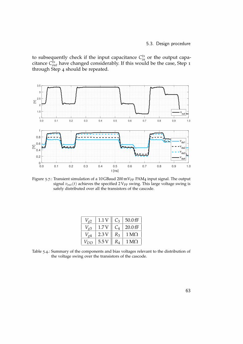
5.3. Design procedure
to subsequently check if the input capacitance Ctsin or the output capa-
citance Ctsout have changed considerably. If this would be the case, Step 1
through Step 4 should be repeated.
0.0 0.1 0.2 0.3 0.4 0.5 0.6 0.7 0.8 0.9 1.01
1.5
2
2.5
3
3.5
[V]
vout
0.0 0.1 0.2 0.3 0.4 0.5 0.6 0.7 0.8 0.9 1.0
t [ns]
0
0.2
0.4
0.6
0.8
1
[V]
vds1
vds2
vds3
vds4
Figure 5.7.: Transient simulation of a 10 GBaud 200 mVPP PAM4 input signal. The outputsignal vout(t) achieves the specified 2 VPP swing. This large voltage swing issafely distributed over all the transistors of the cascode.
Vg2 1.1 V C3 50.0 fFVg3 1.7 V C4 20.0 fFVg4 2.3 V R3 1 MΩVDD 5.5 V R4 1 MΩ
Table 5.4.: Summary of the components and bias voltages relevant to the distribution ofthe voltage swing over the transistors of the cascode.
63
5. Design of a Distributed Amplifier
5.3.5. Step 5: Inductive coupling between adjacentinductors
The last step in the design procedure discusses the inductive couplingbetween adjacent inductors. To keep the analysis manageable, only thecoupling between adjacent constant-k series inductors will be considered.A complete analysis of this problem would require the analysis of themodified constant-k filter section shown in Figure 5.8. Since this turns outto be quite complex, a more ad hoc approach will be followed [4]. Weassume that the ideal circuit from Figure 5.1 is still valid, and define theeffective input inductance Lin and the effective output inductance Loutas
Lin = (1 + 2kin)L0in (5.8)
Lout = (1 + 2kout)L0out (5.9)
where the coupling coefficients kin > 0 and kout > 0 are indicated inFigure 5.2. These expressions are only valid for the inductors L0
in and L0out
in the bulk of the TL, not for those at the boundaries adjacent to Lmin or
Lmout. However, since the series m-derived inductors Lm
in and Lmout are of
comparable size as the series constant-k inductors L0in and L0
out, these willhave a similar layout, and as such kin ≈ kB
in and kout ≈ kBout, resulting
in a similar effective inductance for the inductors at the boundaries. Tocompensate for the inductive coupling, only the inductors L0
in and L0out
will be resized according to (5.8) and (5.9). Resizing the series m-derivedinductors can result in an additional performance gain, but will not bediscussed due to time constraints. By compensating the inductors forthe parasitic inductive coupling, the performance of the amplifier canpotentially increase since smaller inductors have less parasitics. Amongstthese parasitics are the capacitances Ck
in and Ckout, demanding a revisit of
Step 2. To simplify the design procedure, we will maintain the originalvalues of Lin = 109 pH, Cin = 89.8 fF, Lout = 156 pH and Cout = 62.3 fF,and compensate the reduction of Ck
in and Ckout by the addition of the
capacitors Ceqin and Ceq
out. Table 5.5 summarizes the redesign of the inductors.
To accurately simulate the inductive coupling between adjacent inductors,
64
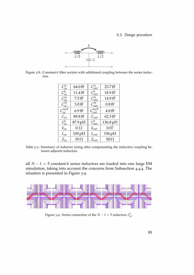
5.3. Design procedure
L/2 L/2C
k
Figure 5.8.: Constant-k filter section with additional coupling between the series induc-tors.
Ctsin 64.0 fF Cts
out 23.7 fFCk
in 11.4 fF Ckout 18.9 fF
Cmin 7.5 fF Cm
out 14.9 fFCeq
in 3.0 fF Ceqout 0.8 fF
Ceq,Bin 6.9 fF Ceq,B
out 4.8 fFCin 89.8 fF Cout 62.3 fFL0
in 87.9 pH L0out 136.8 pH
kin 0.12 kout 0.07Lin 109 pH Lout 156 pHZin 35 Ω Zout 50 Ω
Table 5.5.: Summary of inductor sizing after compensating the inductive coupling be-tween adjacent inductors.
all N − 1 = 5 constant-k series inductors are loaded into one large EMsimulation, taking into account the concerns from Subsection 4.4.4. Thesituation is presented in Figure 5.9.
Figure 5.9.: Series connection of the N − 1 = 5 inductors L0in.
65
5. Design of a Distributed Amplifier
Figure 5.10 shows the S-parameter simulation results for three cases: (1)the case where coupling between adjacent inductors is not simulated (thisis a reprint of Figure 5.6), (2) the case where coupling is taken into accountin the simulation but not in the design, and finally (3) the case where thecoupling is compensated in the design. The coupling is very detrimentalfor matching, which can only slightly be restored by resizing the inductors.Overall the matching of the amplifier is better than −13 dB at both theinput and the output over the entire frequency range. The flatness of thegain and the group delay has actually improved by the introduction ofinductive coupling, again illustrating that this parasitic inductive couplingis not entirely disadvantageous. The amplifier ultimately achieves a −1 dBbandwidth of 46.8 GHz and a −3 dB bandwidth of 60.0 GHz, with a groupdelay variation of up to 3.6 ps at 60 GHz. In all three cases, the Rollettstability factor is larger than 1: k > 1 ∀ f .
5.3.6. Time domain simulation results
To estimate the performance of the amplifier, eye diagrams are generatedat various baud rates. Figure 5.11 through Figure 5.16 show the resultsfor transmission speeds from 20 GBaud up to 80 GBaud. These eye dia-grams were generated using a 200 mVPP PAM4 PRBS23 input signal witha simulation time of 20000 symbol periods. It is observed that the ampli-fier achieves the specified 2 VPP voltage swing, however, with noticeablecompression of the upper voltage range. This is indicated in Figure 5.11.This non-linearity is primarily caused by the current limit imposed bythe metal traces of the output constant-k series inductors, as explained inSubsection 3.2.2.
The amplifier has a DC power consumption of PDC = 330 mW. Thiscorresponds to 2.06 pJ/b using 80 GBaud PAM4.
66

5.3. Design procedure
106
107
108
109
1010
1011
f [Hz]
-50
-40
-30
-20
-10
0
|S1
1| [d
B]
uncoupled
coupled, uncompensated
coupled, compensated
(a) S11
106
107
108
109
1010
1011
f [Hz]
-50
-40
-30
-20
-10
0
|S2
2| [d
B]
uncoupled
coupled, uncompensated
coupled, compensated
(b) S22
106
107
108
109
1010
1011
f [Hz]
10
12
14
16
18
20
|S2
1| [d
B]
uncoupled
coupled, uncompensated
coupled, compensated
(c) S21
106
107
108
109
1010
1011
f [Hz]
20
25
30
35
gro
up
de
lay [
ps]
uncoupled
coupled, uncompensated
coupled, compensated
(d) group delay
Figure 5.10.: S-parameter simulation using accurate models for all passives and transis-tors.
v out(t)
[V]
1.5
2.0
2.5
3.0
3.5
t [ps]0.0 50.0 100.0 150.0
3.35V
2.80V
2.10V
1.35V
550mV
700mV
750mV
Figure 5.11.: 20 GBaud. The compression of the upper voltage range is indicated in thefigure.
67
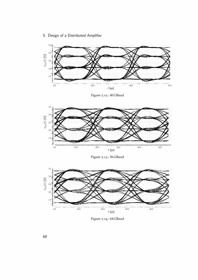
5. Design of a Distributed Amplifier
v out(t)
[V]
1.5
2.0
2.5
3.0
3.5
t [ps]0.0 25.0 50.0 75.0
Figure 5.12.: 40 GBaud
v out(t)
[V]
1.5
2.0
2.5
3.0
3.5
t [ps]0.0 10.0 20.0 30.0 40.0 50.0
Figure 5.13.: 56 GBaud
v out(t)
[V]
1.5
2.0
2.5
3.0
3.5
t [ps]0.0 10.0 20.0 30.0 40.0
Figure 5.14.: 64 GBaud
68
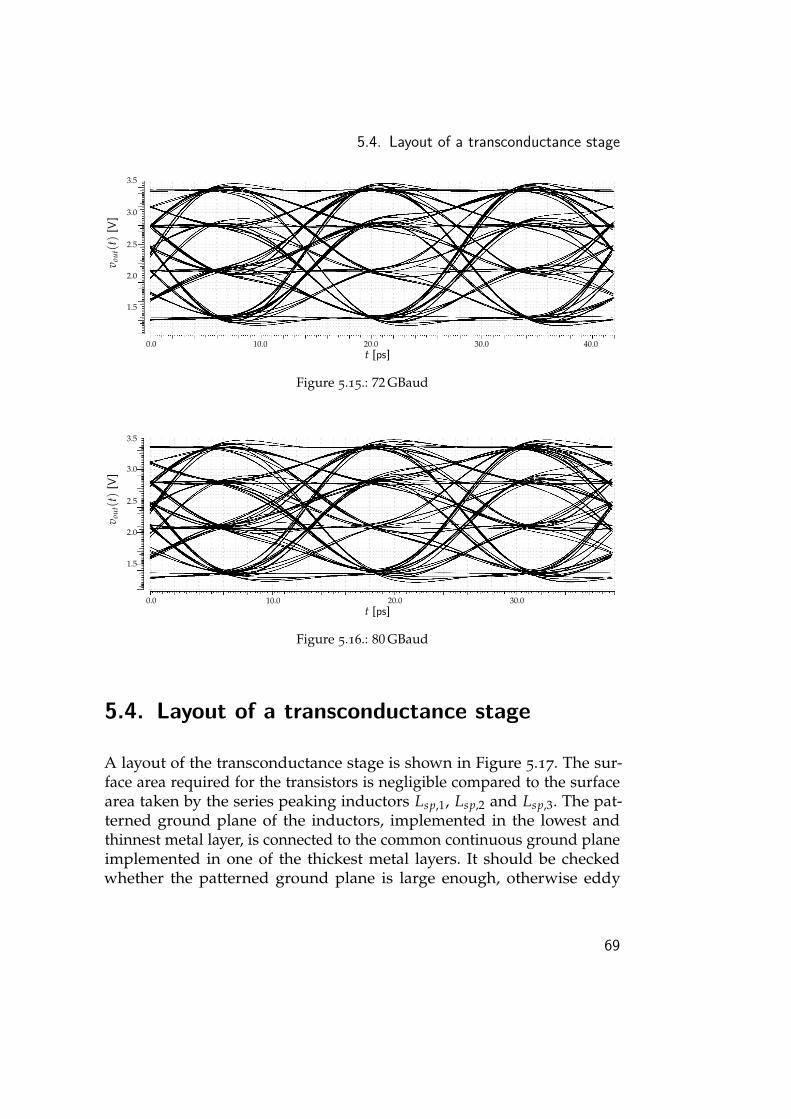
5.4. Layout of a transconductance stage
v out(t)
[V]
1.5
2.0
2.5
3.0
3.5
t [ps]0.0 10.0 20.0 30.0 40.0
Figure 5.15.: 72 GBaud
v out(t)
[V]
1.5
2.0
2.5
3.0
3.5
t [ps]0.0 10.0 20.0 30.0
Figure 5.16.: 80 GBaud
5.4. Layout of a transconductance stage
A layout of the transconductance stage is shown in Figure 5.17. The sur-face area required for the transistors is negligible compared to the surfacearea taken by the series peaking inductors Lsp,1, Lsp,2 and Lsp,3. The pat-terned ground plane of the inductors, implemented in the lowest andthinnest metal layer, is connected to the common continuous ground planeimplemented in one of the thickest metal layers. It should be checkedwhether the patterned ground plane is large enough, otherwise eddy
69

5. Design of a Distributed Amplifier
currents can flow through the continuous ground plane around the pat-terned ground plane. The gate capacitors C3 and C4 require a very good(that is low impedance) signal ground, and are therefore connected to theground plane itself, instead of any other biasing voltage. The physicallylong resistors R3 and R4 are rolled up to make the layout more compact.
5.5. Coupling between the input and outputtransmission lines
A DA consists of two transmission lines, which were assumed to be iso-lated from each other in the previous sections. Nevertheless, in realitythere will be some coupling between both lines. If this coupling is not neg-ligible, currents generated on the output TL will couple back to the inputTL. This can potentially degrade the matching of the amplifier or evendestabilize the amplifier. To investigate this effect, the constant-k seriesinductors L0
in and L0out of both the input TL and the output TL are loaded
into the same EM simulation. The situation is sketched in Figure 5.18,where the distance D between both lines is indicated in the figure. Toquantify the effect of coupling between the input TL and the output TL,S11, S21, S12 and the k-stability factor are plotted in Figure 5.19 for variousdistances D between the lines. The case of D = ∞ corresponds to the as-sumption of no coupling (coupling between adjacent series inductors wastaken into account and was compensated in the design), and was alreadyprinted in Figure 5.10. The amplifier suffers from bad matching, largegain variations and instability for the minimal distance D = 120 µm (seealso Figure 5.17). The performance of the amplifier is only similar to thecase of D = ∞ for D > 300 µm. To achieve sufficient spacing between thelines, the series peaking inductors Lsp,1, Lsp,2 and Lsp,3 can be (partially)unrolled.One could wonder if it is possible to shield both transmission lines fromeach other by using stacks of vias. Sadly, this has proven to be very com-putationally intensive to simulate, even with considerable simplifications,and as a result requires further investigation.
70
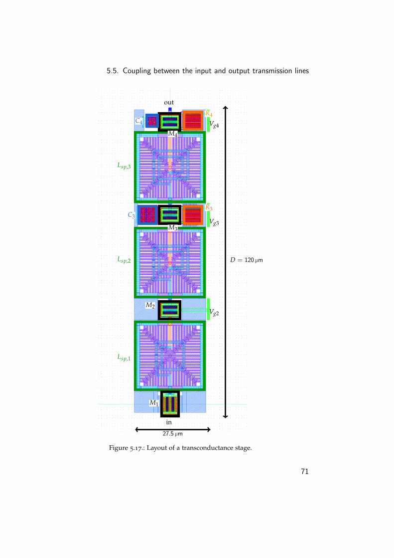
5.5. Coupling between the input and output transmission lines
D = 120 µm
27.5 µm
Lsp,1
Lsp,2
Lsp,3
M1
M2
M3
M4
C3
C4
R3
R4
in
out
Vg2
Vg3
Vg4
Figure 5.17.: Layout of a transconductance stage.
71

5. Design of a Distributed Amplifier
D
720 µm
Figure 5.18.: Layout of the constant-k series inductors L0in and L0
out.
72
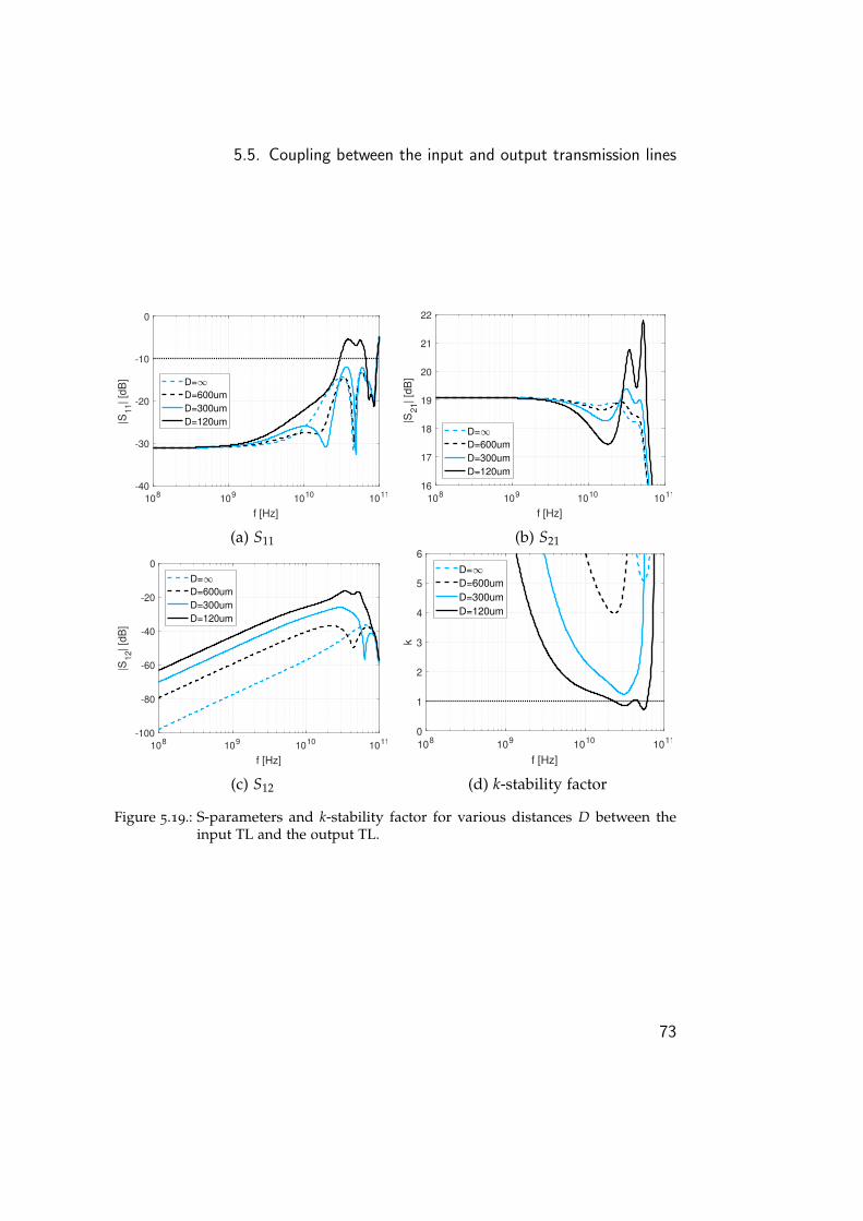
5.5. Coupling between the input and output transmission lines
108
109
1010
1011
f [Hz]
-40
-30
-20
-10
0
|S1
1| [d
B] D=
D=600um
D=300um
D=120um
(a) S11
108
109
1010
1011
f [Hz]
16
17
18
19
20
21
22
|S2
1| [d
B]
D=
D=600um
D=300um
D=120um
(b) S21
108
109
1010
1011
f [Hz]
-100
-80
-60
-40
-20
0
|S1
2| [d
B]
D=
D=600um
D=300um
D=120um
(c) S12
108
109
1010
1011
f [Hz]
0
1
2
3
4
5
6
k
D=
D=600um
D=300um
D=120um
(d) k-stability factor
Figure 5.19.: S-parameters and k-stability factor for various distances D between theinput TL and the output TL.
73

6. Conclusions and Future Work
The goal of this master’s dissertation was to design an amplifier for drivingoptical modulators used in intra data center communication. This drivershould therefore have a very large bandwidth (> 30 GHz), and should beable to withstand the large voltage swing (2 VPP) necessary to drive thesemodulators. This chapter concludes this thesis by presenting an overviewof the obtained results, and suggesting some future work.
6.1. Results
To meet the given specifications, a distributed amplifier was designedin a sub-micron CMOS technology. The design consists of two largebuilding blocks which need to be combined: transconductance stagesand inductors. The transconductance stages were implemented as triplecascode circuits, however some adjustments were necessary to makethe amplifier compatible with large output voltage swings. By placingcapacitors between the gates of the CG transistors and signal ground, thegate voltage of these transistors is allowed to vary, thereby preventingtransistor breakdown. To interconnect these transconductance stages, largehigh-quality inductors are required. These inductors should be shieldedfrom the lossy semiconductor substrate to prevent considerable lossesand to keep the performance of the amplifier within the specifications.EM simulations revealed that this ground plane should be patterned toprevent eddy currents from reducing the inductance of the structure. Adistributed amplifier requires inductors with low series resistance and aconstant, capacitive only, parasitic shunt impedance to the substrate.
75

6. Conclusions and Future Work
A DA can be designed by carefully combining the inductors and transcon-ductance stages. An iterative design procedure was devised to guaranteephase matching and Zout = 50 Ω by including all possible parasitic capaci-tances into the design. Furthermore, inductive coupling between adjacentinductors was also considered, and a solution was proposed to overcomesome of the detrimental effects.
The designed amplifier achieves a gain of 19 dB over a bandwidth of60 GHz, with input and output matching better than −13 dB over theentire frequency range. By designing the circuits to distribute the outputvoltage swing over various transistors, a 50 Ω load can safely be driven bya 2 VPP PAM4 signal. The driver ultimately achieves transmission speedsup to 80 GBaud PAM4, corresponding to a bit rate of 160 Gb/s. With apower consumption of 330 mW, this comes down to 2.06 pJ/b.
6.2. Future work
Since integrated circuit design is a never-ending process, some concernsand problems are inevitably left to be discussed in the future. Some of theremaining challenges are listed below.
• The Rollett stability factor k is larger than 1 for all frequencies,indicating that the amplifier is unconditionally stable. However, amore detailed analysis of every individual transistor is required toguarantee stability.• Due to the presence of the biasing resistors R3 and R4, there is a
large variation in the group delay at lower frequencies. However,no such variations occur in |S21|, suggesting that the effect on a bitstream is more complex than simply DC wander [15].• Inductive coupling between adjacent inductors was already dis-
cussed in Subsection 5.3.5, but deserves a more rigorous analysis.The coupling between the input TL and the output TL, and how toprevent this via proper shielding, requires more investigation.• The performance of the amplifier could be further enhanced by
optimizing the sizing of the cascode transistors.
76

6.2. Future work
• A layout of the transconductance stages and the inductors wasalready made. This layout needs to be further completed by addingthe termination impedances, ground and supply planes, etc. Pa-rasitics can be extracted from the layout and taken into account inpost-layout simulations.• Monte-Carlo simulations can be performed to check the sensitivity
of the amplifier to process variations.• Since the input impedance of the amplifier is Zin = 35 Ω, an input
buffer is required to match the amplifier to 50 Ω equipment.• The number of stages was chosen at N = 6. An analysis of the
available technology is required to check if this is the best choice foran amplifier with the given specifications.
77


Bibliography
[1] M. S. Dadash, D. Harame, and S. P. Voiniaescu. “Large-Swing 22nmSi/SiGe FDSOI Stacked Cascodes for 56GBaud Drivers and 5GPAs.” In: 2018 IEEE BiCMOS and Compound Semiconductor IntegratedCircuits and Technology Symposium (BCICTS). Oct. 2018, pp. 267–270.doi: 10.1109/BCICTS.2018.8550932 (cit. on p. 25).
[2] C. C. Enz and E. A. Vittoz. “CMOS low-power analog circuit design.”In: Emerging Technologies: Designing Low Power Digital Systems. May1996, pp. 79–133. doi: 10.1109/ETLPDS.1996.508872 (cit. on p. 23).
[3] E. L. Ginzton et al. “Distributed Amplification.” In: Proceedings ofthe IRE 36.8 (Aug. 1948), pp. 956–969. issn: 0096-8390. doi: 10.1109/JRPROC.1948.231624 (cit. on p. 1).
[4] Yu-Jiu Wang and A. Hajimiri. “A compact low-noise weighted dis-tributed amplifier in CMOS.” In: 2009 IEEE International Solid-StateCircuits Conference - Digest of Technical Papers. Feb. 2009, 220–221,221a. doi: 10.1109/ISSCC.2009.4977387 (cit. on p. 64).
[5] Keysight Momentum. url: https://www.keysight.com/en/pc-1887116 / momentum - 3d - planar - em - simulator ? cc = US & lc = eng
(visited on 05/06/2019) (cit. on p. 38).
[6] Y. K. Koutsoyannopoulos and Y. Papananos. “Systematic analysisand modeling of integrated inductors and transformers in RF ICdesign.” In: IEEE Transactions on Circuits and Systems II: Analog andDigital Signal Processing 47.8 (Aug. 2000), pp. 699–713. issn: 1057-7130. doi: 10.1109/82.861403 (cit. on p. 34).
[7] W. B. Kuhn and N. M. Ibrahim. “Analysis of current crowding effectsin multiturn spiral inductors.” In: IEEE Transactions on MicrowaveTheory and Techniques 49.1 (Jan. 2001), pp. 31–38. issn: 0018-9480. doi:10.1109/22.899959 (cit. on p. 40).
79

Bibliography
[8] J. R. Long and M. A. Copeland. “Modeling of monolithic induc-tors and transformers for silicon RFIC design.” In: Proceedings of1995 IEEE MTT-S International Topical Symposium on Technologies forWireless Applications (Conjunction with INTER COMM’95). Feb. 1995,pp. 129–134. doi: 10.1109/MTTTWA.1995.512338 (cit. on pp. 33, 36).
[9] J. R. Long and M. A. Copeland. “The modeling, characterization, anddesign of monolithic inductors for silicon RF IC’s.” In: IEEE Journalof Solid-State Circuits 32.3 (Mar. 1997), pp. 357–369. issn: 0018-9200.doi: 10.1109/4.557634 (cit. on p. 31).
[10] K. B. Niclas et al. “On Theory and Performance of Solid-State Mi-crowave Distributed Amplifiers.” In: IEEE Transactions on MicrowaveTheory and Techniques 31.6 (June 1983), pp. 447–456. issn: 0018-9480.doi: 10.1109/TMTT.1983.1131524 (cit. on p. 85).
[11] G. Nikandish and A. Medi. “Unilateralization of MMIC DistributedAmplifiers.” In: IEEE Transactions on Microwave Theory and Techniques62.12 (Dec. 2014), pp. 3041–3052. issn: 0018-9480. doi: 10.1109/TMTT.2014.2361341 (cit. on p. 9).
[12] G. Nikandish, R. B. Staszewski, and A. Zhu. “The (R)evolution ofDistributed Amplifiers: From Vacuum Tubes to Modern CMOS andGaN ICs.” In: IEEE Microwave Magazine 19.4 (June 2018), pp. 66–83.issn: 1527-3342. doi: 10.1109/MMM.2018.2813838 (cit. on p. 1).
[13] S. Pornpromlikit et al. “A Watt-Level Stacked-FET Linear PowerAmplifier in Silicon-on-Insulator CMOS.” In: IEEE Transactions onMicrowave Theory and Techniques 58.1 (Jan. 2010), pp. 57–64. issn:0018-9480. doi: 10.1109/TMTT.2009.2036323 (cit. on p. 28).
[14] David M. Pozar. Microwave Engineering. 4th ed. John Wiley & Sons,Inc., 2012 (cit. on pp. 14, 31, 52).
[15] Behzad Razavi. Design of Integrated Circuits for Optical Communica-tions. 2nd ed. John Wiley & Sons, Inc., 2012 (cit. on p. 76).
[16] Behzad Razavi. RF Microelectronics. 2nd ed. Prentice Hall, 2012 (cit.on pp. 34, 36, 39, 40, 42).
[17] Eduard Sackinger. Broadband Circuits for Optical Fiber Communication.John Wiley & Sons, Inc., 2005 (cit. on p. 52).
80

Bibliography
[18] S. Shekhar, J. S. Walling, and D. J. Allstot. “Bandwidth ExtensionTechniques for CMOS Amplifiers.” In: IEEE Journal of Solid-StateCircuits 41.11 (Nov. 2006), pp. 2424–2439. issn: 0018-9200. doi: 10.1109/JSSC.2006.883336 (cit. on p. 29).
[19] Thomas T. Y. Wong. Fundamentals of Distributed Amplification. ArtechHouse, 1993 (cit. on pp. 9, 14, 85).
81


Appendix
83

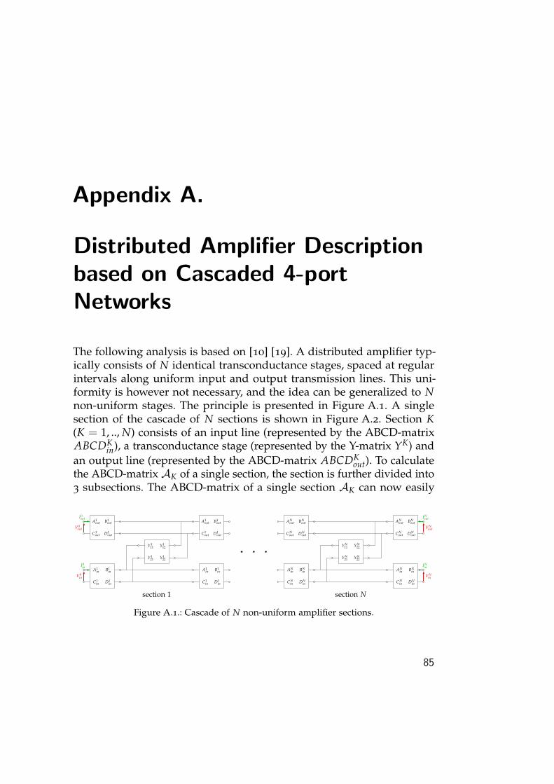
Appendix A.
Distributed Amplifier Descriptionbased on Cascaded 4-portNetworks
The following analysis is based on [10] [19]. A distributed amplifier typ-ically consists of N identical transconductance stages, spaced at regularintervals along uniform input and output transmission lines. This uni-formity is however not necessary, and the idea can be generalized to Nnon-uniform stages. The principle is presented in Figure A.1. A singlesection of the cascade of N sections is shown in Figure A.2. Section K(K = 1, .., N) consists of an input line (represented by the ABCD-matrixABCDK
in), a transconductance stage (represented by the Y-matrix YK) andan output line (represented by the ABCD-matrix ABCDK
out). To calculatethe ABCD-matrix AK of a single section, the section is further divided into3 subsections. The ABCD-matrix of a single section AK can now easily
A1out B1
out
C1out D1
out
A1out B1
out
C1out D1
out
Y111 Y1
12
Y121 Y1
22
A1in B1
in
C1in D1
in
A1in B1
in
C1in D1
in
ANout BN
out
CNout DN
out
ANout BN
out
CNout DN
out
YN11 YN
12
YN21 YN
22
ANin BN
in
CNin DN
in
ANin BN
in
CNin DN
in
V0out
V0in
I0out
I0in
VNout
VNin
INout
INin
section 1 section N
Figure A.1.: Cascade of N non-uniform amplifier sections.
85
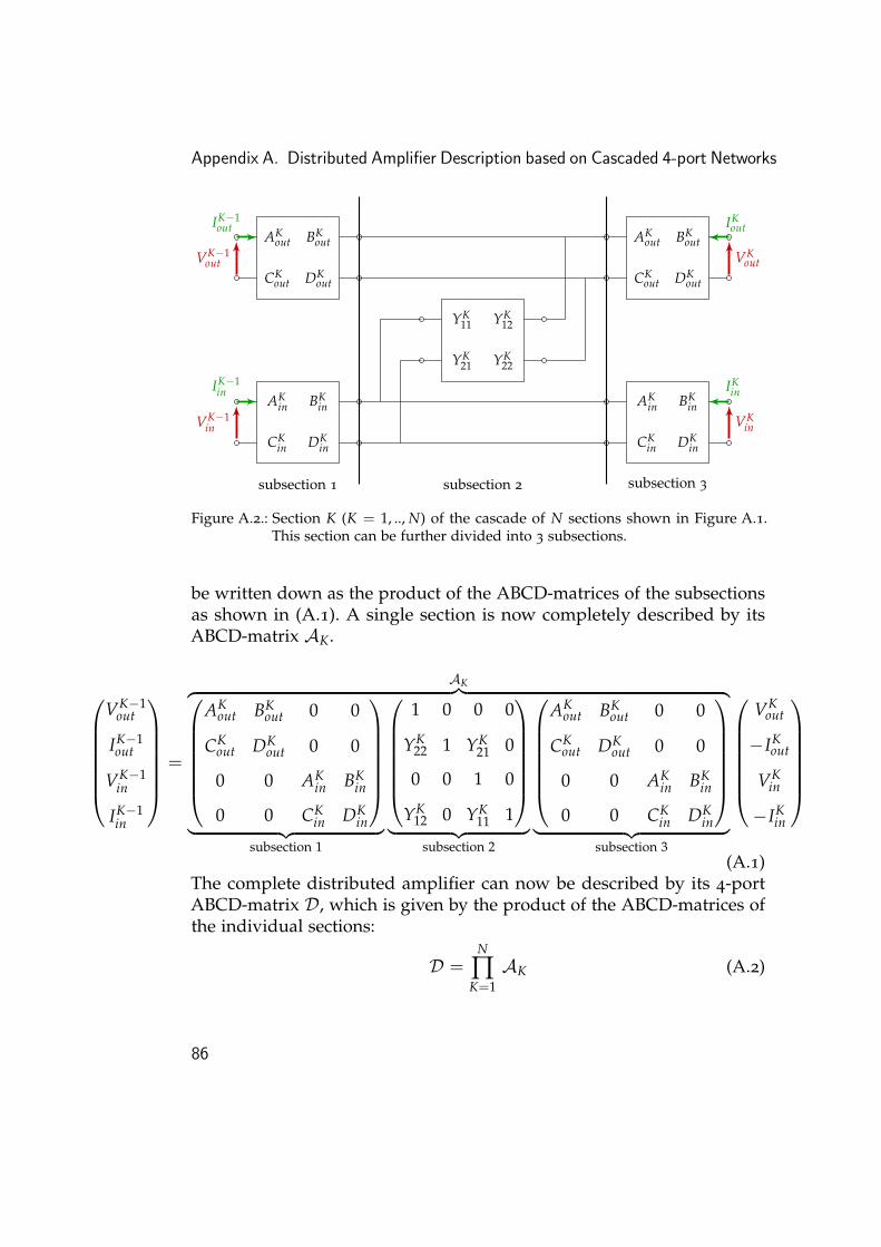
Appendix A. Distributed Amplifier Description based on Cascaded 4-port Networks
AKout BK
out
CKout DK
out
AKout BK
out
CKout DK
out
YK11 YK
12
YK21 YK
22
AKin BK
in
CKin DK
in
AKin BK
in
CKin DK
in
subsection 1 subsection 2 subsection 3
VK−1out
VK−1in
VKout
VKin
IK−1out
IK−1in
IKout
IKin
Figure A.2.: Section K (K = 1, .., N) of the cascade of N sections shown in Figure A.1.This section can be further divided into 3 subsections.
be written down as the product of the ABCD-matrices of the subsectionsas shown in (A.1). A single section is now completely described by itsABCD-matrix AK.
VK−1out
IK−1out
VK−1in
IK−1in
=
AK︷ ︸︸ ︷
AKout BK
out 0 0
CKout DK
out 0 0
0 0 AKin BK
in
0 0 CKin DK
in
︸ ︷︷ ︸subsection 1
1 0 0 0
YK22 1 YK
21 0
0 0 1 0
YK12 0 YK
11 1
︸ ︷︷ ︸subsection 2
AKout BK
out 0 0
CKout DK
out 0 0
0 0 AKin BK
in
0 0 CKin DK
in
︸ ︷︷ ︸subsection 3
VKout
−IKout
VKin
−IKin
(A.1)The complete distributed amplifier can now be described by its 4-portABCD-matrix D, which is given by the product of the ABCD-matrices ofthe individual sections:
D =N
∏K=1AK (A.2)
86
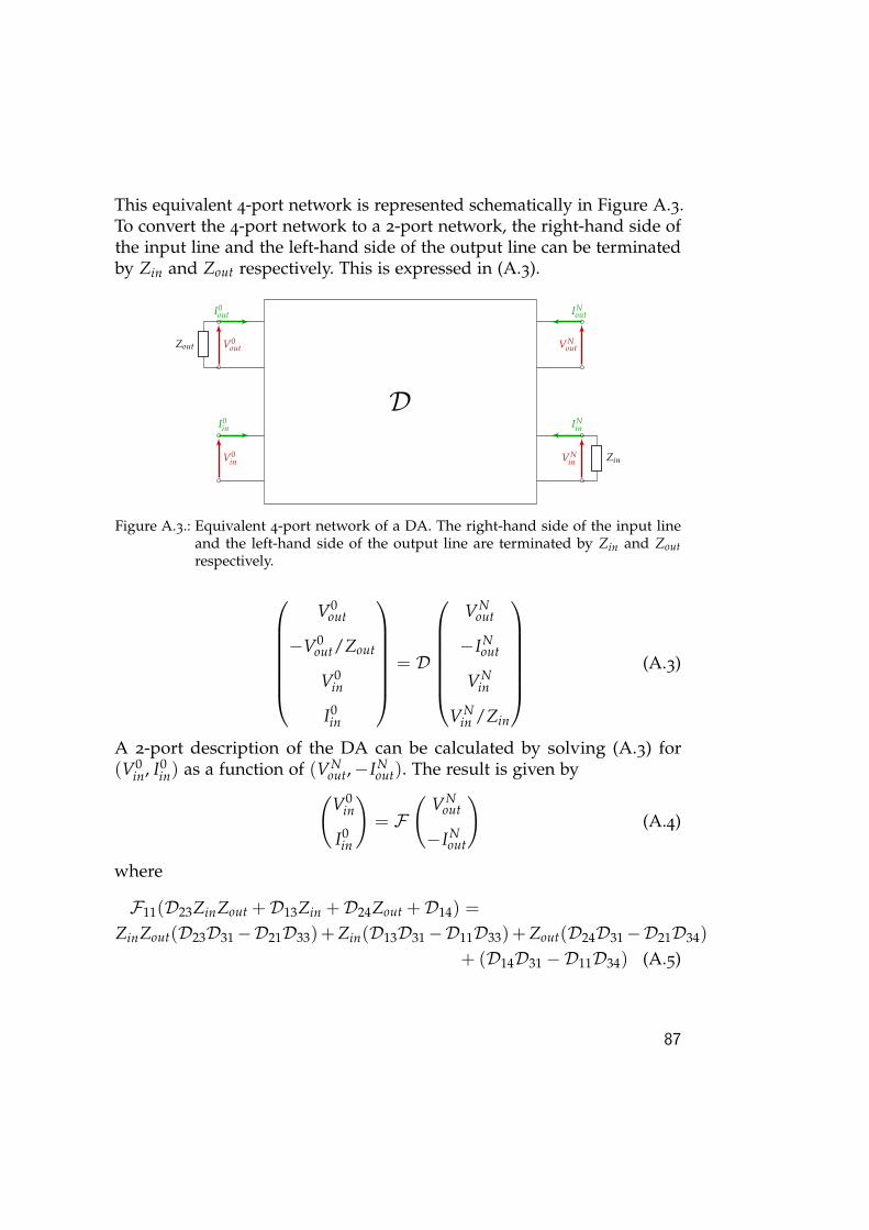
This equivalent 4-port network is represented schematically in Figure A.3.To convert the 4-port network to a 2-port network, the right-hand side ofthe input line and the left-hand side of the output line can be terminatedby Zin and Zout respectively. This is expressed in (A.3).
D
V0out
V0in
I0out
I0in
VNout
VNin
INout
INin
Zout
Zin
Figure A.3.: Equivalent 4-port network of a DA. The right-hand side of the input lineand the left-hand side of the output line are terminated by Zin and Zoutrespectively.
V0out
−V0out/Zout
V0in
I0in
= D
VNout
−INout
VNin
VNin /Zin
(A.3)
A 2-port description of the DA can be calculated by solving (A.3) for(V0
in, I0in) as a function of (VN
out,−INout). The result is given by
(V0
in
I0in
)= F
(VN
out
−INout
)(A.4)
where
F11(D23ZinZout +D13Zin +D24Zout +D14) =
ZinZout(D23D31−D21D33)+Zin(D13D31−D11D33)+Zout(D24D31−D21D34)
+ (D14D31 −D11D34) (A.5)
87

Appendix A. Distributed Amplifier Description based on Cascaded 4-port Networks
F12(D23ZinZout +D13Zin +D24Zout +D14) =
ZinZout(D23D32−D22D33)+Zin(D13D32−D12D33)+Zout(D24D32−D22D34)
+ (D14D32 −D12D34) (A.6)
F21(D23ZinZout +D13Zin +D24Zout +D14) =
ZinZout(D23D41−D21D43)+Zin(D13D41−D11D43)+Zout(D24D41−D21D44)
+ (D14D41 −D11D44) (A.7)
F22(D23ZinZout +D13Zin +D24Zout +D14) =
ZinZout(D23D42−D22D43)+Zin(D13D42−D12D43)+Zout(D24D42−D22D44)
+ (D14D42 −D12D44) (A.8)
Although this approach does not result in useful design equations, it offersa solid framework for performing calculations and an interesting way toanalyze (non-uniform) distributed amplifiers.
88


