distributed amplifier circuit design using a …
TRANSCRIPT

DISTRIBUTED AMPLIFIER CIRCUIT DESIGN
USING
A COMMERCIAL CMOS PROCESS TECHNOLOGY
by
Kyle Gene Ross
A thesis submitted in partial fulfillment of the requirements of the degree
of
Master in Science
in
Electrical Engineering
MONTANA STATE UNIVERSITY Bozeman, Montana
July 2006

© COPYRIGHT
by
Kyle Gene Ross
2006
All Rights Reserved
ii
APPROVAL
of a thesis submitted by
Kyle Gene Ross
This thesis has been read by each member of the thesis committee and has been found to be satisfactory regarding content, English usage, format, citations, bibliographic style, and consistency, and is ready for submission to the Division of Graduate Education.
James P. Becker
Approved for the Department of Electrical and Computer Engineering
James N. Peterson
Approved for the Division of Graduate Education
Joseph J. Fedock

iii
STATEMENT OF PERMISSION OF USE
In presenting this thesis in partial fulfillment of the requirements for a master's
degree at Montana State University, I agree that the Library shall make it available to
borrowers under rules of the Library.
If I have indicated my intention to copyright this thesis by including a copyright
notice page, copying is allowable in so far as the copyright license grants without express
permission from the copyright holder. Any of these conditions may be waived with
permission from the copyright holder.
Kyle Gene Ross
July 2006

iv
ACKNOWLEDGEMENTS
I would like to express my gratitude to those who without their help and
encouragement this project would not have been a success. First, I would like to thank
my advisor Dr. James Becker for his support and guidance throughout my undergraduate
and graduate career. His enthusiasm for research and teaching has inspired me to strive
for the same. Secondly, I would like to thank committee members Dr. Donald Thelen
and Andy Olson for their indispensable advice and patience. Also, this work would not
have been nearly as great without the relief provided by fellow lab-mates Edward
Dickman and Kyle Lyson. Lastly, I would like to acknowledge the support provided for
this work by both the National Science Foundation (NSF) under grant #347469 and the
MOSIS Service through the MOSIS Educational Program (MEP).

v
TABLE OF CONTENTS
1. INTRODUCTION ...........................................................................................................1 Introduction .....................................................................................................................1 Thesis Overview..............................................................................................................2
2. DISTRIBUTED AMPLIFIERS.......................................................................................4
Background .....................................................................................................................4 Theory of Operation ........................................................................................................5 MOSFET Realization of the DA .....................................................................................8 Design Procedures.........................................................................................................18
CMOS Figures of Merit .........................................................................................18 Device Sizing Procedures ......................................................................................20
3. CMOS TRANSMISSION LINE REALIZATION........................................................29
Transmission Line Parameters ......................................................................................29 Coplanar Strip-line (CPS) Selection and Design ..........................................................30 Optimal Device Quantity Deduction.............................................................................41
4. BIASING AND PLANAR INDUCTOR DESIGN .......................................................42
Distributed Amplifier Biasing .......................................................................................42 Planar Spiral Inductor Design .......................................................................................45
Inductor Figures of Merit.......................................................................................47 Planar Spiral Inductor Implementation..................................................................51
5. CALIBRATION AND CHARACTERIZATION .........................................................53
Introduction ...................................................................................................................53 Calibration .....................................................................................................................54
Short-Open-Load-Thru (SOLT).............................................................................56 Thru-Reflect-Line (TRL) .......................................................................................58
Measurements................................................................................................................63 Delay Line Validation............................................................................................63 Square Planar Spiral Inductors...............................................................................66 Isolated Transistors ................................................................................................69 Distributed Amplifier.............................................................................................76
6. CONCLUSIONS AND RECOMMENDATIONS FOR FURTHER WORK...............81
Summary .......................................................................................................................81 Recommendations for Further Research .......................................................................82
Planar Spiral Inductors...........................................................................................82 Planar Microwave Circuit Design Course .............................................................83
REFERENCES CITED......................................................................................................84

vi
TABLE OF CONTENTS - CONTINUED
APPENDICES ...................................................................................................................88
APPENDIX A: Non-Quasistatic Effects ...............................................................89 APPENDIX B: AMIS C5 BSIM3v3 SPICE Model Parameters ...........................92
APPENDIX C: MOSIS T5AR Run Wafer Electrical Test Data and SPICE Model Parameters ......................................................................................93
APPENDIX D: IE3D Extracted RLGC Parameters for 500mm, 50Ω CPS ..........98 APPENDIX E: Analytical Planar Spiral Inductor Design...................................100

vii
LIST OF TABLES
Table Page
3.1 DC parasitic parameter values of a 200µm x 0.6µm (WxL) NMOS transistor.....................................................................................................30
3.2 AMIS C5 process specifications for metal layer 3 ....................................35
3.3 IE3D extracted RLGC parameters for a 500µm, 50Ω CPS .......................36 3.4 Parasitic parameter values of a 200µm x 0.6µm (WxL) NMOS transistor at 1GHz ......................................................................................37 3.5 IE3D extracted RLGC parameters for 500µm gate and drain CPS ...........38 4.1 Coefficients for modified Wheeler expression ..........................................49 4.2 Coefficients for current sheet expression...................................................49

viii
LIST OF FIGURES
Figure Page
2.1 TWA illustration of the DA .........................................................................6
2.2 Schematic representation of a N-stage MOSFET TWA..............................8
2.3 Lumped-element equivalent circuit for an incremental length of transmission line ........................................................................................10
2.4 Small-signal model of the MOSFET when the source is connected to
the substrate (body)....................................................................................10
2.5 Small-signal model of the MOSFET after applying Miller's Theorem .....11 2.6 Distributed amplifier transmission line circuits for the (a) gate line and
(b) the drain line.........................................................................................11 2.7 Equivalent circuit for single unit cell of (a) gate and (b) drain line circuits........................................................................................................12 2.8 ADS simulation schematic used in determining maximum unit cell
electrical lengths ........................................................................................13
2.9 CMOS performance envelope as a function of transistor speeds ...............21
2.10 Plot illustrating the relationship between a normal, or Gaussian, process distribution and the standard deviation (sigma) limits...............................22
2.11 Unity-gain frequency of 200x0.6 µm (WxL) NMOS transistor
(ID = 31.1mA) ............................................................................................23 2.12 ADS simulation setup used to determine unity-gain frequency of
NMOS........................................................................................................24 2.13 Source and load stability contours of a single 200µm by 0.6µm (WxL)
MOSFET....................................................................................................27 2.14 Source and load stability contours of a single 200µm by 0.6µm (WxL)
MOSFET loaded at the gate with a series resistance of 1Ω.......................27 3.1 Microstrip transmission line realized in CMOS substrate using the
highest (yellow) and lowest (red) metal interconnect layers .....................31
ix
LIST OF FIGURES – CONTINUED
Figure Page
3.2 AMIS C5 process family substrate diagram ...............................................32 3.3 Coplanar waveguide cross-sectional illustration ........................................33 3.4 Coplanar stripline cross-sectional illustration............................................34
3.5 Micrograph of the fabricated gate and drain CPS......................................40
4.1 DA circuit with DC bias network realized with square-spiral inductors ...43
4.2 ADS schematic of DA circuit with an optimal DC bias network
realized with ideal RF-chokes....................................................................44 4.3 Planar spiral inductor geometries for (a) square, (b) hexagonal, (c)
octagonal, and (d) circular realizations......................................................47
5.1 GGB model 40A CPS RF probe tip diagram.............................................54 5.2 Measured 2-port S-parameters of a CS-8 thru line after SOLT
calibration ..................................................................................................57
5.3 Measured reflection from a CS-8 short circuit after SOLT calibration .....58 5.4 Micrograph of the fabricated CPS TRL calibration standards;
TOP-open reflects, MIDDLE-short reflects, BOTTOM-thru line.............60
5.5 Two-port S-parameters of an on-chip thru line after TRL calibration.......62 5.6 Input impedances of on-chip short and open reflects after TRL
calibration ..................................................................................................63
5.7 Micrograph of an isolated drain delay line being probed after SOLT calibration ..................................................................................................64
5.8 ADS delay line phase difference simulation schematic.............................64
5.9 Delay line phase difference, ADS simulation (Si3N4 passivation layer.....65

x
LIST OF FIGURES – CONTINUED
Figure Page 5.10 Delay line phase difference, measured data, SOLT calibration
04.21.2006..................................................................................................66 5.11 Micrograph of a 4.25 turn spiral inductor undergoing a DC
connectivity test .........................................................................................67
5.12 Comparing the simulated S-parameters of the 4.25 turn spiral inductor to those of the measured on-chip inductor.................................................67
5.13 Comparing effects of including Si3N4 passivation layer on the
simulated S-parameters of the 4.25 turn spiral inductor using Momentum.................................................................................................68
5.14 Micrograph of a 200µm by 0.6µm (WxL) transistor within a 500µm
CPS structure .............................................................................................69 5.15 Measured and simulated ID versus VDS curves for a single 200µm by
0.6µm (WxL) transistor .............................................................................70 5.16 Simulated ID versus VDS curves for a single 200µm by 0.6µm (WxL) transistor using BSIM3v3 model parameters provided by AMIS and
MOSIS .......................................................................................................71 5.17 Measured and simulated gain and input matching of a 200µm by
0.6µm (WxL) transistor .............................................................................72 5.18 Measured and simulated reverse isolation and output matching of a
200µm by 0.6µm (WxL) transistor ............................................................72
5.19 Layout representation of multi-fingered transistor of size 200/0.6µm (W/L) .......................................................................................74
5.20 Measured and simulated gain and input matching of a 200µm by 0.6µm (WxL) transistor including an effective gate resistance in
simulation...................................................................................................75 5.21 Measured and simulated reverse isolation and output matching of a
200µm by 0.6µm (WxL) transistor including an effective gate resistance in simulation..............................................................................76

xi
LIST OF FIGURES – CONTINUED
Figure Page 5.22 Micrograph of the fabricated distributed amplifier....................................77
5.23 Measured 2-port S-parameters of the distributed amplifier after SOLT
calibration ..................................................................................................78 5.24 Measured gain (S21) of DA with bias levels VDS = 3.5V and
VGS = 1.9V .................................................................................................78 5.25 Simulated gain (S21) of DA with bias levels VDS = 3.5V and
VGS = 1.9V .................................................................................................79
5.26 Measured and simulated gain (S21) and input matching (S11) of the DA...80

xii
ABSTRACT
The demand for ever increasing amounts and rates of data transmission is one of the most significant driving forces in the design of modern telecommunications systems. In response, integrated circuit (IC) designers are forced to achieve higher and higher bit rates. Increased bit rates in turn impel the IC communication systems to achieve ever larger bandwidths while maintaining stringent requirements on other design specifications such as cost, die-size and power consumption. One alternative approach to high-bandwidth design showing promise is the design of distributed integrated circuits. Distributed integrated circuit creation applies design methods that have been investigated for nearly seventy years to the rapidly evolving semiconductor process technologies of the modern IC landscape. Simply stated, it is an approach whereby the combination of multiple parallel signals results in increased bandwidths, enhanced power combining faculties, and often novel design capabilities for a given IC process. Consequently, the focus of this thesis is upon the application of distributed integrated circuit methodologies towards the realization of a distributed broadband amplifier in a commercial CMOS process technology. On-chip spiral inductors were utilized in on-chip bias circuitry. The measured performance of the DA was found to be significantly degraded from that of initial simulation by the poor performance of the fabricated inductors. In addition to serving as a portion of the author's thesis requirements, the fabricated chips are to be incorporated into a university laboratory session in subsequent semesters.

1
CHAPTER ONE
INTRODUCTION
Motivation
The demand for ever increasing amounts and rates of data transmission is one of
the most significant driving forces in the design of modern telecommunications systems.
In response, integrated circuit (IC) designers are forced to achieve higher and higher bit
rates. Increased bit rates in turn impel the IC communication systems to achieve ever
larger bandwidths while maintaining stringent requirements on other design
specifications such as cost, die-size and power consumption. Increasing the frequency of
operation of these ICs into microwave and millimeter-wave frequencies is an obvious
means of achieving larger bandwidth.
In order to discuss the requirements for such a transition there are several IC
design characteristics that need to be discussed. First, the frequency at which the
transistors in a given IC semiconductor technology exhibit unity short-circuit current gain
is an important quantifier and is denoted by fT. Unity-gain frequencies in mainstream
technologies regularly approach 50 GHz [1] and have even been reported at a maximum
of 604 GHz for exotic technologies [2]. However, even while the individual transistors in
a given process may have a sufficiently high cutoff frequency, the circuits employing the
particular process will undoubtedly be restricted to operating at frequencies much below
fT. This unavoidable condition arises from two primary wherefores. The first is due to
the importance of employing degenerative, or negative, feedback in many analog circuit
designs. Negative feedback provides design benefits such as reduced distortion,
increased bandwidth, and system stability at the cost of a reduction in the gain of the

2
system. Subsequently, in order to achieve the desired gains, systems must be designed
with open-loop gains considerably larger than requisite in closed loop. This is to say that
the systems are forced to operate at frequencies for which the active devices are able to
provide gain much above unity and thus must operate well below fT. Secondly, the
passive devices within the circuit have their own associated resonant frequencies that are
ofttimes much below that of the active devices. Thus, simply increasing the frequency of
operation is often an impractical or simply unattainable solution to the problem of
increasing bandwidth. This realization leads to the conclusion that alternative design
methodologies are required for the construction of future high-speed communication
systems.
One alternative approach to high-frequency design showing promise is the design
of distributed integrated circuits. Distributed integrated circuit creation employs design
methods that have been investigated for nearly seventy years to the rapidly evolving
semiconductor process technologies of the modern IC landscape. Simply stated, it is an
approach whereby the combination of multiple parallel signals results in increased
bandwidths, enhanced power combining faculties, and often novel design capabilities for
a given IC process. Consequently, the focus of this thesis will be the application of
distributed integrated circuit methodologies towards the realization of a distributed
broadband amplifier in a commercial IC technology.
Thesis Overview
This thesis is comprised of six main sections and is organized in the following
manner. Chapter 2 introduces the operational principles of distributed amplifiers and

3
examines the implementation of such a device in commercial complementary metal-oxide
semiconductor (CMOS) fabrication processes. Chapter 3 discusses the realization of
suitable transmission line structures via the photolithographic fabrication methods present
in the selected IC process. The design procedures and theoretical underpinnings of planar
spiral inductors for use within a DC biasing scheme are then visited in Chapter 4.
Measurement techniques, including the necessary calibration approaches, suitable for
microwave and mm-wave device characterization are reviewed in Chapter 5. Chapter 6
completes the thesis with an examination of the measured results for the fabricated
distributed amplifier and concludes with recommendations for further work.

4
CHAPTER TWO
DISTRIBUTED AMPLIFIERS
Background
Certainly one of the most resourceful examples of distributed circuit design
conceived is the distributed amplifier (DA) formulated by William S. Percival in 1936
[3]. In that year Percival proposed a design by which the transconductances of individual
vacuum tubes could be added linearly, thus arriving at a circuit that achieved a gain-
bandwidth product greater than that of an individual tube. Percival's design did not gain
widespread awareness however, until a publication on the subject was authored by
Ginzton, Hewlett, Jasberg, and Noe in 1948 [4]. It is to this later paper that the term
distributed amplifier can actually be traced.
Traditionally, DA design architectures have been realized using III-V
semiconductor technologies, such as GaAs [5]-[7] and InP [8],[9], due the superior
performance of these technologies resulting from these technologies’ higher bandgaps
(higher electron mobility), higher saturated electron velocity, higher breakdown voltages
and higher-resistivity substrates. The latter contributes much to the availability of higher
quality-factor (Q-factor or simply Q) integrated passive devices in the III-V
semiconductor technologies. Even so, in order to meet the marketplace demands on cost,
size, and power consumption of monolithic microwave integrated circuits (MMICs), on-
going research continues in the development of mainstream digital bulk-CMOS processes
for such purposes. The continuous scaling of feature sizes in current IC technologies has
enabled microwave and mm-wave CMOS circuits to directly benefit from the resulting
increased unity-gain frequencies of the scaled technology. This device scaling, along

5
with the advanced process control available in today's technologies, has recently made it
possible to reach an fT of 170 GHz and a maximum oscillation frequency (fmax) of 240
GHz in a 90nm CMOS process [10].
Theory of Operation
The operation of the DA can perhaps be most easily understood when explained
in terms of the traveling wave amplifier (TWA) illustrated in Figure 2.1. As seen in the
figure, the DA consists of a pair of transmission lines with characteristic impedances of
Z0 independently connecting the inputs and outputs of several active devices. An RF
signal is thus supplied to the section of transmission line connected to the input of the
first device. As the input signal propagates down the input line, the individual devices
respond to the forward traveling input step by inducing an amplified complementary
forward traveling wave on the output line. This assumes the delays of the input and
output lines are made equal through intelligent selection of propagation constants and
lengths of the two lines and as such the output signals from each individual device sum in
phase. Terminating resistors Zg and Zd are placed to minimize destructive reflections.

6
Figure 2.1 TWA illustration of the DA.
Denoting the transconductive gain of each device as gm and recognizing that the
output impedance seen by each transistor is half the characteristic impedance of the
transmission line one arrives at the overall voltage gain of the DA being [11]
(2.1)
Neglecting losses the gain demonstrates a linear dependence on the number of
devices (stages). Unlike the multiplicative nature of a cascade of conventional
amplifiers, the DA demonstrates an additive quality. It is this synergistic property of the
DA architecture that makes it possible for it to provide gain at frequencies beyond that of
the unity-gain frequency of the individual stages in a matched system. In practice the
number of stages is limited by the diminishing input signal resulting from attenuation on
the input line. Means of determining the optimal number of stages are discussed in the
subsequent section. Bandwidth is typically limited by impedance mismatches brought
.2
oV m
ZA ng=

7
about by frequency dependent device parasitics.
Another way of understanding the advantages of the DA topology is recognize
that the architecture realizes a distributed broadband matching network through
absorption of the device parasitics into the matching network itself. In order to achieve
greater gain from a conventional single device amplifier one would simply increase the
size (width) of the device as desired. However in order to provide adequate matching the
matching networks (input and output transmission lines) must then be implemented with
progressively higher characteristic impedances in order to compensate for the larger input
and output parasitic device capacitances. Subsequently, the design of the input and
output matching networks becomes increasingly difficult as design tolerances makes the
physical realization of these high impedance values impractical. In an IC implementation
of the DA the tolerances of high characteristic impedance distributed matching networks
are made difficult to maintain through virtue of the unavoidable process variations
present within any given fabrication technology. The impact of these variations is further
explored in the section titled “Device Sizing Procedures”. Another limiting feature of
large-sized devices within the context of the distributed amplification is revealed when
considering the Bragg cutoff frequency of the parasitically loaded transmission lines.
The Bragg cutoff frequency of the transmission lines within a distributed matching
network can be roughly computed by
2 ,( )c
TL TL deviceL C Cω ≈
+

8
where L is the total inductance of the line segment and C is the sum of the line segment
capacitance and the parasitic loading capacitance upon the line segment [11]. Hence, it
can be readily seen that increasing the device size in order to realize larger gains
simultaneously lowers the cutoff frequency of the distributed matching network.
Thus, by providing a means of achieving increased gain without substantially increasing
device size the DA achieves a physically realizable broadband amplifier with
performance greater than that possible through traditional amplifier designs.
Lastly, its important to note that the DA architecture incurs delay in order to
achieve its broadband gain characteristics. With a bit of insight, one realizes that this
delay can actually be a desired feature in the design of another distributive system, the
distributed oscillator. As is detailed later in this thesis, the simplicity of the above
discussion belies the rather intricate design process of a distributed amplifier.
MOSFET Realization of the DA
As previously discussed, the goal of DA design is to couple two transmission
lines by the transconductances of active devices. Detailed analysis of the operation of the
DA is presented in [12] and [13] in terms of the loaded gate and drains transmission lines
and will be used to derive the gain equations for a CMOS DA. Figure 2.2 shows the
basic schematic representation of a N-stage MOSFET traveling wave amplifier. The
input transmission line having a characteristic impedance of Zg connects the gates of the
devices with a spacing of lg. Similarly the drains are connected via a transmission line
with a characteristic impedance of Zd and a spacing of ld..

9
Figure 2.2 Schematic representation of a N-stage MOSFET TWA.
Implementing the DA architecture in CMOS dictates the active devices are
MOSFETS. Also, the choice of transmission line structure is governed by the
requirement that the line be realizable by photolithographic processes thereby limiting
one to two-conductor choices such as microstrip and coplanar waveguide (CPW)
geometries. Recognizing that the lumped-element equivalent of a short piece of line of
length Δz can be modeled as a lumped-element circuit as shown in Figure 2.3, the
employment of the small-signal model of the MOSFET shown in Figure 2.4 can
subsequently be used to decompose the circuit of Figure 2.2 into the separate loaded
transmission lines for the gate and drain terminals shown in Figure 2.6. Note that in this
decomposition the bridging gate to drain capacitance of the MOSFET's small signal
model was replaced with a shunt capacitor using Miller's theorem [14],
(2.2)1 //2
dM gd m o
ZC C g r = ⋅ +

10
and
(2.3)
This Miller replacement is shown in Figure 2.5.
Figure 2.3 Lumped-element equivalent circuit for an incremental length of transmission line.
Figure 2.4 Small-signal model of the MOSFET when the source is connected to the substrate (body).
' 11 .//
2
M gdd
m o
C CZg r
= ⋅ +

11
Figure 2.5 Small-signal model of the MOSFET after applying Miller's Theorem.
(a)
(b)
Figure 2.6 Distributed amplifier transmission line circuits for the (a) gate line and (b) the drain line.
Notice that while ground conductors are not shown in Figure 2.2, they are in
Figure 2.6. This is due to the aforementioned restriction to process realizable two-
conductor transmission lines. Matching impedances terminate each transmission line
circuit and the dependent current sources provide coupling between the two circuits in the
form id = gmvgs. Figures 2.7a and 2.7b thus show the equivalent circuits for a single unit
cell for the gate and drain line circuits, respectively.

12
(a)
(b)
Figure 2.7 Equivalent circuit for single unit cell of (a) gate and (b) drain line circuits.
Recall from the lumped-element equivalent model of Figure 2.3 that the Rx, Lx, Gx,
and Cx terms denote the series resistance per unit length for both conductors, series
inductance per unit length for both conductors, shunt conductance per unit length, and the
shunt capacitance per unit length, respectively, for each transmission line. (CM + Cgs)/lg
represents the equivalent per unit length loading due to the input capacitance of the
MOSFET, while (CM ')/ld and rold represent the equivalent per unit length loading due to
the output capacitance and resistance, respectively. These loading effects can be
approximated as such provided the electrical lengths of the unit cells are kept small (<5º).
The preceding restriction on the electrical length was determined via a straightforward
simulation using Agilent Technologies's electronic design automation software system,
Agilent Advanced Design System (ADS) [15]. This simulation, the schematic of which
is given in Figure 2.8, involved the examination of the effects of varying the electrical
length of a section of transmission line with a characteristic impedance of an unloaded

13
gate TL (the determination of this value is explained in Chapter 3) in-line with 50Ω
sections.
The gate TL was chosen because, as is shown in Chapter 3, its characteristic
impedance is necessarily designed to be greater than that of the drain TL. Thus, the
simulation modeled the effects of varying the connecting lengths of TL between the
loading active devices. Through this simulation it was found that beyond an electrical
length of 5º significant reflections resulted from the resulting impedance mismatches.
Figure 2.8 ADS simulation schematic used in determining maximum unit cell electrical lengths.
Basic transmission line theory can now be utilized to determine the effective
transmission parameters, characteristic impedance and propagation constant, of each line.
Hence, the series impedance and shunt admittance per unit length, including losses, of the
equivalent gate line are written
(2.4)
(2.5)'
,
( / ),g g
g g gs g
Z R j L
Y G j C C l
= + ω
= + ω +
VARVAR 1
EL =5 tu n e 0 .2 5 to 2 0 b y 0 .5 Zg =1 4 0Fre q =2 .0
EqnVar
S_ Pa ra mSP1
Ste p =2 0 MH zSto p =5 GH zSta rt=1 .0 GH z
S-PARAMETERS
Te rmTe rm 2
Z=5 0 Oh mN u m =2
TL INTL 5
F=Fre q GH zE=9 0Z=5 0 .0 Oh m
TL INTL 4
F=Fre q GH zE=ELZ=Zg Oh m
TL INTL 3
F=Fre q GH zE=9 0Z=5 0 .0 Oh m
TL INTL 2
F=Fre q GH zE=ELZ=Zg Oh m
Te rmTe rm 1
Z=5 0 Oh mN u m =1
TL INTL 1
F=Fre q GH zE=9 0Z=5 0 .0 Oh m

14
where Cgs' = Cgs + CM. The complex characteristic impedance of the gate line is thus
given as
(2.6)
The expression for the propagation constant of the gate line is as follows,
(2.7)
Similarly, the series impedance and shunt admittance per unit length of the equivalent
drain line are
(2.8)
(2.9)
and the characteristic impedance of the drain line is written as
(2.10)
For the drain line the propagation constant is given to be
(2.11)
'
,1 ( / ),
d d
d d M do d
Z R j L
Y G j C C lr l
= + ω
= + + ω +
'.
1 ( / )d d
d
d d M do d
R j LZZY G j C C l
r l
+ ω= =+ + ω +
' '2( ) ( ).d dM M
d d d d d d d d d d do d d o d d
R LC Cj ZY G R j C R j G L j L Cr l l r l l
γ = α + β = = + + ω + + ω + ω − ω +
' .( / )
g gg
g g gs g
R j LZZY G j C C l
+ ω= =
+ ω +
' '2( ) .gs gs
g g g g g g g g g g gg g
C Cj ZY G R j C R j G L L C
l l
γ = α + β = = + ω + + ω − ω +

15
Using the input to the first MOSFET as the reference point for all subsequent phase
denotations, the gate-to-source voltage of the nth device resulting from an initial input
voltage applied to the first device can be denoted as
(2.12)
Notice that this voltage is the product of the incident input voltage and an exponential
damping factor dependent upon the length and propagation constant of the loaded gate
line. Each device thus excites the drain line in a way that produces waves in both
directions of the form
(2.13)
Recalling that the coupling relationship between the gate and drain line can be expressed
as Idn = gmvgs
n, the total output current at the drain of the Mth device is given to be
(2.14)
When the phase velocities of the forward traveling waves present on gate and drain lines
are equal the terms in the summation will add in phase. By inspection, this will only
occur when βglg = βdld. The backwards traveling waves indicated by (2.13) subsequently
( 1) g gn lngs iv v e − − γ=
1 .2
d zndI e ± γ−
( ) ( )( )
1 1
1 .2 2
d d g g g g d dd d
M MM l l n l lM n ln m i
o dn n
g vI I e e e− γ − γ − γ − γ− − γ
= =
= − = −∑ ∑

16
will not be be in phase and optimally will be wholly terminated in the drain line matching
resistor. Using the following summation formula for a geometric series
(2.15)
the expression derived above for the output current can be simplified to
(2.16)
Assuming matched input and output ports, the amplifier power gain can thus be obtained
by relating the incident input voltage to the total output current as follows
(2.17)
This expression can be further reduced when the phase velocity equalization (βglg = βdld)
requirement is applied to the expression
(2.18)
1( ) ,1
m nnk
k m
a r rarr
+
=
−=−∑
( ) .2 21
g gd d d d g g d d
g g d d g g d d
M ll M l M l M lm i m i
o l l l l
e e eg v g v e eIe e e
− γγ − γ − γ − γ
− γ − γ − γ − γ
− − = − = −− −
2 22
2
12 .1 4/2
g g d d
g g d d
M l M lo d m g doutl l
ini g
I Z g Z ZP e eGP e ev Z
− γ − γ
− γ − γ
−= = =−
22
.4
g g d d
g g d d
M l M lm g d
l l
g Z Z e eGe e
− α − α
− α − α
−=−

17
Neglecting losses, this expression reduces to
(2.19)
indicating the linear dependence of the voltage gain upon the number of stages previously
claimed to have been possessed by the distributed amplifier.
Another important property to be observed in the gain expression of (2.18) is the
exponential decay of the gain as the number of stages goes to infinity. As previously
hinted at, this practical limitation is directly proportional to the attenuation of the
transmission lines. For lossy transmission lines the incident input wave will eventually
degrade to a point that subsequent devices will observe virtually no input signal, therefore
contributing nothing to the traveling wave upon the drain line. Similarly, the initial
amplified signals will incur degradation upon the drain line though typically to a lesser
extent as will be explained when the actual design of the transmission lines is
investigated. Knowing this, the next logical step is to determine the optimal number of
stages for which the gain of the distributed amplifier is maximized. By differentiating
(2.18) with respect to M and setting the result to zero allows one to the following
expression for the optimal number of stages
(2.20)ln( / )( ) .g g d d
MAXg g d d
l lM G
l lα α
=α − α
2 2
,4
m g dg Z Z MG =

18
Design Procedures
Expression (2.18) indicates that the gain of the distributed amplifier is dependent
upon the frequency of operation, the active device parameters, and the transmission line
circuit characteristics. Thus, the first decision to be made by the designer is the selection
of the process technology in which the design is to be realized. AMI Semiconductor's
(AMIS) C5 process family was chosen for this project due to a combination of the
experience garnered by the author's use of this process in the analog IC courses offered at
the university (EE414 and EE415) and its availability through the MOSIS Educational
Program (MEP)1. The C5 process technology used is one optimized for 5V mixed-signal
applications and has a minimum feature size of 0.6μm, thereby providing a fundamental
limit on the performance of any fabricated transistors. In order to realize the limitations
imposed by a particular process technology following is a discussion of the relationships
between relevant figures of merit (FOM) and physical device characteristics as
pertaining to CMOS technologies.
CMOS Figures of Merit
Expressions for first-order approximations of the unity-gain frequency ft, the
maximum frequency of oscillation fmax, the minimum noise figure, and the third harmonic
intercept voltage VIP3 for a CMOS process technology are given below [16]
1 “MOSIS is an integrated circuit fabrication service where one can purchase prototype and small-volume production quantities of integrated circuits and related products. MOSIS lowers the cost of fabrication by combining designs from many customers onto multi-project wafers, thereby significantly decreasing the cost of each design.” Since 1986 The MOSIS Service has provided support for “unfunded research conducted by graduate students and faculty who needed to develop critical mass in their areas of research in order to attract funding for future research.” (http://mosis.org)

19
(2.21)
(2.22)
(2.23)
(2.24)
where gm and gm3 are the fundamental and third-order device transconductances; Cg, Cgb,
Cgso, and Cgdo are the intrinsic input capacitance, the gate-to-bulk capacitance, the gate-to-
source overlap capacitance, and the gate-to-drain overlap capacitances, respectively; Rg,
Ri, and Rs, are the gate resistance, real part of the input impedance due to non-quasistatic
effects (see Appendix A), and source series resistances, respectively; and gds is the output
conductance.
Examining the preceding FOM expressions allows one to recognize the effects
physical device characteristics and subsequently the process technology limitations have
on the performance of analog ICs. Recall that the expression for the transconductance of
a saturated MOSFET in strong inversion can be given as
(2.25)
where μ0, Cox, W, L, ID, VGS, and Vt are the electron mobility of the channel, the
capacitance per unit area of the parallel-plate capacitor formed between the gate and the
channel, the width and length, the DC bias current of the transistor, the gate-to-source
max
min
33
1 ,2
,2 ( )( 2 )
1 ( ) ,
24,
mt
g gb gso gdo
t
g i ds t gdo
m g i st
mIP
m
gfC C C C
ffR R g f C
fNF K g R R Rf
gV
g
= ⋅π + + +
=+ + π
= + ⋅ + +
⋅=
0 02 ( ),m ox D ox GS tW Wg C I C V VL L
= µ = µ −

20
bias voltage, and the threshold voltage of the transistor, respectively.
Combining 2.25 with 2.21 allows one to recognize that device performance is
decidedly dependent on device size, in terms of both the channel size and the associated
capacitances, and upon the bias conditions. Mark that the MOSFET transconductance is
square-root dependent upon the large-signal, or DC, drain current while linearly
dependent upon both the gate-to-source and threshold voltages. One may also recognize
that process scaling results in both an increased unity-gain frequency and an increased
maximum frequency of oscillation through decreased channel lengths and reduced
parasitic capacitances. This is an important point to remember when the future
applicability of commercial CMOS IC technologies for microwave and mm-wave
applications is considered.
Device Sizing Procedures
Appendix B gives the BSIM3v32 model for the “typical” process corner as
provided by AMIS. Process corners represent an important tool for IC designers in the
creation of devices that routinely operate within the specifications claimed and are thus
explained.
CMOS processes typically suffer from a substantial parameter variability from
run to run and even from wafer to wafer. Thus, in order to provide IC designers with a
measure of reliability in the design process, process engineers provide a performance
envelope for each device. This performance envelope is a compromise between
parameter variation and process yield, as those wafers tested outside the envelope are
2 Berkeley Short Channel IGFET SPICE model version 3.3. Note: MOSIS BSIM3 SPICE parameters are not verified for circuit behavior above 500MHz (http://www.mosis.org/support/faqs/faq_spice.html#11.0).

21
typically discarded. As the chief design focus in CMOS technologies has historically
been in the digital domain, this performance envelope is generally described as a function
of NMOS and PMOS speeds, as shown in Figure 2.9, bounded by the worst-case
acceptable process conditions. These worst-case boundaries are referred to as the
“process corners”. The most commonly employed process corners thus are obtained
through a restriction of the device speed envelope to the following five envelope
locations: typical (TYP) PMOS and NMOS speeds and supply voltage; worst-case power
(WCP), fast PMOS and NMOS; worst-case speed (WCS), slow PMOS and NMOS ;
worst-case one (WC1), slow PMOS and fast NMOS; worst-case zero (WC0), fast PMOS
and slow NMOS [17]. Temperature and power supply voltages represent additional
degrees of variability to an IC designer, with a typical value of 27ºC representing the
nominal operating temperature.
Figure 2.9 CMOS performance envelope as a function of transistor speeds.

22
It is important to note that these process corners are purely statistical in their
definition. A foundry will typically define their process corners to be those process
parameters that occur within three to four standard deviations from the process mean
(typical) [17]. Looking a Figure 2.10 it becomes clear that a three sigma process corner
definition implies that the designer can count on circuit performance within the specified
performance envelope approximately 99.73% of the time. Consequently, there always
exists a probability that a fabrication will fall outside of this tolerance at some time. It
the goal of the process engineers to ensure that this chance is minimized, thus
maximizing die yield and subsequently foundry profitability.
Figure 2.10 Plot illustrating the relationship between a normal, or Gaussian, process distribution and the standard deviation (sigma) limits.
(http://en.wikipedia.org/wiki/Image:Standard_deviation_diagram.png)
A standard system impedance of 50Ω was assumed for the design. Therefore the
transistors were designed for “optimum performance” with 50Ω loading upon both the
input (gate) and output (drain) terminals. As a chief goal of the DA design was
broadband performance, an optimally performing transistor was defined to be one with
the highest cutoff frequency with 50Ω loading. Thus, using the BSIM3v3 device models

23
provided by AMIS in conjunction with the Nominal Optimization feature present in ADS
an “optimally” sized transistor was deduced using the design criteria that the transistor
gain be maximized over a frequency range of 0-30GHz. The operating point of this
device was selected to be 2.5V for both VGS and VDS, saturated with a significant
overdrive voltage in order to minimize the non-quasistatic effects explained in Appendix
A. This operating point was selected to allow for sizable signal signal without clipping
effects. It should be noted that the DC operating point has a direct effect upon a
transistor's cutoff frequency. A larger DC drain current will directly increase the device
transconductance, thereby directly increasing the cutoff frequency as defined by (2.21).
Through this simulation procedure it was determined that a size of 200μm by
0.6μm (WxL) provided a device with the highest cutoff frequency in a 50Ω system. This
cutoff frequency was found to be equal to ~13GHz, as shown Figure 2.11. The
experimental setup used to determine this frequency is given in Figure 2.12.
Figure 2.11 Unity-gain frequency of 200x0.6 μm (WxL) NMOS transistor (ID = 31.1mA).
1E9 1E101E8 3E10
1E1
1E2
1
2E2
freq, Hz
mag(I
out.
i)/m
ag(I
in.i)
13.20G1.002
m1
m1freq=mag(Iout.i)/mag(Iin.i)=1.002
13.20GHz
Typ. VDS = 2.5VW = 200 um VGS = 2.5VL = 0.6 um

24
Figure 2.12 ADS simulation setup used to determine unity-gain frequency of NMOS.
The next step was to ensure that this particular transistor is stable throughout a
reasonable frequency range. In terms of high-frequency amplifier design, stability
demands that the input ΓIN and output reflection ΓOUT coefficients be less than unity, as
expressed by the following relationships [18]
(2.26)
(2.27)
where ZIN and ZOUT represent the input and output impedance of the transistor, SXX denote
the respective scattering parameters (S-parameters) of the device, and ΓS and ΓL represent
ACAC 1
Ste p =5 0 MH zSto p =3 0 GH zSta rt=1 0 0 MH z
AC
I_ Pro b eIo u tD C _ B lo ck
D C _ B lo ck2
BSIM3 _ Mo d e ln m o s
Vth 0 =0 .7 4 2 3 1 0 1 5 5 2Ve rs io n =3 .1N MOS=ye s
I_ ACSR C 4
Fre q =fre qIa c=p o la r(1 ,0 ) m A
BSIM4 _ N MOSMOSFET1
Mo d e =n o n lin e a rWid th =2 0 0 u mL e n g th =.6 u mMo d e l=n m o s
V_ D CSR C 2Vd c=2 .5 V
V_ D CSR C 3Vd c=2 .5 V
D C _ Fe e dD C _ Fe e d 1
D C _ Fe e dD C _ Fe e d 2
D C _ B lo ckD C _ B lo ck1
I_ Pro b eIin
0 12 2111
0 22
11
IN LIN
IN L
Z Z S SSZ Z S
− ΓΓ = = + <+ − Γ
0 12 2122
0 11
1,1
OUT SOUT
OUT S
Z Z S SSZ Z S
− ΓΓ = = + <+ − Γ

25
the reflection coefficients of the device source and load networks, respectively. It should
be noted that the scattering parameters of each device will also exhibit Gaussian
distributions due to effects of the process variations discussed above.
Stability assessment is readily accomplished using the Smith chart and visual cues
known as stability contours. These contours, also referred to as stability circles, are
arrived at by calculating those points that comprise the border between instability and
stability as defined by (2.26) and (2.27). Consequently, this visualization results in two
stability circles, one for the input and one for the output. These circles are characterized
by their origin and radius as follows
(2.28)
(2.29)
(2.30)
(2.31)
where CL, rL, CS, and rS denote the center and radius of the load and center stability
circles, respectively [18]. The Δ term in the above expressions is defined to be
( ) **22 11
2 222| | | |L
S SC
S
− ∆=
− ∆
( ) **11 22
2 211| | | |S
S SC
S
− ∆=
− ∆
12 212 2
11
SS Sr
S=
− ∆
12 212 2
22
LS Sr
S=
− ∆

26
(2.32)
In order to use stability circles to assess stability one must calculate the center of
the circles (magnitude and phase) using (2.28) and (2.30), calculate the radius of the
circles (magnitude) using (2.29) and (2.31), draw the contours upon the Smith chart, and
assess whether the inside or the outside of the Smith chart is stable for each contour[18].
The last is accomplished for the load stability contour by setting ΓL = 0, resulting in ΓIN =
S11. If S11 < 1, then the center of the Smith chart is stable, otherwise the center of the
Smith chart is unstable. For the source stability contour, set ΓL = 0 to make ΓOUT = S22.
Similarly, if S22 < 1, then the center of the Smith chart is stable, otherwise the center of
the Smith chart is unstable.
The capability to quickly create stability contours and plot them on a Smith chart
is built into the ADS suite. One can quickly plot a range of stability circles from the S-
parameters of a simulated two port network using this feature. Using this feature the plot
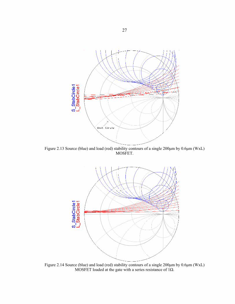
shown in Figure 2.13 was obtained by simulating the S-parameters of a single 200μm by
0.6μm (WxL) device in a 50Ω system from 0.5-5GHz in 0.5GHz steps. Both S11 and S22
were found to be less than one throughout this frequency range. Note that while the
center of the Smith chart is a region of stability, above 50Ω there exists real impedances
for which the system may exhibit instability. In order to judge the potentiality for an
unstable system the gate of the transistor was loaded with a marginal series resistance
(1Ω). The result of this simulation can be seen in Figure 2.14. Loading the gate of this
transistor with a series resistance of ~1Ω or greater would thus ensure that the device is
stable for all real impedances. As will be seen in the following chapter this criteria is met
through the loading presented by the realized transmission lines.
11 22 12 21.S S S S∆ = −
27
Figure 2.13 Source (blue) and load (red) stability contours of a single 200μm by 0.6μm (WxL) MOSFET.
Figure 2.14 Source (blue) and load (red) stability contours of a single 200μm by 0.6μm (WxL) MOSFET loaded at the gate with a series resistance of 1Ω.

28
Once a transistor size and bias operating point is decided upon the design of the
transmission lines can be undertaken using expressions 2.6 and 2.10 and the phase
velocity equalization requirement addressed in expression 2.14. The focus of the
subsequent chapter will be upon this design process.

29
CHAPTER 3
CMOS TRANSMISSION LINE REALIZATION
Transmission Line Parameters
Recall that the lumped-element equivalent circuit of a section of loaded
transmission line is comprised of four primary parameters (the series resistance REQ, the
series inductance LEQ, the shunt conductance GEQ, and the shunt capacitance CEQ,)
encompassing the per unit length parameters of the TL itself and the “absorbed”
parasitics of the loading transistors (Figure 2.7). Using this equivalent circuit the
expressions for the characteristic impedances of the gate and drain lines were shown in
the previous chapter to be
(3.1)
and
(3.2)
respectively. Knowing the transistor parasitic values and defining a design criteria for the
system impedance allows one to realize the required unloaded TL parameters. The DC
parasitic capacitances of the 200μm x 0.6μm (WxL) NMOS transistor obtained through
SPICE simulation (and the subsequent calculation values of the Miller capacitance) are
tabulated in Table 3.1.
' ,( / )
g gg
g g gs g
R j LZZY G j C C l
+ ω= =
+ ω +
',
1 ( / )d d
d
d d M do d
R j LZZY G j C C l
r l
+ ω= =+ + ω +

30
Parameter Value UnitGate/Drain overlap capacitance, Cgdo 6.0x10⁻¹⁴ FGate/Source overlap capacitance, Cgso 6.0x10⁻¹⁴ FGate/Bulk capacitance, Cgb 1.185x10⁻¹⁴ FGate/Drain capacitance, Cgd 1.03x10⁻¹⁴ FGate/Source capacitance, Cgs 2.683x10⁻¹³ F
Drain current, ID 66 mATransconductance, gm 75 mSMiller capacitance (Gate), CM 1.698x10⁻¹³ FMiller capacitance (drain), CM' 9.278x10⁻¹⁴ F
Table 3.1 DC parasitic parameter values of a 200μm x 0.6μm (WxL) NMOS transistor.
Coplanar Strip-line (CPS) Selection and Design
The choice of transmission line realization in CMOS technologies requires that
the TL be able to be fabricated using the available photolithographic processes. This
limitation typically restricts one's choice to those realizable via planar two-conductor
geometries. Microstrip and coplanar waveguide (CPW) are two such geometries. The
choice between these two geometries rests in the application desired. Microstrip lines
demonstrate an advantage over CPW lines in that the ground plane provides intrinsic
shielding from the lossy substrate (see Figure 3.1), lessening line losses due to capacitive
substrate coupling.

31
Figure 3.1 Microstrip transmission line realized in CMOS substrate using the highest (yellow) and lowest (red) metal interconnect layers.
In the same manner, the ground plane also provides the microstrip line designer
with a measure of insensitivity to the processing done previous to the ground plane
creation. These advantages aside however, microstrip is most often not the most suitable
choice of transmission line structure in distributed CMOS designs. In the 3-metal CMOS
process used in the DA design of this project the separation between the lowest metal
layer (Metal 1) and the highest metal layer (Metal 3) is approximately 1.56μm (see
substrate diagram in Figure 3.2).
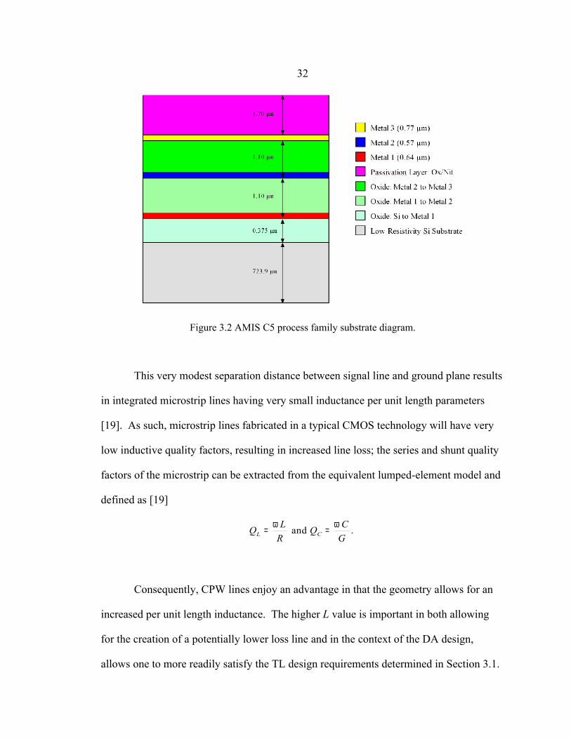
32
Figure 3.2 AMIS C5 process family substrate diagram.
This very modest separation distance between signal line and ground plane results
in integrated microstrip lines having very small inductance per unit length parameters
[19]. As such, microstrip lines fabricated in a typical CMOS technology will have very
low inductive quality factors, resulting in increased line loss; the series and shunt quality
factors of the microstrip can be extracted from the equivalent lumped-element model and
defined as [19]
Consequently, CPW lines enjoy an advantage in that the geometry allows for an
increased per unit length inductance. The higher L value is important in both allowing
for the creation of a potentially lower loss line and in the context of the DA design,
allows one to more readily satisfy the TL design requirements determined in Section 3.1.
and .L CL CQ Q
R Gω ω= =

33
One disadvantage to CPW lines is that the geometry requires two adjacent ground
lines, see Figure 3.3, and thus can consume substantial amounts of die real estate. To
avoid this costly consumption of die area the single adjacent ground line equivalent,
coplanar stripline (CPS), can be chosen. CPS also enjoys the benefit of being able to
attain higher characteristic impedances than that of CPW with equal resistive losses (e.g.
using larger line widths) [20]. As mentioned in Chapter 2, the realization of high
characteristic impedance TLs with tight tolerances can be difficult to realize in a
commercial IC process technology due to fabrication process variation and intrinsic
substrate variables such substrate resistance.
Figure 3.3 Coplanar waveguide cross-sectional illustration.
The design of the CPSs includes the selection of the line widths and spacing given
the process parameters for the metal trace used and the resulting substrate; see Figure 3.4.
This can be accomplished through the various analytical formulas developed for the
analysis of coupled microstrip lines [21-23] and those specifically developed for the
analysis of CPS [24-25]. The LineCalc program contained within the ADS suite uses
those formulas developed by [22] and [23] to allow the user to quickly obtain electrical

34
and physical parameters of the coupled transmission lines of CPS geometries at specific
frequencies of interest. The user supplies the program with the necessary substrate
(effective dielectric constant Er, permeability Mur, and thickness H) and conductor
(thickness T and conductivity Cond) parameters and selects a desired characteristic
impedance for a selected design frequency and is returned the appropriate line widths and
spacing.
Figure 3.4 Coplanar stripline cross-sectional illustration.
The structural parameters used were obtained from the C5 process technology
design rules and are shown graphically in Figure 3.2. In order to minimize the coupling
effects between the CPS and the low-resistivity silicon substrate the top metal layer
(Metal 3) was chosen for the implementation of the transmission lines. The process
specifications as obtained from the design rules for this metal layer are given in Table
3.2. Note that the metal conductivity is found by simply dividing the sheet resistance RS
by the metal thickness t.

35
Parameter Min Typ Max UnitThickness, t 7000 7700 8400 ÅSheet Resistance, RS 33 40 47 m-
ohms/sq
Electromigration (10yr life
expectancy)
85 ˚C 125 ˚C
Allowed current density per width 2.2 mA/μm 0.85 mA/μm
Table 3.2 AMIS C5 process specifications for metal layer 3.
In order to determine the effective dielectric constant of the silicon substrate,
silicon dioxide combination the method-of-moments (MoM) based electromagnetic (EM)
simulator IE3D [26] was utilized in modeling the substrate shown in Figure 3.2 (minus
the passivation layer). A simulation of an arbitrary uniform 2-port transmission line
structure upon this substrate allowed the complex effective dielectric constant to be
extracted versus frequency for use within LineCalc. An exact solution (W=48μm,
S=4μm) for a 50Ω CPS implemented in the C5 process at a frequency of 1GHz was then
deduced using the LineCalc program and constructed in IE3D for EM simulation. This
frequency was chosen so as to minimize the error induced in the IE3D extraction of the
RLGC parameters while still being high enough to maintain a reasonable idea of the
high-frequency characteristics of the TL3. As such, using the RLGC extraction tool
within IE3D, the lumped-element equivalent parameters were extracted for the CPS at
1GHz and can be seen in Table 3.3; see Appendix D for a complete extraction to 15 GHz.
3 IE3D uses an “Error Factor” term to give the user an indication of the relative error of an RLGC equivalent approximation for a segment of transmission line. This error factor (E) is defined to be equal to the square-root of the absolute value of the input impedance of the lumped-element circuit when the output is shorted over the input impedance with an open output. The relative error in an extraction can then be computed by the expression: 1 – sqrt(1 – E2)*100%.

36
Parameter Value UnitFrequency 1.000 GHzSeries R 0.99382 OhmsSeries L 0.27849 nHShunt R 6371.6 OhmsShunt C 0.11788 pF
Table 3.3 IE3D extracted RLGC parameters for a 500μm, 50Ω CPS.
The calculation of the characteristic impedance of this TL at 1GHz is thus given,
where
Upon obtaining the RLGC values for the 50Ω CPS, the device parasitics were
obtained through simulation at a frequency of 1GHz (Table 3.4) and applied to equations
3.1 and 3.2 in order to observe the loading effects upon the TL characteristic impedances.
By inspection, one can see that the net effect of the device loading is to significantly
lower the characteristic impedances of the gate and drain lines. Hence, the subsequent
step is to increase the unloaded CPS characteristic impedances to the point at which the
loaded lines would have a characteristic impedance of 50Ω. Observe from the data in
Table 3.4 that the gate line must be designed to account for a larger loading capacitance
than the drain line. This requires that the series resistance and/or series inductance of the
0 51.555 .Z = Ω
00.99382 2 (1 9)(2.7849 10) (50.946 7.901) ,
1 2 (1 9)(1.1788 13)6371.6
j e eZ jj e e
+ π −= = − Ω+ π −

37
gate line be greater, leading to a potential disparity in both attenuation and phase velocity
between the two lines.
Parameter Value UnitGate Capacitance 3.39x10⁻¹³ FDrain Capacitance 3.22x10⁻¹³ F
Drain current, ID 66 mATransconductance, gm 75 mS
Table 3.4 Parasitic parameter values of a 200μm x 0.6μm (WxL) NMOS transistor at 1GHz.
Through an iterative process of selecting new width and spacing values for increasing
values of characteristic impedances using LineCalc, extracting the RLGC parameters via
full-wave EM simulation in IE3D, and applying equations (3.1) and (3.2), device loaded
50Ω CPS were created for both the gate and drain lines. The width, spacing, and
unloaded characteristic impedance of the gate and drain lines are given in Table 3.5 along
with the extracted RLGC parameters for the two lines. Note that while (3.1) and (3.2)
would seem to simply imply that increasing the series inductance is sufficient to equalize
the impedances of the gate and drain TLs at 50Ω, it was discovered that increasing the
spacing alone did not sufficiently increase the impedance of the respective lines and thus
the widths of the TLs were also decreased. This departure from the predicted is attributed
to substrate dependence not accounted for in (3.1) and (3.2).

38
Parameter Value Unit- Gate Drain -
Width 7.0 10.0 μmSpacing 12.0 10.0 μmZO 140.823 116.171 ΩFrequency 1.000 1.000 GHzSeries R 5.7324 4.0289 ΩSeries L 0.50907 0.44292 nHShunt R 1.1102e5 71303 ΩShunt C 0.026784 0.03431 pF
Table 3.5 IE3D extracted RLGC parameters for 500μm gate and drain CPS.
Including the parasitic capacitances from Table 3.4 into the RLGC extracted
parameters in Table 3.5 yields a calculated complex gate line impedance of
where
and a complex drain line impedance of
( ) ( )( )5.7324 2 (1 9)(5.0907 10) (46.076 26.933) ,
1 2 (1 9) 2.6784 14 3.40 131.1102 5
gj e eZ j
j e e ee
+ π −= = − Ω+ π − + −
53.37 ,gZ = Ω
( ) ( )( )4.0289 2 (1 9)(4.4292 10) (41.482 21.597) ,
1 2 (1 9) 3.431 14 3.22 1371303
dj e eZ j
j e e e
+ π −= = − Ω+ π − + −

39
where
After determining the appropriate geometries for the respective lines, the disparity
in phase velocities between the two was then addressed. The phase velocity of a signal
traveling upon a TL can be expressed as [13]
(3.3)
Combining (3.3) with the expression for the characteristic impedance of a lossless TL,
(3.4)
allows ones to obtain expressions for the phase velocities upon both the gate,
(3.5)
and drain lines,
(3.6)
Observing (3.5) and (3.6) allows to to note that the larger series inductance of the
gate line Lg introduces additional phase delay, thus making it necessary to increase the
1 .pvL C
=⋅
0 ,LZC
=
0 ,GATEp
G
ZvL
=
46.77 .dZ = Ω
0 .DRAINp
D
ZvL
=

40
delay incurred in the drain line by an equal amount. This can be easily accomplish by
increasing the length ld of the drain line sufficiently to satisfy the relationship
(3.7)
Satisfying this relationship results in a drain line length of 575μm. In order to facilitate
layout the drain line was designed to occupy the same horizontal distance (500μm) as the
gate line by including two jogged sections in the drain line. A micrograph of the gate and
drain lines can be seen in Figure 3.5.
Figure 3.5 Micrograph of the fabricated gate and drain CPS.
.g d
d g
L lL l
=

41
Optimal Device Quantity Deduction
Once the characteristics of the gate and drain TLs are known, it is then possible to
derive the optimal number of stages the DA should be designed for using (2.20). The
electromagnetic simulator IE3D was used to extract the attenuation factors of each line.
Knowing these, along with the intermediary lengths, allowed (2.20) to be used to find the
optimal number of stages as follows:
An optimal stage number of two is thus arrived at for a starting design point.
Following this determination the DA design was simulated in ADS using the appropriate
models. The transistors were modeled using the provided BSIM3v3 models, while the
transmission line structures were modeled using the method-of-moments based
electromagnetic simulator present within ADS entitled Momentum. It was discovered
during these simulations that in fact six stages could be implemented before the
attenuation in the TLs overcame the gain improvements resulting from the addition of
active devices. A 50Ω system consisting of six CPS delay line connected 200μm by
0.6μm (WxL) multi-fingered MOSFET transistors was thus decided upon as the final DA
design configuration. At this point in the design each device was optimally biased by
individual RF-choked voltages sources. The subsequent chapter will address feasible
means of biasing these devices on-chip via an external voltage source.
( )
( )
( ) ( )
10.9161 500μmmmln
10.92262 575μmln( / ) mm( ) 2.03.
1 10.9161 500μm 0.92262 575μmmm mm
g g d dMAX
g g d d
l lM G
l l
α α = = =α − α −

42
CHAPTER 4
BIASING AND PLANAR INDUCTOR DESIGN
Distributed Amplifier Biasing
In order to realize a fully integrated distributed amplifier the bias network must
necessarily be realized on chip as well. Previous implementations of distributed
amplifiers in conventional CMOS technologies have relied upon bias-T [27-28] and
package parasitics [29] to implement the requisite RF blocking mechanisms within the
DA design. A primary focus of the DA design of this thesis was the implementation of a
monolithic DA circuit topology. In addition, this work was carried out with the goal of
realizing a DA sub-circuit that could be readily utilized within a larger 50Ω RF system
design. Consequently, a biasing scheme for the six transistors comprising the amplifiers
within the design was created to allow for simple system integration with minimal
complexity power supply requirements.
The biasing method decided upon utilizes four square-spiral inductors (the
selection and design of which is discussed in the subsequent section) acting as RF-chokes
in the configuration shown in Figure 4.1. This configuration was chosen through a trial-
and-error process starting from an optimal configuration in which RF-chokes were placed
so that each device was provided immediate bias connections to the positive and negative
power supply voltages as shown in Figure 4.2.
This implementation of the bias network was chosen over an implementation of
the widely used analog building block, the current mirror, in order to achieve a bias
network with the broadest frequency response in terms of device loading and
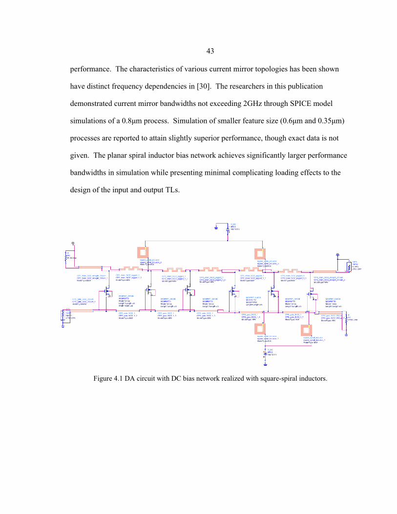
43
performance. The characteristics of various current mirror topologies has been shown
have distinct frequency dependencies in [30]. The researchers in this publication
demonstrated current mirror bandwidths not exceeding 2GHz through SPICE model
simulations of a 0.8μm process. Simulation of smaller feature size (0.6μm and 0.35μm)
processes are reported to attain slightly superior performance, though exact data is not
given. The planar spiral inductor bias network achieves significantly larger performance
bandwidths in simulation while presenting minimal complicating loading effects to the
design of the input and output TLs.
Figure 4.1 DA circuit with DC bias network realized with square-spiral inductors.

44
Figure 4.2 ADS schematic of DA circuit with an optimal DC bias network realized with ideal RF-chokes.
From this initial configuration, the loading effects of the square-spiral inductors
were examined in order to determine the effects upon circuit performance. Initially it
was believed that the bias inductors could easily be incorporated into the transmission
line design, however, through simulation it was found that the imperfect RF-choke nature
proved a greater detriment to the performance of the DA than the added inductive loading
effects. The initial bias network provided an alternate route for the RF-signal resulting in
considerable signal attenuation upon both the gate and drain lines. However, limiting the
bias connections to single locations upon the respective transmission lines proved
inadequate in terms of device biasing. Therefore it was determined through simulation
that a pair of the designed square-spiral inductors provided a suitable balance between
signal degradation and bias voltage levels experienced by each device. The attenuation
experienced upon the lines also severely affected the supplied DC voltage level. From
RF-input to the gate of the sixth transistor a 0.63V drop in DC potential was predicted

45
upon the gate line through ADS simulation when using a bias-T setup and 2.5V power
supply voltages. Similarly, a 1.21V drop in voltage level on the drain line was simulated.
Thus, the topology shown in Figure 4.1 was chosen as a comprise between the signal
attenuation experienced and the DC voltage level supplied to each device. The actual
design of the spiral inductors and simulated characteristics are discussed in the
subsequent section.
Planar Spiral Inductor Design
Inductor implementations in commercial integrated circuit technologies are
practically limited to either bond wires or planar spiral geometries. Bond wires typically
provide higher Q values, typically an order of magnitude, and less resistive loss than
planar spiral inductors but are typically limited in their inductance values by the bonding
process and tend to not lend themselves to a well controlled inductance value [31].
Consequently, planar spiral inductors are customarily chosen for their well-defined
inductance properties at the sacrifice of a limited Q-factor. For the reasons discussed in
Section 4.1 the self-evident choice of inductor implementation was that of the planar
spiral geometry type. The exact choice of polygonal layout is up to the designer and can
range from the most simple square spiral, Figure 4.3a, to the wholly circular spiral,
Figure 4.3d. Increasing the number of polygonal sides typically results in a higher Q
inductor at the cost of a slightly decreased inductance value for the same design
dimensions.
The planar inductors discussed forthwith are implemented using solely the top
metal layer (M3). The reasons for this choice include a desire to minimize the coupling

46
effects between the inductor and the lossy silicon substrate and additionally, to minimize
the power lost within trace. The latter reflects the process decision to relegate the top
metal layer for such purposes as power routing and passive element realization. While
multilayer realizations of planar spiral inductors demonstrating reduced areas for
comparable inductance values can be found in literature [32-33], these designs typically
employ more advanced processes which enjoy the advantage realized through the reverse
thickness scaling of the CMOS interconnect stack (increased separation distance between
interconnect layers and the silicon substrate resulting in reduced capacitive coupling
effects). In addition, the conductivity of the initial and secondary metal interconnect
layers within the AMIS C5 process are approximately half that of the third layer. This
additional loss, in conjunction with the small interconnect stack distances, makes the
creation of a high Q-factor multilayer inductor in the AMIS C5 a problem beyond the
scope of this project.

47
Figure 4.3 Planar spiral inductor geometries for (a) square, (b) hexagonal, (c) octagonal, and (d) circular realizations [31].
Inductor Figures of Merit
Passive inductor design includes several important FOM in realizing the inductor
with the required properties. Foremost among these is of course the inductance itself.
The most accurate method of obtaining the inductance is through the use of a three-
dimensional (3-D) EM simulator such as [34]. Due to the significant computational run
time required for such a simulation however, this approach is more useful as a
characteristic validation step than as an initial design step. The use of approximate
analytical expressions is thus the most desirable method for determining the geometry
necessary to realize the required inductance value. Presented in [31] are three simple,

48
approximate expressions of planar spiral inductors of square, hexagonal, octagonal, and
circular geometries. These expressions fully characterize the inductance of these
geometries given the number of turns n, the line width w, the line spacing s, the average
diameter davg ( 0.5·(dout + din) ) and the fill ratio ρ ( (dout - din)/(dout + din) ). The fill ratio is
an indicator of how hollow the center of the spiral is. This is important in that an
inductor with a fuller center will have a smaller inductance than one with a larger center
spacing even while the two have the same average diameter due to the increased negative
mutual inductance of the tighter inner turns of the first. One should also note that while
these inner turns contribute less inductance they contribute no less series resistance,
making it doubly important that a sufficiently large fill factor is maintained. A rule of
thumb for a desirable fill factor value is approximately 0.5 [35]. Two of the expressions
from [31] were selected for utilization in the analytical design of the required planar
spiral inductors and will be discussed here.
The first, referred to as the modified Wheeler expression, takes the form
(4.1)
where K1 and K2 are the polygon dependent coefficients given in Table 4.1 and μ0 is the
permeability constant (4π x 10-7 [H/m]) [31].
2
1 02
,1
avgmw
n dL K
K= µ
+ ρ

49
Polygon K1 K2Square 2.34 2.75
Hexagonal 2.33 3.82Octagonal 2.25 3.55
Table 4.1 Coefficients for modified Wheeler expression [31].
The second expression given by [31] is based on an approximation of the spirals as
symmetrical current sheets of equivalent current densities and is shown to be given by
(4.2)
where the coefficients ci are again polygon dependent; see Table 4.2.
Polygon c1 c2 c3 c4Square 1.27 2.07 0.18 0.13
Hexagonal 1.09 2.23 0.00 0.17Octagonal 1.07 2.29 0.00 0.19
Circle 1.00 2.46 0.00 0.20
Table 4.2 Coefficients for current sheet expression [31].
Both approximations were shown to exhibit agreement with field solver inductance
values and within ~3% and within ~5% for actual measured results by [31].
A second important FOM for planar spiral inductors is the series resistance of the
inductor. The series resistance calculation of an planar spiral inductor realized in a
typical CMOS technologies must account for losses incurred by the capacitive coupling
of the metal layer to the substrate in the form of eddy current, in addition to the typical
( )2
0 1 22 3 4ln( / ) ,
2avg
gmd
n d cL c c c
µ= ρ + ρ + ρ

50
wire calculations accounting for the finite conductivity of the metal and its frequency
dependent skin depth. As such the total series resistance can be approximated by the
expression
(4.3)
where the first term accounts for the finite metal conductivity and skin depth effects and
the second term accounts for the induced eddy current losses [35]. The individual
variables are defined as follows: w is the metal width, σ is the metal conductivity, l is the
total length of the winding, t is the metal thickness, δ is the skin depth given by
(4.4)
σsub is the substrate conductivity, e is the real number constant equal to 2.7182..., and zn,ins
and zn,sub are the total thickness of the insulation between the metal layer and the
conductive substrate and the substrate skin depth (both normalized to davg), respectively
[35].
Once the series inductance and resistance are computed a first-order
approximation of the inductor's Q-factor can be made by using the quality factor
definition to relate the energy stored per cycle to the energy lost per cycle. This
relationship can be expressed simply as
( ) ( ) 2 3 0.7 0.55 0.1, ,/
,41
subS avg n ins n subt
lR n f d z zew e
−− δ
σ= + µ ⋅ ⋅ ρ⋅ σ ⋅ δ −
0
2 ,δ =ω ⋅ µ ⋅ σ

51
(4.5)
where LS is the series inductance predicted by (4.1) or (4.2) and RS is the series resistance
approximated by (4.3).
The final FOM significant to the implementation of a suitable RF-choke is the
inductor's frequency of self-resonance (SRF). This frequency is defined to be the point at
which the inductor's Q value is equal to zero. At frequencies beyond this point the
inductor takes on an impedance that is capacitive in nature eventually negating its
usefulness as an RF-choke. Consequently, the inductor must be designed such that its
SRF is sufficiently high as to not inhibit the broadband capabilities of the DA itself. This
requirement in and of itself is not a trivial matter and is further complicated by the
increased capacitive losses due to the low-resistivity substrate. However, due to the low
Q-factors ( < 2) of the planar spiral inductors realizable in the process used, the SRF did
not need to be placed at the upper end of the DA's expected bandwidth.
In considering the implementation of a planar spiral inductor to serve as a suitable
RF-choke in regards to the design of a broadband DA the three FOM visited above are
weighed in order to achieve an inductor that simultaneously achieves a sufficiently high
SRF, an inductance value large enough to mitigate the propagation of phase-incoherent
RF signals through the bias network, and a minimal DC series resistance.
Planar Spiral Inductor Implementation
The limitations of the Cadence suite [36] used in this project restricts the
geometry of any structure to one with 45º turns, thus limiting the polygon choice to
,SL
S
LQR
ω=

52
hexagonal or square. In order to facilitate rapid design iterations a square topology was
chosen. In addition, a maximum outer diameter of 450μm was decided upon in order to
ensure that the final die cost did not exceed ~5000USD4. With this restriction in mind
the computer algebra system distributed by Mathsoft entitled Mathcad was used to
simultaneously implement equations (4.1), (4.2), (4.3) and (4.5) in order to determine the
dimensions of a square spiral inductor that achieved the greatest inductance value
possible while maintaining an SRF near 5GHz. These constraints led to the
determination of an inductor with the following dimensions: dout = 447.7μm, din =
213.3μm, w = 24.5μm, s = 2.0μm, and n = 4.25 (see Appendix E for Mathcad derived
plots used to graphically weigh the dimensional constraints against the desired inductance
values). Momentum was then used to model the inductor and obtain the following
important inductor FOM via the S-parameters: an inductance value of ~10nH, a DC
series resistance of ~9.8Ω, and a SRF of ~4.5Ghz.
4 MOSIS MEP Research Account price for the 0.5μm AMIS C5 process listed at $650*(die size in mm2), http://www.mosis.org/orders/prices/mep/.

53
CHAPTER 5
CALIBRATION AND CHARACTERIZATION
Introduction
As previously mentioned this work was carried out with the goal of realizing a
DA sub-circuit that could be readily utilized within a larger RF system design. To that
end, the parts fabricated were designed to enable a probed response to be easily acquired
and used to characterize the operation of the DA device, the sub-circuits, and all
associated passive elements. All measurements were conducted in the on-wafer high-
frequency test facility housed in the Microwave and mm-Wave Electronics Laboratory at
Montana State University – Bozeman. This facility is home to a Cascade Microtech
Microchamber Probe Station and a N5250A mm-wave vector network analyzer (VNA)
from Agilent Technologies. Available for on-wafer probing at the facility are four DC
positioners (and associated probes) from Cascade Microtech and three model 40A CPS
RF Picoprobes from GGB Industries Incorporated. The footprint of the available RF
probes is an important factor that must be considered during the layout of all components
to be probed. A diagram of the tip configuration of the laboratory's probes is shown in
Figure 5.1. The probes are of a ground-signal (GS) and signal-ground (SG) configuration
with a pitch (tip separation) of 50μm.

54
Figure 5.1 GGB model 40A CPS RF probe tip diagram.
Calibration
The first task to be completed during a measurement is that of calibration.
Calibration is the procedure of removing sources of measurement error, at least to the
extent possible. Calibration is separated into two types, response calibration and vector
calibration [37]. Response calibration is limited to the correction of scalar errors, while
vector calibration corrects for both magnitude and phase errors. When performing any
type of device measurement there will be sources of error present that will affect the
measurement data obtained. This measurement error can be grouped into three general
types of error: drift, random, and systematic [37]. Drift error is caused by system
variations over time that occurs after a calibration has been completed. This type of error
is both time and temperature dependent and depends heavily on the robustness of the test
system present. Minimizing drift error is accomplished by maintaining both a constant
test environment and regular system validation procedures as prescribed by the device
manufacturer. A simple but important task in this regard is to incorporate a warm-up

55
period for active test equipment into the calibration procedures in order to allow the
equipment to reach thermal equilibrium. Random errors are by definition those that are
completely unpredictable by nature and cannot be removed through calibration. The
operator typically has no control of this type of error, as it chiefly depends upon the noise
present within the test instruments themselves. Finally, systematic errors are those due to
imperfections in the test instruments and test setups that are repeatable and time-
invariant. Consequently, the contribution of systematic errors are readily characterized
and used to create equivalent error boxes. During measurements of the device-under-test
(DUT) these error boxes can then be used to mathematically remove the systematic error
contributions.
The systematic error boxes are determined by measuring known calibration
standards. A specific calibration kit (cal-kit) consisting of the set of known standards is
used for this purpose. These standards typically involve some combination of reflects
(opens and shorts), terminations, and thrus. Perfect opens and shorts reflect 100% of the
incoming waves, ideal terminations absorb 100% of the incident waves, and error-less
thrus fully transmit the signal with no attenuation or phase change. The disparities of the
standards within the cal-kit to that of perfect standards are characterized and stored as
calibration coefficients within the cal-kit definition file. The calibration coefficient
definition file stored within the VNA is then used in conjunction with the standard
measurements to form the 6-term (directivity, source match, load match, reflection
tracking, transmission tracking, and crosstalk) reflection and transmission error boxes
[37]. Thus, a full 2-port calibration requires a 12-term error correction model.
The type of calibration standards to be used defines the mathematical derivation

56
actually performed in order to arrive at these error boxes. Different derivation methods
and the associated impedance standards make up the various calibration techniques
existent in device characterization and measurement today. During the course of the
measurements carried out in this work the two most common (SOLT and TRL)
calibration techniques were effected.
Short-Open-Load-Thru (SOLT)
In a SOLT calibration there are four known reference standards, a short, an open,
a load, and a thru. The accuracy of these standards directly correlates to the accuracy of a
SOLT calibration, the more precise the standards, the more accurately the systematic
errors can be defined [38]. This direct dependency upon the accuracy of the standards
proves the SOLT method's greatest liability. It is often difficult to build easily defined
calibration standards in the variety of TLs used today, with the problem becoming
increasingly difficult to maintain at higher frequencies. For example, in CPS
measurements the opens will radiate energy and the shorts will have an measurable
inductance associated with them.
During this work a SOLT calibration was performed from 10MHz to 5GHz using
a GGB calibration substrate (CS-8). This calibration placed the reference plane at the
probe tips and does not de-embed any of the on-chip parasitics. To assess the quality of
the calibration both a thru standard and a short standard were measured after calibration.
Figure 5.2 shows a representative set of S-parameters of a 400μm thru line from the CS-8
calibration substrate after calibration. Return loss of better than 60dB is seen throughout
virtually the entire frequency range (10MHz – 5GHz), suggesting an excellent
calibration.

57
Figure 5.2 Measured 2-port S-parameters of a CS-8 thru line after SOLT calibration.
Similarly, Figure 5.3 shows the reflection from a short circuit on the CS-8
calibration substrate after the SOLT calibration upon a Smith chart. The frequency range
shown in Figure 5.3 is 10MHz to 1GHz. From this figure it is again clear that the error
correction model arrived at from SOLT calibration is in excellent agreement in terms of
both magnitude and phase.

58
Figure 5.3 Measured reflection from a CS-8 short circuit after SOLT calibration.
Thru-Reflect-Line (TRL)
In order to circumvent the shortcomings of the SOLT calibration techniques,
several methods have been developed requiring reduced numbers of well-defined
standards. The TRL calibration method is perhaps the most popular alternative. This
technique relies on the use of multiple transmission lines in place of the discrete
impedance standards [39]. It requires only three simple standards, a short section of TL
to connect ports 1 and 2 (the thru), identical high-reflection opens or shorts (the reflects)
for both ports, and a second longer section of TL to connect ports 1 and 2 (the line). As
such an immediate advantage of the TRL method lines in the relative ease of designing
the required cal-kit. Also, only the first standard, the thru, need be precisely-defined for
an accurate derivation of the 12-term error correction model using the TRL calibration

59
technique [38]. Consequently, the characteristic impedance of the thru line must be
designed for that of the device to be measured in order to avoid measurement error.
In addition the optimal electrical length of the thru line is said to be 90° at the
center frequency of bandwidth over which the device is desired to be characterized [38].
The length of the line is optimally defined to 90° greater than that of the thru at the center
frequency, with a typical useful frequency range of 20° to 160° [38]. The bandwidth of a
TRL calibration is thus limited by the line standard used. Larger bandwidth require the
use of additional line standards. The required line length likewise restricts the usefulness
of the TRL calibration technique to the higher RF frequencies as the length becomes
prohibitively large at lower frequencies.
On-chip calibration standards were designed and fabricated on the DA die to
facilitate a TRL calibration to the probe tips. The standards designed included 50Ω thru
CPS of length 500μm, open and short reflects terminating 250μm CPS, and a 4686μm
CPS line (see Figure 5.4). This TRL calibration places the reference plane at the center
of the thru line, thus making it an ideal method in which to de-embed TL effects right up
to the DUT.

60
Figure 5.4 Micrograph of the fabricated CPS TRL calibration standards; TOP-open reflects, MIDDLE-short reflects, BOTTOM-thru line.
The guided wavelength of the 50Ω thru line is given by,
(5.1)
where the effective dielectric constant (εeff) of 5.57 was estimated from IE3D simulation
of the transmission line. The optimal line length was previously mentioned to be equal to
90º (λ/4) greater than the length of the thru line at the center frequency. Given the
fabricated line lengths of 500μm and 4686μm the center frequency of this TRL cal-kit is
calculated to be
83 10 [ / ] ,5.57g
eff
c m sf f
×λ = =ε

61
(5.2)
Using the rule of thumb from [38] the range of acceptable calibration performance
around this frequency is calculated as follows
(5.3)
(5.4)
where the acceptable TRL calibration bandwidth is calculated as
However using the program FINDLEN offered by the NIST5, it was found the maximum
standard deviation for this frequency range is equal to ~2.91. In personal communication
with Dr. Dylan Williams of NIST it was recommended that this range be reduced until a
max standard deviation of ~1.0 was achieved. With the available line standards and a
complex εeff equal to 4.785659 – j2.822164 at 7.6GHz it was found that a minimum max
standard deviation of 1.10 resulted from a frequency range of 6.75GHz – 8.25GHz. This
is significantly tighter than former acceptable bandwidth.
A TRL calibration was performed over this bandwidth using the iterative
calibration algorithm [40] implemented in the software package StatistiCALTM (see
5 National Institute of Standards and Technology, Electronics and Electrical Engineering Laboratory, Radio-Frequency Electronics Group (http://www.boulder.nist.gov/div818/81801/dylan/software.html).
8
/41 1 3 10 [ / ] 7.6GHz.4 4( ) (4686 m 500 m) 5.57g
line thru eff
c m sfl lλ
×= = =− ε µ − µ
4 /9 /18BW = - = 13.5GHz - 1.7GHz = 11.8 GHz.g g
f fλ λ
8
/181 1 3 10 [ / ] 1.7GHz,
18 18( ) (4686 m 500 m) 5.57gline thru eff
c m sfl lλ
×= = =− ε µ − µ
8
4 /94 4 3 10 [ / ] 13.5GHz,9 9( ) (4686 m 500 m) 5.57g
line thru eff
c m sfl lλ
×= = =− ε µ − µ
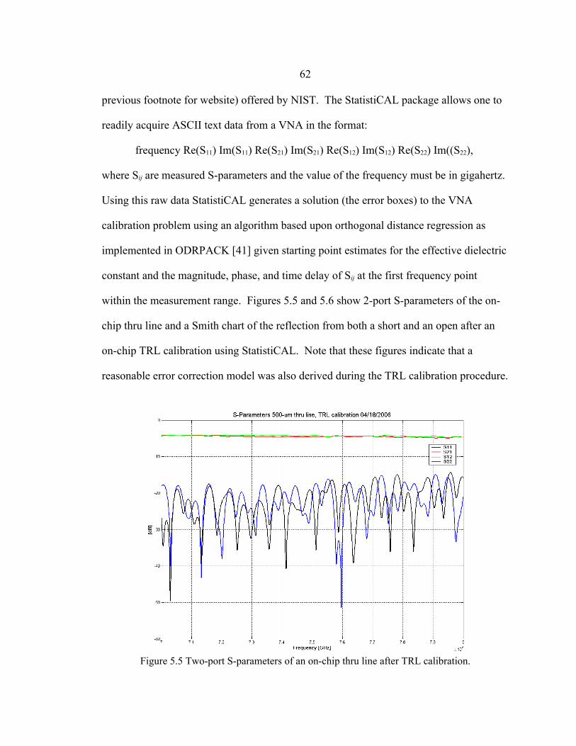
62
previous footnote for website) offered by NIST. The StatistiCAL package allows one to
readily acquire ASCII text data from a VNA in the format:
frequency Re(S11) Im(S11) Re(S21) Im(S21) Re(S12) Im(S12) Re(S22) Im((S22),
where Sij are measured S-parameters and the value of the frequency must be in gigahertz.
Using this raw data StatistiCAL generates a solution (the error boxes) to the VNA
calibration problem using an algorithm based upon orthogonal distance regression as
implemented in ODRPACK [41] given starting point estimates for the effective dielectric
constant and the magnitude, phase, and time delay of Sij at the first frequency point
within the measurement range. Figures 5.5 and 5.6 show 2-port S-parameters of the on-
chip thru line and a Smith chart of the reflection from both a short and an open after an
on-chip TRL calibration using StatistiCAL. Note that these figures indicate that a
reasonable error correction model was also derived during the TRL calibration procedure.
Figure 5.5 Two-port S-parameters of an on-chip thru line after TRL calibration.

63
Figure 5.6 Input impedances of on-chip short and open reflects after TRL calibration.
Measurements
Delay Line Validation
In order to ensure that the phase velocities of the fabricated gate and drain lines
corresponded to that of the electromagnetic simulated models, isolated sections of each
were fabricated and probed after an SOLT calibration (see Figure 5.7). The simulated
phase delay difference between the drain delay line and the gate line was predicted to
vary from nearly 0º at 10MHz to approximately 1.7º at 5GHz (see simulation schematic
and results shown in Figures 5.8 and 5.9, respectively).

64
Figure 5.7 Micrograph of an isolated drain delay line being probed after SOLT calibration.
Figure 5.8 ADS delay line phase difference simulation schematic.

65
Figure 5.9 Delay line phase difference, ADS simulation.
The probed response suggested that the actual phase delay difference vary
relatively linearly from approximately 0º at 10MHz to full degree greater than simulated,
or approximately 2.7º, at 5GHz, as is shown in Figure 5.10. While the impact of this
deviation is difficult to assess in terms of the loaded transmission lines it is concluded
that this error is a comparatively small contributor to the total DA performance variance
(in terms of simulated versus measured) seen.
1 2 3 40 5
0.5
1.0
1.5
0.0
2.0
freq, GHz
ph
ase
(S(2
,1))
-ph
ase
(S(4
,3))
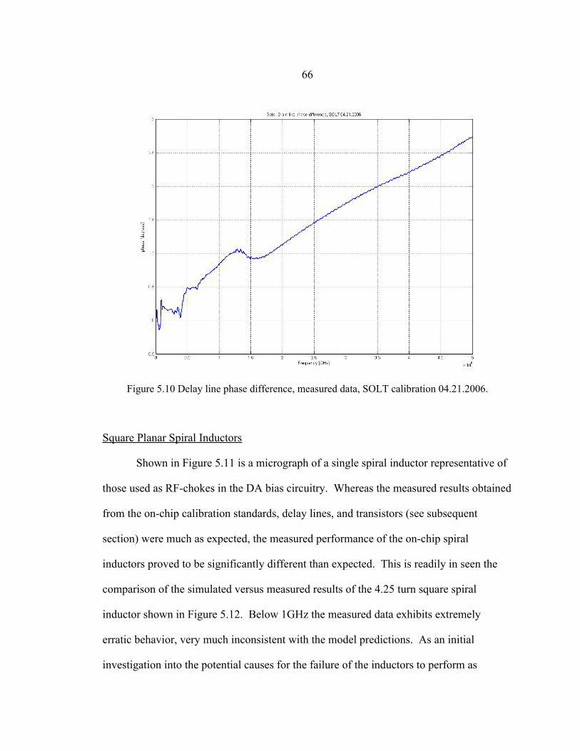
66
Figure 5.10 Delay line phase difference, measured data, SOLT calibration 04.21.2006.
Square Planar Spiral Inductors
Shown in Figure 5.11 is a micrograph of a single spiral inductor representative of
those used as RF-chokes in the DA bias circuitry. Whereas the measured results obtained
from the on-chip calibration standards, delay lines, and transistors (see subsequent
section) were much as expected, the measured performance of the on-chip spiral
inductors proved to be significantly different than expected. This is readily in seen the
comparison of the simulated versus measured results of the 4.25 turn square spiral
inductor shown in Figure 5.12. Below 1GHz the measured data exhibits extremely
erratic behavior, very much inconsistent with the model predictions. As an initial
investigation into the potential causes for the failure of the inductors to perform as
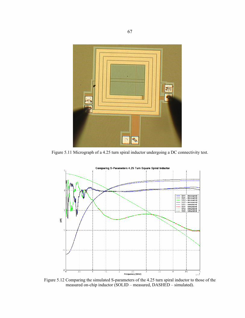
67
Figure 5.11 Micrograph of a 4.25 turn spiral inductor undergoing a DC connectivity test.
Figure 5.12 Comparing the simulated S-parameters of the 4.25 turn spiral inductor to those of the measured on-chip inductor (SOLID – measured, DASHED – simulated).

68
expected, DC connectivity was successfully verified (probing method shown in Figure
5.11).
A point of error in the initial 2-dimensional (2D) method-of-moment modeling of
the 4.25 turn square spiral inductors was the lack of inclusion of the 17,000Å
oxide/nitride passivation layer shown in Figure 3.2. Further simulation of the spiral
inductor with the passivation layer modeled entirely as silicon nitride (Si3N4) indicated
that the inclusion of the layer will in fact lower the self-resonant frequency of the
inductor, but fails to explain the measured behavior below 1GHz. A comparison between
the input matching and through S-parameters is shown in Figure 5.13.
Figure 5.13 Comparing effects of including Si3N4 passivation layer on the simulated S-parameters of the 4.25 turn spiral inductor using IE3D (SOLID – with, DASHED – without).
The entire layer was chosen to be modeled as Si3N4 due to fact that the dielectric
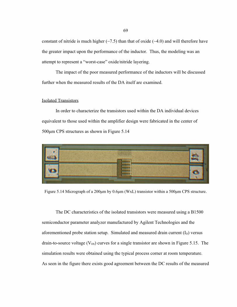
69
constant of nitride is much higher (~7.5) than that of oxide (~4.0) and will therefore have
the greater impact upon the performance of the inductor. Thus, the modeling was an
attempt to represent a “worst-case” oxide/nitride layering.
The impact of the poor measured performance of the inductors will be discussed
further when the measured results of the DA itself are examined.
Isolated Transistors
In order to characterize the transistors used within the DA individual devices
equivalent to those used within the amplifier design were fabricated in the center of
500μm CPS structures as shown in Figure 5.14
Figure 5.14 Micrograph of a 200μm by 0.6μm (WxL) transistor within a 500μm CPS structure.
The DC characteristics of the isolated transistors were measured using a B1500
semiconductor parameter analyzer manufactured by Agilent Technologies and the
aforementioned probe station setup. Simulated and measured drain current (ID) versus
drain-to-source voltage (VDS) curves for a single transistor are shown in Figure 5.15. The
simulation results were obtained using the typical process corner at room temperature.
As seen in the figure there exists good agreement between the DC results of the measured
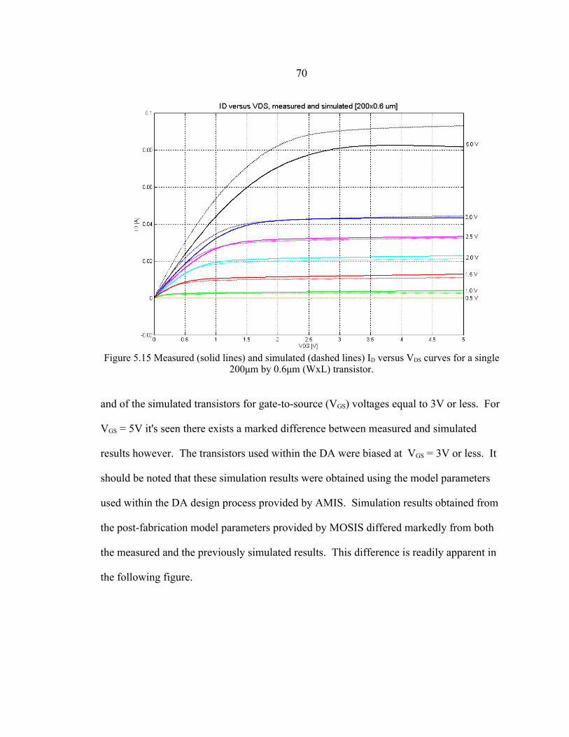
70
Figure 5.15 Measured (solid lines) and simulated (dashed lines) ID versus VDS curves for a single 200μm by 0.6μm (WxL) transistor.
and of the simulated transistors for gate-to-source (VGS) voltages equal to 3V or less. For
VGS = 5V it's seen there exists a marked difference between measured and simulated
results however. The transistors used within the DA were biased at VGS = 3V or less. It
should be noted that these simulation results were obtained using the model parameters
used within the DA design process provided by AMIS. Simulation results obtained from
the post-fabrication model parameters provided by MOSIS differed markedly from both
the measured and the previously simulated results. This difference is readily apparent in
the following figure.

71
Figure 5.16 Simulated ID versus VDS curves for a single 200μm by 0.6μm (WxL) transistor using BSIM3v3 model parameters provided by AMIS (dashed) and MOSIS (solid).
In addition to the DC measurements, results were obtained for the RF
performance of the individual transistors as well. Measured results can be seen compared
to those obtained through simulation of a representative device in Figures 5.17 and 5.18.

72
Figure 5.17 Measured (solid lines) and simulated (dashed lines) gain and input matching of a 200μm by 0.6μm (WxL) transistor.
Figure 5.18 Measured (solid lines) and simulated (dashed lines) reverse isolation and output matching of a 200μm by 0.6μm (WxL) transistor.

73
Both sets of results shown include the effects of the input and output 50Ω CPS
(250μm in length) as a SOLT calibration was performed. Recall that an SOLT
calibration places the reference plane at the tips of the probes without de-embedding any
of the TLs. While a TRL calibration would have allowed de-embedding of the input and
output CPS, it was found that the gain of the transistors disappear at frequencies below
the minimum for which the fabricated TRL standards would allow accurate calibration.
Looking at Figure 5.17, there appears to be good agreement between the measured
and simulated results to approximately 1GHz. After 1GHz however, simulation predicts
that the transistor should provide more than 5dB of gain past 5GHz, whereas
measurements indicate that the transistor loses all gain by 5GHz in a 50Ω system. The
measured input matching appears better than simulated beyond 1GHz. The fact that the
transistor loses gain prematurely is a contributing, although not believed to be the
primary, reason the DA exhibits the poor frequency discussed below.
Figure 5.18 shows the remaining two sets of S-parameters of the transistor,
namely the reverse isolation and the output matching. This figure indicates that there is
relatively good agreement between the measured and simulated results, particularly so for
the reverse isolation.
In order to further discern the differences observed between the measured and
simulated RF performance of the individual transistors it was next decided that inclusion
of a finite gate resistance should be investigated. The layout of the individual transistors
used within the DA circuit were drawn as multi-fingered devices comprised of ten fingers
of width and length 200μm and 0.6μm, respectively; see Figure 5.19. The gate was
contacted on both sides, giving the effect of the equivalent of twenty devices each with
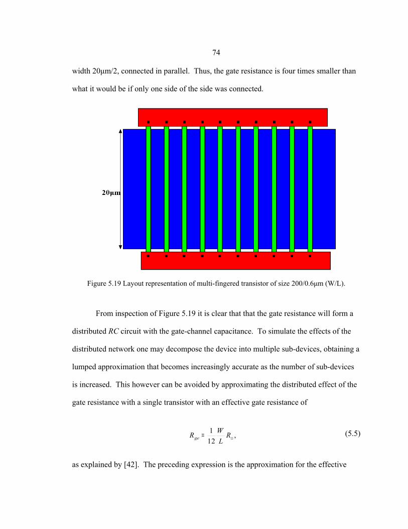
74
width 20μm/2, connected in parallel. Thus, the gate resistance is four times smaller than
what it would be if only one side of the side was connected.
Figure 5.19 Layout representation of multi-fingered transistor of size 200/0.6μm (W/L).
From inspection of Figure 5.19 it is clear that that the gate resistance will form a
distributed RC circuit with the gate-channel capacitance. To simulate the effects of the
distributed network one may decompose the device into multiple sub-devices, obtaining a
lumped approximation that becomes increasingly accurate as the number of sub-devices
is increased. This however can be avoided by approximating the distributed effect of the
gate resistance with a single transistor with an effective gate resistance of
(5.5)
as explained by [42]. The preceding expression is the approximation for the effective
1 ,12ge
WR RL
= W
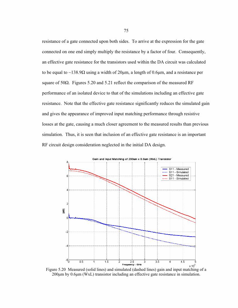
75
resistance of a gate connected upon both sides. To arrive at the expression for the gate
connected on one end simply multiply the resistance by a factor of four. Consequently,
an effective gate resistance for the transistors used within the DA circuit was calculated
to be equal to ~138.9Ω using a width of 20μm, a length of 0.6μm, and a resistance per
square of 50Ω. Figures 5.20 and 5.21 reflect the comparison of the measured RF
performance of an isolated device to that of the simulations including an effective gate
resistance. Note that the effective gate resistance significantly reduces the simulated gain
and gives the appearance of improved input matching performance through resistive
losses at the gate, causing a much closer agreement to the measured results than previous
simulation. Thus, it is seen that inclusion of an effective gate resistance is an important
RF circuit design consideration neglected in the initial DA design.
Figure 5.20 Measured (solid lines) and simulated (dashed lines) gain and input matching of a 200μm by 0.6μm (WxL) transistor including an effective gate resistance in simulation.

76
Figure 5.21 Measured (solid lines) and simulated (dashed lines) reverse isolation and output matching of a 200μm by 0.6μm (WxL) transistor including an effective gate resistance in
simulation.
Distributed Amplifier
The final device to be characterized was the DA itself. The entire DA consists of
six individual 200μm by 0.6μm (WxL) transistors connected by gate and drain CPS delay
lines, two each square planar spiral inductors on the gate and drain line, and one 1200μm
by 0.6μm (WxL) grounded-gate n-type MOSFET (GGNMOS) transistor providing
electrostatic-discharge (ESD) protection at each DC bias input (2 total). The total
fabricated DA can be seen in the micrograph shown in Figure 5.22.

77
Figure 5.22 Micrograph of the fabricated distributed amplifier.
Though designed for an operating point of VDS = VGS = 2.5V, it was discovered
experimentally that the DA exhibited the best performance with VDS = 3.5V and VGS =
1.9V. The measured 2-port S-parameters of the DA after an SOLT calibration from
10MHz to 5GHz are shown in Figure 5.23. The DA was found to exhibit acceptable
input and output matching with an input return loss (S11) of better than 10dB to 10GHz
and an output return loss (S22) better than 8dB to 10GHz (better than 10dB for most of the
range). Return isolation (S12) is good, being better than 25dB to 10GHz. Finally, the
10dB of gain (S21) at low frequency quickly vanishes beyond approximately 650MHz,
whereas design simulation predicted that amplification would persist beyond 9GHz (see
Figures 5.24 and 5.25) at these bias levels. So, while the low frequency gain exceeds
prediction, the low cutoff frequency of the DA is obviously quite disappointing.
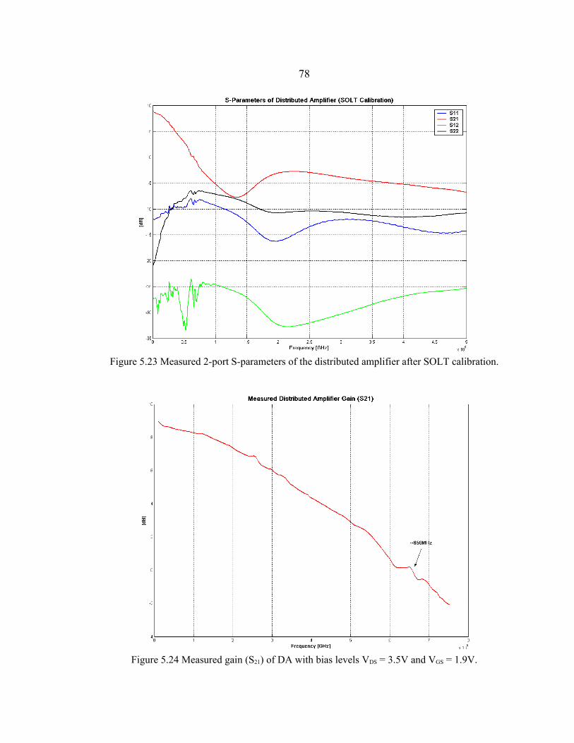
78
Figure 5.23 Measured 2-port S-parameters of the distributed amplifier after SOLT calibration.
Figure 5.24 Measured gain (S21) of DA with bias levels VDS = 3.5V and VGS = 1.9V.

79
Figure 5.25 Simulated gain (S21) of DA with bias levels VDS = 3.5V and VGS = 1.9V.
Based upon the fact that the DC and RF performance results of the isolated
transistors and the phase velocity difference of the gate and drain line are reasonably
close to that which was predicted (although the gain of the individual transistors exhibit a
much lower cutoff frequency than initially simulated), whereas the measured behavior of
the square spiral inductors differs greatly from that predicted, it is believed that the poor
high-frequency gain performance of the DA may be traced in large measure to ill-
performing RF-chokes.
As a first attempt to determine if in fact the on-chip inductors are the root cause of
the poor performance seen the DA's measured results, the measured S-parameters of a
single 4.25 turn spiral inductor were substituted for the 2D modeled inductors in the
simulated DA circuit. Figure 5.26 displays the results of this simulation in terms of gain
and input matching from 10MHz to 1GHz. It is readily apparent that the inductors reduce
the predicted gain from beyond 7GHz (shown in Figure 5.25) to approximately 850MHz
2 4 6 8 10 12 140 16
0
-5
5
freq, GHz
dB
(S(2
,1))
Readout
m1
m1freq=dB(S(2,1))=0.045
9.290GHz

80
when the measured S-parameters are utilized in the simulation. These results clearly
suggest that the fabricated on-chip inductors are greatly limiting the DA's frequency
response.
Figure 5.26 Measured (solid lines) and simulated (dashed lines) gain (S21) and input matching (S11) of the DA. Simulation results include measured data from the on-chip inductors.

81
CHAPTER 6
CONCLUSIONS AND RECOMMENDATIONS FOR FURTHER RESEARCH
S ummary
A distributed, or traveling-wave, amplifier has been designed, fabricated, and
tested using a commercial CMOS process technology. The technology used was the
AMIS C5 process available through the MOSIS service. This process has a 0.6μm
minimum feature size and contains three aluminum metal layers. Funding for the die
fabrication was provided through a MOSIS Educational Program grant.
Both SOLT and TRL calibration techniques were utilized in the characterization
of the RF performance of both passive and active devices. Measured calibration
standards, both on and off chip validated the accuracy of the derived error correction
models. The isolated transistors performed as predicted at DC and exhibited expected RF
performance to about 1GHz, at which point the measured gain dropped more rapidly than
expected in initial simulations. Further simulations of isolated transistors with an
effective gate resistance show stronger agreement to measured results. The phase
velocities of individual sections of the coplanar strip-lines implementing the gate and
drain transmission lines were shown to agree closely with simulation. The on-chip spiral
inductors were found be resonant far below the predicted 4.5GHz however. The
distributed amplifier itself was shown to display gain above predicted, approximately
10dB, at low frequency and then quickly degrade to zero at about 650MHz, much below
the roughly 9GHz bandwidth predicted through simulation. After importing the
measured scattering parameters of the inductors into simulation, it was shown how the
poor performance of the fabricated spiral inductors significantly degrades the frequency

82
response of the distributed amplifier to the point where the gain is predicted to drop to
unity at approximately 850MHz.
Recommendations for Further Work
Planar Spiral Inductors
Fully understanding the performance of the on-chip spiral inductors would seem
to be the most important task at this point in the research. This work may proceed by
attempting to more accurately model the spiral inductors using a full-wave
electromagnetic simulation software package such as that present in Ansoft's High
Frequency Structure Simulator (HFSS). Initial 2D method-of-moments simulation
appear to indicate that failing to include the passivation layer within the models during
the spiral inductor design does not have a significant impact upon the inductor
performance. The spurious S-parameter results obtained from on-chip inductor
measurements below 1GHz appear to suggest that there exists still some unexplained
effects that could be discovered through accurate 3D modeling.
Additionally, the effects of the passivation may be experimentally deduced
through selective etching of the silicon nitride layer using the on-site tools available in
the Montana Microfabrication Facility (MMF). The etching process must be selective to
both aluminum metal and silicon dioxide making the most appropriate choice of process
a dry etch one. The reactive ion etching (RIE) system present within the MMF may be
used for just a procedure. Measured results after etching may then be compared to the
initial design simulations and those with a silicon dioxide layer representative of that
which the etching procedure did not remove. The thickness of the latter is easily

83
determined through using the facility's profilometer.
Planar Microwave Circuit Design Course
The forty fabricated die will also be incorporated into future offerings of the
Planar Microwave Circuit Design course at Montana State University. The chips will
allow future students to obtain hands-on laboratory experiences in on-wafer calibration
and transistor characterization. A portion of the author's remaining duties will be to
construct a simple, straightforward user-manual for such calibrations and measurements
using the hardware (probe station, semiconductor device analyzer, VNA, etc.) and
software (MultiCAL, StatistiCAL, etc.) present within Montana State's Microwave and
mm-Wave Electronics Laboratory.

84
REFERENCES CITED
[1] IBM, “BiCMOS – Key Technology Specifications,” http://www-03.ibm.com/chips/asics/foundry/technologies/bicmosspecs.html
[2] W. Hafez and M. Feng, “Experimental demonstration of pseudomorphic heterojunction bipolar transistors with cutoff frequencies above 600 GHz,” Applied Physics Letters, vol. 86, no. 15, 152101, April 2005.
[3] W. S. Percival, “Thermionic Valve Circuits,” British Patent Specification no. 460,562, filed 24 July 1936, granted January 1937.
[4] E. L. Ginzton, W. R. Hewlett, J. H. Jasberg, and J. D. Noe, “Distributed Amplification,” Proc. IRE, pp. 956-69, August 1948.
[5] E. W. Strid and K. R. Gleason, “A DC-12 GHz Monolithic GaAsFET Distributed Amplifier,” IEEE Trans. Microwave Theory and Techniques, vol. MTT-30, no. 7, pp. 969-975, July 1982.
[6] Y. Ayasli, R. L. Mozzi, J. L. Vorhaus, L. D. Reynolds, and R. A. Pucel, “A Monolithic GaAs 1-13-GHz Traveling-Wave Amplifier,” IEEE Trans. Microwave Theory and Techniques, vol. MTT-30, no. 7, pp. 976-981, July 1982.
[7] K. B. Niclas, W. T. Wilser, T. R. Kritzer, and R. R. Pereira, “On Theory and Performance of Solid-State Microwave Distributed Amplifiers,” IEEE Trans. Microwave Theory and Techniques, vol. MTT-31, no. 6, pp. 447-456, June 1983.
[8] R. Majidi-Ahy, C. K. Nishimoto, M. Riaziat, M. Glenn, S. Silverman, S.-L. Weng, Y.-C. Pao, G. A. Zdasiuk, S. G. Bandy, and Z. C. H. Tan, “5-100 GHz InP Coplanar Waveguide MMIC Distributed Amplifier,” IEEE Trans. Microwave Theory and Techniques, vol. MTT-38, no. 12, December 1990.
[9] S. Kimura, Y. Imai, Y. Umeda, and T. Enoki, “Loss-compensated Distributed Baseband Amplifier for Optical Transmission Systems,” IEEE Trans. Microwave Theory and Techniques, vol. MTT-44, no. 10, pp. 1688-1693, October 1996.
[10] D. Linten, S. Thijs, W. Jeamsaksiri, J. Ramos, A. Mercha, M. I. Natarajan, P. Wambacq, A. J. Scholten, and S. Decoutere, “An Integrated 5 GHz Low-Noise Amplifier with 5.5 kV HBM ESD protection in 90 nm RF CMOS,” 2005 Symp. on VLSI Circuits Digest of Technical Papers, pp. 86-89, July 16-18 2005.
[11] T. H. Lee, Planar Microwave Engineering: A Practical Guide to Theory, Measurement, and Circuits, Cambridge University Press, 2004.

85
[12] Y. Ayasli, R. L. Mozzi, J. L. Vorhaus, L. D. Reynolds, and R. A. Pucel, “A Monolithic GaAs 1-13-GHz Traveling-Wave Amplifier,” IEEE Trans. Microwave Theory and Techniques, vol. MTT-30, pp. 976-981, July 1982.
[13] D. M. Pozar, Microwave Engineering. 2nd ed., New York: John Wiley & Sons, Inc., 1998.
[14] A. S. Sedra and K. C. Smith, Microelectronic Circuits, 4th ed., New York: Oxford University Press, Inc., 1998.
[15] Agilent Technologies Inc., “Advanced Design System (ADS) 2004A”. Palo Alto, CA, Available: http://eesof.tm.agilent.com/products/ads_main.html
[16] P. H. Woerlee, M. J. Knitel, R. van Langevelde, D. B. M. Klaassen, L. F. Tiemeijer, A. J. Scholten, and A. T. A. Zegers-van Duijnhoven, “RF-CMOS Performance Trends,” IEEE Trans. On Electron Devices, vol. 48, no. 8, pp. 1776-1782, August 2001.
[17] D. Thelen, Personal Communication, AMI Semiconductor, Inc., Bozeman, MT, June, 2006.
[18] J. P. Becker, “S-Parameter Design of Amplifiers,” EE433 – Planar Microwave Circuit Design, Fall 2006 Lectures.
[19] C. H. Doan, S. Emami, A. M. Niknejad, and R. W. Brodersen, “Design of CMOS for 60GHz Applications,” Solid-State Circuits Conference, vol. 1, pp. 440-538, February 2004.
[20] R. A. Pucel, “Design Considerations for Monolithic Microwave Circuits,” IEEE Trans. on Microwave Theory and Techniques, vol. MTT-29, no. 6, pp. 513-534, June 1981.
[21] S. Akhtarzad, T. R. Rowbotham, and P. B. Johns, “The Design of Coupled Microstrip Lines,” IEEE Trans. on Microwave Theory and Techniques, vol. MTT-23, no. 6, pp. 486-492, June 1975.
[22] R. Garg and I. J. Bahl, “Characteristics of Coupled Microstriplines,” IEEE Trans. on Microwave Theory and Techniques, vol. MTT-27, no. 7, pp. 700-705, July 1979.
[23] M. Kirschning and R. H. Jansen, “Accurate Wide-Range Design Equations for the Frequency-Dependent Characteristic of Parallel Coupled Microstrip Lines,” IEEE Trans. on Microwave Theory and Techniques, vol. MTT-32, no. 1, pp. 83-90, January 1984.
[24] T. Q. Deng, M. S. Leong, P. S. Kooi, and T. S. Yeo, “Synthesis formulas for coplanar lines in hybrid and monolithic MICs,” Electronics Letters, vol. 32, no. 24, pp. 2253-2254, November 1996.

86
[25] C. Yildiz, “New and Very Simple Synthesis Formulas for Coplanar Strip Line,” Microwave and Optical Technology Letters, vol. 44, no. 2, pp. 199-202, January 2005.
[26] Zeland Software Inc., “IE3D Version 8.2”, Fremont, CA, Available: http://www.zeland.com
[27] B. Kleveland, C. H. Diaz, D. Vook, L. Madden, T. H. Lee, and S. S. Wong, “Monolithic CMOS Distributed Amplifier and Oscillator,” in IEEE Dig. Tech. Papers, 1999, pp. 70-71.
[28] P. J. Sullivan, B. A. Xavier, and W. H. Ku, “An Integrated CMOS Distributed Amplifier Utilizing Packaging Inductance,” IEEE Trans. on Microwave Theory and Techniques, vol. 45, no. 10, October 1997, pp. 1969-1976.
[29] B. M. Ballweber, R. Gupta, and D. J. Allstot, “A Fully Integrated 0.5-5.5-GHz CMOS Distributed Amplifer,” IEEE Trans. on Solid-State Circuits, vol. 35, no. 2, pp. 231-238, February 2000.
[30] L. N. Alves and R. L. Aguiar, “Frequency Behavior of Classical Current Mirrors,” ICECS 2002 - 9th IEEE Conference on Electronics, Circuits and Systems, Dubrovnik, Croatia, Sep. 2002.
[31] S. S. Mohan, M. Hershenson, S. P. Boyd, and T. H. Lee, “Simple Accurate Expressions for Planar Spiral Inductors”, IEEE Journal of Solid-State Circuits, vol. 43, no. 10, pp. 1419-1424, October 1999.
[32] A. Zolfaghari, A. Chan, and B. Razavi, “Stacked Inductors and Transformers in CMOS Technology,” IEEE Journal of Solid-State Circuits, vol. 36, no. 4, pp.620-628, April 2001.
[33] T. Dickson, M.-A. LaCroix, S. Boret, D. Gloria, R. Beerkens, and S. P. Voinigescu, “Si-based Inductors and Transformers for 30-100 GHz Applications,” Microwave Symposium Digest, 2004 IEEE MTT-S International, vol. 1, pp. 205-208, June, 2004.
[34] Ansoft Corporation, “High Frequency Structure Simulator (HFSS) Ver. 9.2.1”, Tech. Rep., Pittsburgh, PA, 2005. Available: http://www.ansoft.com/products/hf/hfss/
[35] T. H. Lee, The Design of CMOS Radio-Frequency Integrated Circuits, 2nd ed., Cambridge University Press, 2004.
[36] Cadence Design Systems, “Virtuoso Layout Editor,” San Jose, CA, Available: http://www.cadence.com/
[37] Agilent Network Analyzer Basics, Agilent Technologies, Inc., August 31, 2004.
[38] S. A. Wartenberg, RF Measurements of Die and Packages, Artech House, Inc.,

87
2002.
[39] G. F. Engen and C. A. Hoer, “'Thru-Reflect-Line': An Improved Technique for Calibrating the Dual Six-Port Automatic Network Analyzer,” vol. MTT-27, no. 12, pp. 987-993, December 1979.
[40] D. F. Williams, J. C. M. Wang, and U. Arz, “An Optimal Vector-Network Analyzer Calibration Algorithm,” IEEE Trans. on Microwave Theory and Techniques, vol. MTT-51, no. 12, pp. 2391-2401, December 2003.
[41] P. T. Boggs, R. H. Byrd, J. E. Rogers, and R. B. Schnabel, “User's Reference Guide for ODRPACK Version 2.01 Software for Wieghted Orthogonal Distance Regression,” NIST, Boulder, CO, Internal Rep. NISTIR 91-4834, June 1992.
[42] Y. Tsividis, Operation and Modeling of The MOS Transistor, 2nd Ed., Oxford, New York, Oxford University Press, 1999.

88
APPENDICES

89
APPENDIX A
NON-QUASISTATIC EFFECTS

90
Non-quasistatic Effects & CMOS SPICE Models
The majority of MOSFET models implemented in SPICE are based upon
quasistatic (QS) approximations. QS operation assumes that the terminal voltages vary
slowly enough for the channel charge of the MOS transistor to achieve equilibrium
instantaneously [1]. Thus, these charges can be determined using equivalent DC voltages
applied to the terminals. At high-frequencies however, these approximations begin to
breakdown, leading to unpredictable transistor behavior. Attempts to quantify criteria for
the onset of non-quasistatic (NQS) effects based upon transient behavioral simulations
have been proposed by [2] and [3]. These simulation results suggest that the total
inversion charge, given by
(A.1)
when stimulated by a sinusoidal input voltage, deviates from that predicted by the QS
model in both amplitude and phase at sufficiently high frequency. Results presented by
[2] demonstrate that the amplitude remains nearly constant until a certain frequency limit,
while the phase shift varies linearly with phase. Using these results, the non-quasistatic
onset frequency limit fNQS can be defined separately in terms of acceptable inversion layer
amplitude and phase deviation from that of the QS model. The former was found to be
minimal until nearly the unity-gain frequency fT of the devices simulated in both [2] and
[3]. Phase deviation was indicated to range from ~3º at 20% of fT to ~12º at fT.
Typical analog circuits may be designed with a respectable phase margin in order
^'
,0
( ) ( ) sin( )L
inv inv inv DC invQ t Q t dx Q Q t= = + ⋅ ω + φ∫

91
to ensure stable operation, mitigating the requirement of using NQS device modeling.
This phase deviation can create much more significant performance degradation in a DA
design however. Recall that phase velocity equalization is a principle requirement in the
DA. Phase differences of greater than 5º were experimentally shown by the author to
result in significant signal reflections. Using the device parameters indicated in this
thesis, these results indicate that the QS BSIM3v3 model used should only be taken to
accurately simulate the response of the DA up to approximately 5GHz.
[1] Y. Tsividis, Operation and Modeling of the MOS Transistor, 2nd Ed., Oxford University Press, U.S.A., 2003.
[2] E. Gondro, O. Kowarik, G. Knoblinger, and P. Klein, “When do we need Non-Quasistatic CMOS RF-Models?,” Proc. IEEE Custom Integrated Circuits Conf., San Diego, CA, May 2001, pp. 377-380.
[3] A. F.-L. Ng, P. K. Ko, and M. Chan, “Determining the Onset Frequency of Nonquasistatic Effects of the MOSFET in AC Simulation,” IEEE Electron Device Letters, vol. 23, no. 1, January 2002, pp. 37-39.

92
APPENDIX B
AMIS C5 BSIM3V3 SPICE MODEL PARAMETERS(CONFIDENTIAL)

93
APPENDIX C
MOSIS T5AR RUN WAFER ELECTRICAL TEST DATA AND SPICE MODEL PARAMETERS

94
MOSIS WAFER ACCEPTANCE TESTS RUN: T5AR VENDOR: AMIS TECHNOLOGY: SCN05 FEATURE SIZE: 0.5 microns Run type: SKD
INTRODUCTION: This report contains the lot average results obtained by MOSIS from measurements of MOSIS test structures on each wafer of this fabrication lot. SPICE parameters obtained from similar measurements on a selected wafer are also attached.
COMMENTS: American Microsystems, Inc. C5
TRANSISTOR PARAMETERS W/L N-CHANNEL P-CHANNEL UNITS MINIMUM 3.0/0.6 Vth 0.74 -0.94 volts SHORT 20.0/0.6 Idss 459 -242 uA/um Vth 0.64 -0.91 volts Vpt 10.0 -10.0 volts WIDE 20.0/0.6 Ids0 < 2.5 < 2.5 pA/um LARGE 50/50 Vth 0.65 -0.96 volts Vjbkd 11.0 -11.7 volts Ijlk <50.0 <50.0 pA Gamma 0.49 0.57 V^0.5 K' (Uo*Cox/2) 54.6 -18.8 uA/V^2 Low-field Mobility 445.90 153.53 cm^2/V*s COMMENTS: Poly bias varies with design technology. To account for mask bias use the appropriate value for the parameter XL in your SPICE model card. Design Technology XL (um) XW (um) ----------------- ------- ------ SCMOS_SUBM (lambda=0.30) 0.10 0.00 SCMOS (lambda=0.35) 0.00 0.20
FOX TRANSISTORS GATE N+ACTIVE P+ACTIVE UNITS Vth Poly >15.0 <-15.0 volts

95
PROCESS PARAMETERS N+ P+ POLY PLY2_HR POLY2 M1 M2 UNITS Sheet Resistance 82.0 102.6 23.3 1101 41.9 0.09 0.09 ohms/sq Contact Resistance 60.9 146.9 17.1 27.7 0.83 ohms Gate Oxide Thickness 141 angstrom PROCESS PARAMETERS M3 N\PLY N_W UNITS Sheet Resistance 0.05 847 841 ohms/sq Contact Resistance 0.79 ohms COMMENTS: N\POLY is N-well under polysilicon.
CAPACITANCE PARAMETERS N+ P+ POLY POLY2 M1 M2 M3 N_W UNITS Area (substrate) 432 728 85 32 16 10 40 aF/um^2 Area (N+active) 2447 36 16 11 aF/um^2 Area (P+active) 2340 aF/um^2 Area (poly) 911 56 16 9 aF/um^2 Area (poly2) 49 aF/um^2 Area (metal1) 31 13 aF/um^2 Area (metal2) 33 aF/um^2 Fringe (substrate) 351 289 74 58 38 aF/um Fringe (poly) 57 38 28 aF/um Fringe (metal1) 54 33 aF/um Fringe (metal2) 51 aF/um Overlap (N+active) 214 aF/um Overlap (P+active) 231 aF/um
CIRCUIT PARAMETERS UNITS Inverters K Vinv 1.0 1.97 volts Vinv 1.5 2.23 volts Vol (100 uA) 2.0 0.12 volts Voh (100 uA) 2.0 4.86 volts Vinv 2.0 2.41 volts Gain 2.0 -18.60

96
Ring Oscillator Freq. DIV256 (31-stg,5.0V) 100.83 MHz D256_WIDE (31-stg,5.0V) 152.64 MHz Ring Oscillator Power DIV256 (31-stg,5.0V) 0.50 uW/MHz/gate D256_WIDE (31-stg,5.0V) 1.01 uW/MHz/gate COMMENTS: SUBMICRON
T5AR SPICE BSIM3 VERSION 3.1 PARAMETERS
SPICE 3f5 Level 8, Star-HSPICE Level 49, UTMOST Level 8
* DATE: Dec 19/05* LOT: T5AR WAF: 9102* Temperature_parameters=Default.MODEL CMOSN NMOS ( LEVEL = 49+VERSION = 3.1 TNOM = 27 TOX = 1.41E-8+XJ = 1.5E-7 NCH = 1.7E17 VTH0 = 0.586875+K1 = 0.8563109 K2 = -0.0870606 K3 = 21.2216405+K3B = -8.2868264 W0 = 1E-8 NLX = 1E-9+DVT0W = 0 DVT1W = 0 DVT2W = 0+DVT0 = 2.6056345 DVT1 = 0.4382785 DVT2 = -0.1735756+U0 = 456.0277023 UA = 2.415709E-12 UB = 1.416873E-18+UC = 4.598182E-12 VSAT = 1.92885E5 A0 = 0.5967346+AGS = 0.1129858 B0 = 2.667003E-6 B1 = 5E-6+KETA = -9.709638E-4 A1 = 1.170959E-5 A2 = 0.3031839+RDSW = 1.264411E3 PRWG = 0.0767006 PRWB = 0.0181561+WR = 1 WINT = 1.950485E-7 LINT = 7.18413E-8+XL = 1E-7 XW = 0 DWG = -4.687723E-9+DWB = 5.083626E-8 VOFF = 0 NFACTOR = 0.3386768+CIT = 0 CDSC = 2.4E-4 CDSCD = 0+CDSCB = 0 ETA0 = 2.048127E-3 ETAB = -1.791953E-4+DSUB = 0.0684107 PCLM = 2.546561 PDIBLC1 = 1+PDIBLC2 = 2.474758E-3 PDIBLCB = -0.0168243 DROUT = 0.9735435+PSCBE1 = 6.377329E8 PSCBE2 = 2.095166E-4 PVAG = 9.989289E-3+DELTA = 0.01 RSH = 82 MOBMOD = 1+PRT = 0 UTE = -1.5 KT1 = -0.11+KT1L = 0 KT2 = 0.022 UA1 = 4.31E-9+UB1 = -7.61E-18 UC1 = -5.6E-11 AT = 3.3E4+WL = 0 WLN = 1 WW = 0+WWN = 1 WWL = 0 LL = 0+LLN = 1 LW = 0 LWN = 1+LWL = 0 CAPMOD = 2 XPART = 0.5+CGDO = 2.14E-10 CGSO = 2.14E-10 CGBO = 1E-9+CJ = 4.309065E-4 PB = 0.97442 MJ = 0.4323804+CJSW = 3.255079E-10 PBSW = 0.8 MJSW = 0.2023408+CJSWG = 1.64E-10 PBSWG = 0.8 MJSWG = 0.2023408+CF = 0 PVTH0 = 0.1279055 PRDSW = -183.5626587+PK2 = -0.0273762 WKETA = -0.018498 LKETA = 3.588525E-

97
3 )*.MODEL CMOSP PMOS ( LEVEL = 49+VERSION = 3.1 TNOM = 27 TOX = 1.41E-8+XJ = 1.5E-7 NCH = 1.7E17 VTH0 = -0.9239325+K1 = 0.5474696 K2 = 7.884255E-3 K3 = 5.7895228+K3B = -1.0529775 W0 = 2.392135E-7 NLX = 9.013808E-8+DVT0W = 0 DVT1W = 0 DVT2W = 0+DVT0 = 2.4409049 DVT1 = 0.479078 DVT2 = -0.0812137+U0 = 202.7748917 UA = 2.492512E-9 UB = 1E-21+UC = -7.05979E-11 VSAT = 1.518724E5 A0 = 0.7338304+AGS = 0.095815 B0 = 1.07472E-6 B1 = 4.99995E-6+KETA = -8.151786E-4 A1 = 7.117004E-4 A2 = 0.3261133+RDSW = 3E3 PRWG = -0.0422194 PRWB = -0.0192246+WR = 1 WINT = 2.300175E-7 LINT = 9.660331E-8+XL = 1E-7 XW = 0 DWG = -8.177807E-9+DWB = 1.723601E-8 VOFF = -0.0604473 NFACTOR = 0.735806+CIT = 0 CDSC = 2.4E-4 CDSCD = 0+CDSCB = 0 ETA0 = 0.4947532 ETAB = -0.0743284+DSUB = 1 PCLM = 2.3713952 PDIBLC1 = 0.0317803+PDIBLC2 = 3.060557E-3 PDIBLCB = -0.0531146 DROUT = 0.1834052+PSCBE1 = 5.297294E9 PSCBE2 = 5E-10 PVAG = 0.0132388+DELTA = 0.01 RSH = 102.6 MOBMOD = 1+PRT = 0 UTE = -1.5 KT1 = -0.11+KT1L = 0 KT2 = 0.022 UA1 = 4.31E-9+UB1 = -7.61E-18 UC1 = -5.6E-11 AT = 3.3E4+WL = 0 WLN = 1 WW = 0+WWN = 1 WWL = 0 LL = 0+LLN = 1 LW = 0 LWN = 1+LWL = 0 CAPMOD = 2 XPART = 0.5+CGDO = 2.31E-10 CGSO = 2.31E-10 CGBO = 1E-9+CJ = 7.256029E-4 PB = 0.9506215 MJ = 0.4987322+CJSW = 2.85532E-10 PBSW = 0.99 MJSW = 0.2661054+CJSWG = 6.4E-11 PBSWG = 0.99 MJSWG = 0.2661054+CF = 0 PVTH0 = 5.98016E-3 PRDSW = 14.8598424+PK2 = 3.73981E-3 WKETA = 5.300715E-3 LKETA = -5.899284E-3 )*

98
APPENDIX D
IE3D EXTRACTED RLGC PARAMETERS FOR 500mm, 50Ω CPS

99
The frequency dependent equivalent circuit parameters:
Warning: The error function for 11 GHz and higher frequency is quite high (0.253373>0.25).The single RLC-equivalent circuit may not be a suitable one for it. Please checkits accuracy before use the data.
Freq (GHz) Error Factor Q-Factor Series R (Ohms) Series L (nH) Shunt R (Ohms) Shunt C (pF)
0.25 0.0095961 0.54493 0.84954 0.29484 90003 0.12661 0.5 0.018877 1.0209 0.88947 0.28928 23031 0.12482 0.75 0.027704 1.4212 0.93968 0.28381 10685 0.12175 1 0.03601 1.7565 0.99382 0.27849 6371.6 0.11788 1.25 0.043789 2.0437 1.0476 0.27357 4373.3 0.11352 1.5 0.051075 2.2973 1.0985 0.26917 3285.9 0.10895 1.75 0.05792 2.5277 1.146 0.26532 2628.7 0.10437 2 0.064386 2.741 1.1899 0.26198 2201.2 0.099957 2.25 0.070534 2.9409 1.2306 0.25906 1907.3 0.095792 2.5 0.07642 3.1297 1.2686 0.25649 1696.5 0.091935 2.75 0.082094 3.3088 1.3041 0.25421 1540 0.088409 3 0.087599 3.4795 1.3376 0.25215 1420.6 0.085214 3.25 0.092972 3.6427 1.369 0.25028 1327.2 0.082336 3.5 0.098243 3.7995 1.3986 0.24857 1252.8 0.079753 3.75 0.10344 3.9507 1.4263 0.24699 1192.4 0.07744 4 0.10857 4.0971 1.4523 0.24552 1142.7 0.075371 4.25 0.11367 4.2394 1.4765 0.24414 1101.1 0.073518 4.5 0.11873 4.3781 1.4991 0.24284 1066.1 0.07186 4.75 0.12378 4.5137 1.5199 0.24162 1036.1 0.070372 5 0.12881 4.6468 1.5392 0.24047 1010.3 0.069036 5.25 0.13384 4.7776 1.5569 0.23938 987.85 0.067835 5.5 0.13888 4.9064 1.573 0.23833 968.17 0.066752 5.75 0.14391 5.0335 1.5876 0.23734 950.8 0.065774 6 0.14896 5.1591 1.6008 0.23639 935.36 0.06489 6.25 0.15401 5.2833 1.6127 0.23547 921.55 0.064089 6.5 0.15908 5.4062 1.6232 0.2346 909.12 0.063362 6.75 0.16416 5.5281 1.6324 0.23375 897.88 0.0627 7 0.16926 5.6489 1.6403 0.23293 887.66 0.062098 7.25 0.17437 5.7687 1.647 0.23214 878.33 0.061549 7.5 0.1795 5.8877 1.6526 0.23137 869.76 0.061047 7.75 0.18465 6.0058 1.6571 0.23063 861.86 0.060589 8 0.18982 6.1231 1.6604 0.2299 854.54 0.060169 8.25 0.195 6.2396 1.6628 0.22919 847.74 0.059785 8.5 0.20021 6.3554 1.6641 0.22849 841.39 0.059432 8.75 0.20543 6.4705 1.6644 0.22781 835.44 0.059109 9 0.21067 6.5849 1.6638 0.22714 829.85 0.058812 9.25 0.21594 6.6985 1.6622 0.22649 824.57 0.05854 9.5 0.22122 6.8115 1.6597 0.22584 819.57 0.058289 9.75 0.22653 6.9238 1.6564 0.2252 814.81 0.05806 10 0.23185 7.0355 1.6522 0.22457 810.27 0.057849 10.25 0.2372 7.1464 1.6472 0.22395 805.93 0.057656 10.5 0.24257 7.2567 1.6414 0.22333 801.76 0.057479 10.75 0.24796 7.3664 1.6348 0.22272 797.74 0.057316 11 0.25337 7.4753 1.6275 0.22212 793.85 0.057168 11.25 0.25881 7.5835 1.6194 0.22151 790.08 0.057033 11.5 0.26427 7.6911 1.6105 0.22092 786.42 0.056909 11.75 0.26975 7.798 1.601 0.22032 782.84 0.056797 12 0.27525 7.9041 1.5908 0.21973 779.34 0.056696 12.25 0.28078 8.0095 1.5799 0.21913 775.91 0.056604 12.5 0.28633 8.1142 1.5683 0.21854 772.53 0.056522 12.75 0.2919 8.2181 1.5561 0.21796 769.19 0.056449 13 0.2975 8.3212 1.5432 0.21737 765.9 0.056383 13.25 0.30312 8.4235 1.5297 0.21678 762.63 0.056326 13.5 0.30877 8.525 1.5156 0.21619 759.38 0.056276 13.75 0.31445 8.6257 1.5009 0.2156 756.14 0.056233 14 0.32015 8.7255 1.4857 0.21501 752.91 0.056196 14.25 0.32587 8.8244 1.4698 0.21442 749.69 0.056166 14.5 0.33163 8.9224 1.4534 0.21383 746.45 0.056142 14.75 0.33741 9.0194 1.4364 0.21324 743.21 0.056124 15 0.34321 9.1155 1.4189 0.21264 739.95 0.056111

100
APPENDIX E
ANALYTICAL PLANAR SPIRAL INDUCTOR DESIGN
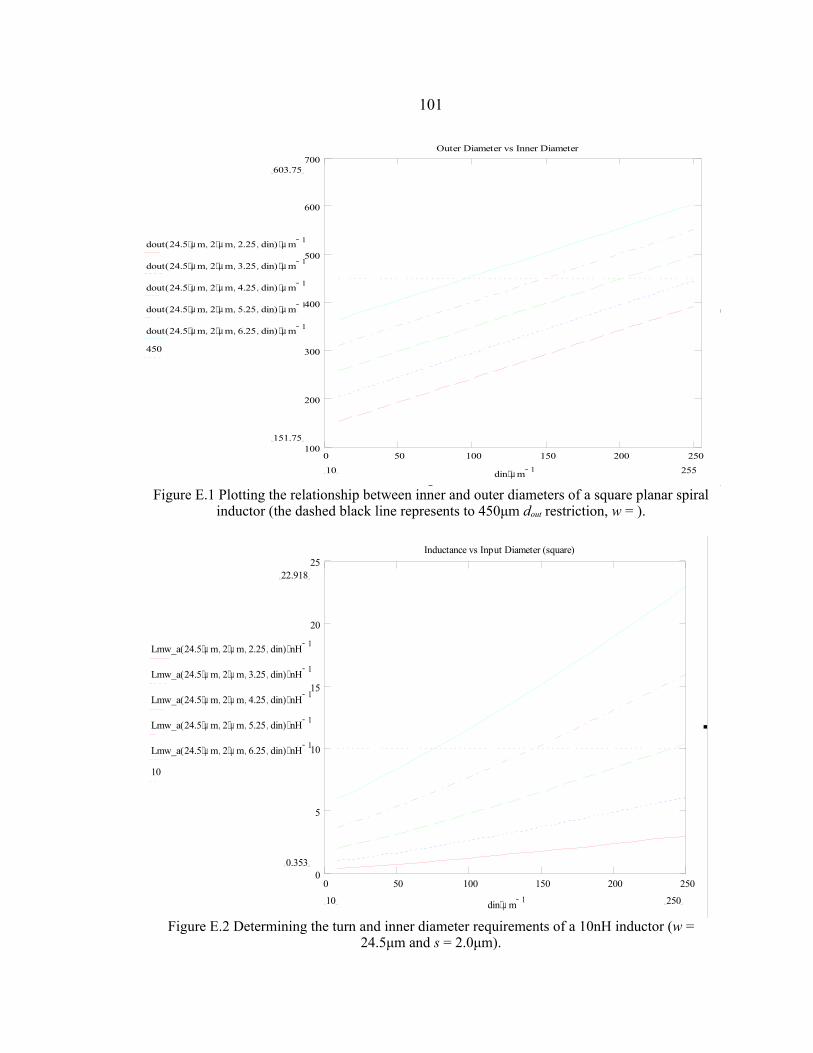
101
Figure E.1 Plotting the relationship between inner and outer diameters of a square planar spiral inductor (the dashed black line represents to 450μm dout restriction, w = ).
Figure E.2 Determining the turn and inner diameter requirements of a 10nH inductor (w = 24.5μm and s = 2.0μm).
0 50 100 150 200 250100
200
300
400
500
600
700Outer Diameter vs Inner Diameter
603.75
151.75
dout 24.5 µ m⋅ 2 µ m⋅, 2.25, din,( ) µ m 1−⋅
dout 24.5 µ m⋅ 2 µ m⋅, 3.25, din,( ) µ m 1−⋅
dout 24.5 µ m⋅ 2 µ m⋅, 4.25, din,( ) µ m 1−⋅
dout 24.5 µ m⋅ 2 µ m⋅, 5.25, din,( ) µ m 1−⋅
dout 24.5 µ m⋅ 2 µ m⋅, 6.25, din,( ) µ m 1−⋅
450
25510 din µ m 1−⋅
0 50 100 150 200 250100
200
300
400
500
600
700Outer Diameter vs Inner Diameter
dout 24.5 µ m⋅ 2 µ m⋅, 2.25, din,( ) µ m 1−⋅
dout 24.5 µ m⋅ 2 µ m⋅, 3.25, din,( ) µ m 1−⋅
dout 24.5 µ m⋅ 2 µ m⋅, 4.25, din,( ) µ m 1−⋅
dout 24.5 µ m⋅ 2 µ m⋅, 5.25, din,( ) µ m 1−⋅
dout 24.5 µ m⋅ 2 µ m⋅, 6.25, din,( ) µ m 1−⋅
450
din µ m 1−⋅
0 50 100 150 200 2500
5
10
15
20
25Inductance vs Input Diameter (square)
22.918
0.353
Lmw_a 24.5 µ m⋅ 2 µ m⋅, 2.25, din,( ) nH 1−⋅
Lmw_a 24.5 µ m⋅ 2 µ m⋅, 3.25, din,( ) nH 1−⋅
Lmw_a 24.5 µ m⋅ 2 µ m⋅, 4.25, din,( ) nH 1−⋅
Lmw_a 24.5 µ m⋅ 2 µ m⋅, 5.25, din,( ) nH 1−⋅
Lmw_a 24.5 µ m⋅ 2 µ m⋅, 6.25, din,( ) nH 1−⋅
10
25010 din µ m 1−⋅
0 50 100 150 200 2500
2
4
6
8
10
12
14
16Inductance vs Input Diameter (circle)
Lgmd_d 5 µ m⋅ 5 µ m⋅, 2.25, din,( ) nH 1−⋅
Lgmd_d 5 µ m⋅ 5 µ m⋅, 3.25, din,( ) nH 1−⋅
Lgmd_d 5 µ m⋅ 5 µ m⋅, 4.25, din,( ) nH 1−⋅
Lgmd_d 5 µ m⋅ 5 µ m⋅, 5.25, din,( ) nH 1−⋅
din µ m 1−⋅

102
Figure E.2 Plotting the effects of winding width on square planar spiral inductance (n = 4.25, s = 2.0μm).
Figure E.3 Plotting the effects on winding spacing on inductance of square spiral inductor.
0 10 20 30 40 500
5
10
15
20
25
30Inductance vs Spacing (square)
26.667
2.484
Lmw_a 24.5 µ m⋅ spacing, 2.25, 213.3 µ m⋅,( ) nH 1−⋅
Lmw_a 24.5 µ m⋅ spacing, 3.25, 213.3 µ m⋅,( ) nH 1−⋅
Lmw_a 24.5 µ m⋅ spacing, 4.25, 213.3 µ m⋅,( ) nH 1−⋅
Lmw_a 24.5 µ m⋅ spacing, 5.25, 213.3 µ m⋅,( ) nH 1−⋅
Lmw_a 24.5 µ m⋅ spacing, 6.25, 213.3 µ m⋅,( ) nH 1−⋅
501 spacing µ m 1−⋅
0 50 100 150 200 2500
2
4
6
8
10
12Comparing Widths vs Input Dia. (square)
10.829
1.038
Lmw_a 10 µ m⋅ 2 µ m⋅, 4.25, din,( ) nH 1−⋅
Lmw_a 20 µ m⋅ 2 µ m⋅, 4.25, din,( ) nH 1−⋅
Lmw_a 25 µ m⋅ 2 µ m⋅, 4.25, din,( ) nH 1−⋅
Lmw_a 30 µ m⋅ 2 µ m⋅, 4.25, din,( ) nH 1−⋅
25510 din µ m 1−⋅
0 50 100 150 200 2500
2
4
6
8
10
12Comparing Circle & Square vs Input Diam.
Lgmd_a 24.5 µ m⋅ 2 µ m⋅, 4.25, din,( ) nH 1−⋅
Lgmd_d 24.5 µ m⋅ 2 µ m⋅, 4.25, din,( ) nH 1−⋅
din µ m 1−⋅

103
Figure E.4 Comparing inductance of circle and square spiral inductor geometries with equal dimensions.
0 50 100 150 200 2500
2
4
6
8
10
12Comparing Circle & Square vs Input Diam.
10.498
1.767
Lgmd_a 24.5 µ m⋅ 2 µ m⋅, 4.25, din,( ) nH 1−⋅
Lgmd_d 24.5 µ m⋅ 2 µ m⋅, 4.25, din,( ) nH 1−⋅
25510 din µ m 1−⋅