does fpga-based prototyping really have to be this...
TRANSCRIPT
Does FPGA-based prototyping really have to be this difficult?
Embedded Conference Finland
Andrew MarshallMay 2017

2 © 2017 Cadence Design Systems, Inc. All rights reserved.
What is FPGA-Based Prototyping?
• Primary platform for pre-silicon software development and validation
• Maps a digital ASIC, ASSP, SoC design or part thereof into one or more FPGAs
• Allows SW to simulate in real world environments
• Provides pre-silicon execution speeds in MHz • Enables connectivity to real peripherals
• Runs real world traffic flows including interrupts and unpredictable events
• Runs error conditions and handling errata with other system components

3 © 2017 Cadence Design Systems, Inc. All rights reserved.
FPGA-Based Prototyping as part of your verification solution
• Ever-increasing verification requirements driven by growing hardware and software complexity
• Fast time to results is essential to ensure projects can meet schedules
• Right tools for the right job: Combination of formal, simulation, emulation and FPGA prototyping
Project timeline
Formal
Simulation
FPGA Prototyping
Emulation
Tapeout
Mai
n co
re e
ngin
e us
age
Silicon
…
…
…
…

4 © 2017 Cadence Design Systems, Inc. All rights reserved.
FPGA-based prototyping is hard to do
Clocking Memories
Debug
Interfaces
Software
5 © 2017 Cadence Design Systems, Inc. All rights reserved.
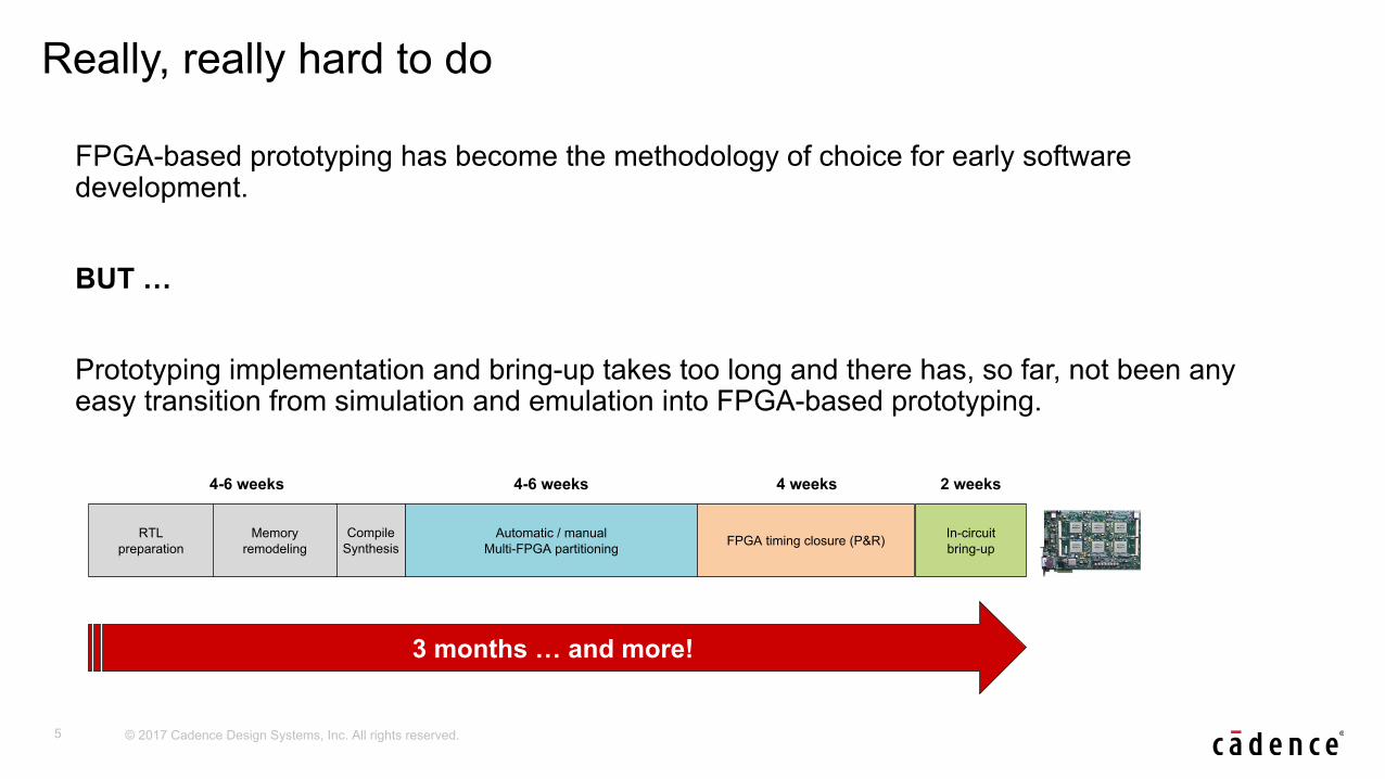
Really, really hard to do
FPGA-based prototyping has become the methodology of choice for early software development.
BUT …
Prototyping implementation and bring-up takes too long and there has, so far, not been any easy transition from simulation and emulation into FPGA-based prototyping.
RTLpreparation
CompileSynthesis
Automatic / manualMulti-FPGA partitioning FPGA timing closure (P&R) In-circuit
bring-upMemory
remodeling
4-6 weeks 4-6 weeks 4 weeks 2 weeks
3 months … and more!
6 © 2017 Cadence Design Systems, Inc. All rights reserved.
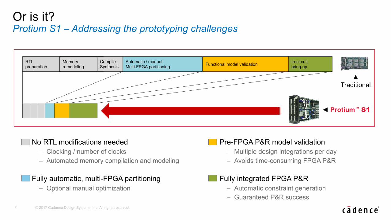
Or is it?Protium S1 – Addressing the prototyping challenges
• No RTL modifications needed– Clocking / number of clocks– Automated memory compilation and modeling
• Fully automatic, multi-FPGA partitioning– Optional manual optimization
• Pre-FPGA P&R model validation– Multiple design integrations per day– Avoids time-consuming FPGA P&R
• Fully integrated FPGA P&R– Automatic constraint generation– Guaranteed P&R success
RTLpreparation
CompileSynthesis
Automatic / manualMulti-FPGA partitioning Functional model validation In-circuit
bring-upMemoryremodeling
▲Traditional
◄ Protium™ S1

7 © 2017 Cadence Design Systems, Inc. All rights reserved.
Advanced clocking – any type and number
• Protium™ benefits:– No hold-time violations in user clock domains– Removes any FPGA-specific clock limitations– Supports unlimited # of design clocks– Improves FPGA timing closure– Accelerates FPGA P&R times
• Traditional imitations:– Gated clock, multiplexed clocks– # of clocks– Difficult to achieve FPGA timing closure– Long iteration times / long FPGA P&R times– Unpredictable results & prototype behavior
Clock distribution on the board Clock generation in the FPGA
8 © 2017 Cadence Design Systems, Inc. All rights reserved.
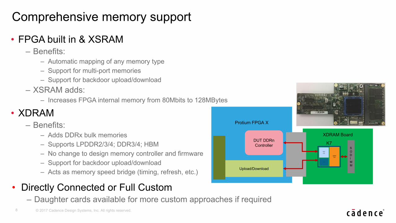
Comprehensive memory support
• FPGA built in & XSRAM– Benefits:
– Automatic mapping of any memory type– Support for multi-port memories– Support for backdoor upload/download
– XSRAM adds:– Increases FPGA internal memory from 80Mbits to 128MBytes
• XDRAM– Benefits:
– Adds DDRx bulk memories– Supports LPDDR2/3/4; DDR3/4; HBM– No change to design memory controller and firmware– Support for backdoor upload/download– Acts as memory speed bridge (timing, refresh, etc.)
Protium FPGA X
XDRAM BoardDUT DDRnController
SODIMM
Upload/Download
DDR3 Ctrl
DDRnI/f
Logic
UD Module
K7
• Directly Connected or Full Custom– Daughter cards available for more custom approaches if required

9 © 2017 Cadence Design Systems, Inc. All rights reserved.
Hardware and software debug
Application Specific Components
SoC interconnect fabric
ARM V8 CPUSubsystem
3DGFX
DSP A/V
High speed, wired interface peripherals
DDR3
PHY
Other peripherals
SATA
MIPI
HDMI
WLAN
LTE Low-speed peripheral subsystem
Low speed peripherals
PMU
MIPIJTAG
INTC
I2C
SPITime
r
GPIO
Display
UART
Boot processo
rARM M0
ModemCortex-A53
L2 cache
USB3.0
3.0PHY
2.0PHY
PCIeGen 2,3
PHY
Ether
net
PHY
Cortex-A53
Cortex-A57
L2 cache
CortexA57
Cache coherent fabric
SoC, Sub-System or IP
Low-SpeedPeripherals
General-Purpose
Peripherals
High Speed,Wired Interface
Peripherals
Customer’sApplication-Specific Components
ComputeSub System
Operating Systems (OS)Drivers
ApplicationsMiddleware
Firmware / HAL
Software
UART – to peripherals
Hardware Debug: RTL
Probes
• Waveforms across partitions• Design-centric view vs. FPGA-centric
• Force/release• Predefined signals (at compile time) to “0”
or “1” during runtime• Monitor signal
• Real-time monitoring of predefined (at compile time) signals
Software Debug: C Code
JTAG
• Backdoor memory access• Quickly change boot code, software, etc.
• Clock control • Start/stop the clock on demand
• Fully scriptable runtime environment• Remote access
• Network resource anytime from anywhere• High-performance link to software model

10 © 2017 Cadence Design Systems, Inc. All rights reserved.
Scalable performance
5MHz
10MHz
100MHz
Automatic mode Further Optimization
Phase 1
Phase 2
3MHz
Performance(single board, multi-FPGA)
Prototypingdesign
Phase 3
Design-based user manual refinement
Higher effortperformanceoptimization
Automaticfor quick
functionality
…

11 © 2017 Cadence Design Systems, Inc. All rights reserved.
0 5 10 15 20 25 30 35
Mobile
Networking
Consumer
CPU
Consumer
Networking
Networking
TraditionalProtiumS1
Fast Time-to-Prototype (TTP)
Bring-up time (weeks)
◄ 81%
◄ 85%
◄ 88%
◄ 91%
◄ 89%
◄ 91%
◄ 79%
Note: Sample customer bring-up gains over traditional FPGA-based Prototyping solutions
“Protium™ has incredibly simplified our prototyping flow. It allowed us to significantly improve prototyping bring-up time.”
Riad Ben MouhoubPhD/Tech Leader, Microsemi Corporation

12 © 2017 Cadence Design Systems, Inc. All rights reserved.
Microsemi @ CDNLive … challenges & requirements

13 © 2017 Cadence Design Systems, Inc. All rights reserved.
… and this is what our customers are saying!Amlogic @ DAC 2016

14 © 2017 Cadence Design Systems, Inc. All rights reserved.
… and Xilinx likes it too
“The Cadence Protium S1 platform ensures scalability to hundreds of software developers at the earliest possible point during the development flow, and allows developers to focus on design validation and software development rather than prototype bring-up. The common flow with the Cadence Palladium Z1 emulation platform enables a smooth transition from emulation to prototyping, which greatly improves productivity.”
-Peter Ryser, Senior Director for System Software, Integration, and Validation, Xilinx
15 © 2017 Cadence Design Systems, Inc. All rights reserved.
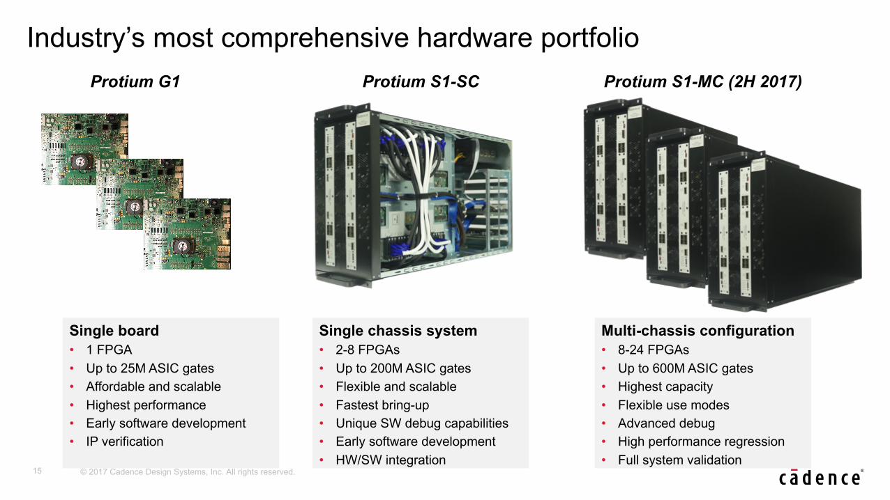
Industry’s most comprehensive hardware portfolio
Single board• 1 FPGA• Up to 25M ASIC gates• Affordable and scalable• Highest performance• Early software development• IP verification
Single chassis system• 2-8 FPGAs• Up to 200M ASIC gates• Flexible and scalable• Fastest bring-up• Unique SW debug capabilities• Early software development• HW/SW integration
Multi-chassis configuration• 8-24 FPGAs• Up to 600M ASIC gates• Highest capacity• Flexible use modes• Advanced debug • High performance regression• Full system validation
Protium G1 Protium S1-SC Protium S1-MC (2H 2017)
16 © 2017 Cadence Design Systems, Inc. All rights reserved.
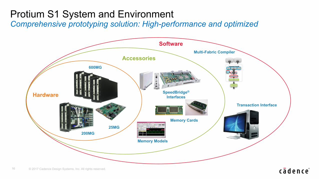
Accessories
Software
SpeedBridge®
Interfaces
Memory Cards
Hardware
25MG200MG
600MG
Memory Models
FPGA bit files
Integrated Compile EngineHDL-ICE
for fastcompile
Partitioning
FPGA P&R
Memory compiler
Debug inserter
Board router
Board file
ASIC RTL(Verilog / VHDL /
SV)
Debug probes and trigger conditions
Multi-Fabric Compiler
Transaction Interface
Protium S1 System and EnvironmentComprehensive prototyping solution: High-performance and optimized

17 © 2017 Cadence Design Systems, Inc. All rights reserved.
Protium S1 – the Most Efficient Way to Prototype Your ASIC
• Fast time-to-prototyping (months down to weeks)– No RTL changes– Automatic partitioning/memory compilation– Fully integrated FPGA place-and-route
• Scalable performance (3-100MHz)– From fully automatic to fully manual– Advanced black-box methodology
• Advanced software debug– Memory upload/download– Force and release– SCE-MI transaction interface

© 2017 Cadence Design Systems, Inc. All rights reserved worldwide. Cadence, the Cadence logo and the other Cadence marks found at www.cadence.com/go/trademarks are trademarks or registered trademarks of Cadence Design Systems, Inc. All other trademarks are the property of their respective holders. PCI Express and PCIe are registered trademarks of PCI-SIG.