dielectric surface imaging using scanning electron microsope
TRANSCRIPT
Dielectric surface imaging using Scanning Electron Microscope
Vinaykrishnan k11-521

The Scanning Electron Microscope
Principle: The basic principle is that a beam of electrons is
generated by a suitable source, typically a tungsten filament or a field emission gun.
The electron beam is accelerated through a high voltage (e.g.: 20 kV) and pass through a system of apertures and electromagnetic lenses to produce a thin beam of electrons.
Then the beam scans the surface of the specimen Electrons are emitted from the specimen by the action of the scanning beam and collected by a suitably-positioned detector.

Construction
• Scanning Electron Microscope’s basic components are as following…
Electron gun (Filament)Condenser lensesObjective ApertureScan coilsChamber (specimen test)DetectorsComputer hardware and software

The Scanning Electron Microscope

Electron Guns
Electron guns are typically one of TWO types.1) Thermionic guns2) Field emission guns
1) Thermionic guns: Which are the most common type, apply
thermal energy to a filament to coax electrons away from the gun and toward the specimen under examination.
Usually made of tungsten, which has a high melting point

Electron Guns
2) Field emission guns: Create a strong electrical field to pull
electrons away from the atoms they‘re associated with.
Electron guns are located either at the very top or at the very bottom of an SEM and fire a beam of electrons at the object under examination.
These electrons don't naturally go where they need to, however, which gets us to the next component of SEMs.

Electron Guns

Condenser Lenses
The Condenser lenses are made of magnets capable of bending the path of electrons.
By doing so, the Condenser lenses focus and control the electron beam, ensuring that the electrons end up precisely where they need to go.

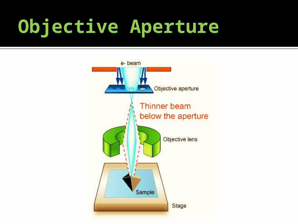
Objective Aperture
The objective aperture arm fits above the objective lens in the SEM. It is a metal rod that holds a thin plate of metal containing four holes. Over this fits a much thinner rectangle of metal with holes (apertures) of different sizes. By moving the arm in and out different sized holes can be put into the beam path.
An aperture holder: this arm holds a thin metal strip with different sized holes that line up with the larger holes. The metal strip is called an Aperture strip.
The aperture stops electrons that are off-axis or off-energy from progressing down the column. It can also narrow the beam below the aperture, depending on the size of the hole selected.
Objective Aperture

Scan Coils
The scanning coils consist of two solenoids oriented in such a way as to create two magnetic fields perpendicular to each other.
Varying the current in one solenoid causes the electrons to move left to right.
Varying the current in the other solenoid forces these electrons to move at right angles to this direction (left to right) and downwards.

Chamber (Specimen Test)
The specimen(dielectric material) is placed on a teflon holder.
This isolates the dielectric material from typically mounted aluminium stub on which a sample is usually placed for imaging in SEM.
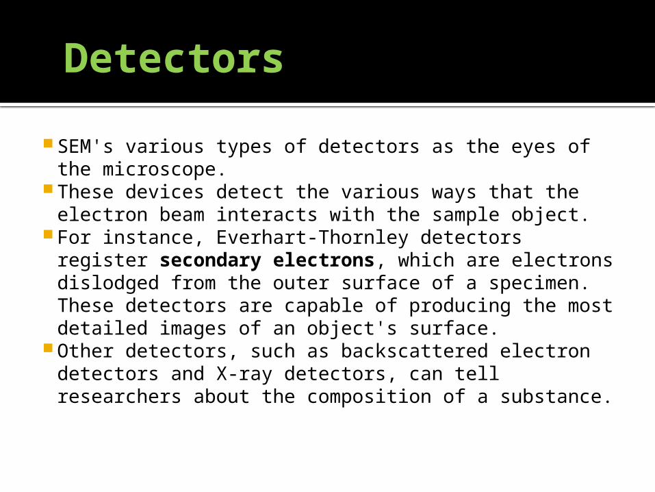
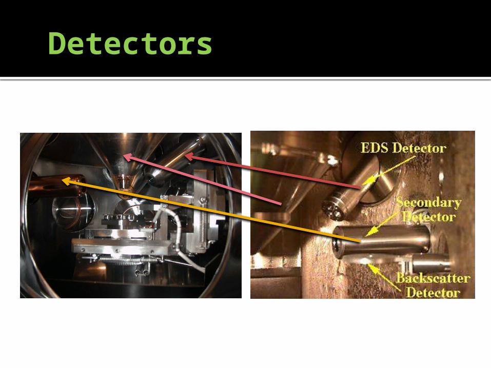
Detectors
SEM's various types of detectors as the eyes of the microscope.
These devices detect the various ways that the electron beam interacts with the sample object.
For instance, Everhart-Thornley detectors register secondary electrons, which are electrons dislodged from the outer surface of a specimen. These detectors are capable of producing the most detailed images of an object's surface.
Other detectors, such as backscattered electron detectors and X-ray detectors, can tell researchers about the composition of a substance.
Detectors

Sample preparation

Sample preparation
Cleaning of dielectric surface Stabilization of dielectric material Rinsing of material Dehydration of surface Drying of surface
Problems
Charging effect takes place on the surface of dielectric material due to electron irradiation.
As a result, electrostatic charge formation occurs due to charge trapping by the dielectric material.
Moreover various surface defects characterized by surface roughness, microstructural lattice damages also lead to electrostatic charge formation.

Solutions

Solutions
Coating the dielectric surface with a thin layer of approx. 20-30 nm conductive metal(gold, gold-palladium, platinum) which is grounded.

Solutions
Applying a defocused flux of soft landing positive ions.
Applying high energy electrons on dielectric surface followed by bombardment of low energy electrons.
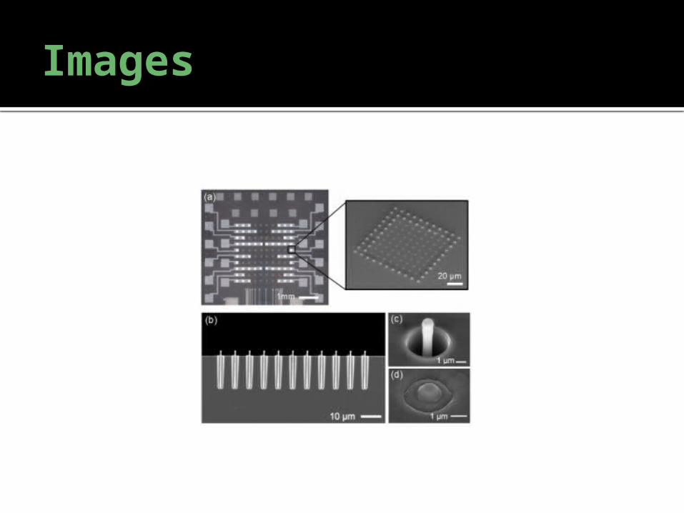
Images
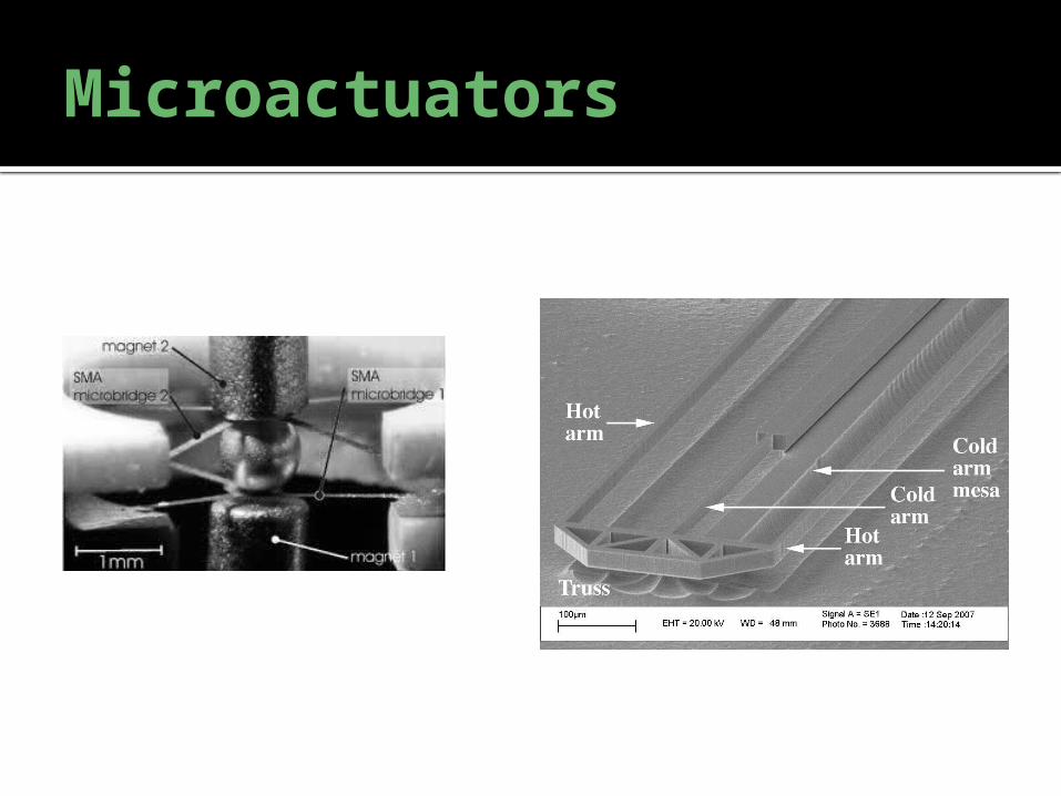
Microactuators

Thank you