designing an integrated all-optical analog to digital
TRANSCRIPT
International Journal of Optics and Photonics (IJOP) Vol. 14, No. 1, Winter-Spring, 2020
3
Designing an Integrated All-Optical Analog to Digital
Converter
Sajjad Moshfea, Mohammad Kazem Moravvej-Farshi
b,*, Kambiz Abedi
c
aDepartment of Electrical Engineering, Science and research branch, Islamic Azad University,
Tehran, Iran bNano Plasmo-Photonic Research Group, Faculty of Electrical and Computer Engineering,
Tarbiat Modares University, Tehran, Iran
cDepartment of Electrical and Computer Engineering, Shahid Beheshti University, Tehran,
Iran
Corresponding author Email: [email protected]
Regular paper: Received: Jun. 16, 2019, Revised: Oct. 2, 2019, Accepted: Nov. 2, 2019,
Available Online: June. 30, 2020, DOI: 10.29252/ijop.14.1.3
ABSTRACT— We present the procedure for
designing a high speed and low power all-
optical analog to digital converter (AO-ADC),
by integrating InGaAsP semiconductor optical
amplifier (SOA) with InP based photonic
crystal (PhC) drop filters. The self-phase
modulation in the SOA can shift the frequency
of the Gaussian input pulse. The two output
PhC based drop filters are designed to
appropriately code the frequency-shifted
analog signals by the SOA, converting them to
four desired digital output levels. Our
numerical results show that in an appropriately
designed AO-ADC, the center wavelength (1572
nm) of an amplitude modulated Gaussian pulse
of 1.8 ps width and 1.56 pJ energy can be
shifted by 6.7 nm, by the SOA, and then be
quantized and coded to four digital levels (00,
01, 10, and 11). The two point-defect PhC drop
filters, compensating the effect of the frequency
shift by SOA, minimize the AO-ADC integral
and differential nonlinearity errors.
KEYWORDS: Semiconductor Optical Amplifier
(SOA), Self-Phase Modulation (SPM),
Photonic Crystal (PhC), Analog to Digital
Converter (ADC).
I. INTRODUCTION
Continuous nature of the real world signals
makes an analog to digital converter (ADC) an
inseparable part of any digital process. An
electronic ADC faces with a few challenging
issues, such as the jitter of the sampling
window and the ambiguity of the comparator.
To overcome these issues, researchers have
proposed semi-optical ADC [1, 2]. Moreover,
various all-optical ADCs (AO-ADCs) have
also been proposed in this regard [3-20]. An
AO-ADC consists of a mode-locked laser,
generating high speed pulses with ultra-low
jitters, as the sampling part, an optical
quantizer, and an optical coder. The optical
ADC designers have substituted the latter two
optical parts for the electronic parts in a semi-
optical ADC to enhance its conversion speed
[3].
The Kerr effect has been rigorously used in the
design of the AO-ADCs. In the early ’90s, a 3-
bit AO-ADC was developed experimentally,
using the cross-phase modulation of a 200-m
single mode fiber loop employed as a
nonlinear interferometer [4]. A decade later, a
4-bit ADC based on hard limiters was
presented [5]. The hard limiters consist of
alternating layers of materials having different
Kerr nonlinearities. Other techniques such as
self-frequency shifting [6, 7], slicing super-
continuum spectrum [8], and self-phase
modulation (SPM) [9] in a long linear or
nonlinear fiber were also used to design AO-
ADCs. Later, employing the self-frequency
S. Moshfe et al. Designing an Integrated All-Optical Analog to Digital Converter
4
shift and SPM induced spectral compression in
a highly nonlinear fiber, a 4-bit ADC operating
at 100 Gb/s were designed [10]. They
employed the self-frequency shifting to
quantize the analog signal and used the
spectral compression to improve the
resolution. Nevertheless, all these fiber-based
ADCs, reported so far, have exploited long
fibers that require high input power that makes
it unsuitable for integration. Following the
same trend, by using the multistage approach
for SPM-based spectral compression in fiber
and improving the spectral compression ratio
more than twice, a 5-bit AO-ADC was
achieved, a few years later [11]. Then,
replacing the high-nonlinear fiber with a
shorter photonic crystal fiber an AO-ADC with
the 6-bit resolution was achieved [12].
Recently, a group has employed intensity-to-
wavelength conversion by soliton self-
frequency shift and experimentally
demonstrated a 40-Gs/s AO-ADC. [13].
Meanwhile, the integrable optical ADC based
on a semiconductor optical amplifier (SOA)
was first reported in [14]. In this design, the
cross-gain modulation of SOA was used to
quantize a four-level signal at 20 Gs/s and
code it into 2 bits. However, as the number of
the quantization levels (N) is increased for
high-resolution applications, this design faces
two problematic issues: (i) the complexity of
the ADC structure, requiring 2N+1 SOAs; (ii)
the quantization levels becomes hardly
distinct. In an alternative design, another
research group has exploited polarization
switches based on the nonlinear polarization
rotation in SOA to achieve a 3-bit ADC
operating at hundreds of Gs/s [15]. Later on,
using multiple rectangular bandpass filters to
digitize the chirped probe signal passing
through a quantum dot (QD)-SOA, another
research group has revealed a two-bit SOA-
based AO-ADC, operating at 10 Gs/s with an
8-level optical quantization [16].
Furthermore, an alternative method to achieve
an integrable all-optical ADC is to exploit the
Kerr nonlinearities in a photonic crystal (PhC).
In this regard, exploiting two-channel drop
filters coupled with a cavity-based wavelength
selective reflector, a PhC-based 2 bit ADC
with no coder has been proposed [17]. Another
group has reported the design of a two-bit
PhC-based ADC with a coder, employing a
nonlinear demultiplexer to quantize the input
analog signal and a coder to convert the
quantized levels into a 2-bit binary code [18,
19]. With the aid of an appropriate reflector in
conjunction with a hexagonal PhC waveguide,
a 2-bit AO-ADC has been designed without
the need for any coder [20]. The authors have
shown their design could improve operation
speed, without discussing the decrease in its
nonlinearities.
In this paper, we are introducing an integrated
two-bit optical ADC, consisting of an SOA as
a nonlinear optical quantizer integrated with
two-channel drop filters devised on a single
PhC platform to act as an optical coder. Unlike
the fiber-based ADCs, the new design is
integrable to InP-based photonic chips and can
operate with much less optical input power.
Moreover, it is possible to increase its
resolution by altering the configuration of the
optical coder without a need for an extra SOA,
consuming less cross-sectional area and
requiring less complicated electronic circuitry.
This integrated ADC, unlike the PhC-based
ADCs, can operate with no need for exploiting
a nonlinear PhC. Besides, the integration of
SOA and PhC helps to decrease the ADCs
integral nonlinearity (INL) and differential
nonlinearity (DNL) errors.
The rest of this paper is organized as follows.
Section 2 is devoted to a description of the
proposed integrated ADC structure and the
basic design principles. In Section 3, we
present the simulation results and the related
discussions. Finally, we conclude the paper
with conclusive remarks in Section 4.
II. INTEGRATED OPTICAL ADC
A. Proposed Structure
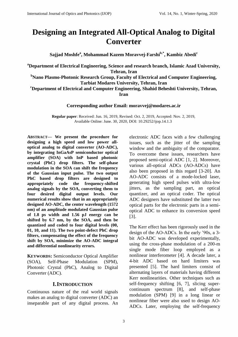
Figure 1 illustrates a 3D schematic
representation of the proposed integrated
International Journal of Optics and Photonics (IJOP) Vol. 14, No. 1, Winter-Spring, 2020
5
optical ADC, composed of an InP-based
traveling wave (TW) SOA, whose active
region is made of In1−xGaxAsyP1−y, integrated
with two drop filters devised on an InP pillar
PhC platform. Details of the SOA and PhC
physical and geometrical parameters are given
in Section 3.
Fig. 1. 3D schematic representation of the proposed
integrated optical ADC.
B. Operating principle
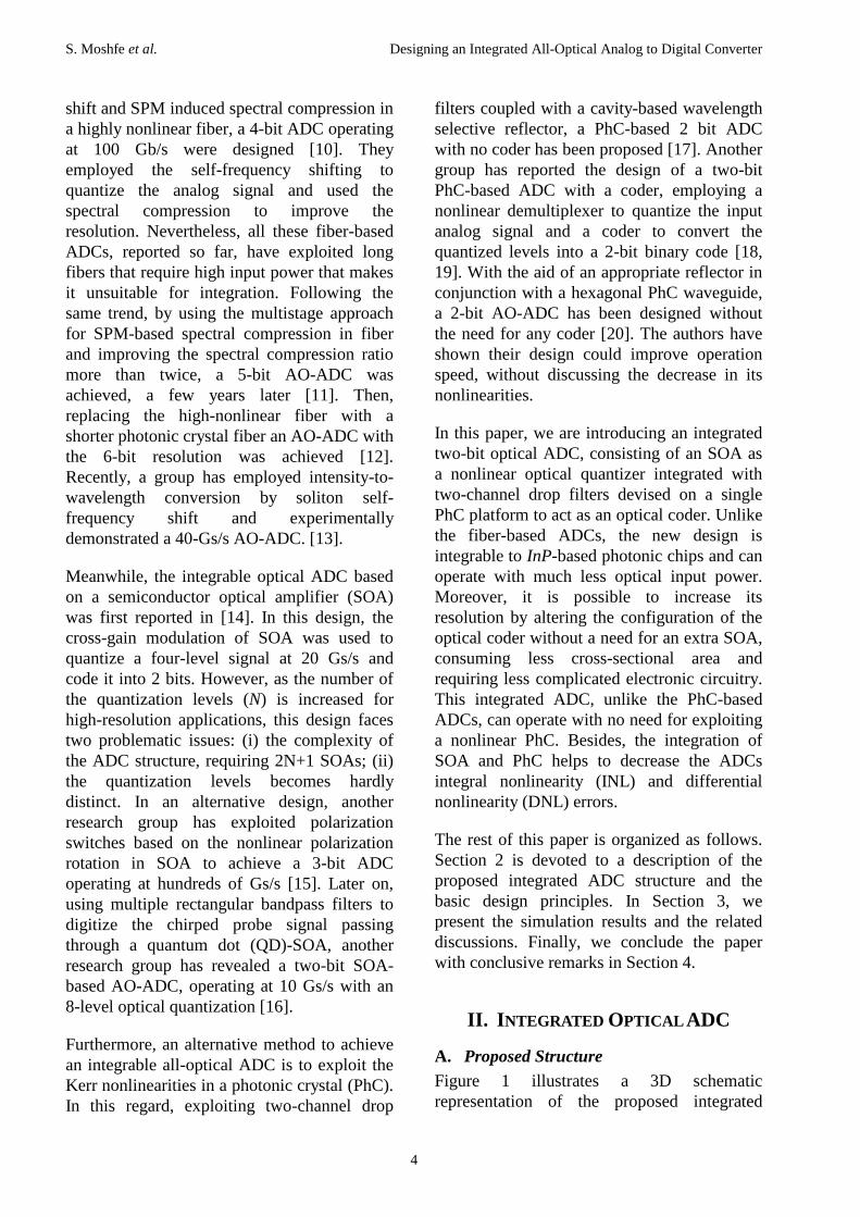
The operating principles of the proposed
integrated optical ADC are based on the SPM
nonlinear effect in the SOA. Consider a given
modulated Gaussian pulse chain as an input
optical signal, as schematically illustrated in
Fig. 2. The signal at the SOA output, due to
the SOA long gain recovery time, exhibits a
frequency chirp that depends on the input
pulse energy. After passing through the PhC-
based drop filters, the chirped signal is
quantized into a four-level coded signal.
Fig. 2. Schematic of the optical ADC operating
principle.
The PhC-based filters are appropriately
designed to produce the Gray-code (i.e., 00,
01, 11, and 10). For this purpose, the filter
bandwidth determines the pulsewidth of the
input pulse. Moreover, to have four distinct
output levels, the design is aimed to obtain the
maximum possible shift for any given
pulsewidth.
C. SPM-Induced frequency chirp
The SPM nonlinearity of an SOA, due to its
long gain recovery time, is sensitive to the
input pulse amplitude. Pulse propagation
models in SOA has already been developed by
others [20-22]. Employing the model
developed by [20], one can describe the
evolution of an optical pulse in an SOA by the
following three coupled equations:
0
sat
;g
c
vg gg gPt
E z
(1a)
int
Pg P
z
(1b)
1
2g
z
(1c)
where z and t are the space and time
coordinates, g, and P and φ represent the gain,
and the pulse amplitude and phase at position z
at any instant 𝜏, 𝜏c, VG, αint, and α are the
spontaneous carrier lifetime, signal group
velocity in the active medium, internal loss,
and the linewidth enhancement factor.
Moreover,
0 0 0 1Ng a N I I (2a)
is the small-signal gain with Γ, aN, N0, and I,
representing the confinement factor, gain
coefficient, transparency carrier density, and
the injection current. Moreover, for an active
layer of length l, width w, and thickness d the
transparency current is I0=qVN0/τc with q and
V=wdl being the electron charge and active
layer volume. Furthermore,
sat 0 NE a (2b)
is the saturation energy, where ħ, ω0, and
σ=wd/Γ are the reduced Planck’s constant,
pulse radian frequency, and the mode cross-
section.
S. Moshfe et al. Designing an Integrated All-Optical Analog to Digital Converter
6
Integrating (1a)-(1c) over the SOA length and
ignoring the internal loss for the case in which
αint≪g, we get:
in0
sat
exp 1c
Pg ld
d E
GGG (3a)
out in expP P G (3b)
out in
1
2 G (3c)
where 0
,
l
g z dz G represents the
integral gain at any instant 𝜏, on the given
temporal Gaussian input pulse of energy Ein
and time constant 𝜏0,
2
inin 2
00
exp .2
EP
(4)
After solving (3a) numerically for G(τ), one
can obtain the output pulse spectrum, by (3b)
and its Fourier transform.
Any change in the phase with time corresponds
to a chirp in the output signal frequency,
outout .
2
d d
d d
G (5)
Using the relation between the wavelength (λ)
and radian frequency (5) leads to the resulting
shift in the output wavelength
2
out .2
d
c d
G (6)
It has already been shown that for an input
temporal pulse of width ∆𝜏1/2=2(2ln2)1/2𝜏0, the
larger the unsaturated single-pass gain of the
amplifying cavity (i.e., G0 = exp (g0l)( the
larger the shift in the wavelength of the
chirped signal (∆λout). Moreover, for an SOA
under a certain biasing condition that leads to
the maximum G0, one may increase the shift in
the chirped signal wavelength, using a
narrower temporal pulse [20]. However, for
the latter case, an increase in ∆λout can be
achieved at the expense of an increase in the
signal frequency or wavelength bandwidth
(∆ω1/2 or ∆λ1/2). Recalling that for a Gaussian
temporal pulse of given ∆𝜏1/2, the wavelength
bandwidth is given by ∆λ1/2=−(λ2/c) ∆ω1/2=
−0.44(λ2/c∆𝜏1/2), according to the time-
bandwidth product limitation for an ultra-short
Gaussian pulse. Hence, for an appropriately
designed PhC drop filter to be able to code the
chirped signals correctly, one needs to choose
a Gaussian pulse of suitable width.
D. PhC Filter
To provide a coded digital output, the SOA
output should be integrated into two
appropriately designed PhC based bandpass
filters, with relatively low-quality factors and
wide passbands, overlapping over the desired
frequency range. Each designed filter is
composed of a point defect cavity coupled to a
line defect waveguide, similar to that of [17],
devised within a pillar PhC platform on the
same InP substrate used for SOA.
III. RESULTS AND DISCUSSION
The 2D finite difference time domain (FDTD)
numerical method is employed to simulate the
dynamic behavior of the integrated optical
ADC of Fig. 1.
A. Frequency Chirp
Consider a commercial SOA (CIP
Technologies, model SOA-XN-OEC-1550)
[25] and employing the constant parameters
given in Table 1, solving (2a) and (2b), one
gets Esat= 0.5 pJ and g0=76.5 cm−1 (G0≈33
dB).
First, using (3)-(6) we calculate the amount of
the redshift (∆λout) versus the normalized pulse
energy (Ein/Esat) for different temporal pulses
of widths 1 ps ≤∆𝜏1/2≤ 10 ps, as illustrated in
Fig 3(a). As can be observed from this figure,
the redshift, for any given pulsewidth, is a
sublinear function of the input pulse energy.
Furthermore, for given input energy, the
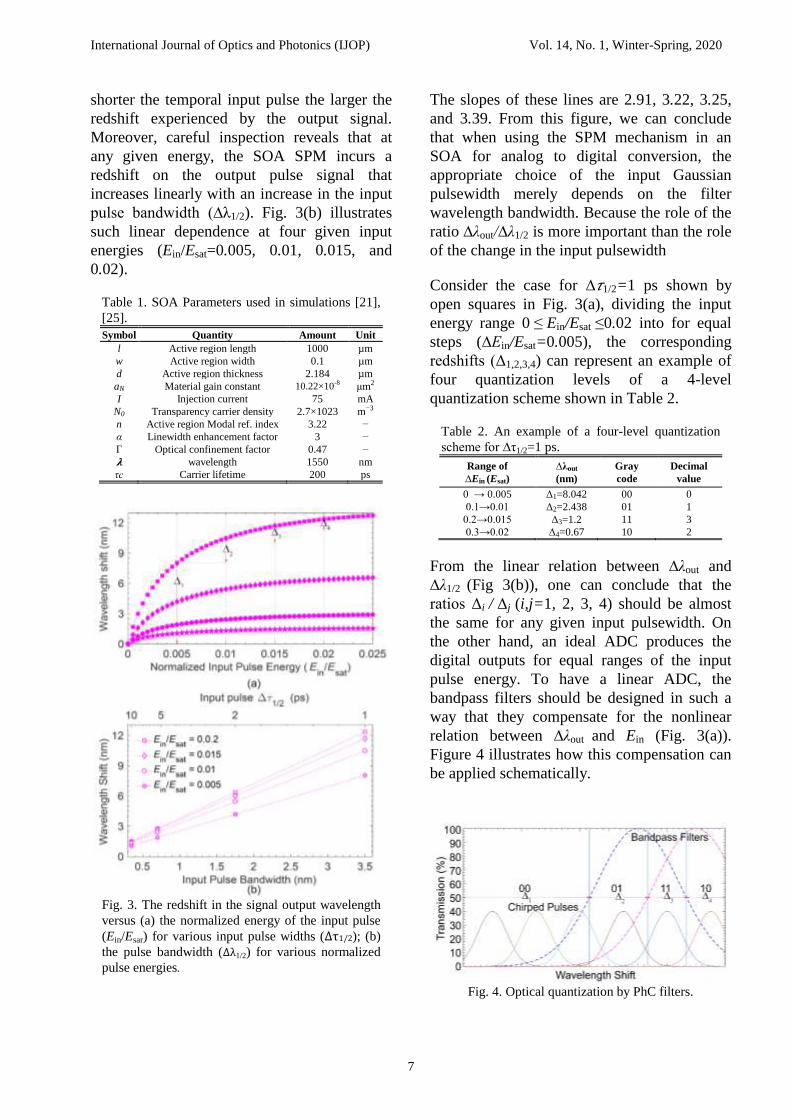
International Journal of Optics and Photonics (IJOP) Vol. 14, No. 1, Winter-Spring, 2020
7
shorter the temporal input pulse the larger the
redshift experienced by the output signal.
Moreover, careful inspection reveals that at
any given energy, the SOA SPM incurs a
redshift on the output pulse signal that
increases linearly with an increase in the input
pulse bandwidth (∆λ1/2). Fig. 3(b) illustrates
such linear dependence at four given input
energies (Ein/Esat=0.005, 0.01, 0.015, and
0.02).
Table 1. SOA Parameters used in simulations [21],
[25].
Symbol Quantity Amount Unit
l Active region length 1000 µm
w Active region width 0.1 µm
d Active region thickness 2.184 µm
aN Material gain constant 10.22×10⁻⁸
μm2
I Injection current 75 mA
N0 Transparency carrier density 2.7×10²³ m−3
n Active region Modal ref. index 3.22 −
α Linewidth enhancement factor 3 −
Γ Optical confinement factor 0.47 −
𝛌 wavelength 1550 nm
τc Carrier lifetime 200 ps
Fig. 3. The redshift in the signal output wavelength
versus (a) the normalized energy of the input pulse
(Ein/Esar) for various input pulse widths (∆τ1/2); (b)
the pulse bandwidth (∆λ1/2) for various normalized
pulse energies.
The slopes of these lines are 2.91, 3.22, 3.25,
and 3.39. From this figure, we can conclude
that when using the SPM mechanism in an
SOA for analog to digital conversion, the
appropriate choice of the input Gaussian
pulsewidth merely depends on the filter
wavelength bandwidth. Because the role of the
ratio ∆λout/∆λ1/2 is more important than the role
of the change in the input pulsewidth
Consider the case for ∆𝜏1/2=1 ps shown by
open squares in Fig. 3(a), dividing the input
energy range 0 ≤ Ein/Esat ≤0.02 into for equal
steps (∆Ein/Esat=0.005), the corresponding
redshifts (Δ1,2,3,4) can represent an example of
four quantization levels of a 4-level
quantization scheme shown in Table 2.
Table 2. An example of a four-level quantization
scheme for ∆τ1/2=1 ps.
Range of
∆Ein (Esat)
∆λout
(nm)
Gray
code
Decimal
value
0 → 0.005 Δ1=8.042 00 0
0.1→0.01 Δ2=2.438 01 1
0.2→0.015 Δ3=1.2 11 3
0.3→0.02 Δ4=0.67 10 2
From the linear relation between ∆λout and
∆λ1/2 (Fig 3(b)), one can conclude that the
ratios Δi / Δj (i,j=1, 2, 3, 4) should be almost
the same for any given input pulsewidth. On
the other hand, an ideal ADC produces the
digital outputs for equal ranges of the input
pulse energy. To have a linear ADC, the
bandpass filters should be designed in such a
way that they compensate for the nonlinear
relation between ∆λout and Ein (Fig. 3(a)).
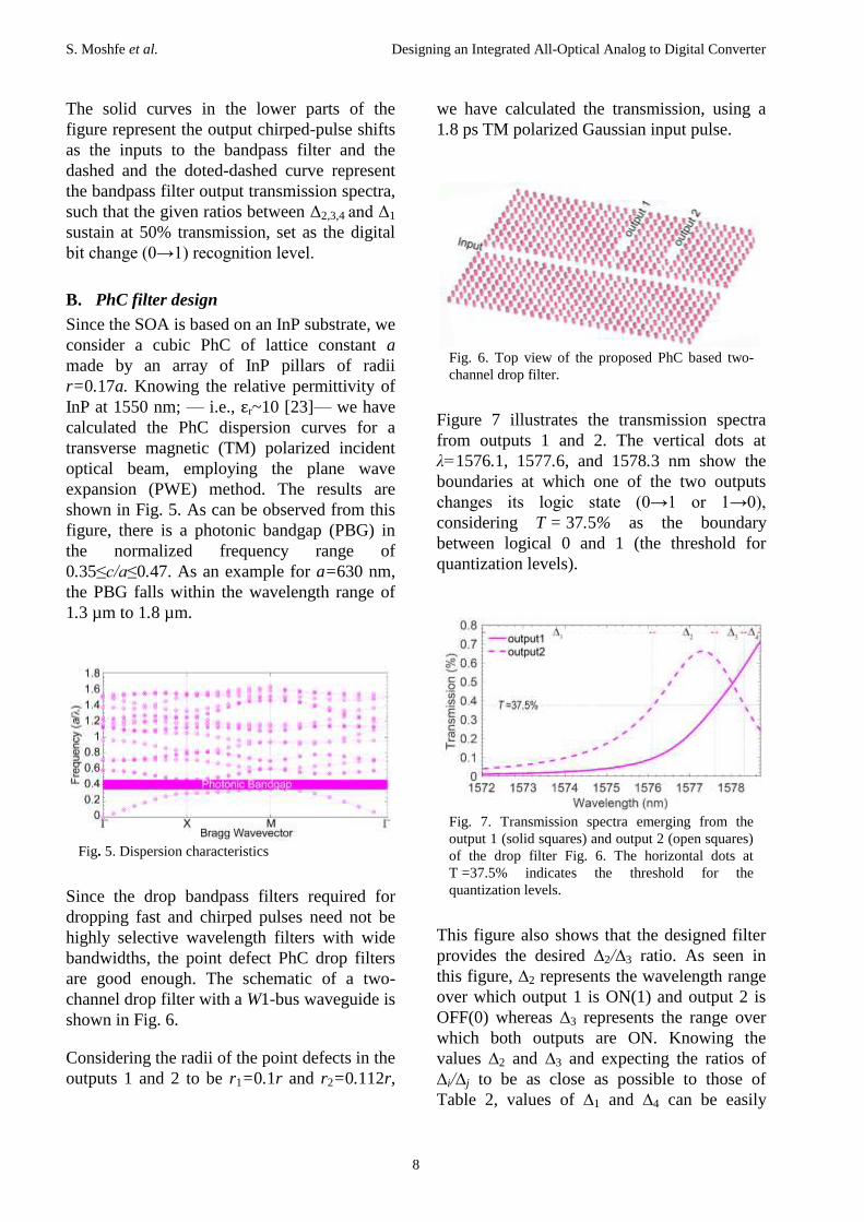
Figure 4 illustrates how this compensation can
be applied schematically.
Fig. 4. Optical quantization by PhC filters.
S. Moshfe et al. Designing an Integrated All-Optical Analog to Digital Converter
8
The solid curves in the lower parts of the
figure represent the output chirped-pulse shifts
as the inputs to the bandpass filter and the
dashed and the doted-dashed curve represent
the bandpass filter output transmission spectra,
such that the given ratios between Δ2,3,4 and Δ1
sustain at 50% transmission, set as the digital
bit change (0→1) recognition level.
B. PhC filter design
Since the SOA is based on an InP substrate, we
consider a cubic PhC of lattice constant a
made by an array of InP pillars of radii
r=0.17a. Knowing the relative permittivity of
InP at 1550 nm; — i.e., εr~10 [23]— we have
calculated the PhC dispersion curves for a
transverse magnetic (TM) polarized incident
optical beam, employing the plane wave
expansion (PWE) method. The results are
shown in Fig. 5. As can be observed from this
figure, there is a photonic bandgap (PBG) in
the normalized frequency range of
0.35≤c/a≤0.47. As an example for a=630 nm,
the PBG falls within the wavelength range of
1.3 µm to 1.8 µm.
Fig. 5. Dispersion characteristics
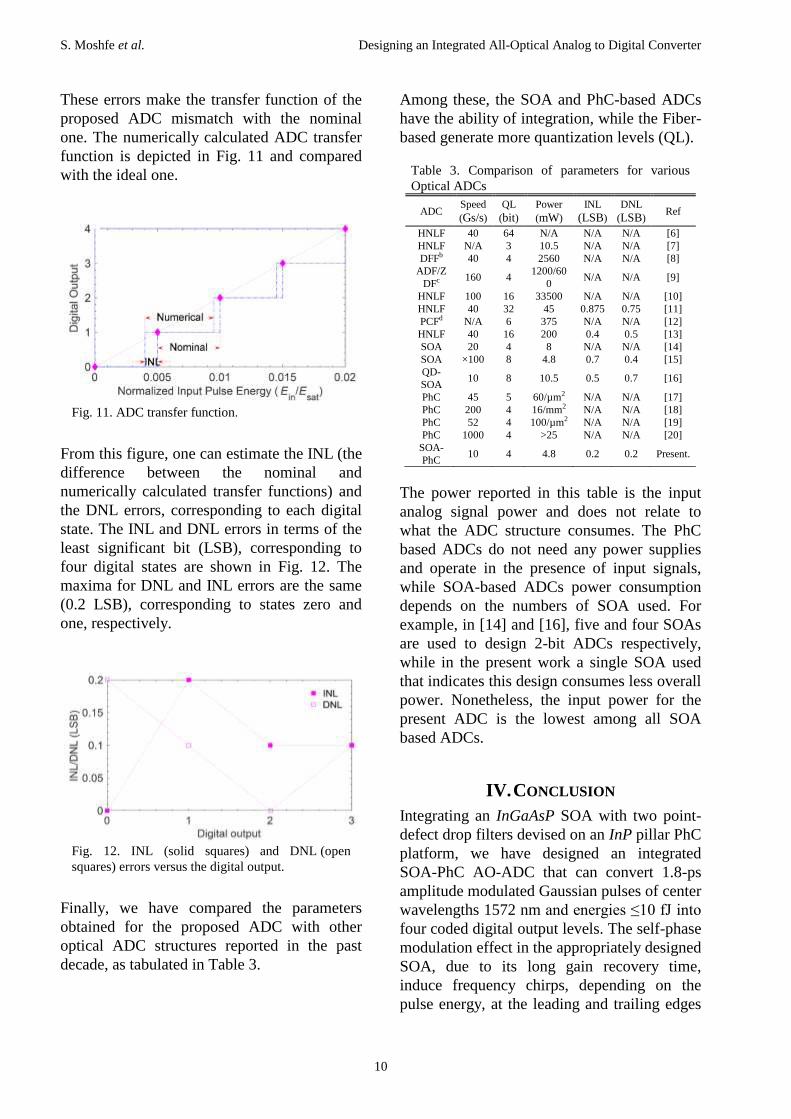
Since the drop bandpass filters required for
dropping fast and chirped pulses need not be
highly selective wavelength filters with wide
bandwidths, the point defect PhC drop filters
are good enough. The schematic of a two-
channel drop filter with a W1-bus waveguide is
shown in Fig. 6.
Considering the radii of the point defects in the
outputs 1 and 2 to be r1=0.1r and r2=0.112r,
we have calculated the transmission, using a
1.8 ps TM polarized Gaussian input pulse.
Fig. 6. Top view of the proposed PhC based two-
channel drop filter.
Figure 7 illustrates the transmission spectra
from outputs 1 and 2. The vertical dots at
λ=1576.1, 1577.6, and 1578.3 nm show the
boundaries at which one of the two outputs
changes its logic state (0→1 or 1→0),
considering T = 37.5% as the boundary
between logical 0 and 1 (the threshold for
quantization levels).
Fig. 7. Transmission spectra emerging from the
output 1 (solid squares) and output 2 (open squares)
of the drop filter Fig. 6. The horizontal dots at
T =37.5% indicates the threshold for the
quantization levels.
This figure also shows that the designed filter
provides the desired ∆2/∆3 ratio. As seen in
this figure, ∆2 represents the wavelength range
over which output 1 is ON(1) and output 2 is
OFF(0) whereas ∆3 represents the range over
which both outputs are ON. Knowing the
values ∆2 and ∆3 and expecting the ratios of
∆i/∆j to be as close as possible to those of
Table 2, values of ∆1 and ∆4 can be easily
International Journal of Optics and Photonics (IJOP) Vol. 14, No. 1, Winter-Spring, 2020
9
determined. Notice, the transmission spectra
are depicted only over a wavelength range that
equals the sum of the four ∆i values.
According to the value of ΣΔi~6.7 nm, this
design is capable of properly coding pulses of
2-nm bandwidths (Fig 3.b).
C. ADC output
Considering 1.8 ps Gaussian pulses of 1572
nm center wavelengths with different energies
launched into the designed ADC input, we
have calculated the wavelength shifts
experienced by the ADC output, while
neglecting the coupling loss between SOA and
PhC filter. The wavelength shift versus the
normalized energy is illustrated in Fig. 8.
Fig. 8. Wavelength shift exhibited by the ADC
output versus the normalized energy of 1.8-ps
Gaussian input pulse with 1572 nm center
wavelength.
This figure shows that redshifts obtained for
the pulses whose normalized input energies are
Ein/Esat=0.005, 0.01, 0.015, and 0.02 are the
desired shifts that we have aimed for.
Launching four chains of 1.8-ps Gaussian
pulses with the same center wavelength
(𝛌=1572 nm) but different energies
(Ein/Esat=0.00125, 0.00625, 0.0125, and 0.02)
four digital state of the ADC output is
examined. The simulation results show that the
wavelength shifts incurred on the input pulses
of given energies, by the SOA, coincide those
of Fig. 8, resulting in four different pulses with
center wavelengths of 𝛌=1573.95, 1576.83,
1578.08, and 1578.7 nm. Then, the PhC filter
outputs code these four pulses digitally as
desired. The time responses of the PhC filter
outputs are illustrated in Fig.9, showing the
four digital states 00, 01, 11, and 10,
considering the 37.5% transmission level
(horizontal dots) as the threshold.
Fig. 9. Time response of the filters (a) output 1 and
(b) output 2, depicting the four digital states 00, 01,
11, and 10, considering 37.5% transmission level
(horizontal dots) as the threshold.
As can be seen from this figure, the filter
response time is shorter than the repetition
rate; but the gain recovery time of the SOA is a
limiting parameter. Using the data given in
Table 1, the transparency current is I0=47 mA.
The corresponding gain recovery time is found
to be ~100 ps (see Fig. 10). In other words, the
proposed AO-ADC sampling rate is ~10Gs/s.
Fig. 10. Gain recovery of the SOA.
The threshold we defined for the filters, the
differences between the ratios of Δi/Δj in the
PhC filters and the SOA wavelength shift are
the sources of errors in the proposed ADC.
S. Moshfe et al. Designing an Integrated All-Optical Analog to Digital Converter
10
These errors make the transfer function of the
proposed ADC mismatch with the nominal
one. The numerically calculated ADC transfer
function is depicted in Fig. 11 and compared
with the ideal one.
Fig. 11. ADC transfer function.
From this figure, one can estimate the INL (the
difference between the nominal and
numerically calculated transfer functions) and
the DNL errors, corresponding to each digital
state. The INL and DNL errors in terms of the
least significant bit (LSB), corresponding to
four digital states are shown in Fig. 12. The
maxima for DNL and INL errors are the same
(0.2 LSB), corresponding to states zero and
one, respectively.
Fig. 12. INL (solid squares) and DNL (open
squares) errors versus the digital output.
Finally, we have compared the parameters
obtained for the proposed ADC with other
optical ADC structures reported in the past
decade, as tabulated in Table 3.
Among these, the SOA and PhC-based ADCs
have the ability of integration, while the Fiber-
based generate more quantization levels (QL).
Table 3. Comparison of parameters for various
Optical ADCs
ADC Speed
(Gs/s)
QL
(bit)
Power
(mW)
INL
(LSB)
DNL
(LSB) Ref
HNLF 40 64 N/A N/A N/A [6]
HNLF N/A 3 10.5 N/A N/A [7]
DFFb 40 4 2560 N/A N/A [8]
ADF/Z
DFc 160 4
1200/60
0 N/A N/A [9]
HNLF 100 16 33500 N/A N/A [10]
HNLF 40 32 45 0.875 0.75 [11]
PCFd N/A 6 375 N/A N/A [12]
HNLF 40 16 200 0.4 0.5 [13]
SOA 20 4 8 N/A N/A [14]
SOA ×100 8 4.8 0.7 0.4 [15]
QD-
SOA 10 8 10.5 0.5 0.7 [16]
PhC 45 5 60/µm2 N/A N/A [17]
PhC 200 4 16/mm2 N/A N/A [18]
PhC 52 4 100/µm2 N/A N/A [19]
PhC 1000 4 >25 N/A N/A [20]
SOA-
PhC 10 4 4.8 0.2 0.2 Present.
The power reported in this table is the input
analog signal power and does not relate to
what the ADC structure consumes. The PhC
based ADCs do not need any power supplies
and operate in the presence of input signals,
while SOA-based ADCs power consumption
depends on the numbers of SOA used. For
example, in [14] and [16], five and four SOAs
are used to design 2-bit ADCs respectively,
while in the present work a single SOA used
that indicates this design consumes less overall
power. Nonetheless, the input power for the
present ADC is the lowest among all SOA
based ADCs.
IV. CONCLUSION
Integrating an InGaAsP SOA with two point-
defect drop filters devised on an InP pillar PhC
platform, we have designed an integrated
SOA-PhC AO-ADC that can convert 1.8-ps
amplitude modulated Gaussian pulses of center
wavelengths 1572 nm and energies ≤10 fJ into
four coded digital output levels. The self-phase
modulation effect in the appropriately designed
SOA, due to its long gain recovery time,
induce frequency chirps, depending on the
pulse energy, at the leading and trailing edges
International Journal of Optics and Photonics (IJOP) Vol. 14, No. 1, Winter-Spring, 2020
11
of the signal passing through it. The two
bandpass PhC filters are appropriately
designed to digitize and code the shifted
signals, leading to the Gray code (00, 01, 11,
and 10). Designing appropriate filters
according to the range of redshifts, we have
obtained the key element of this structure to be
as linear as it can. The proposed integrated
AO-ADC can be used in a photonic network
like an all-optical quaternary ASK to OOK
modulation format converter or an all-optical
BEM system. The proposed design can be
developed to have more quantization levels as
a new generation of integrated AO-ADCs.
REFERENCES
[1] H. F. Taylor, H. F. M. J. Taylor, and P. W.
Bauer, “Electro-optic analog-to-digital
conversion using channel waveguide
modulators,” Appl. Phys. Lett. Vol. 32, pp.
559-561, 1978.
[2] L. Y. Nathawad, R. Urata, B. A. Wooley, and
D. A. B. Miller, “A 40-GHz-bandwidth, 4-bit,
time-interleaved A/D converter using
photoconductive sampling,” IEEE J. Solid-
State Circuits, Vol. 38, pp. 2021-2030, 2003.
[3] S. Yang, C. Wang, H. Chi, X. Zhang,
S. Zheng, X. Jin, and J. Yao, “Photonic
analog-to-digital converter using Mach-
Zehnder modulators having identical half-
wave voltages with improved bit resolution,”
Appl. Opt. Vol. 48, pp. 4458-4467, 2009.
[4] J.-M. Jeong and M. E. Marhic, “All-optical
analog-to-digital conversion implemented by a
nonlinear fiber interferometer,” Opt.
Commun. Vol. 91, pp. 115-122, 1992.
[5] L. Brozozowski and E. H. Sargent, “All-
optical analog-to-digital converters, hard
limiters, and logic gates,” J. Lightw. Technol.
Vol. 19, pp. 114-119, 2001.
[6] Ch. Xu and Xi. Liu, “Photonic analog-to-
digital converter using Soliton self-frequency
shift and interleaving spectral filters,” Opt.
Lett. Vol. 28, pp. 986-988, 2003.
[7] T. Nishitani, T. Konishi, and K. Itoh,
“Integration of proposed all-optical analog-to-
digital converter using self-frequency shifting
in fiber and a pulse-shaping technique,” Opt.
Rev. Vol. 12, pp. 237-241, 2005.
[8] Sh-i. Oda and A. Maruta, “A novel
quantization scheme by slicing
supercontinuum spectrum for all-optical
analog-to-digital conversion,” IEEE Photon.
Technol. Lett. Vol. 17, pp. 465-467, 2005.
[9] Sh. Oda and A. Maruta, “Two-bit all-optical
analog-to-digital conversion by filtering
broadened and split spectrum induced by
Soliton effects on self-phase modulation in
fiber,” IEEE J. Sel. Top. Quantum Electron.
Vol. 12, pp. 307-314, 2006.
[10] T. Nishitani, T. Konishi, and K. Itoh,
“Resolution improvement of all-optical
analog-to-digital conversion employing self-
frequency shift and self-phase-modulation
induced spectral compression,” IEEE J. Sel.
Top. Quantum Electron. Vol. 14, pp. 724-732,
2008.
[11] T. Konishi, K. Takahashi, H. Matsui, T.
Satoh, and K. Itoh, “Five-bit parallel operation
of optical quantization and coding for
photonic analog-to-digital conversion,” Opt.
Exp. Vol. 19, pp. 16106-16114, 2011.
[12] K. Zhe, Y. Jin-Hui, L. Sha, X. Song-Lin, Y.
Bin-Bin, S. Xin-Zhu, and Y. Chong-Xiu, “Six-
bit all optical quantization using photonic
crystal fiber with pre-chirped spectral
compression techniques,” Chin. Phys. Vol. B
22, pp. 114211 (1-5), 2013.
[13] T. Nagashima, M. Hasegawa, and T. Konishi,
“40GSampl/s all-optical analog to digital with
resolution degradation prevention,” IEEE
Photon. Technol. Lett. Vol. 29, pp. 74-77,
2017.
[14] M. Scaffardi, E, Lazzeri, F. Fresi, L. Poti L,
and A. Bogoni. “Analog-to-Digital
Conversion based on Modular Blocks
Exploiting Cross-gain Modulation in
Semiconductor Amplifiers,” IEEE Photon.
Technol. Lett. Vol. 21, pp. 540-542, 2009.
[15] H. Wen, H. Wang, and Y. Ji, “All-optical
quantization and coding scheme for ultra-fast
analog-to-digital conversion exploiting
polarization switches based on nonlinear
polarization rotation in semiconductor optical
amplifiers,” Opt. Commun. Vol. 285, pp.
3877-3885, 2012.
S. Moshfe et al. Designing an Integrated All-Optical Analog to Digital Converter
12
[16] H. Hoshino, T. Okada, and M. Matsuura,
“Photonic analog-to-digital conversion using a
red frequency chirp in a semiconductor optical
amplifier,” Opt. Lett. Vol. 43, pp. 2272-2275,
2018.
[17] B. Yousefi, M. K. Moravvej-Farshi, and N.
Granpayeh, “Two-bit all-optical analog-to-
digital converter based on nonlinear Kerr
effect in 2D photonic crystals,” Opt. Commun.
Vol. 285, pp. 3228-3223, 2012.
[18] F. Mehdizadeh, M. Soroosh, H. Alipour-
Banaei, and E. Farshidi, “All Optical 2-bit
Analog to Digital Converter Using Photonic
Crystal Based Cavities,” Opt. Quantum
Electron. Vol. 49, pp. 1-11, 2017.
[19] F. Mehdizadeh, M. Soroosh, H. Alipour-
Banaei, and E. Farshidi, “A novel proposal for
all optical analog-to-digital converter based on
photonic crystal structures,” IEEE Photon. J.
Vol. 9, pp. 4700311 (1-12), 2017.
[20] D. Jafari, T. Nurmohammadi, M. J. Asadi, and
K. Abbasian “All-Optical Analog-to-Digital
Converter based on Kerr Effect in Photonic
Crystal,” Opt. Laser Technol. Vol. 101, pp.
138-143, 2018.
[21] G. P. Agrawal and N. A. Olsson, “Self-phase
modulation and spectral broadening of optical
pulses in semiconductor laser amplifiers,”
IEEE J. Quantum Electron. Vol. 25, pp. 2297-
2306, 1989.
[22] P. P. Baveja, D. N. Maywar, A. M. Kaplan,
and G. P. Agrawal, “Spectral broadening in
ultrafast semiconductor optical amplifiers
induced by gain dynamics and self-phase
modulation,” Opt. Lett. Vol. 35, 294-296
2010.
[23] M. Razaghi, V. Ahmadi, and M. J. Connely,
“Comprehensive finite-difference time-
dependent beam propagation model of
counterpropagating picosecond pulses in a
semiconductor optical amplifier,” J. Lightw.
Technol. Vol. 27, pp. 3162-3174, 2009.
[24] M. J. Connely, “Wideband semiconductor
optical amplifier steady-state numerical
model,” IEEE J. Quantum Electron. Vol. 37,
pp. 349-447, 2001.
[25] P. Baveja, D. N. Maywar, and G. P. Agrawal.
“Interband Four-Wave Mixing in
Semiconductor Optical Amplifiers with ASE-
Enhanced Gain Recovery,” IEEE J. Selec.
Topics Quantum Electron. Vol. 18, pp. 899-
908, 2012.
Sajjad Moshfe is currently a Ph.D. candidate,
working on his dissertation at the Department
of Electrical Engineering, Science and research
branch, Islamic Azad University, Tehran, Iran.
M. Kazem Moravvej-Farshi received the
B.Sc. and the M.A. degrees in physics from
Sharif University of Technology (SUT),
Tehran, Iran, in 1976, and the University of
Southern California (USC), Los Angeles,
California, in 1978, respectively, the M.Sc.
and the Ph.D degrees in electronics from the
University of California at Santa Barbara
(UCSB), in 1980, and the University of New
South Wales (UNSW), Sydney, Australia, in
1987, respectively. From 1980 to 1984, he was
a member of research staff with the Division of
Microwave, Iran Telecommunication Research
Center (ITRC). He joined Tarbiat Modares
University (TMU) in 1987, where he is a
Professor of Electronics and the head of the
Nano Plasmo-Photonics research group.
Professor MK Moravvej-Farshi was elected as
one of the two most prominent professors of
2002 in the field of electrical engineering,
nationwide.
Professor Moravvej Farshi is one of the
founding members of the Optics and Photonics
Society of Iran (OPSI) and is currently serving
as the president of OPSI (2016-2019). He is a
Senior Member of the Optical Society of
International Journal of Optics and Photonics (IJOP) Vol. 14, No. 1, Winter-Spring, 2020
13
America (OSA) and also IEEE Photonics and
Electron Device Societies.
Kambiz Abedi was born in Ahar, Iran, in
1970. He received the B.Sc. degree from the
University of Tehran, Tehran, Iran, in 1992,
the M.Sc. degree from Iran University of
Science and Technology, Tehran, in 1995, and
the Ph.D. degree from Tarbiat Modares
University, Tehran, in 2008, all in electrical
engineering. He is currently an Associate
Professor at Shahid Beheshti University,
Tehran, Iran. His current research interests
include design, circuit modeling, and
numerical simulation of optoelectronic
devices, semiconductor lasers, optical
modulators, optical amplifiers, detectors,
plasmonic-photonic devices, MOEMS devices,
slow light, and photonic crystals.

S. Moshfe et al. Designing an Integrated All-Optical Analog to Digital Converter
14
THIS PAGE IS INTENTIONALLY LEFT BLANK.