design and fabrication of toroidal inductors for … · design and fabrication of toroidal...
TRANSCRIPT

DESIGN AND FABRICATION OF TOROIDAL
INDUCTORS FOR MIXED SIGNAL
PACKAGING
by
Jayanthi Suryanarayanan
A thesis submitted to the Graduate Faculty ofNorth Carolina State University
in partial fulfillment of therequirements for the Degree of
Master of Science
Electrical Engineering
Raleigh
December 2002
APPROVED BY:
Chair of Advisory Committee

ABSTRACT
JAYANTHI SURYANARAYANAN. Design and Fabrication of Toroidal Inductorsfor Mixed Signal Packaging. (Under the direction of Dr.Michael B. Steer.)
The demand for efficient, lightweight consumer products created the need for minia-
turization of passive components especially inductors which are some of the bulkiest
parts of an integrated system. The purpose of the work described here was to study
toroidal inductor structures since they were compact and self-shielding. Toroidal
inductors were modeled using a commercial electromagnetic simulator. The results
show that these structures have good characteristics in terms of inductance, quality
factor and area. Three different structures are fabricated and experimentally charac-
terized using the HP Vector Network Analyzer. We also make several observations
about the effect of the placement of each pair of top and bottom metal strips with
respect to each other on the flux linkage and hence, the inductance and quality factor
of the inductor.

ii
DEDICATION
I dedicate this thesis to my parents for always being there for me and
supporting me in everything I do.

iii
BIOGRAPHY
Jayanthi Suryanarayanan was born in Tanjore, India in 1978. She grew up in
Bombay, where she also got her Bachelors in Electronics Engineering from Bombay
University in 2000. After working for a year as Systems engineer in Wipro Ericsson,
she joined NC State in Fall 2001 for the Masters program in Electrical Engineering.

iv
ACKNOWLEDGEMENTS
I take this opportunity to thank all those people who offered me their greatest support
in completing my Masters here at North Carolina State University.
I would first like to thank my advisor, Professor Michael Steer for his support
and guidance in completing my graduate studies and research work. He has been
an excellent guide and the passion with which he works is truly impressive. I have
thoroughly enjoyed the learning experience this past year and I am glad I got the
opportunity to work with him. I would also like to thank Dr. Douglas Barlage
and Dr. Paul Franzon for serving on my advisory committee and for their valuable
suggestions.
I also take this opportunity to thank everybody who helped me in every way in
completing this thesis. The list is long but I’ll name them anyway. I have to thank
Jayesh Nath, Steve Lipa and Mark Buff for helping me so much in completing my
thesis. I specially thank Keyoor Gosalia for making those structures so patiently. I
could not have done it without his skill and effort. Thanks to Sonali, Rachana and
Aditya for all the necessary diversions and good lunch breaks.
My parents deserve the biggest share in my success, and I thank them for having
faith in me and always stressing on the importance of education. Thanks Mom for
those long phone calls. Thanks Dad for everything. You are the reason I am here.

v
Contents
List of Figures vi
1 Introduction 11.1 Background . . . . . . . . . . . . . . . . . . . . . . . . . . . . . . . . 11.2 Motivation . . . . . . . . . . . . . . . . . . . . . . . . . . . . . . . . . 21.3 Organization of Thesis . . . . . . . . . . . . . . . . . . . . . . . . . . 2
2 Literature Review 32.1 Classic Model of an Inductor . . . . . . . . . . . . . . . . . . . . . . . 32.2 Comparison of Inductors Fabricated in Integrated Systems . . . . . . 7
3 Toroidal Inductor 123.1 Introduction . . . . . . . . . . . . . . . . . . . . . . . . . . . . . . . . 123.2 Theory . . . . . . . . . . . . . . . . . . . . . . . . . . . . . . . . . . . 123.3 Analysis . . . . . . . . . . . . . . . . . . . . . . . . . . . . . . . . . . 143.4 Modeling the Inductor . . . . . . . . . . . . . . . . . . . . . . . . . . 173.5 Summary . . . . . . . . . . . . . . . . . . . . . . . . . . . . . . . . . 18
4 Results 194.1 Introduction . . . . . . . . . . . . . . . . . . . . . . . . . . . . . . . . 194.2 Design goals . . . . . . . . . . . . . . . . . . . . . . . . . . . . . . . . 194.3 Simulations . . . . . . . . . . . . . . . . . . . . . . . . . . . . . . . . 204.4 Calibration and Measurements . . . . . . . . . . . . . . . . . . . . . . 34
5 Conclusions 435.1 Conclusions . . . . . . . . . . . . . . . . . . . . . . . . . . . . . . . . 43
Bibliography 45

vi
List of Figures
2.1 Distributed capacitance and series resistance in the inductor. . . . . 32.2 Equivalent circuit model of an inductor coil at high frequencies. . . . 42.3 Frequency response of the impedance of an ideal inductor and a prac-
tical inductor. . . . . . . . . . . . . . . . . . . . . . . . . . . . . . . 52.4 Change in Q factor with frequency . . . . . . . . . . . . . . . . . . . 62.5 An on-chip spiral inductor. . . . . . . . . . . . . . . . . . . . . . . . 72.6 Solenoid-type inductor . . . . . . . . . . . . . . . . . . . . . . . . . . 11
3.1 Toroidal inductor . . . . . . . . . . . . . . . . . . . . . . . . . . . . . 133.2 Toroidal inductor and magnetic flux lines . . . . . . . . . . . . . . . 133.3 Toroid-type inductor structure as simulated on HFSS. . . . . . . . . 153.4 Equivalent circuit model of an inductor coil at high frequencies. . . . 153.5 One port network model of the inductor. . . . . . . . . . . . . . . . 18
4.1 Isometric view of the toroidal inductor with unequal angles betweeneach pair of top and bottom metal strips. . . . . . . . . . . . . . . . 20
4.2 Another isometric view of the toroidal inductor with a different coilgeometry. . . . . . . . . . . . . . . . . . . . . . . . . . . . . . . . . . 21
4.3 Inductance with the radiation boundary condition. . . . . . . . . . . 224.4 Q factor with the radiation boundary condition. . . . . . . . . . . . 234.5 S11 magnitude with the radiation boundary condition. . . . . . . . . 244.6 S11 phase with the radiation boundary condition. . . . . . . . . . . . 254.7 Smith chart showing the inductive nature of the structure from 100 MHz
to 1 GHz for radiation boundary condition. . . . . . . . . . . . . . . 264.8 Plot of magnetic field in the XY plane for radiate boundary condition. 274.9 Inductance with the radiation boundary condition. . . . . . . . . . . 284.10 Q factor with the radiation boundary condition. . . . . . . . . . . . 294.11 S11 magnitude with the radiation boundary condition. . . . . . . . . 304.12 S11 phase with the radiation boundary condition. . . . . . . . . . . . 314.13 Smith chart showing the inductive nature of the structure from 100 MHz
to 1 GHz for radiation boundary condition. . . . . . . . . . . . . . . 32

vii
4.14 Plot of magnetic field in the XY plane for radiate boundary condition. 334.15 A snapshot of the 40A-GSG-1250-P Picoprobe. . . . . . . . . . . . . 354.16 Fabricated short, open and load structures. . . . . . . . . . . . . . . 354.17 Top view of the toroidal structure with approximately equal angles
between each pair of top and bottom metal strips. . . . . . . . . . . 364.18 Bottom view of the toroidal structure with approximately equal angles
between each pair of top and bottom metal strips. . . . . . . . . . . 374.19 Top view of the second toroidal structure. . . . . . . . . . . . . . . . 374.20 Bottom view of the second toroidal structure. . . . . . . . . . . . . . 384.21 Smith Chart showing measured and simulated S11 for the first struc-
ture. . . . . . . . . . . . . . . . . . . . . . . . . . . . . . . . . . . . . 394.22 Comparison of the measured and simulated inductance values for the
first toroidal inductor structure. . . . . . . . . . . . . . . . . . . . . 404.23 Comparison of the measured and simulated quality factor values for
the first toroidal inductor structure. . . . . . . . . . . . . . . . . . . 404.24 Smith Chart showing measured and simulated S11 for the second struc-
ture. . . . . . . . . . . . . . . . . . . . . . . . . . . . . . . . . . . . . 414.25 Comparison of the measured and simulated inductance values for the
third toroidal inductor structure. . . . . . . . . . . . . . . . . . . . . 424.26 Comparison of the measured and simulated quality factor values for
the third toroidal inductor structure. . . . . . . . . . . . . . . . . . . 42

1
Chapter 1
Introduction
1.1 Background
There has been a large demand for passive components for consumer products like
pagers and cellular phones leading to a lot of work to improve passive component
fabrication and packaging. One of the main uses of inductors is in transistor biasing
networks, for instance as RF coils to short circuit the device to DC voltage conditions.
One of the major issues in passive component fabrication has been the fabrica-
tion of three-dimensional inductors on silicon and in mixed signal package, and their
miniaturization. The miniaturization technology of inductors is much less advanced
compared to other passive components (e.g. resistors and capacitors), greatly limiting
the integration of electromagnetic devices.
Inductors, in general, occupy a lot of area on the chip since large magnetic cross
sectional areas are required to obtain good inductance and Q-factor. This obviously
affects any attempts at miniaturization. There is a major attempt to take the inductor
or a huge portion of it off-chip and into the package.
In general, planar spiral inductors are fabricated in integrated circuits, the spiral
inductor being the dominant choice since it is a planar inductor and hence easy to
fabricate using two dimensional techniques. In integrated systems it is difficult to
achieve high Q and high inductance partly due to the geometry of the spiral inductor
and partly due to the finite conductivity of the silicon substrate on which the inductor

2
is fabricated.
1.2 Motivation
The issues we are trying to address when fabricating integrated inductors are max-
imizing Q, maximizing inductance, increasing the self-resonant frequency, reducing
the area occupied by the inductor and making them mechanically robust. The entire
motivation behind this research has been trying to address these issues especially in
trying to make the inductor more compact, at the same time, offering much higher
inductance than the spiral or solenoid inductors which are currently the popular in-
ductors used in integrated systems. This would lead to smaller, lighter, more efficient
components being used in consumer products.
1.3 Organization of Thesis
Chapter 2 is a literature review of the inductor, the types of inductors fabricated
in integrated systems and the issues involved in fabrication and miniaturization. In
Chapter 3, the working and analysis of the toroidal inductor is presented. Chap-
ter 4 describes the simulations and experiments performed to realize the toroidal
inductor structure and the results obtained from simulations done using HFSS and
measurements made on fabricated structures. Chapter 5 presents the conclusions and
describes future work.

3
Chapter 2
Literature Review
2.1 Classic Model of an Inductor
An inductor is basically a wire coiled in such a way as to increase the magnetic flux
linkage between the turns of the coil. This increases the self-inductance of the wire
beyond what it would have been without flux linkage.
An ideal inductor is characterized by a purely reactive impedance (Z = jXL)
which is proportional to the inductance only. The phase of the signal across the ideal
inductor would always be +90 degrees out of phase with the applied voltage and there
would be no effect of DC current bias on its behavior.
Figure 2.1 shows what the inductor coil looks like at RF frequencies. The equiv-
Cd
Rd
Figure 2.1: Distributed capacitance and series resistance in the inductor.

4
SR L
CS
Figure 2.2: Equivalent circuit model of an inductor coil at high frequencies.
alent circuit model of the inductor is shown in Figure 3.4.
Since the windings are adjacently positioned a minute voltage drop occurs between
adjacent turns giving rise to a parasitic capacitance effect. This effect is called the
d istributed capacitance Cd. The parasitic shunt capacitance Cs and the series resis-
tance Rs represent composite effects of distributed capacitance Cd and resistance Rd
respectively in the inductor coil as shown in Figure 3.4. When circuits are comparable
in size to the wavelength, effects are distributed rather than lumped and the electric
energy storage in parts of a primarily inductive element or the magnetic energy stor-
age in parts of a primarily capacitive element becomes important. In the present
case there is electric field (capacitive) coupling between the turns of the inductor. A
good way to represent this effect is to add a capacitive element between each pair of
adjacent turns. At high frequencies the effect of these capacitors is to bypass some
of the turns so that not all turns have the same current.
So in a real inductor the distributed capacitance Cd affects the reactance of the
inductor. Initially, at lower frequencies, the inductor’s reactance parallels that of an
ideal inductor. However the reactance deviates from the ideal curve and increases at
a much faster rate until it reaches a peak at the inductor’s self-resonant frequency
(SRF). The SRF is given by SRF = 1/2π√
LCs. As the frequency continues to in-
crease the distributed capacitance Cd becomes dominant. So the inductor’s reactance
begins to decrease with frequency, a voltage phase shift of -90 degrees is observed and

5
f0
Frequency
(Self resonant frequency)
Ideal inductor
Inductive Capacitive
Imp
edan
ce
Figure 2.3: Frequency response of the impedance of an ideal inductor and a practicalinductor.
the inductor begins to look like a capacitor. This behavior of the inductor is shown
in Figure 2.3.
Theoretically the resonance peak would occur at infinite reactance. However, due
to the series resistance of the coil, some finite impedance is seen at resonance. The
series resistance also serves to broaden the resonance peak of the impedance curve of
the coil. To characterize the impact of the series resistance the quality factor Q is
commonly used. The Q is the ratio of an inductor’s reactance to its series resistance
(Q = XL/R) and characterizes the resistive loss in the inductor. For tuning purposes,
this ratio should be as high as possible. If the coil were a perfect conductor, its Q
would be infinite and the inductor would be lossless. But since there is no perfect
conductor an inductor always has a finite Q.
At low frequencies, the Q factor is very good because the only resistance seen is
the dc resistance of the wire which is very small. But as the frequency increases, skin
6
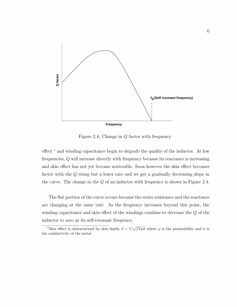
f0 (Self resonant frequency)
Frequency
Q f
acto
r
Figure 2.4: Change in Q factor with frequency
effect 1 and winding capacitance begin to degrade the quality of the inductor. At low
frequencies, Q will increase directly with frequency because its reactance is increasing
and skin effect has not yet become noticeable. Soon however the skin effect becomes
factor with the Q rising but a lower rate and we get a gradually decreasing slope in
the curve. The change in the Q of an inductor with frequency is shown in Figure 2.4.
The flat portion of the curve occurs because the series resistance and the reactance
are changing at the same rate. As the frequency increases beyond this point, the
winding capacitance and skin effect of the windings combine to decrease the Q of the
inductor to zero at its self-resonant frequency.
1Skin effect is characterized by skin depth, δ = 1/√
fπµσ where µ is the permeability and σ isthe conductivity of the metal

7
Spiral Inductor
Air Bridge
Figure 2.5: An on-chip spiral inductor.
2.2 Comparison of Inductors Fabricated in Inte-
grated Systems
Integrated inductors are typically formed on-chip or embedded in the chip package
or board. Now the three-dimensional nature of an inductor makes it difficult to
fabricate it in an IC using conventional two dimensional fabrication techniques. In
general, spiral or solenoid-type inductors are fabricated in integrated circuits, the
spiral inductor being the dominant choice since it is a planar inductor and hence
easy to fabricate using two dimensional techniques. A common type of on-chip spiral
inductor is shown in Figure 2.5. This is contrary to macro-inductor structures which
are typically solenoidal or toroidal. In integrated systems it is difficult to achieve
high Q and high inductance partly due to the geometry of the spiral inductor and
partly due to the finite conductivity of the silicon substrate on which the inductor is
fabricated. Another major issue in fabricating an on-chip inductor is that it takes up
a lot of real estate. Inductors up to 10 nH can be fabricated on-chip. Beyond this it
is better to have either the entire inductor or a majority of it off-chip as a part of the
RFIC package.
One of the major sources of loss for inductors on silicon is substrate loss due to
the finite conductivity of the substrate and the resulting current flow. These induced
8
currents follow a path under the conductors of the spiral and, just as with ground
plane eddy currents, lower the inductance achieved. Eddy currents are also excited
in the metal backing of dies or package metallization.
Most silicon substrates are at least slightly doped, usually of p-type. With heavily
doped n-type strips arranged radially from the center axis of the spiral, the eddy
currents are blocked. They achieved an increase of the Q from 5.3 to 6.0 at 3.5 GHz
and from 4.3 to 4.5 at 2.0 GHz. In the spiral inductor model, the effect was also to
reduce the shunt resistance and capacitance to the substrate.
Parasitic capacitance results in resonance of the on-chip inductance structure and
hence the frequency of operation. With GaAs (εr = 12.85) the effective permittivity
of the medium can be reduced by adding a polyimide layer (εr = 3.2) and using
metallization on top of this layer [14]. Thus, the capacitance is substantially reduced.
This is at the cost of poorer thermal management as the thermal conductivity of
polyimide is substantially lower (about 100 times) than that of GaAs, and so the
power handling capability is compromised. Coupling this with thicker metallization
to reduce resistance can result in a Q that is 50% larger and a self-resonant frequency
that is 25% higher [14].
We now return to the issue of the finite conductivity of the silicon substrate. The
inducement of charges in the silicon and the insignificant skin depth of the silicon
substrate has the effect of increasing the capacitance of an interconnect line over
silicon as the electric field lines are terminated on the substrate charges. (This effect
is in addition to the induction of eddy currents in the substrate as discussed earlier.)
Now the magnetic field lines penetrate some distance into the substrate so that the LC
product is greater than if the substrate was insulating (as with GaAs). The effect is
that the velocity of propagation along the interconnect (= 1/√
LC) is reduced, leading
to what is called the slow wave effect. This means that very small inductances can
be realized using short lengths of interconnect arranged so that fields, particularly
the magnetic field, penetrates the substrate. This effect can be adequately simulated
using planar electromagnetic simulators that allow the conductivity of media to be
specified. Simulation is necessary as the effect is a complex function of geometry
and substrate conductivity, and generalizations available for use in design are not

9
available.
The lowest loss inductors are obtained by etching away the underlying substrate
or by using insulating or very high resistivity bulk material. Loss is also reduced by
separating the planar inductor from the ground plane and additional dielectric layers
have been deposited on a chip to achieve this. Volant and Groves [15] obtained a
Q of 18 at 10 GHz with a 4 µm thick aluminum-copper spiral inductor using this
approach. When all steps have been taken then the dominant loss mechanism is
current crowding [16]. This is a particular problem with multi-turn spiral inductors
which are required to realize high inductance values. Current crowding results when
the magnetic field of one turn penetrates an adjacent trace creating eddy currents
so that current peaks on the inside edge of the victim trace (towards the center of
the spiral) and reduces on the outside edge. This constricts current and results in
higher resistance than would be predicted from skin effect and DC resistance alone
[16]. The key requirement then is that magnetic flux be confined while still achieving
flux linkage. The proposed toroidal inductor does just this.
Planar inductors are often fabricated in close proximity to each other. The cou-
pling of adjacent planar inductors depends on the separation of the inductors, shield-
ing, geometry and the resistivity of the underlying substrate. An effective measure of
shielding is to use a discontinuous guard ring [17]. This however reduces the originally
designed inductance values because of the image currents induced in the ring [18].
In summary the best that can be achieved for conventional spiral inductors on low
resistivity silicon is around 20.
The issues we are trying to address when fabricating integrated inductors are:
• Maximizing Q,
• maximizing inductance,
• increasing the self-resonant frequency and
• reducing area occupied by the inductor.
The most severe problem that degrades Q factor at high frequencies (above 500MHz)
is the I2R losses from eddy currents in the metal traces that make up the spiral induc-

10
tor. The spiral’s B-field generated by nearby turns passes perpendicularly through
the traces, setting up eddy currents and pushing currents to the trace edges. The
result is a quadratic increase in resistance with frequency with the frequency decided
by the trace width, pitch and sheet resistance. The problem is not reduced by using
traces of lower resistance either.
Fields produced by the spiral inductor penetrate the substrate and as a ground
plane is located at a relatively short distance, the eddy currents on the ground plane
reduce the inductance that would otherwise be obtained. The eddy current in the
ground conductor rotates in a direction opposite to that of the spiral itself. Conse-
quently the inductance of the image inductor in the ground is in the opposite direction
to that produced by the spiral itself, with the consequent effect that the effective total
inductance is reduced.
Since the spiral inductor requires a lead wire to connect from the inside end of
the coil to the outside a capacitance is introduced between the conductor and the
lead wire. This is one of the dominant stray capacitances of the spiral inductor and
it serves to reduce the self-resonant frequency of the inductor.
The spiral inductor takes up large two-dimensional spaces compared to other
inductor types with the same number of turns. Also the direction of flux of the spiral
inductor is perpendicular to the substrate which can cause more interference with
underlying circuitry or other vertically integrated passives.
Though the solenoid-type inductor has better electrical properties (high Q and
high inductance) and is more compact than the spiral inductor it has its problems.
These can be discussed in comparison with the toroidal inductor.
The air-core solenoidal inductor requires more number of turns than the toroidal
inductor for a given inductance. So there is more ac resistance in a solenoid compared
to the toroid which reduces its Q factor at a given frequency.
In a typical air core inductor, the magnetic flux lines linking the turns of the
inductor take the shape shown in Figure 2.6.
The air surrounding the inductor is definitely part of the magnetic-flux path.
So the solenoid tends to radiate RF signals flowing within. To reduce radiation
the inductor has to be surrounded by a bulky shield which tends to reduce available

11
Figure 2.6: Solenoid-type inductor
space and the Q of the inductor it is shielding. On the other hand a toroid completely
contains the magnetic flux within the material itself thus preventing RF signals from
radiating. Practically some minimal radiation occurs. But bulky shields are not
required surrounding the inductor.

12
Chapter 3
Toroidal Inductor
3.1 Introduction
Having explained the advantages of toroidal inductors over other types of inductors
fabricated on silicon this chapter discusses the theory behind the proposed inductor.
The inductor is also analyzed for turns of rectangular cross section.
3.2 Theory
If a long solenoid is bent into a circle and closed on itself, a toroidal coil, or toroid,
is obtained as shown in Figure 3.1. When the toroid has a uniform winding of many
turns, the magnetic lines of flux are almost entirely confined to the interior of the
winding, B being substantially zero outside. If the ratio R/r is large, one may
calculate B as though the toroid were straightened out into a solenoid.
The magnetic lines of flux produced by a current in a toroidal coil form closed
loops. Each line that passes through the entire toroid links the current N times. This
is shown in Figure 3.2. If all the lines link all the turns, the total magnetic flux linkage
Λ of the toroid is equal to the total magnetic flux ψm through the toroid times the
number of turns.
Λ = Nψm. (3.1)
The unit of flux linkage is Wbturns.

13
r
R
B
B
N turns
I
Figure 3.1: Toroidal inductor
r
R
B
B
N turns
I
Figure 3.2: Toroidal inductor and magnetic flux lines

14
Thus, the magnetic flux linkage is
Λ = Nψm = NBA = NµNI
2πRπr2 =
µN2Iπr2
2πR=
µN2r2I
2R. (3.2)
By definition the inductance L is the ratio of the total magnetic flux linkage to
the current I through the inductor.
L =Nψm
I=
Λ
I. (3.3)
This definition is satisfactory for a medium of constant permeability. Inductance has
the dimensions of magnetic flux (linkage) divided by current.
The inductance of the toroid is then
L =Λ
I=
µN2r2
2R. (3.4)
where, L = inductance of toroid, H
µ = permeability (uniform and constant) of medium inside coil, Hm−1
N = number of turns of toroid, dimensionless
r = radius of coil, m
R = mean radius of toroid, m.
At higher frequencies, when turns are relatively close together current elements
in neighboring turns will be near enough to produce nearly as much effect upon
current distribution in a given turn as the current in that turn itself. The separation
between internal and external inductance that is done at low frequencies to take into
consideration the cross section of the wire (provided it is small compared to the loop
radius r) in the expression for the internal inductance may not be possible for these
coils because a given field line may be sometimes inside and sometimes outside of the
conductor. Distributed capacitance is also an important issue at high frequencies as
explained before.
3.3 Analysis
Designing the toroidal inductor with turns of rectangular cross section
The isometric view of the toroidal inductor structure as simulated on HFSS is shown
in Figure 3.3.
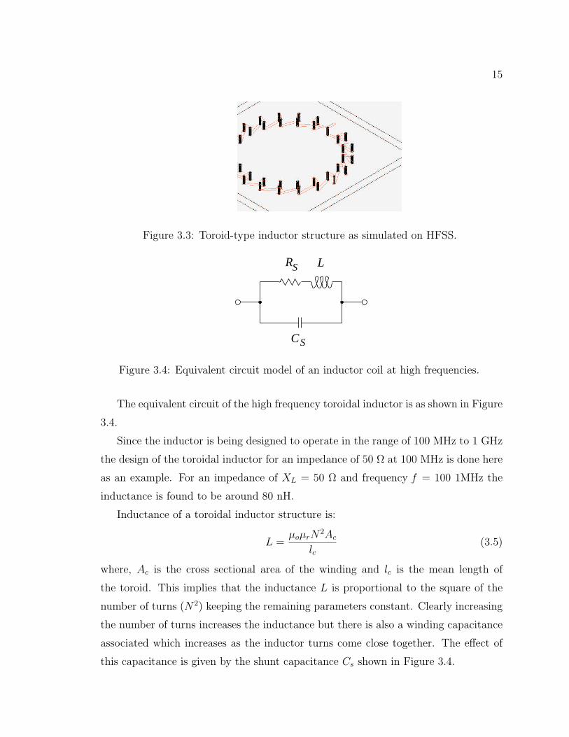
15
Figure 3.3: Toroid-type inductor structure as simulated on HFSS.
SR L
CS
Figure 3.4: Equivalent circuit model of an inductor coil at high frequencies.
The equivalent circuit of the high frequency toroidal inductor is as shown in Figure
3.4.
Since the inductor is being designed to operate in the range of 100 MHz to 1 GHz
the design of the toroidal inductor for an impedance of 50 Ω at 100 MHz is done here
as an example. For an impedance of XL = 50 Ω and frequency f = 100 1MHz the
inductance is found to be around 80 nH.
Inductance of a toroidal inductor structure is:
L =µoµrN
2Ac
lc(3.5)
where, Ac is the cross sectional area of the winding and lc is the mean length of
the toroid. This implies that the inductance L is proportional to the square of the
number of turns (N2) keeping the remaining parameters constant. Clearly increasing
the number of turns increases the inductance but there is also a winding capacitance
associated which increases as the inductor turns come close together. The effect of
this capacitance is given by the shunt capacitance Cs shown in Figure 3.4.

16
The distributed capacitance resonates out the inductance of the toroid at a par-
ticular self-resonant frequency. At this frequency, the Q of the inductor drops to
zero ideally as the impedance approaches infinity. To approximate the effect of the
capacitance Cs, the formula of an ideal parallel-plate capacitor as given in Equation
3.6 is used.
Cs = εoεrA/d (3.6)
In our case the separation d between the plates is assumed to be equal to the
distance between the turns. Therefore
d = l/N = 2πR/N (3.7)
where,
l is the length of the toroid and
R is the mean radius of the toroid. The area can be estimated as
A = 2(wc + hc )d N (3.8)
where
wc is the width of the metal strip,
hc is the height of the via,
d is the diameter of the via, and
N is the number of turns of the inductor. So it can be concluded that
Cs = εoεr[2(wc + hc)d]N2/2πR. (3.9)
For a 20 turn inductor with wc = 50 µm, hc = 250 µm and diameter of via, d = 20 µm
and assuming the dielectric constant of the substrate to be εr = 3.2 the distributed
capacitance is found to be Cs = 17.31 fF.
So the self-resonant frequency, fo of the structure is given by
fo =1
2π√
LC. (3.10)
The self-resonant frequency has to be higher than the operating frequency of the
structure so that the inductor has a band of frequencies in which it can be operated

17
before the distributed capacitance starts becoming dominant. With the calculated
values of inductance and distributed capacitance, fo is found to be 42.8 GHz.
Since the thickness of the metal is taken to be 20 microns, to compute the series
resistance Rs as a DC resistance the following formula shown in Equation 3.11 is used.
Rs = l/σCu(πd2
4) = 2πR/σCu(
πd2
4) (3.11)
where
l is the length of the toroid,
d is the diameter of the via, and
R is the mean radius of the toroid.
The mean radius R has to be found from the equation for the inductance of the toroid.
The Q factor of the inductor is given by
Q = XL/Rs = 2πfL/Rs. (3.12)
For a rectangular cross section,
L =µoµrN
2Ac
lc=
µoµrN2wchc
2πR(3.13)
For a 20 turn inductor with wc = 50 µm and hc = 250 µm the mean radius of the
toroid is found to be
R =µoµrN
2wchc
2πL(3.14)
The calculated value of R with the given values is 12.5µm. Substituting it back
in Equation 3.11 the series resistance Rs is found to be 4.3 mΩ.
At high frequencies the thickness of the metal strip need not be considered in the
formula for inductance because of skin effect which causes most of the current to be
on the surface of the metal. So it is not used to derive L.
3.4 Modeling the Inductor
As seen in Figure 3.3 due to the way in which the toroidal structure is built the
inductor is essentially modelled as a one-port network. S11 is the input reflection co-
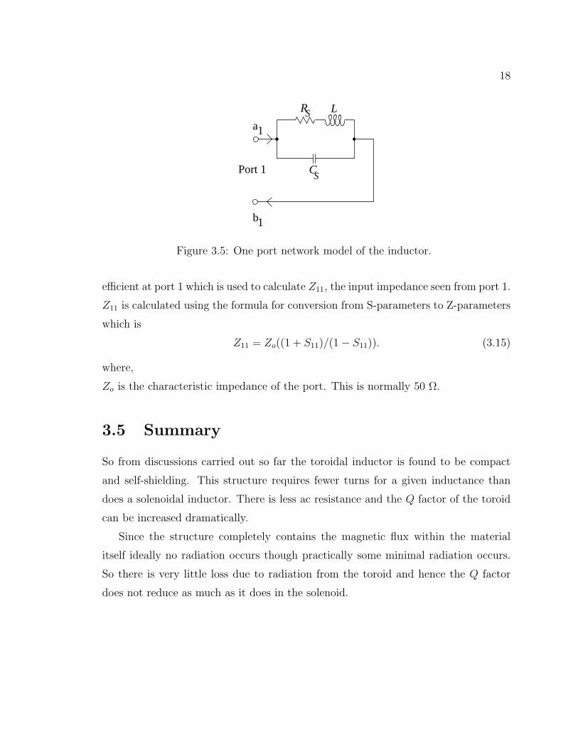
18
1b
1a
Port 1 CS
LSR
Figure 3.5: One port network model of the inductor.
efficient at port 1 which is used to calculate Z11, the input impedance seen from port 1.
Z11 is calculated using the formula for conversion from S-parameters to Z-parameters
which is
Z11 = Zo((1 + S11)/(1− S11)). (3.15)
where,
Zo is the characteristic impedance of the port. This is normally 50 Ω.
3.5 Summary
So from discussions carried out so far the toroidal inductor is found to be compact
and self-shielding. This structure requires fewer turns for a given inductance than
does a solenoidal inductor. There is less ac resistance and the Q factor of the toroid
can be increased dramatically.
Since the structure completely contains the magnetic flux within the material
itself ideally no radiation occurs though practically some minimal radiation occurs.
So there is very little loss due to radiation from the toroid and hence the Q factor
does not reduce as much as it does in the solenoid.

19
Chapter 4
Results
4.1 Introduction
This chapter describes the simulations and experiments performed to realize the
toroidal inductor structure. Comparisons are made between the results obtained
from the simulations performed using Agilent’s High Frequency Structure Simulator
and measurements taken for the two fabricated structures.
4.2 Design goals
The design goals for the toroidal inductor include
• less area occupied on the package,
• high Q,
• high inductance; almost twice that of a solenoid-type inductor, and
• high self-resonant frequency so that the inductor can be operated over a wide
band of frequencies.
The initial goal is to achieve good inductance in the range of 100 MHz to 1 GHz
with low flux leakage for a higher Q factor. In the simulation and fabrication of
the inductor the width of the metal strip at the top of the substrate is taken to be

20
Figure 4.1: Isometric view of the toroidal inductor with unequal angles between eachpair of top and bottom metal strips.
6 mm, the height of the substrate is 1.5 mm, the diameter of the via is 1.15 mm, the
thickness of the metal strip is 20 microns, the mean radius of the toroid is 10 mm,
the relative permittivity of the substrate is εr = 3.2 and the relative permeability of
the substrate is 1. The simulations have been carried out with a 20 turn toroidal
inductors of the same dimensions as above.
4.3 Simulations
The toroid was simulated using Agilent’s High Frequency Structure Simulator (HFSS).
The metal strip was modeled as a thin metal in HFSS. Two new toroidal inductor
structures were simulated with the aim of reducing flux leakage and reducing phase
reversal of magnetic flux lines. The isometric views of the two structures are shown
in Figures 4.1 and 4.2.
Figure 4.1 shows each pair of top and bottom metal strips placed at unequal angles
with respect to each other. Figure 4.2 shows another way to construct the toroidal
inductor structure.
In the simulation environment each of these structures is surrounded by an airbox
100 mm by 100 mm by 10 mm in size. In simulating these structures the airbox
is assigned a radiation boundary condition. This boundary is also referred to as an
absorbing boundary enabling you to model the surface as open. Therefore waves
radiate outward, infinitely far into space. Because of the radiation boundary, the

21
Figure 4.2: Another isometric view of the toroidal inductor with a different coilgeometry.
calculated S-parameters include the effects of radiation loss.
Now consider the structure shown in Figure 4.1. The inductance (H) and Q factor
versus frequency (Hz), magnitude and phase of S11 versus frequency (Hz) with the
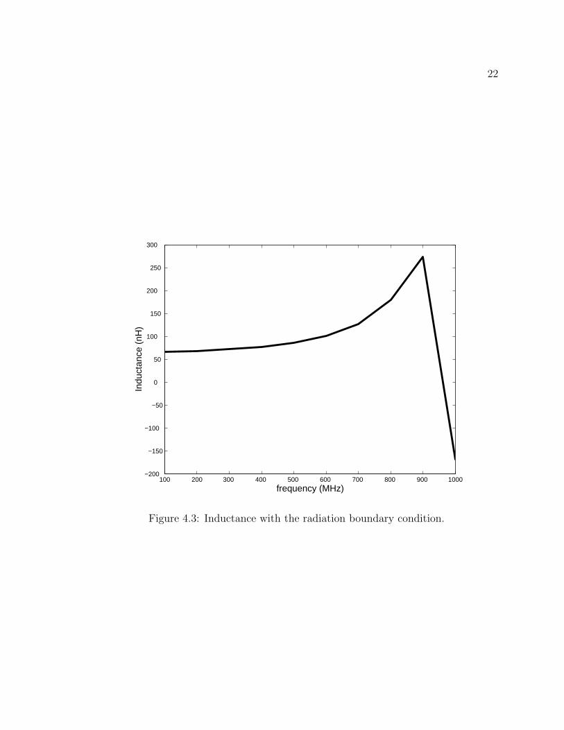
radiation boundary condition applied to the airbox are shown in Figures 4.3, 4.4, 4.5
and 4.6 respectively.
The inductance achieved with a radiation boundary is from 67 nH at 100 MHz
to 0.2 µH at resonance. The resonant frequency is 900 MHz. With the radiation
boundary condition the Q is down to around 36 which could be a more realistic figure
since there will be some radiation from the structure into space. The radiation loss is
incorporated in the Smith chart of Figure 4.7. The field plot shows that the magnetic
flux lines are essentially completely inside the turns of the toroidal inductor with little
or no radiation into space implying good flux linkage between the inductor turns.
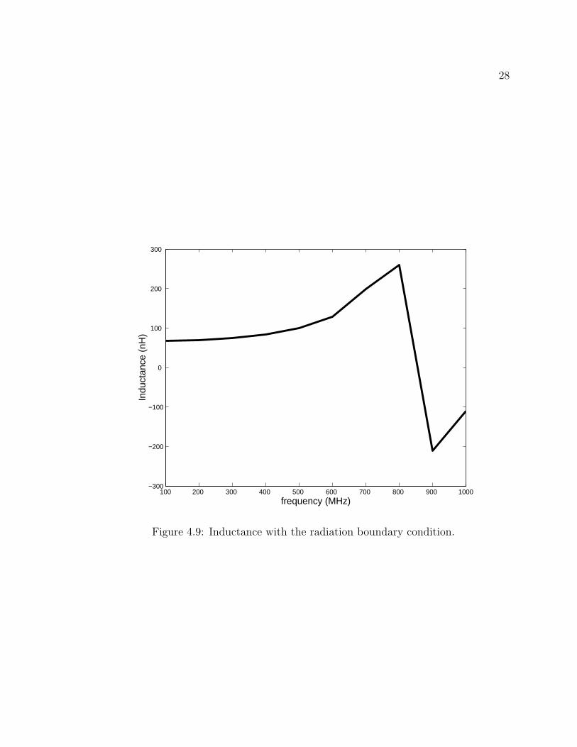
Now consider the structure shown in Figure 4.2. The inductance (H) and Q factor
versus frequency (Hz), magnitude and phase of S11 versus frequency (Hz) with the
radiation boundary condition applied to the airbox are shown in Figures 4.9, 4.10,
4.14 and 4.14 respectively.
The inductance achieved with a radiation boundary is from 67 nH at 100 MHz
to 0.26 µH at resonance. The resonant frequency is around 800 MHz. With the
radiation boundary condition the Q is down to around 33 which could be a more
realistic figure since there will be some radiation from the structure into space. The
radiation loss is incorporated in the Smith chart of Figure 4.7. The field plot shows
22
100 200 300 400 500 600 700 800 900 1000−200
−150
−100
−50
0
50
100
150
200
250
300
Indu
ctan
ce (
nH)
frequency (MHz)
Figure 4.3: Inductance with the radiation boundary condition.

23
100 200 300 400 500 600 700 800 900 1000−5
0
5
10
15
20
25
30
35
40
Q fa
ctor
frequency (MHz)
Figure 4.4: Q factor with the radiation boundary condition.

24
Figure 4.5: S11 magnitude with the radiation boundary condition.

25
Figure 4.6: S11 phase with the radiation boundary condition.

26
Figure 4.7: Smith chart showing the inductive nature of the structure from 100 MHzto 1 GHz for radiation boundary condition.

27
Figure 4.8: Plot of magnetic field in the XY plane for radiate boundary condition.
28
100 200 300 400 500 600 700 800 900 1000−300
−200
−100
0
100
200
300
Indu
ctan
ce (
nH)
frequency (MHz)
Figure 4.9: Inductance with the radiation boundary condition.

29
100 200 300 400 500 600 700 800 900 1000−5
0
5
10
15
20
25
30
35
Q fa
ctor
frequency (MHz)
Figure 4.10: Q factor with the radiation boundary condition.

30
Figure 4.11: S11 magnitude with the radiation boundary condition.

31
Figure 4.12: S11 phase with the radiation boundary condition.

32
Figure 4.13: Smith chart showing the inductive nature of the structure from 100 MHzto 1 GHz for radiation boundary condition.

33
Figure 4.14: Plot of magnetic field in the XY plane for radiate boundary condition.
34
that the magnetic flux lines are essentially completely inside the turns of the toroidal
inductor with little or no radiation into space implying good flux linkage between the
inductor turns.
Comparing the two structures we find that the inductance offered by the structure
shown in Figure 4.2 is higher than that offered by the other structure as frequency
increases implying better flux linkage. Till about 600 MHz the two structures seem
to offer the same inductance approximately. But the self-resonant frequency of the
latter structure is less than that of the first one. This could simply be the effect of
the latter structure being electrically longer than the previous one.
4.4 Calibration and Measurements
The direct measurement of the model parameters (inductance, resistance and stray
capacitance) of the toroidal inductor is difficult because of the distributed nature and
strong interaction of the parasitic effects. Typically, any of these parameters can
only be obtained from measurable parameters such as impedance, quality factor and
resonant frequency. We cannot ignore phase because of the frequency dependence
of the model. Therefore, scalar (magnitude only) measurements are not adequate.
Calibration structures are designed and fabricated on the same board as the inductor.
The measurement is done using a Model 40A probe with Ground, Signal, Ground
configuration and with 1250 microns pitch and the Vector Network Analyzer (HP
8510).
The calibration plane for the measurement of the S-parameters is at the probe
tip. Error correction of the measured S-parameters involves calibration of the cable
effects, connector mismatches, transmission line loss and phase compensation, up to
the calibration plane. The SOLT (Short Open Load Thru) calibration procedure
involves defining the standards precisely to the Network Analyzer (NA) in terms
of what are known as calibration constants and performing a user calibration. The
fabricated short and open structures are shown in Figure 4.16. The load was achieved
by connecting a 50 Ω termination directly to the Network Analyzer cable and then
performing the load calibration. The calibration structures have been fabricated in

35
Figure 4.15: A snapshot of the 40A-GSG-1250-P Picoprobe.
Figure 4.16: Fabricated short, open and load structures.
36
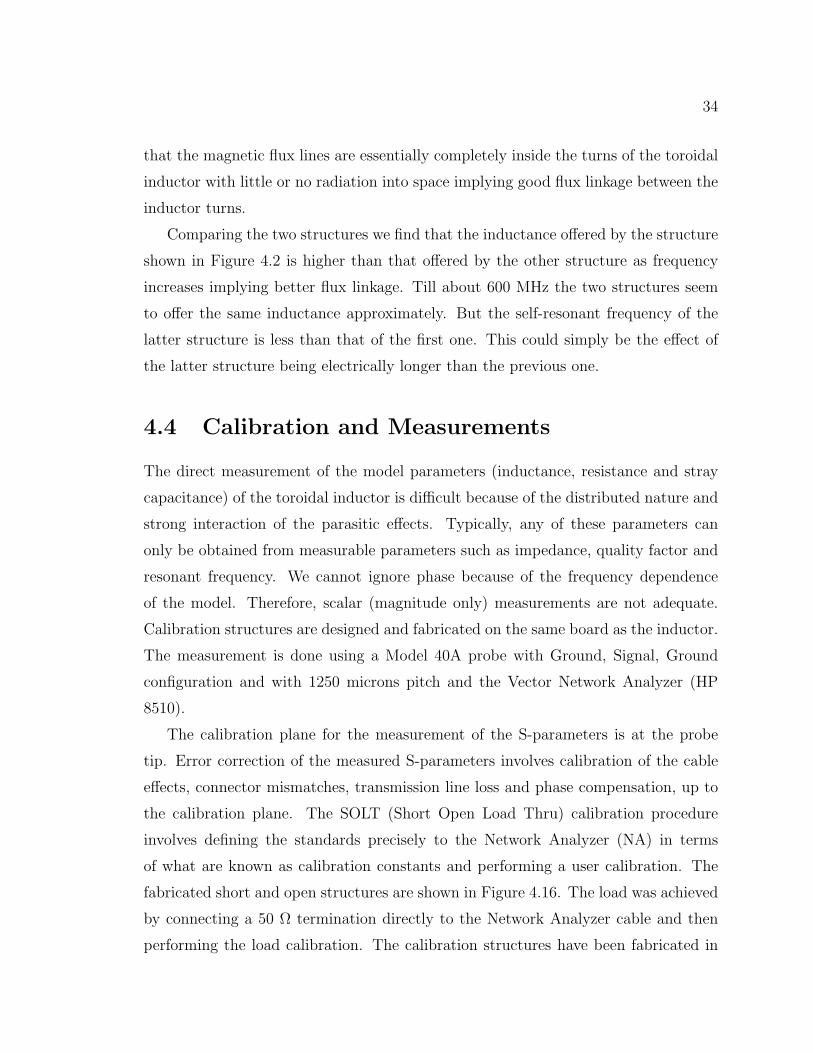
Figure 4.17: Top view of the toroidal structure with approximately equal anglesbetween each pair of top and bottom metal strips.
the way shown in order to take care of the capacitance at the feed lines so that the
effect it has on the measurement of the inductor is reduced.
The top and bottom views of the two structures fabricated are shown in Figures
4.17, 4.18, 4.19 and 4.20. The feed lines were designed to be 50Ω anywhere along the
lines. This was done using Sonnet.
The comparison between the measured and simulated results for the first structure
is shown below.
Looking at the smith chart in Figure 4.21 we see that the structure is inductive
till around 700 MHz. The inductance achieved is from 84 nH at 100 MHz to 0.2 µH
at resonance. The inductance achieved from the simulation in HFSS is from 83 nH at
100 MHz to 0.32 µH at resonance. The self-resonant frequency for the measurement
is around 450 MHz. The inductance values obtained from the measurement and the
simulation are quite comparable in Figure 4.22. The Q factor for the measurement is
around 170 which is far beyond what is obtained from the simulation as can be seen
in Figure 4.23.
The comparison between the measured and simulated results for the second struc-

37
Figure 4.18: Bottom view of the toroidal structure with approximately equal anglesbetween each pair of top and bottom metal strips.
Figure 4.19: Top view of the second toroidal structure.

38
Figure 4.20: Bottom view of the second toroidal structure.
ture is shown below.
Looking at the smith chart in Figure 4.24 we see that the structure is inductive till
around 500 MHz. The inductance achieved is from 93 nH at 100 MHz to 0.39 µH at
resonance. The inductance achieved from the simulation in HFSS is from 80.4 nH at
100 MHz to 0.32 µH at resonance. The self-resonant frequency for the measurement
is around 450 MHz. The inductance values obtained from the measurement and
the simulation are quite comparable as seen in Figure 4.25. The Q factor for the
measurement is around 150 which is far beyond what is obtained from the simulation
as can be seen in Figure 4.26.
The working of the inductor was verified in many ways, for example by introducing
a break in the metal strip. It was also verified using varying sizes of airbox around
each of the three variations of the toroidal inductor. Different values of width of metal
strip, different substrates (different values of dielectric constant), different metals for
the metal strip, different number of turns keeping the mean radius of the toroid
constant were some of the other techniques used.

39
0.2 0.5 1 2
j0.2
−j0.2
0
j0.5
−j0.5
0
j1
−j1
0
j2
−j2
0
simulated
measured
Figure 4.21: Smith Chart showing measured and simulated S11 for the first structure.

40
100 200 300 400 500 600 700 800 900 1000−300
−200
−100
0
100
200
300
400
Indu
ctan
ce(n
H)
frequency (MHz)
Simulated
Measured
Figure 4.22: Comparison of the measured and simulated inductance values for thefirst toroidal inductor structure.
100 200 300 400 500 600 700 800 900 1000−20
0
20
40
60
80
100
120
140
160
180
Q fa
ctor
frequency (MHz)
measured
simulated
Figure 4.23: Comparison of the measured and simulated quality factor values for thefirst toroidal inductor structure.

41
0.2 0.5 1 2
j0.2
−j0.2
0
j0.5
−j0.5
0
j1
−j1
0
j2
−j2
0
measured
simulated
Figure 4.24: Smith Chart showing measured and simulated S11 for the second struc-ture.

42
100 200 300 400 500 600 700 800 900 1000−300
−200
−100
0
100
200
300
400
Indu
ctan
ce (
nH)
frequency (MHz)
measured
simulated
Figure 4.25: Comparison of the measured and simulated inductance values for thethird toroidal inductor structure.
100 200 300 400 500 600 700 800 900 1000−20
0
20
40
60
80
100
120
140
160
Q fa
ctor
frequency (MHz)
measured
simulated
Figure 4.26: Comparison of the measured and simulated quality factor values for thethird toroidal inductor structure.

43
Chapter 5
Conclusions
5.1 Conclusions
The toroidal inductor has been presented as a viable candidate for use in RF and
microwave circuits on-chip or in-package. The structure has been simulated and
measured in a frequency range of 100MHz to 1GHz. Two variations of the toroidal
inductor have been simulated using Agilent’s High Frequency Structure Simulator
(HFSS) to study the effect of the placement of the top and bottom metal strips on
the flux linkage and hence, the inductance and quality factor of the inductor.
In the first structure, each pair of top and bottom metal strips are placed at
unequal angles with respect to each other. In the second structure, the top and
bottom metal strips are placed uniformly around the circumference. A radiation
boundary condition was applied to the airbox surrounding the toroid.
The simulation in HFSS yields a peak Q of 40 and a low frequency inductance
of 0.8nH compared to a measured low frequency inductance of 0.9nH. The mea-
sured peak Q is very large, greater than 40, and the traditional reflection coefficient
procedure cannot be used to determine a reliable value.
Both structures exhibit high inductance and high quality factor. The inductances
of the two structures have been found to be comparable except at resonance where the
inductance of the second structure becomes almost twice that of the first structure.
The self-resonant frequency of the first structure (900MHz) is better than that of the

44
second structure (800MHz). The quality factor of the second structure is observed to
be slightly lower than the first one. This could be simply because the second structure
is electrically longer than the first one.
Three toroidal inductor structures have been fabricated and measured using the
HP Vector Network Analyzer. The measurements indicate the self-resonant frequency
for these structures to be around 400MHz.

45
Bibliography
[1] Simon Ramo, John R. Whinnery, Theodore Van Duzer, Fields and Waves in
Communication Electronics, Wiley Publications, 1984.
[2] John D. Kraus, Electromagnetics, Mcgraw-Hill Publications, 1973.
[3] Reinhold Ludwig, Pavel Bretchko, RF Circuit Design Theory and Applications,
Prentice-Hall Publications, 2000.
[4] Chris Bowick, RF Circuit Design, Newnes Publications, 2001.
[5] HP High-Frequency Structure Simulator User’s Reference.
[6] Yeun-Ho Joung, Sebastien Nuttinck, Sang-Woong Yoon, Mark G. Allen, Joy
Laskar, “Integrated Inductors in the Chip-to-Board Interconnect Layer Fabri-
cated Using Solderless Electroplating Bonding,” 2002 IEEE MTT-S Int. Mi-
crowave Symp. Dig., 2002.
[7] Yong-Jun Kim, Mark G. Allen, “Integrated Solenoid-Type Inductors for High
Frequency Applications and Their Characteristics,” 1998 IEEE Electronic
Components and Technology Conf., Jun 1998.
[8] Krishna Naishadham, “Experimental Equivalent-Circuit Modeling of SMD In-
ductors for Printed Circuit Applications,”IEEE Trans. Electromagn. Compat.,
vol.43, Nov 2001, pp. 557–565.
[9] H.J.Ryu, S.D.Kim, J.J.Lee, J.Kim, S.H.Han, H.J.Kim, Chong H.Ahn, “2D
and 3D Simulation of Toroidal Type Thin Film Inductors,” MMM-Intermag
Conference, Jan 1998.

46
[10] Martin O’Hara, “Modeling Non-Ideal Inductors in SPICE,” Newport Compo-
nents, U.K. Nov 1993.
[11] Seogoo Lee, Jongseong Choi, Gary S.May, Ilgu Yun, “Modeling and Analysis
of 3-D Solenoid Embedded Inductors,” IEEE Trans. Electron. Packag. Manu-
facturing, vol.25, Jan 2002, pp. 34–41.
[12] William B. Kuhn, Aaron W. Orsborn, Matthew C. Peterson, Shobak R.
Kythakyapuzha, Aziza I. Hussein, Jun Zhang, Jianming Li, Eric A. Shumaker
and Nandakumar C. Nair, “Spiral Inductor Performance in Deep-Submicron
Bulk-CMOS with Copper Interconnects,” 2002 IEEE Radio Frequency Inte-
grated Circuits Symposium, Aug 2002, pp. 385–388.
[13] Randall W. Rhea, “A Multimode High-Frequency Inductor Model,” Applied
Microwave and Wireless, Dec 1997.
[14] Bahl, I. J., “High current handing capacity multilayer inductors for RF and
microwave circuits”,’ Int. J. RF and Microwave Computer-Aided Engineering,
Vol. 10, No. 2, March 2000, pp. 139–146.
[15] Volant, R., Malinowski, J., Subbanna, S. and Begle, E., “Fabrication of high
frequency passives on BiCMOS silicon substrates”,’ 2000 IEEE MTT-S Int.
Microwave Symp. Dig., June 2000, pp. 209–212.
[16] Kuhn, W. B., “Approximate analytical modeling of currrent crowding effects in
multi-turn spiral inductors,” 2000 IEEE MTT-S Int. Microwave Symp. Dig.,
June 2000, pp. 405–408.
[17] Pun, A. L. L., Tau, J., Clement, J. R. and Su, D. K., “Substrate noise coupling
through planar spiral inductor,” IEEE J. of Solid-State Circuits, Vol. 33, June
1998, pp. 877–884.
[18] Kim, C. S., Park, M., Kim, C.-H., Park, M.-Y., Kim S.-D., Youn, Y.-S., Park,
J.-W., Han, S.-H., Yu, H. K. and Cho, H., “Design guide of coupling between

47
inductors and its effect on reverse isolation of a CMOS LNA,” 2000 IEEE
MTT-S Int. Microwave Symp. Dig., June 2000, pp. 225–228.