delft university of technology transmission electron
TRANSCRIPT

Delft University of Technology
Transmission electron imaging in the Delft multibeam scanning electron microscope 1
Ren, Yan; Kruit, Pieter
DOI10.1116/1.4966216Publication date2016Document VersionFinal published versionPublished inJournal of Vacuum Science and Technology B: Nanotechnology and Microelectronics
Citation (APA)Ren, Y., & Kruit, P. (2016). Transmission electron imaging in the Delft multibeam scanning electronmicroscope 1. Journal of Vacuum Science and Technology B: Nanotechnology and Microelectronics, 34(6),[06KF02]. https://doi.org/10.1116/1.4966216
Important noteTo cite this publication, please use the final published version (if applicable).Please check the document version above.
CopyrightOther than for strictly personal use, it is not permitted to download, forward or distribute the text or part of it, without the consentof the author(s) and/or copyright holder(s), unless the work is under an open content license such as Creative Commons.
Takedown policyPlease contact us and provide details if you believe this document breaches copyrights.We will remove access to the work immediately and investigate your claim.
This work is downloaded from Delft University of Technology.For technical reasons the number of authors shown on this cover page is limited to a maximum of 10.

Transmission electron imaging in the Delft multibeam scanning electron microscope 1Yan Ren and Pieter Kruit
Citation: Journal of Vacuum Science & Technology B, Nanotechnology and Microelectronics: Materials,Processing, Measurement, and Phenomena 34, 06KF02 (2016); doi: 10.1116/1.4966216View online: http://dx.doi.org/10.1116/1.4966216View Table of Contents: http://avs.scitation.org/toc/jvb/34/6Published by the American Vacuum Society
Articles you may be interested in PMMA removal selectivity to polystyrene using dry etch approachJournal of Vacuum Science & Technology B, Nanotechnology and Microelectronics: Materials, Processing,Measurement, and Phenomena 34, 061802061802 (2016); 10.1116/1.4964881
Embedded silicon carbide “replicas” patterned by rapid thermal processing of DNA origami on siliconJournal of Vacuum Science & Technology B, Nanotechnology and Microelectronics: Materials, Processing,Measurement, and Phenomena 34, 060602060602 (2016); 10.1116/1.4965726
Prediction of surface topography due to finite pixel spacing in FIB milling of rectangular boxes and trenchesJournal of Vacuum Science & Technology B, Nanotechnology and Microelectronics: Materials, Processing,Measurement, and Phenomena 34, 061803061803 (2016); 10.1116/1.4967249
Electron beam lithography patterned hydrogen silsesquioxane resist as a mandrel for self-aligned doublepatterning applicationJournal of Vacuum Science & Technology B, Nanotechnology and Microelectronics: Materials, Processing,Measurement, and Phenomena 34, 061601061601 (2016); 10.1116/1.4963194

Transmission electron imaging in the Delft multibeam scanning electronmicroscope 1
Yan Rena) and Pieter KruitDepartment of Imaging Physics, Delft University of Technology, Lorentzweg 1, 2628 CJ Delft,The Netherlands
(Received 24 June 2016; accepted 14 October 2016; published 27 October 2016)
Our group is developing a multibeam scanning electron microscope (SEM) with 196 beams in
order to increase the throughput of SEM. Three imaging systems using, respectively, transmission
electron detection, secondary electron detection, and backscatter electron detection are designed in
order to make it as versatile as a single beam SEM. This paper focuses on the realization of the
transmission electron imaging system, which is motivated by biologists’ interest in the particular
contrast this can give. A thin sample is placed on fluorescent material which converts the
transmitted electrons to photons. Then, the 196 photon beams are focused with a large
magnification onto a camera via a high quality optical microscope integrated inside the vacuum
chamber. Intensities of the transmission beams are retrieved from the camera images and
constructed to form each beam’s image using an off line image processing program. Experimental
results prove the working principle of transmission electron imaging and show that details of
10–20 nm in images of biological specimen are visible. Problems encountered in the results are
discussed and plans for future improvements are suggested. VC 2016 American Vacuum Society.
[http://dx.doi.org/10.1116/1.4966216]
I. INTRODUCTION
Increasing the imaging throughput of scanning electron
microscopy (SEM) could be of great benefit for some applica-
tions, especially in biology. For example, making an image of
a complete zebra fish sagittal section at 1.6 nm pixel resolution
over an area of 1.5� 0.6 mm took four and half days.1
Acquiring a 3D image of a 400� 400� 1000 lm mouse corti-
cal volume, with the typical 4 nm resolution, is estimated to
take about 400 days, depending on the detection method
applied.2 It will surely help a lot if this imaging acquisition
time of 400 days is reduced to one or two days while still keep-
ing the imaging quality.
Multibeam technology is the only option to achieve this.
Several groups are doing these, e.g., Mohammadi-Gheidari
and Kruit,3 D. Zeidler and G. Dellemann,4 and Enyama
et al.5 Some published their experimental results, e.g.,
Mohammadi-Gheidari et al.,6 and Eberle et al.7 Zeiss also
released a commercial multibeam SEM (MBSEM) which
has 61 or 91 beams, with secondary electron (SE) detection.
Although SE imaging is popularly used in SEM, it is not
favored by biologists who want to get component informa-
tion from biological specimens. Backscatter electron (BSE)
imaging is more attractive to them because it mainly pro-
vides component information. SE imaging primarily pro-
vides topography information and very weakly reflects the
component information by so-called SE2s which are gener-
ated by BSE in the interaction volume,8,9 as shown in Fig. 1.
However, BSE imaging encounters problem when biolog-
ical tissues are sliced very thin. For good 3D structure recon-
struction, the slice needs to be about 30–40 nm thin.2 The
BSE generation is low in such thin slices, as it is linearly
proportional to the thickness of the tissue,8 as in
gðtÞ ¼ cðEÞNZ2qt; (1)
where g is the BSE generation coefficient, c is a constant for
one incident beam energy, N is the number of electrons per
unit volume, Z is the atomic number, q is the atomic density,
and t is the thickness of the tissue. BSE imaging needs a
long dwell time to obtain a decent image with such thin sam-
ples. Our imaging experience tells us that the dwell time
needs 10 ls for landing energy 5 keV using the concentric
backscatter detector in FEI Verios SEM when the tissue is
not heavily stained.
Transmission electron (TE) imaging offers another possi-
bility to produce good contrast imaging, because the trans-
mission signal, similar to the BSE signal, also carries the
composition and mass density information. For very thin tis-
sues, the TE generation coefficient can be estimated as
c ¼ 1� g; (2)
where c is the TE generation coefficient. When the sample is
very thin, c usually is much larger than g except when the
primary beam’s landing energy is so low that most primary
electrons are absorbed in the sample. For 10 keV landing
energy and a 50 nm biological tissue slice, c is even
>99%.10 So, it is easier to detect TE than to detect BSE for
thin tissue. This does not mean, however, that the TE signal
provides better imaging contrast or signal to noise ratio. This
is as complicated as comparing bright field imaging to dark
field imaging, and is beyond the scope of this paper.
Some researchers have already shown good quality TE
imaging results using biological specimens.10,11 Kuipers
et al. even proved that TE imaging quality was as good as,
or even better than BSE imaging quality in their research.12
Besides, since the invention of the transmission electron
microscope (TEM), biologists have used mainly bright field
transmission imaging for their low-to-medium resolutiona)Electronic mail: [email protected]
06KF02-1 J. Vac. Sci. Technol. B 34(6), Nov/Dec 2016 2166-2746/2016/34(6)/06KF02/10/$30.00 VC 2016 American Vacuum Society 06KF02-1
images. Such results have motivated us to develop a TE
imaging system in our MBSEM.
In this article, the optical system in our MBSEM (the
Delft MBSEM1) is briefly explained; the design principle of
TE imaging system in the Delft MBSEM1 is discussed in
detail and our first, low throughput experimental results
using off line image processing program are presented.
Problems encountered in the experiments are discussed, and
plans for future improvements are suggested. It is possible to
apply the technology used for the TE imaging in the Delft
MBSEM to other types of MBSEMs.
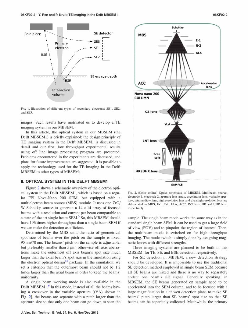
II. OPTICAL SYSTEM IN THE DELFT MBSEM1
Figure 2 shows a schematic overview of the electron opti-
cal system in the Delft MBSEM1, which is based on a regu-
lar FEI Nova-Nano 200 SEM, but equipped with a
multielectron beam source (MBS) module. It uses one ZrO/
W Schottky source to generate a 14� 14 array of focused
beams with a resolution and current per beam comparable to
a state of the art single beam SEM.3 So, this MBSEM should
have 196 times higher throughput than a single beam SEM if
we can make the detection as efficient.
Determined by the MBS unit, the ratio of geometrical
spot size of beams over the pitch on the sample is fixed,
95 nm/70 lm. The beams’ pitch on the sample is adjustable,
but preferably smaller than 5 lm, otherwise off axis aberra-
tions make the outermost off axis beam’s spot size much
larger than the axial beam’s spot size in the simulation using
the electron optical design13 package. In the simulation, we
set a criterion that the outermost beam should not be 1.2
times larger than the axial beam in order to keep the beams’
uniformity.
A single beam working mode is also available in the
Delft MBSEM1.6 In this mode, instead of all the beams hav-
ing a crossover in the variable aperture [(VA) shown in
Fig. 2], the beams are separate with a pitch larger than the
aperture size so that only one beam can go down to scan the
sample. The single beam mode works the same way as in the
standard single beam SEM. It can be used to get a large field
of view (FOV) and to pinpoint the region of interest. Then,
the multibeam mode is switched on for high throughput
imaging. The mode switch is simply done by assigning mag-
netic lenses with different strengths.
Three imaging systems are planned to be built in this
MBSEM: for TE, SE, and BSE detection, respectively.
For SE detection in MBSEM, a new detection strategy
should be developed. It is impossible to use the traditional
SE detection method employed in single beam SEM because
all SE beams are mixed and there is no way to separately
collect one beam’s SE signal. Generally speaking, in
MBSEM, the SE beams generated on sample need to be
accelerated into the SEM column, and to be focused with a
large magnification in a chosen detection plane to make SE
beams’ pitch larger than SE beams’ spot size so that SE
beams can be separately collected. Meanwhile, the primary
FIG. 2. (Color online) Optics schematic of MBSEM. Multibeam source,
electrode 1, electrode 2, aperture lens array, accelerator lens, variable aper-
ture, intermediate lens, high resolution lens and ultrahigh resolution lens are
abbreviated as MBS, E-1, E-2, ALA, ACC, INT lens, HR and UHR lens,
respectively.
FIG. 1. Illustration of different types of secondary electrons: SE1, SE2,
and SE3.
06KF02-2 Y. Ren and P. Kruit: TE imaging in the Delft MBSEM1 06KF02-2
J. Vac. Sci. Technol. B, Vol. 34, No. 6, Nov/Dec 2016

beams’ focusing will be modified but should not be disturbed
by the SE beams’ focusing and detection. In the Delft
MBSEM1, it is preferable to place the SE detector in a plane
(such as the VA plane) where the primary beams have a
common crossover in order to make the SE detection bring
as little disturbance as possible to the primary beams and to
keep the whole system compact. An electrostatic lens is
introduced to generate proper energy difference between the
primary beams and the SE beams, the difference which
makes it possible to use the same lenses to focus the primary
beams on the sample and to focus the SE beams in the detec-
tion plane. Some mechanical modification has to be done to
achieve the SE detection. The methods used in the Delft
MBSEM1 will be reported in a separate paper.
The BSE detection in MBSEM is more difficult than the
SE detection. In the conventional definition, BSE has an
energy range from 50 eV to the primary beam’s energy with
a full opening angle (from 0� to 90�). Such distribution
makes it very hard to separate one beam’s BSE signal from
its neighbors’. We are struggling to find a good solution and
as far as we know, no BSE detection system has yet been
successfully developed for MBSEM.
TE imaging does not need any modification to the pri-
mary beams’ focusing setup. This advantage makes it possi-
ble to apply the TE imaging system to every MBSEM. This
paper focuses on the realization of TE imaging in the Delft
MBSEM1.
III. TE IMAGING SYSTEM DESIGN IN DELFTMBSEM1
The first challenge of the TE detection is to separately col-
lect the TE signals because they have the same small pitch as
the primary beams have on the sample, smaller than 5 lm,
even smaller than 1 lm for 1.2 nm imaging resolution.3
There are at least two ways to do this. The first way is to
introduce an additional electron optical system to focus the
TE beams with a large magnification onto a detector where
the TE beams will be focused with a small spot size and
large pitch (at least larger than the largest spot size of
focused TE beams). TEM uses this strategy.14 In TEM, there
is no problem getting good focusing with large magnification
and one is free to choose between the bright field mode and
the dark field mode for different contrast. However, the dis-
advantage of utilizing this strategy in the MBSEM is that
new electron optical lenses need to be added. First, the sam-
ple chamber has a finite volume so that it is not easy to insert
new electron optical parts, including all the lenses, cables,
and connections. Second, the magnetic immersion objective
lens which is used to get the best resolution for the primary
beams focusing would interfere with the new add-on lenses.
Such an objective lens usually has strong excitation and a
very long tail.15 A little change of objective lens excitation
may spoil the add-on electron optical system. The combina-
tion of these two issues makes it difficult to implement this
strategy in this MBSEM.
The other way circumvents the interference issue by con-
verting electrons to photons using fluorescent material.
When the TE beam’s pitch is larger than the photon genera-
tion volume size in the fluorescent material, the 196 separate
TE beams create 196 separate light sources. An optical
microscope is then used to image these light sources with a
large magnification onto a camera. This optical microscope
should be capable of working inside the vacuum, providing
better resolution than the beams’ pitch, providing a large
numerical aperture (NA) for a high collection efficiency, and
having good alignment with the SEM column. The difficulty
of this strategy is in adding such an optical microscope into
the SEM’s sample chamber. In our group, we had just devel-
oped such a platform for correlative light-electron micros-
copy, the “SECOM platform,”16 further commercialized by
Delmic, a spinoff company in the Netherlands. This platform
places the optical microscope inside the vacuum chamber,
shown in Fig. 3, and uses the vacuum glass window to transit
light between the air environment and the vacuum chamber.
It is designed for biological research. Here, we employ this
SECOM platform for TE imaging, as schematically shown
in Fig. 4.
This strategy has limitations. One limitation is the resolu-
tion of optical microscopes. Due to the diffraction limitation,
submicrometer resolution is difficult to achieve unless we
use liquid immersion lenses. This strategy probably will fail
when the primary beams’ pitch on the sample is smaller than
1 lm. In terms of resolution, a larger than 1 lm pitch on the
sample leads to no better than 3 nm optical imaging resolu-
tion of the Delft MBSEM1 because the ratio of geometrical
spot size of beams over pitch on the sample is fixed, 95 nm/
70 lm.
Another limitation is that the sample should be closely
placed on the fluorescent material. When there is a 1 mm gap
between the sample and the fluorescent material, if we
assume that TE beams have a similar opening angle as the
FIG. 3. (Color) View of integrated optical microscope in SEM chamber.
06KF02-3 Y. Ren and P. Kruit: TE imaging in the Delft MBSEM1 06KF02-3
JVST B - Nanotechnology and Microelectronics: Materials, Processing, Measurement, and Phenomena

primary beams, typically 10 mrad, a TE beam grows to be a
spot of 20 lm, much larger than the pitch. Neighboring TE
beams will mix together in the fluorescent material. So, it is
recommended that thin tissue will be directly placed on the
fluorescence material to restrain TE beams’ spread. The con-
sequence of this placement is that there is no bright field
mode and dark field mode anymore in this TE imaging sys-
tem because all of the transmitted electrons from a primary
beam have been collected. Additionally, it will be difficult to
remove thin tissues from the fluorescent material without
damage.
After comparing these two options, the latter was chosen,
that of using the SECOM platform.
The remaining challenge is to detect the intensities of the
TE beams. We want to read each beam’s TE signal out in
each scan step for live imaging. One possible way is to use a
detector array, one detector for one beam. This concept is
employed in the Zeiss’ MBSEM for SE detection and is
quite a straightforward method. In the scanning, one beam’s
signal should always fall into its own detector. Considering
that the scanning FOV is usually equal to or a bit larger than
the beam’s pitch, it is necessary to have descan system
which is synchronized with the primary beam deflectors to
compensate the TE signal shift on the detector.
It is also possible to use a CCD or CMOS camera and fast
image processing technology to detect the intensities. A
camera image of the 196 light sources (or the 196 TE beams)
is generated in each scan step, an example of which is shown
in Fig. 5. These 196 beams’ intensities can be retrieved from
such an image and assigned to corresponding beams using
an image processing program. For live imaging, these two
steps need to done in one scan dwell time.
The advantage of the first option is that each subdetector
is similar to a normal detector; so, it is easy to process
detected signals. The disadvantages are that we need to add
a descan system, and that thousands of electronic cables and
controls need to be used for detector array. Plenty of modifi-
cations have to be made to the SEM column for this option
to be viable.
The advantage of the second option is that it is easy to
start because all parts are commercially available for the
concept proof test, and the whole detection unit is compact.
A disadvantage is that it is very demanding for the camera
and the image processing program. If 100 ns dwell time is
used—the dwell time which is normally used in single beam
SEM for fast scanning—the camera needs to have 10 �106
frames per second (FPS) rate and very good sensitivity. If
one TE spot needs 10� 10 camera pixels to record, then
there should be more than 19 600 pixels in one camera
image. The first problem is that such a camera is both rare
and expensive. The second problem is that of transferring
and processing 196 GByte data in one second when each
pixel has 8 bit depth.
It is hard to tell which one is better, or easier for the TE
detection in the Delft MBSEM1. We have chosen an easy
start: the combination of a camera and fast image processing
technology to prove the working principle of the TE detec-
tion system. It is not necessary to use a 10M FPS camera in
the beginning stage because it is expensive and complicated
to transfer data and process the images so rapidly. We divide
the TE imaging system development into three steps. In the
first step, off-line image processing with the low throughput
imaging method is employed to prove this imaging concept.
The camera “Prosilica GE680” from Allied Vision Tech is
utilized. It has 7.4 lm pixel size and 205 frames per second
FIG. 4. (Color) Combination of Delft MBSEM1 and SECOM platform.
FIG. 5. Image of 196 beams with pitch 4 lm onto an YAG (Y3Al5O12)
screen and recorded by a camera.
06KF02-4 Y. Ren and P. Kruit: TE imaging in the Delft MBSEM1 06KF02-4
J. Vac. Sci. Technol. B, Vol. 34, No. 6, Nov/Dec 2016

at a resolution of 640� 480. A Nikon 40� objective lens is
used in the optical microscope to have a 40 times magnifica-
tion. A camera image with 196 TE beams information is
saved into a computer in each scan step during a scan period.
Then, the off-line image processing program is used to cal-
culate each beam’s intensity and position in each scan step
and then use all the intensities in a scan period to construct
its TE image and the whole TE image map. The experimen-
tal results shown in Sec. IV of this paper were obtained using
this off-line method.
In the second step, a slow real time imaging program based
on field programmable gate arrays (FPGA) technology is
developed.17 A FPGA stands between the camera and the
computer. The camera continuously sends images via a camera
link to the FPGA where an image processing algorithm is writ-
ten to calculate each beam’s intensity in each scan step. The
algorithm builds a beams’ mask based on one TE beam’s
image before the real time imaging starts. In the real time
imaging, the mask shifts, synchronized with the beams’ scan
step, and is used to calculate the beams’ intensities quickly in
each scan step and to assign intensities to the 196 beams.
Then, the FPGA sends these intensities’ information to the
computer where a Labview program is used to construct TE
images. The goal of this step is to achieve a slow real time
imaging at a camera rate of several thousand frames per sec-
ond. In the final step, the fast real time imaging will be realized
by utilizing a very fast camera (such as the 10M FPS camera).
To sum up, the TE imaging system of the Delft MBSEM1
adopts a SECOM platform with fluorescent material to con-
vert electrons to photons, a camera, and fast image process-
ing technology. Section IV presents experimental results
from off-line processing.
IV. EXPERIMENTAL RESULTS
In the experiment, yttrium aluminum garnet [(YAG),
Y3Al5O12] is chosen to convert electrons to photons, because
it has a very high conversion efficiency (about 21 photons/
keV/electron for low beam energy) and short decay time (70
ns, which is short enough for our current experiments), in
addition to being commercially available in different sizes
and thicknesses. Our YAG with a thickness of 20 lm and
also the source of the YAG data are supplied by the company
“Crytur.”
A. Sample information
In the experiments, two types of samples are used. One is
a calibration sample, shown in Fig. 6. These patterns are
made by depositing tungsten on top of YAG. The line pat-
terns have 1 lm pitch and 0.5 lm line width, and the hole
patterns have 0.6 lm pitch and 0.4 lm diameter. The reason
to use this calibration sample is that in the Delft MBSEM1,
though using the original FEI column, the focusing condition
and the lens combinations are different than in the original
FEI setup. Thus, scan FOV and magnification shown in FEI
user interface are not correct. This sample can be used to cal-
ibrate scan FOV.
The other type is rat pancreas tissue provided by UMCG
Groningen (Giepmans group) in the Netherlands. The
heavily stained sample has a thickness of 100 nm. These
samples are directly placed on top of a YAG disk which has
50 nm aluminum coating for conduction and for reflecting all
photons to the optical microscope. Although in principle TE
imaging is capable of getting good contrast images with little
or no stained sample, here the heavily stained sample is used
in the experiments. The reason is that the detection chain in
the TE imaging system in the Delft MBSEM1 is still in its
first development phase and many factors have influence on
the TE imaging detection efficiency and the imaging
FIG. 6. (Color online) Calibration sample: the color part is electron transpar-
ent area and the white is tungsten. Lines: 0.5 lm wide, 1 lm pitch; holes:
0.4 lm diameter, 0.6 lm pitch.
FIG. 7. (Color online) Overview of the samples using single beam mode in
order to select region of interest quickly. (a) The calibration sample; (b) the
biological sample.
06KF02-5 Y. Ren and P. Kruit: TE imaging in the Delft MBSEM1 06KF02-5
JVST B - Nanotechnology and Microelectronics: Materials, Processing, Measurement, and Phenomena

contrast, for example, the choices of camera and fluorescent
material, and even the way we prepare the tissues on YAG.
Now, we are struggling to find the proper way to place thin
tissues on the YAG. So, it is better to start from the sample
which is heavily stained and can easily give good contrast
images in order to prove the working principle.
B. Imaging results in Delft MBSEM1
All the experiments in this section are done using a land-
ing energy of 15 keV in the Delft MBSEM1.
1. Single beam mode imaging
In the operation, it is preferable to use single beam mode
to have an overview of the sample and then to select the
region of interest (Fig. 7).
2. Multibeam mode imaging
The 196 beams are labeled by using four quadrants,
shown in Fig. 8. Beams from different locations in the E-
beam grid give similar performance using the calibration
sample, shown in Fig. 9. These images are used to calibrate
the scan FOV and scan magnification.
Figures 10 and 11 show TE images of the rat pancreas tis-
sue sample. The beams, regardless of whether from the cen-
ter or from the edge of the E-beam grid, give quite an even
imaging quality.
The image map is constructed by stitching the 196 TE
images. In this process, beams’ scan direction needs to be par-
allel with one side of E-beam grid. In principle, the scan FOV
can be equal to the pitch of the E-beam grid on the sample so
that no stitching program is needed afterward, which is our
goal. Then, the beam scan direction and scan FOV need to be
accurately set. This can be done after several attempts on a cer-
tain working condition and will easily be done when real time
imaging is available. Currently, however, it takes too much
time because off-line image processing is used. In this stage, it
is not necessary because we just intend to prove the working
concept, not to deliver the perfect image map which is the goal
of our imaging system in the future. Now we align the scan
direction with the E-beam grid coarsely and set scan FOV to
10%–20% larger than the pitch of the E-beams on the sample,
and then construct an image map using a stitching software
called “TRAKEM2.”18 In this way, the beams’ images may show
slight rotation with respect to the beam array in the image map
because the scan direction is not accurately aligned with one
side of the E-beam grid on the sample. This is demonstrated in
FIG. 8. Beams are labeled by four quadrants in the grid.
FIG. 9. Different beam’s TE image using calibration sample. They are cap-
tured simultaneously and their FOV of images is 1.0 lm. Scale bars 200 nm.
FIG. 10. Different beams’ TE images using pancreas tissue captured simulta-
neously; they have FOV 4.0 lm with 20 nm pixel size. Scale bars 1 lm.
06KF02-6 Y. Ren and P. Kruit: TE imaging in the Delft MBSEM1 06KF02-6
J. Vac. Sci. Technol. B, Vol. 34, No. 6, Nov/Dec 2016

Figs. 12 and 13 which show image maps with 25 and 50 lm
FOV, acquired by using different E-beam grid pitches on the
sample. No stitching is applied in these two figures. This scan
direction misalignment shows more clearly in the image map
after stitching. In the stitching, the subimage overlap is set,
and the linear blending fusion method embedded in the
TrackEM2 is applied. The image map seems tilted at a small
angle, leaving some dark areas near the boundary of the image
map frame, as in Figs. 14 and 15, which show image maps of
biological tissue after stitching, with FOV 50 lm with
2600� 2500 pixels. Figure 14 has more misalignment between
beams’ scan direction and one side of the E-beam grid; so, its
image map has a larger dark area near the frame boundary.
V. DISCUSSION
A. Present imaging speed and image size
In this paper, these results are used to demonstrate the
principle of TE imaging. It now takes us about 20 min to
FIG. 11. Different beams’ TE images using pancreas tissue recaptured simul-
taneously; they have FOV 0.8 lm with 4 nm pixel size; details of 10–20 nm
are visible in these images. Scale bars 200 nm.
FIG. 12. TE image map of calibration sample formed by 14� 14 subimages
using Delft MBSEM1, without stitching, FOV 25 lm with 2800� 2800
pixels.
FIG. 13. TE image of calibration sample formed by 14� 14 subimages using
Delft MBSEM1, without stitching, FOV 50 lm with 2100� 2100 pixels.
FIG. 14. TE image map 1 of pancreas tissue formed by 14� 14 subimages
using our MBSEM, FOV 50 lm with 2600� 2500 pixels. Subimages are
stitched using the software TRAKEM2.
06KF02-7 Y. Ren and P. Kruit: TE imaging in the Delft MBSEM1 06KF02-7
JVST B - Nanotechnology and Microelectronics: Materials, Processing, Measurement, and Phenomena

finish one TE image map. The image maps with FOV 50 lm
have 2600� 2500 pixels. The pixel size in the image maps
is around 20 nm. Clearly, this is not yet high resolution and
high throughput imaging. The following paragraphs explain
briefly why we cannot achieve high resolution and high
throughput imaging yet in our MBSEM.
The GE680 camera is not very fast, just 240 FPS when
the camera delivers an image of 400� 400 pixels. When the
beams’ scan resolution is 200� 200, it takes this camera 3
min. The image processing program takes about 17 min to
analyze camera images and to construct TE images. These
make the imaging speed low in the TE imaging system in
the Delft MBSEM1, unsurprising considering that the off-
line processing mode is used.
In each scan step, the useful information that we really
want is the 196 beams’ intensities and positions. It is 588
Byte if each parameter takes 1 byte to record. However, in the
off-line processing mode, the camera sends an image with
400� 400 pixels with 8 bit depth to the computer. This is 160
kByte, 271 times more than what we need. If the beams’ scan
resolution is 200� 200, the camera will generate 6.4 GByte
data in one scan period although the useful information is just
23.5 Mbyte. Our current test program, based on LabVIEW, is
capable of handling no more than 8 GByte data in one scan
period. So, the scan resolution cannot be set to be 500� 500
if a camera image still has 400� 400 pixels. This limited scan
resolution makes large pixel size or scan step size in TE
images even larger than the primary beam’s spot size on the
sample. For example, when a beam’s scan FOV is 4 lm, each
scan step is 20 nm using 200� 200 scan resolution, while the
expected primary beam resolution is about 12 nm calculated
in the simulation. The camera and the test program limit the
size and imaging resolution in the image maps.
This low imaging throughput and small image size will
be improved in the planned TE imaging system
development. For example, in the second step, a faster cam-
era, the Optronis CL600� 2 CMOS, is used, which has 2000
FPS when each camera image has 512� 512 pixels.
Additionally, FPGA is used to process images much more
rapidly. It is able to send 5.4 Gbyte per second from the
CL600� 2 camera to the frame grabber with on board
FPGA (NI PCIe-1473R) via the FPGA camera link. The
FPGA processes the camera images to generate the 196
beams’ intensities and positions, and sends this useful infor-
mation to a computer where TE images are constructed.
Then, it will take about 20 s—instead of 20 min—to finish
the image maps we had now, 60 times faster. The imaging
throughput in the Delft MBSEM1 will then be higher than
that of a single beam SEM, but still lower than that of the
commercial MBSEM. However, it will allow a scan step
smaller than the expected size of the primary beams so that
the resolution can be measured and optimized. After the
third development step, the fast real time imaging will be
available and the Delft MBSEM1 should deliver the high
resolution and high throughput TE imaging.
Although such limitations exist in our current imaging
system, this test Labview program is already able to check
fine features of the samples by setting a small FOV (smaller
than the TE beams pitch on the sample). Figure 11 shows
four TE images with FOV 0.8 lm and examples of
400� 400 scan resolution while the pitch of E-beam grid on
the sample is 1.8 lm. The details of 10–20 nm size can be
seen in these images. It would be premature at this time to
state our MBSEM’s imaging resolution because biological
tissue itself and these images are not suitable for evaluating
imaging resolution. Although we tried to deposit gold par-
ticles (the mixture of 5 nm gold particles, 15 nm gold par-
ticles, and 50 nm gold particles) on a YAG disk to test
resolution, the gold particles clustered together and it was
not possible to test resolution at all. A special resolution test
sample is needed to test resolution in this TE imaging sys-
tem, for example, line or dots patterns with the size of a few
nanometers deposited on YAG using electron beam induced
deposition or similar microelectromechanical systems
technology.
B. Intensity differences in image map
There are quite clear intensity differences among neigh-
boring subimages in the image maps. The possible causes of
this nonuniformity are as follows:
(1) Different beams’ currents due to contamination in the
aperture lens array (ALA) which splits the original beam
into multiple beams. This would not be surprising after
five years of using the same aperture plate.
(2) Misalignment in the MBSEM column, resulting in dif-
ferent beams being differently aligned on the variable
aperture, thus selecting different currents.
(3) Some imperfection in the detection chain and the image
processing.
The first cause has already been proved by checking a
sample without any pattern, such as pure YAG. When all
FIG. 15. TE image map 2 of pancreas tissue formed by 14� 14 subimages
using our MBSEM, FOV 50 lm with 2600� 2500 pixels. Subimages are
stitched using the software TRAKEM2.
06KF02-8 Y. Ren and P. Kruit: TE imaging in the Delft MBSEM1 06KF02-8
J. Vac. Sci. Technol. B, Vol. 34, No. 6, Nov/Dec 2016

primary beams come down to that sample without using any
aperture in the column, quite a few beams’ profiles are not
round any more, but with irregular shapes. This tells us that
some apertures of the ALA in the MBS are contaminated.
This contamination needs to be verified by using a standard
SEM. However, in order to take the aperture array out, the
whole MBS needs to be disassembled. The MBSEM needs
to be shut down at least for one month. This verification was
subsequently postponed until the time that the emission tip
needs to be replaced.
The primary beams have a common crossover in the vari-
able aperture plane so that apertures here are used to choose
different currents. Because of the spherical aberration in the
accelerator (ACC) lens (in this paper, only the ACC lens is
used to form the common crossover and the C2 lens is off),
the off axis beams are shifted a bit away from the axis. After
the variable aperture, the central portion of the axial beam is
selected, but a different portion of the off axis beams is
selected. Once the electron optics is fixed, these selections
really depend on the position of the variable aperture. The
misalignment, together with contamination in the aperture
array, makes the current selection for off axis beams a bit
unpredictable.
The optical microscope may make the off axis beams lose
more photons than the axial beam. The uniformity of the
camera pixels’ output and the image processing program
may also introduce some intensity difference even when the
electron optical side is perfect. So, an intensity match pro-
gram is needed to eliminate or greatly reduce this nonuni-
form intensity inside the image map in the future.
C. Crosstalk influence
Figure 16 shows the line profiles in two E-beam grids. It
is obvious that there is a crosstalk among neighboring beams
even at 4 lm pitch. However, we cannot see the crosstalk
effect contribution in sub-beam images. So, in this paper, we
neglect the crosstalk influence, but we believe that when the
e-beam grid pitch becomes close to the size of one beam
inside the YAG, this influence will be problematic.
This crosstalk effect can be measured. For example, a sin-
gle beam SEM and the Delft MBSEM1 image the same area
in a sample using the same detection system. The single
beam SEM image has the real sample information. The
MBSEM image has the real sample information plus the
crosstalk influence. Each pixel’s intensity in the MBSEM
image minus the corresponding pixel’s intensity in single
beam SEM image reveals the crosstalk influence. The deteri-
oration of the imaging quality due to the crosstalk effect
should be analyzed based on specific application.
D. Subimage boundary in image map
Some subimages’ boundaries are apparent in the image
maps, as can be seen in Figs. 14 and 15, even after different
diffusion methods (such as linear blending, average, median,
max intensity, etc.) are tried in the TRAKEM2. This is a com-
mon but very tough challenge in the stitching. So far, it is
popular to use automatic stitching with the help of manual
FIG. 16. (Color online) Line profiles in E-beam grid with 4 lm pitch and 1.5
lm pitch. In (a), there are patterns on the YAG; in (b) there is no pattern on
the YAG.
06KF02-9 Y. Ren and P. Kruit: TE imaging in the Delft MBSEM1 06KF02-9
JVST B - Nanotechnology and Microelectronics: Materials, Processing, Measurement, and Phenomena

stitching in the construction of image maps. However, as
there are 196 subimages generated in this MBSEM in one
scan period, it is hardly possible to do manual stitching. A
good automatic stitching program is expected to take a long
calculation time. Meanwhile, we can make improvements by
aligning the scan direction well with the e-beam grid direc-
tion and matching the scan FOV well with e-beam grid
pitch.
VI. CONCLUSION AND OUTLOOK
This article provides one method to achieve TE imaging
in the Delft MBSEM1. In this image system, YAG is
adopted to convert the 196 TE beams to 196 photon beams;
an optical microscope with high NA and good alignment
with the electron optical axis is used inside the sample cham-
ber to focus the 196 photon beams on to a camera with large
magnification. An off line image processing program is used
to retrieve each beam’s transmission signal and construct
images. A calibration sample and biological tissues are
imaged to prove the working principle of this method.
Limited by the camera and the test Labview program, the
imaging throughput is low, approximately 20 min to finish
images of one scan period with low scan resolution
(200� 200). Our second step of TE imaging system devel-
opment is underway and should deliver relatively fast (a few
thousand scan steps per second) real time imaging with a
faster CMOS camera “Optronis CL600� 2” and a FPGA
based image processing program. Our ultimate goal is to
achieve rapid (100 ns scan dwell time) real time imaging
using a super-fast camera (at least with 10M FPS).
In the second and third development steps, the whole
detection chain also needs to be optimized, such as the
choices of the camera and the fluorescent material, the way
to prepare the sample in the TE imaging system in the Delft
MBSEM1, etc. The study of the imaging properties, includ-
ing the image contrast, the detection quantum efficiency, and
the optimum imaging throughput, needs to be carried on
when the real time imaging is available.
The imaging resolution of TE images from the Delft
MBSEM has not yet been measured because the proper reso-
lution test sample needs to be prepared, preferably having a
few nanometer scale patterns on a fluorescent material, but
the details of 10–20 nm in images of biological specimen are
visible in the TE images. The intensity difference in the
image maps is clearly shown in the image maps. In the
future, elements such as the aperture array, the electron
optics alignment, and image processing program need to be
checked for correction. The crosstalk among neighboring
beams in the E-beam grid is found in the experiments but is
not clearly shown in the TE images. When the pitch of E-
beam grid on the sample is close to the size of one beam in
the YAG, it will give problems. Its influence in TE images
should be analyzed in the future. A good stitching program
and/or good control of the beam scan direction and scan
FOV will be helpful in eliminating the subimages’ boundary
in the image map.
ACKNOWLEDGMENTS
The authors acknowledge Jacob Hoogenboom for advice
on biological imaging, Kees Hagen for discussions, Christiaan
Zonnevylle for help with the SECOM platform and discussion
on TE imaging system buildup, Ben Giepmans’ group for
biological tissue preparation, and Thomas Verduin, Paul
Keijzer, Wilco Zuidema, and Lennard Voortman for assistance
with the image processing program.
1F. G. Faas, M. C. Avramut, B. M. van den Berg, A. M. Mommaas, A. J.
Koster, and R. B. Ravelli, J. Cell Biol. 198, 457 (2012).2K. L. Briggman and D. D. Bock, Curr. Opin. Neurobiol. 22, 154 (2012).3A. Mohammadi-Gheidari and P. Kruit, Nucl. Instrum. Methods A 645, 60
(2011).4V. Marx, Nature 503, 147 (2013).5M. Enyama, M. Sakakibara, S. Tanimoto, and H. Ohta, J. Vac. Sci.
Technol., B 32, 051801 (2014).6A. Mohammadi-Gheidari, C. W. Hagen, and P. Kruit, J. Vac. Sci.
Technol., B 28, C6G5 (2010).7A. L. Eberle, S. Mikula, R. Schalek, J. Lichtman, M. L. K. Tate, and D.
Zeidler, J. Microsc. 259, 114 (2015).8L. Reimer, Scanning Electron Microscopy: Physics of Image Formationand Microanalysis (Springer, Verlag, Berlin, Heidelberg, 1998).
9J. Cazaux, J. Microsc. 214, 341 (2004).10A. Takaoka and T. Hasegawa, J. Electron Microsc. 55, 157 (2006).11P. G. Merli and V. Morandi, Microsc. Microanal. 11, 97 (2005).12J. Kuipers, P. de Boer, and B. N. G. Giepmans, Exp. Cell Res. 337, 202
(2015).13B. Lencova and J. Zlamal, Electron Optical Design program package
EOD3.069, 2006.14L. Reimer, Transmission Electron Microscopy: Physics of Image
Formation and Microanalysis (Springer, Verlag, Berlin, Heidelberg, 1997).15J. Orloff, Handbook of Charged Particle Optics (CRC, Boca Raton,
1997).16A. C. Zonnevylle, R. F. C. Van Tol, N. Liv, A. C. Narvaez, A. P. J.
Effting, P. Kruit, and J. P. Hoogenboom, J. Microsc. 252, 58 (2013).17S. Rahangdale, P. Keijzer, and P. Kruit, 2016 International Conference on
Systems, Signals and Image Processing (IWSSIP) (2016).18A. Cardona and S. Saalfeld, TRAKEM2 v. 1.0c, ImageJ, 2014.
06KF02-10 Y. Ren and P. Kruit: TE imaging in the Delft MBSEM1 06KF02-10
J. Vac. Sci. Technol. B, Vol. 34, No. 6, Nov/Dec 2016