transmission electron microscopy and diffraction - … · transmission electron microscopy ... 2)...
TRANSCRIPT
Aïcha Hessler-Wyser 1 CiMe
MSE637: introduction to TEM
Transmission Electron Microscopy and Diffraction
Dr Aïcha Hessler-Wyser, Dr Marco Cantoni, Dr Duncan Alexander
Centre Interdisciplinaire de Microscopie Electronique (CIME) Photovoltaics and Thin-Film Electronics Laboratory (PV-lab)

Aïcha Hessler-Wyser 2 CiMe
MSE637: introduction to TEM
Outline
a. Planning and ogranization b. A little about diffraction c. What can be done with a TEM? d. Why electrons? e. Electron-matter interaction

Aïcha Hessler-Wyser 3 CiMe
MSE637: introduction to TEM
a. Planning MSEͲ637 TEM�Ͳbasics1st 2nd 3rd
COͲ121 COͲ12108:15 7)�Diffraction�techniques 10)�examples
CBED,�Kikuchi,�HOLZ,�map Imaging�with�diffraction�09:00 DA contrast��DA
09:15 8)�HRTEM�ͲI 10)�examplesindexing�of�dif�Pat
10:00 COͲ121 MC DA10:15 1)�Intro HRTEMͲII 11)�Indexing�practicals
Basics�of�TEM,�eͲ�scattering11:00 AHW MC DA
11:15 2)�electron�optics 9)�Spec�prep 11)��Application�examplessources,�Lenses inͲsitu
12:00 MC DA AHW
COͲ121 COͲ121�/�mxc30/mxc03313:15 3)�diffraction�basics DEMO
crystallography,�Bragg�law14:00 DA OSIRIS�mxcͲ030
14.15 4)�electron�diffractionintensities�and�imaging CM12�mxcͲ033
15:00 DA15:15 5)�TEM�basic�imaging Spec�Prep�browser
contrast,��BF/DF (laptop�required)16:00 AHW
16:15 6)�TEM�image�and�diffSAED
17:00 AHW

Aïcha Hessler-Wyser 4 CiMe
MSE637: introduction to TEM
Slides available at http://cime.epfl.ch Please sign the presence sheet to get your credits Demo will be organised according to separated schedule, M. Cantoni will explain Exam: written, XX.YY.14, 3 pages report to hand in at the exam.
a. Administrative points: ED MS-636

Aïcha Hessler-Wyser 5 CiMe
MSE637: introduction to TEM
a. Training
TEM
– Theory MS637 mandatory – Practical training: to be arranged with CIME's staff
after application (forms available on http://cime.epfl.ch)

Aïcha Hessler-Wyser 6 CiMe
MSE637: introduction to TEM
b. Little history
1665 2007

Aïcha Hessler-Wyser 7 CiMe
MSE637: introduction to TEM
b. Little history: optics
Optical microscopy Antiquity: first etch of convex lenses
XII-XIIIth centuries: magnification power of convex lenses, magnifier, glasses
1590 Janssen, first composed microscope
1609 Galilei: occhiolino
1665 Hooke: first cell image
1801 Young: wave nature of light
1872 (~) Abbe: the resolution limit is linked to wave length of the used beam

Aïcha Hessler-Wyser 8 CiMe
MSE637: introduction to TEM
b. Little history: electrons?
Electron microscopy 1923 De Broglie: concept of wavelength associated to
particles, confirmation by Young's experiment 1927 Busch: focalisation low for magnetic fields
Davisson, Germer, Thomson: electron diffraction 1931 Ruska, Knoll: first images by electron microscopy

Aïcha Hessler-Wyser 9 CiMe
MSE637: introduction to TEM
b. Little history: electrons?
Electron microscopy 1923 De Broglie: concept of wavelength associated to
particles, confirmation by Young's experiment 1927 Busch: focalisation low for magnetic fields
Davisson, Germer, Thomson: electron diffraction 1931 Ruska, Knoll: first images by electron microscopy

Aïcha Hessler-Wyser 10 CiMe
MSE637: introduction to TEM
b. Little history: electrons?
1936 Scherzer: main electromagnetic lens aberrations cannot be avoided
1938 Von Ardenne: first microprobe scanning electron microscope
1939 Siemens: first industrial electron microscopes
1948 Gabor: holography invention
1951 Castaing: first X-ray micro-analyser
1960 XX: first MV microscope, competition for resolution
1965 Crewe: first scanning transmission electron microscope
1982 Binnig et Rohrer: scanning tunnelling microscope
1986 Ruska, Binnig et Rohrer: Prix Nobel Physics
1990 Rose: proposes the Cs corrector principle
1995 Haider: first realisation of the Cs corrector

Aïcha Hessler-Wyser 11 CiMe
MSE637: introduction to TEM
b. Little history: resolution?
Resolution evolution with time and new technologies
0.0001
0.001
0.01
0.1
1
1800 1840 1880 1920 1960 2000 2040
Res
olut
ion
(An
g.-1)
Year
Electron Microscope
Light Microscope
Corrected EM
Ross
Amici
Abbe
Ruska
Marton
Dietrich(200keV)
Haider(200keV)
H. Rose, 1994 TEAM project, 2002

Aïcha Hessler-Wyser 12 CiMe
MSE637: introduction to TEM
a detector (eye, photographic plate,
video camera...
an illumination section (lenses, apertures...)
a magnification section (lenses, apertures...)
a sample (+ a "goniometer")
A "light" source
c. What can be done with a TEM?

Aïcha Hessler-Wyser 13 CiMe
MSE637: introduction to TEM
c. What can be done with a TEM?

Aïcha Hessler-Wyser 14 CiMe
MSE637: introduction to TEM
c. What can be done with a TEM?
Different signals Different detectors
= Different informations!
1. Interaction of electrons with matter

Aïcha Hessler-Wyser 15 CiMe
MSE637: introduction to TEM
c. What can be done with a TEM?
Electron source
Lenses
Detectors
Pumping unit
2. Electron optics

Aïcha Hessler-Wyser 16 CiMe
MSE637: introduction to TEM
c. What can be done with a TEM?
Electron diffraction
3. Basics of diffraction
4. Diffraction 7. Diffraction
techniques

Aïcha Hessler-Wyser 17 CiMe
MSE637: introduction to TEM
c. What can be done with a TEM?
Conventional TEM BF, DF Basics of electron diffraction (SAED)
5. TEM principles 6. Diffraction
contrast

Aïcha Hessler-Wyser 18 CiMe
MSE637: introduction to TEM
c. What can be done with a TEM?
Phase contrast Atomic column imaging High resolution
8. HRTEM

Aïcha Hessler-Wyser 19 CiMe
MSE637: introduction to TEM
c. What can be done with a TEM?
3mm m
ax. 2.4
mm
.
3mm.
9. Sample preparation

Aïcha Hessler-Wyser 20 CiMe
MSE637: introduction to TEM
d. Why electrons? Smallest visible objects….
- with eye : 0.1 mm = 10 -4 m (size of one eye « stick »)
- with light microscope : 10 -7 m (magnification max ~ 2000 ×)
Can we simply magnify the image of an object to observe every detail ?
NO ! There are fundamental limitations linked to :
- the type of probe …
- observation techniques
With light microscopy : probe = visible light One anlayses the modification of visible light chacteristics after its interaction with matter.

Aïcha Hessler-Wyser 21 CiMe
MSE637: introduction to TEM
d. Why electrons?
The resolution limit It is the smallest distance Y separating two distinct objects. Below, their image cannot be distinguished anymore. The smaller the wave length is, the smaller Y is… and the higher the number of details visible in the image.
- Visible light : λ ≈ 500 nm = 5.10 -7 m
resolution ≈ 300 nm (1000 atomic diameter)
- Wave associated to electrons with 100 keV acceleration : λ ≈ 4.10 -12 m
resolution ≈ 10 -10 m (interatomic distance )
The idea is then to use radiation with a wave length as small as possible… for example an electron wave:

Aïcha Hessler-Wyser 22 CiMe
MSE637: introduction to TEM
d. Why electrons?
electrons
Electromagnetic radiation: E = hc/λ so if λ < 5 nm, E >1 keV (RX)
Sources? Lenses?
Electrons according wave length of de Broglie: λ = h/p
with p = mov = 2moeV
é non relativistic: é relativistic:
€
λ =h
2m0eV( )12
€
λ =h
2m0eV 1+eV2m0c
2
#
$ %
&
' (
)
* +
,
- .
12

Aïcha Hessler-Wyser 23 CiMe
MSE637: introduction to TEM
d. Electrons? Somes numbers Electron charge (e) -1.602 x 10⁻¹⁹ C
1 eV 1.602 x 10⁻¹⁹ J
Electron rest mass (mo) 9.109 x 10⁻³¹ kg
Electron rest energy (moc2) 511 keV
Kinetic energy (charge x tension) 1.602 x 10⁻¹⁹ Nm (pour tension 1 volt)
Plank's constant (h) 6.626 x 10⁻³⁴ Nms
1 ampère 1 C/sec
Light speed in vacuum (c) 2.998 x 10⁸ m/sec
Accelerating voltage [KV]
Unrelativistic λ [nm]
Relativistic λ [nm]
Mass [x mo] Velocity [x 108 m/s]
100 0.00396 0.00370 1.196 1.644
120 0.00352 0.00335 1.235 1.759
200 0.00273 0.00251 1.391 2.086
300 0.00223 0.00197 1.587 2.330
400 0.00193 0.00164 1.783 2.484
1000 0.00122 0.00087 2.957 2.823
Aïcha Hessler-Wyser 24 CiMe
MSE637: introduction to TEM
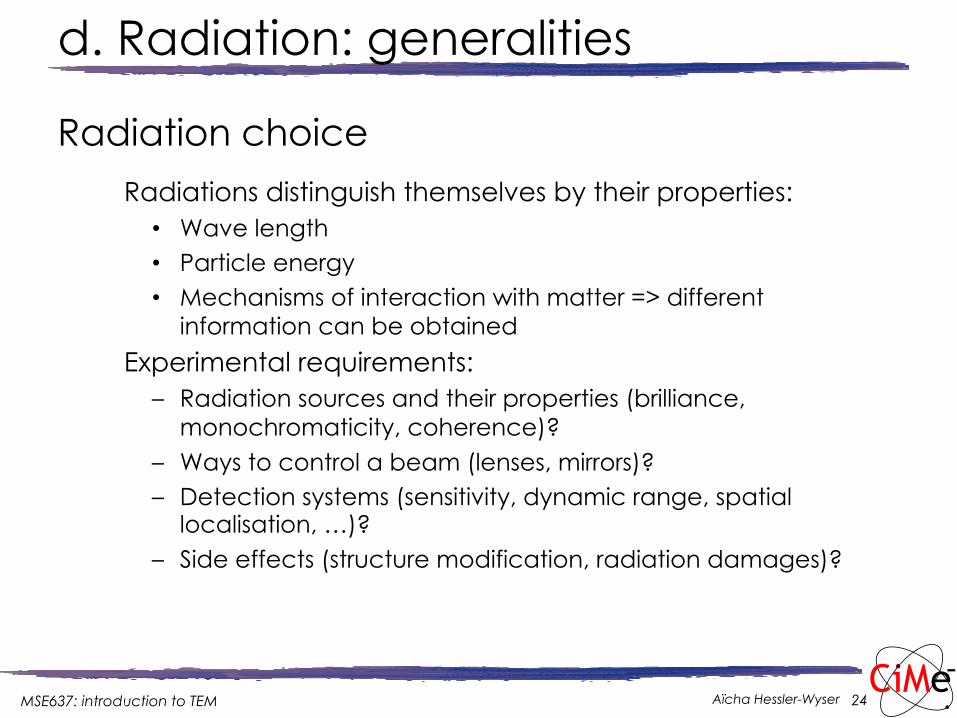
d. Radiation: generalities
Radiation choice
Radiations distinguish themselves by their properties: • Wave length • Particle energy • Mechanisms of interaction with matter => different
information can be obtained
Experimental requirements: – Radiation sources and their properties (brilliance,
monochromaticity, coherence)? – Ways to control a beam (lenses, mirrors)? – Detection systems (sensitivity, dynamic range, spatial
localisation, …)? – Side effects (structure modification, radiation damages)?

Aïcha Hessler-Wyser 25 CiMe
MSE637: introduction to TEM
d. Radiation: wave length

Aïcha Hessler-Wyser 26 CiMe
MSE637: introduction to TEM
d. Radiation: generalities
Electron incident onto a bulk material Electron radiation
• Secondary electrons (SE): electrons ejected from material at low energy (5 to 50 eV).
• Back scattered electrons (BSE): incident electrons that are successively diffused and leave the sample: they are at high energy, close to initial energy E0.
• Auger Electrons: ejected electrons with an energy characteristic from the target atoms.
Electromagnetic radiation
• X rays with continuous energy, resulting from desceleration of incident electrons ("Bremstrahlung" or "slowing down radiation").
• X rays with energy characteristic from the target atoms. • Cathodoluminescence: Visible radiation mainly emitted by
isolating or semi-conducting materials.

Aïcha Hessler-Wyser 27 CiMe
MSE637: introduction to TEM
e. a little about diffraction
Interaction of electrons with the sample
Specimen
Inc
ide
nt
be
am
Auger electrons
Backscattered electrons BSE
secondary electrons SE Characteristic
X-rays
visible light
“absorbed” electrons electron-hole pairs
elastically scattered electrons
dire
ct
be
am
inelastically scattered electrons
Bremsstrahlung X-rays
1-100 nm

Aïcha Hessler-Wyser 28 CiMe
MSE637: introduction to TEM
e. Electron-matter interaction
Elastic diffusion
Incident electron
Diffused electron
ϑ
No energy transfer Low angle diffusion: Coulomb interaction with the electron cloud. High angle diffusion, or back scattering: Coulomb interaction with nucleus. Atom is not ionised.
Incident electron
Back scattered electron
Rutherford diffusion

Aïcha Hessler-Wyser 29 CiMe
MSE637: introduction to TEM
e. Electron-matter interaction
Inelastic diffusion
Incident electron Secondary
electron
Diffused electron
An incident electron ejects a bound electron then changes direction, with an energy lowered by the electron bound energy. The ejected electron, of low energy, is called secondary electron SE. The incident electron can be slowed down by Coulomb interaction with the nucleus. In the case of inelastic interaction, there is energy transfer, and the target atom can be ionised.
Incident electron
Diffused electron
ϑ
X ray (Bremstrahlung)

Aïcha Hessler-Wyser 30 CiMe
MSE637: introduction to TEM
e. Electron-matter interaction
Electron-holes creation: An incident electron onto a semiconductor can excite a valence electron to the conduction band, creating an electron-hole pair.
Cathodoluminescence: The excited electron recombines with its hole, emitting a photon with the gap energy, in the visible. This technique allows to put forward the defects that modify the gap energy.
Egap
Bande de conduction
Bande de valence
Electron incident
Egap
Bande de conduction
Bande de valence
Bande de conduction
Bande de valence
Electron avec perte d'énergie
Eg =hν

Aïcha Hessler-Wyser 31 CiMe
MSE637: introduction to TEM
e. Electron-matter interaction
Interaction with plasmons
Plasmons are collective oscillations of free electrons that occur when an electron goes through the free electron "gaz".
Plasmon energy depends on the free electron density, the latter changes with the atomic numer Z. The plasmon excitation induces thus an energy loss of the incident electron, which is chemically dependent on the sample.

Aïcha Hessler-Wyser 32 CiMe
MSE637: introduction to TEM
e. Electron-matter interaction
Interaction with phonons
Phonons are collective atom oscillations in a cristal. These are equivalent to a sample heating.
The electrons that excite phonons loose energy < 0.1 eV, but can be diffused at high angle.
No usefull information can be exctracted from phonons.

Aïcha Hessler-Wyser 33 CiMe
MSE637: introduction to TEM
e. Electron-matter interaction
Electron absorption – atom displacement ("knock on") – chemical bound breaking, – charge collective oscillation excitation (plasmons) – lattice atom vibrations (phonons) – excitation of surface electronic level (transition valence/
conduction,...) – core atomic level excitation (ionisation) – Bremsstrahlung radiation – the relative impact of these various interaction mechanisms varies
with the type of material (no simple modelling of absorption)

Aïcha Hessler-Wyser 34 CiMe
MSE637: introduction to TEM
e. Electron-matter interaction
Thickness needed to absorb 99% of a radiation for different elements
Element (specific masse)
4-Be 1.84 g/cm3
13-Al 2.7 g/cm3
29-Cu 8.93 g/cm3
82-Pb 11.3 g/cm3
X rays Cu-Kα λ=1.54 Å Mo-Kα λ=0.71 Å
16 mm 83 mm
0.35 mm 3.3 mm
0.10 mm 0.10 mm
0.017 mm 0.034 mm
Thermal neutrons λ≈1.08 Å
89 m ??
6 m
0.26 m
14 m
Electrons λ=0.037 Å à 100 kV λ=0.020 Å à 300 kV
39 µm
42 µm ~330 µm
11 µm
0.6 µm
Aïcha Hessler-Wyser 35 CiMe
MSE637: introduction to TEM
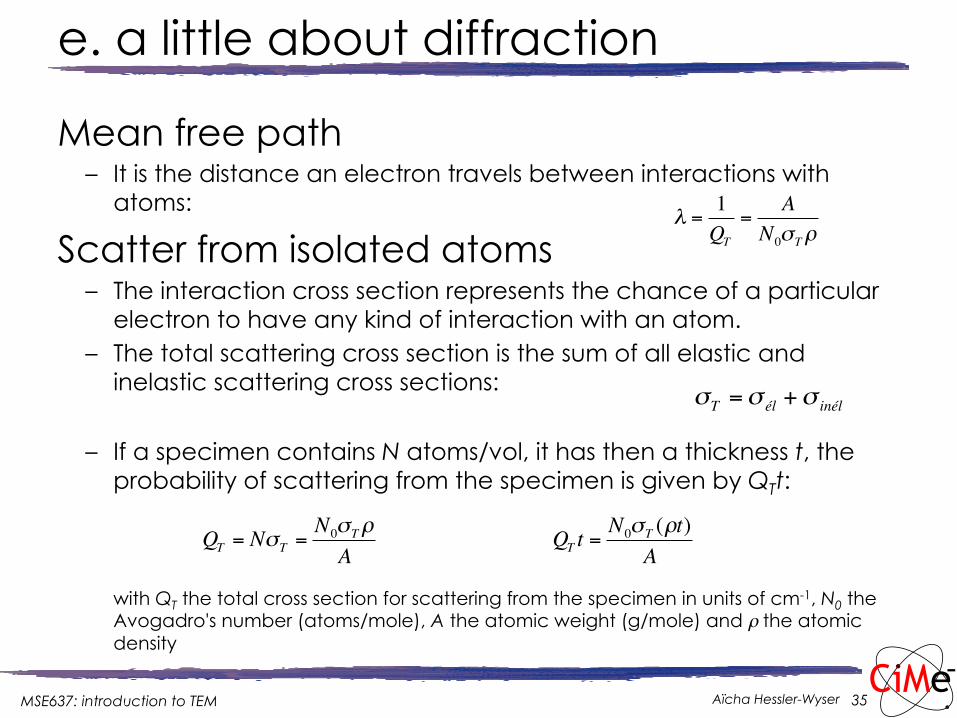
e. a little about diffraction
Mean free path – It is the distance an electron travels between interactions with
atoms:
Scatter from isolated atoms – The interaction cross section represents the chance of a particular
electron to have any kind of interaction with an atom. – The total scattering cross section is the sum of all elastic and
inelastic scattering cross sections:
– If a specimen contains N atoms/vol, it has then a thickness t, the probability of scattering from the specimen is given by QTt:
with QT the total cross section for scattering from the specimen in units of cm-1, N0 the Avogadro's number (atoms/mole), A the atomic weight (g/mole) and ρ the atomic density
€
λ =1QT
=A
N0σTρ
€
σT =σ él +σ inél
€
QT = NσT =N0σTρA
€
QT t =N0σT (ρt)
A

Aïcha Hessler-Wyser 36 CiMe
MSE637: introduction to TEM
e. a little about diffraction
The atomic scattering factor An incident electron plane wave is given by:
€
ψ( r ) =ψ0 e2πi k ⋅ r
€
€
ψsc ( r ) =ψ0 f (ϑ ) e
2πi k ⋅ r
r
When it is scattered by a scattering centre, a spherical scattered wave is created, which has amplitude ψsc but the same phase: where f(θ) is the atomic scattering factor, k the wave vectors of the incident or scattered wave, and r the distance that the wave has propagated.

Aïcha Hessler-Wyser 37 CiMe
MSE637: introduction to TEM
e. a little about diffraction
The atomic scattering factor The incident electrons wave has a uniform intensity. Scattering within the specimen changes both the spatial and angular distribution of the emerging electrons. The spatial distribution (A) is indicated by the wavy line. The change in angular distribution (B) is shown by an incident beam of electrons being transformed into several forward-scattered beams.

Aïcha Hessler-Wyser 38 CiMe
MSE637: introduction to TEM
e. a little about diffraction
The atomic scattering factor The atomic scattering factor is related to the differential elastic scattering cross section by
– f(θ) is a measure of the amplitude of an electron wave scattered from an isolated atom.
– ⏐f(θ)⏐2 is proportional to the scattered intensity.
– f(θ) can be calculated from Schrödinger's equations, and we obtain the following description:
f(θ) depends on λ, θ and Z
€
f (ϑ ) 2 =dσdΩ
f (ϑ ) =1+ E0
m0c2
!
"#
$
%&
8π 2a0λ
sinϑ2
!
"
###
$
%
&&&
2
Z − fX( )

Aïcha Hessler-Wyser 39 CiMe
MSE637: introduction to TEM
e. a little about diffraction
The atomic scattering factor fn = 10+14 m fé 10+14 m
fX 10+14 m
(sinθ)/λ 0.1 0.5 0.1 0.5 0.1 0.5
1H -0.378 -0.378 4'530 890 0.23 0.02
63Cu 0.67 0.67 51'100 14'700 7.65 3.85
W 0.466 0.466 118'000 29'900 19.4 12
Atomic scattering factors for neutrons (independent of θ!), electrons and X rays, are a function of scattering angle and wave length λ [Å].
Tiré de L.H. Schwartz and J.B. Cohen, Diffraction from Materials fn : fé fX = 1 : 104 : 10

Aïcha Hessler-Wyser 40 CiMe
MSE637: introduction to TEM
e. a little about diffraction
[ ]∑=
⋅=
mailleatomesi
iimaille ifirrA rKπθπ 2exp)(]2exp[/1
with ri th position of an atom i: ri = xi a + yi b + zi c
and K = g: K = h a* + k b* + l c*
[ ]∑=
++=
mailleatomesi
iiiih lzkyhxif )(2expF kl π
The structure factor The amplitude (intensity) of a diffracted beam depends on the lattice structure and its atom positions: The structure factor is given by the sum of all scattering centres (the atoms) of the crystal that can scatter the incident wave:

Aïcha Hessler-Wyser 41 CiMe
MSE637: introduction to TEM
e. Resulting emission
Relaxation of an excited atom Characteristic X ray
Fluorescence X X ray energy caracteristic of the transition and thus of the element
Visible photon
Fluorescence Low transition energy, visible or UV photon is emitted
Auger electron
Emission Auger The relaxing process interacts with an elctron with a caracteristic energy

Aïcha Hessler-Wyser 42 CiMe
MSE637: introduction to TEM
e. Resulting emission
Relaxation of an excited atom

Aïcha Hessler-Wyser 43 CiMe
MSE637: introduction to TEM
e. Resulting emission
Emission RX: EDS spectrum (Energy Dispersive Spectroscopy)