data sheet maintenance/ (planed maintenance type ... · publication date: november 2006 sdb00123aeb...
TRANSCRIPT
1Publication date: November 2006 SDB00123AEB
DATA SHEET
NN12069APart No.
Package Code No. MLGA107-L2-0909
Mainten
ance/
Discon
tinued
Mainten
ance/D
iscont
inued
includ
es foll
owing
four P
roduct
lifecyc
le stag
e.
(planed
mainten
ance ty
pe, main
tenanc
e type,
planed
discon
tinued
typed,
discon
tinued
type)
NN12069A
2SDB00123AEB
ContentsOverview ……………………………………………………………………………………………………………. 3
Features …………………………………………………………………………………………………………….. 3
Applications ………………………………………………………………………………………………………… 3
Package ……………………………………………………………………………………………………………. 3
Type …………………………………...……………………………………………………………………………. 3
Block Diagram ………………...……………………………………………………………………………………. 4
Pin Arrangement ……………...……………………………………………………………………………………. 5
Pin Descriptions ……………………………………………………………………………………………………. 6
Absolute Maximum Ratings………………………………………………………………………………………… 9
Operating Supply Voltage Range …………..…………………………………………………………………… 9
Allowed Voltage Ranges ………………………………………………………………………………………… 10
Mainten
ance/
Discon
tinued
Mainten
ance/D
iscont
inued
includ
es foll
owing
four P
roduct
lifecyc
le stag
e.
(planed
mainten
ance ty
pe, main
tenanc
e type,
planed
discon
tinued
typed,
discon
tinued
type)
NN12069A
3SDB00123AEB
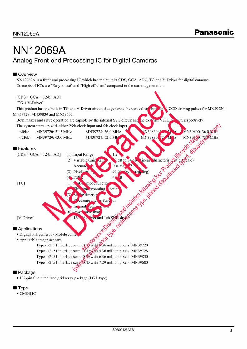
NN12069AAnalog Front-end Processing IC for Digital Cameras
OverviewNN12069A is a front-end processing IC which has the built-in CDS, GCA, ADC, TG and V-Driver for digital cameras.Concepts of IC’s are "Easy to use" and "High efficient" compared to the current generation.
[CDS + GCA + 12-bit AD][TG + V-Driver]This product has the built-in TG and V-Driver circuit that generate the vertical and horizontal CCD-driving pulses for MN39720,
MN39728, MN39830 and MN39600. Both master and slave operation are capable by the internal SSG circuit and the external VD/HD input, respectively.The system starts up with either 2fck clock input and fck clock input.
<fck> MN39720: 31.5 MHz MN39728: 36.0 MHz MN39830: 36.0 MHz MN39600: 36.0 MHz<2fck> MN39720: 63.0 MHz MN39728: 72.0 MHz MN39830: 72.0 MHz MN39600: 72.0 MHz
Features[CDS + GCA + 12-bit AD] (1) Input Range : 1.2 V
(2) Variable Gain Range : –2 dB to 34 dB (Linear Characteristic at dB scale)Accuracy : less than 0.5 dB
(3) Pixel settling : 99.9% (by 1 sampling)(4) PSRR : 40 dB
[TG] (1) Motion mode function(2) Electronic zooming function(3) Strobe function(4) Electronic shutter function(5) Internal SSG function(6) Power save mode
[V-Driver] (1) 13ch V-driver and 1ch SUB-driver .
ApplicationsDigital still cameras / Mobile camerasApplicable image sensors
Type-1/2. 51 interlace scan CCD with 5.36 million pixels: MN39720 Type-1/2. 51 interlace scan CCD with 5.36 million pixels: MN39728 Type-1/2. 51 interlace scan CCD with 6.36 million pixels: MN39830 Type-1/2. 51 interlace scan CCD with 7.29 million pixels: MN39600
Package107-pin fine pitch land grid array package (LGA type)
TypeCMOS IC
Mainten
ance/
Discon
tinued
Mainten
ance/D
iscont
inued
includ
es foll
owing
four P
roduct
lifecyc
le stag
e.
(planed
mainten
ance ty
pe, main
tenanc
e type,
planed
discon
tinued
typed,
discon
tinued
type)
NN12069A
4SDB00123AEB
Block Diagram
ADC
SERIAL
I/O
HDVDDRVSS
S/H
DRVDD
clamp
VrefL
TEST1
clamp
S/HTEST3
SSGSW
DVSS2
OV5AOV5B
OV3AOV5L OV3B
DVDD3
DVDD3
H1
VRT
OV6OV5R
OV2OV4
DCDET 2
CCDOUT
VRB
DCDET 1
CCD Timing Generator
XI
FCKSW
ADCLK
CPOB
DS2DS1
CPOB2
TEST2
CCD Vertical Driver
AN20112
DVSS3
DVSS3
OSUB
VL
EXADCLK
EXDS2
EXDS1
VHVHVM
D0 D1 D2 D3 D4 D5 D6 D7 D8 D9 D10 D11
RESET
DATA
DCLK
XO ClockGenerator
DVDD1
DVSS1
CS
CLKO
DVSS2
DVSS2
DVDD2
DVDD2
DVDD2
DVDD2
H2
H3
H4
STO
SUBSW
SHUT
OV3LOV1SOV3ROV1
VL
VM VHH
CH
1 to
CH
5
V1
to V
6, V
1S,
V3L
, V3R
, V
5L, V
5R
SUB
, SU
BC
NT
CLR
AFE + TGAN12069
PBLK
DVSS2
93
59
60
61
32
31
30
27
33
28
34
26
25
5
65
66
64
2
3
23
24
9 10 11 12 13 14 15 16 17 18 19 20 21 22 70 1 6362694
47
57
67
6
48
68
58
55
56
49
51
52
53
36
38
40
41
35
39
37
42
VrefH
DCCont
90 74 73 91 72 89 88 87 86 84 83 82 81 80 79 78 77 7685
71
92
GCAMP
+ –
VSS
VSS
VDD
VDD
CCDSW1
50
DVSS4
DVDD4
HL
R
44
45
43
46
VMSUB
75
CCDSW2
54
DCDET 3 29
Mainten
ance/
Discon
tinued
Mainten
ance/D
iscont
inued
includ
es foll
owing
four P
roduct
lifecyc
le stag
e.
(planed
mainten
ance ty
pe, main
tenanc
e type,
planed
discon
tinued
typed,
discon
tinued
type)
NN12069A
5SDB00123AEB
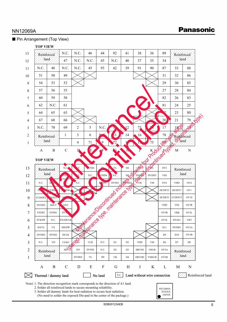
Pin Arrangement (Top View)
TOP VIEW
TOP VIEW
1
2
3
4
5
6
8
9
10
11
12
13
A B C D E F H J K L M NG
7
Reinforced land 4 71 9 13 15 75 77
1 3 6 N.C. 14 16 76 78
70 2 5 N.C. 12 73 74 18
67 68 66 20 21 79
64 65 63 22 23
62 N.C. 81 24 25
57 56 55 27 28
54 53 52 29 30 85
50 49 31 32 86
48 N.C. 45 93 39 91 90 33
47 N.C. N.C. 43 40 37 35 34
N.C. 46 44 41 38 36 89
Reinforced land
Reinforced land
Reinforced land
19N.C.
61
51
N.C.
80
84
88
N.C.
42
N.C.
92
72
11
10
60 59 58 82 26 83
69 17
87N.C.
Reinforced land DVDD2 VL D0 D4 DRVDD VMSUB OV5B
HD XO DVSS2 N.C. D5 DRVSS OSUB OV5A
VD XI CLR N.C. D3 VHH VM D7
DVDD2 DVSS2 DCLK D9 D10 OV3B
DATA CS SSGSW D11 DVDD1
FCKSW N.C. OV5L DVSS1 VRT
DVDD2 SHUT STO VDD VSS
CCDSW2 TEST3 TEST2 DCDET3 CCDOUT OV1S
CCDSW1 SUBSW DCDET2 DCDET1 OV1
DVSS2 N.C. R RESET DVDD3 VH VM VDD
DVDD2 N.C. N.C. DVDD4 H3 DVSS3 DVDD3 VSS
N.C. DVSS4 HL H4 H2 H1 OV2
Reinforced land
Reinforced land
Reinforced land
A B C D E F H J K L M N
1
2
3
4
5
6
8
9
10
11
12
13
D8N.C.
EXADCLK
TEST1
N.C.
OV3A
OV3R
OV4
N.C.
DVSS3
N.C.
VL
VH
D2
D1
G
EXDS2 EXDS1 DVSS27 OV5R VRB OV3L
CLKO D6
OV6N.C.
N.C.Thermal / dummy land No land Land without wire connection
NN12069AXXXXXJAPAN
N.C.Thermal / dummy land No land Land without wire connection Reinforced land
Note) 1. The direction recognition mark corresponds to the direction of A1 land.2. Solder all reinforced lands to secure mounting reliability.3. Solder all dummy lands for heat radiation to secure heat radiation.
(No need to solder the exposed Die-pad in the center of the package.)
Mainten
ance/
Discon
tinued
Mainten
ance/D
iscont
inued
includ
es foll
owing
four P
roduct
lifecyc
le stag
e.
(planed
mainten
ance ty
pe, main
tenanc
e type,
planed
discon
tinued
typed,
discon
tinued
type)
NN12069A
6SDB00123AEB
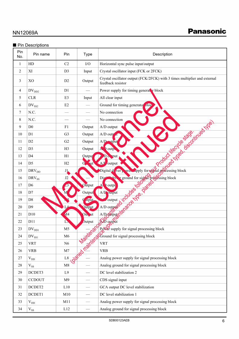
Pin Descriptions
L12
M11
M10
L10
M9
L9
M8
L8
M7
N6
M6
M5
L5
M4
L4
N3
M3
L3
J2
J1
H2
H1
H3
G2
G3
F1
—
—
E2
E3
D1
D2
D3
C2
Pin DescriptionTypePin namePin No.
Analog ground for signal processing block—VSS34
GCA output DC level stabilization—DCDET231
CDS signal input—CCDOUT30
DC level stabilization 2—DCDET329
Ground for signal processing block—DVSS124
Power supply for signal processing block—DVDD123
A/D outputOutputD1122
A/D outputOutputD1021
A/D outputOutputD920
A/D outputOutputD819
A/D outputOutputD718
A/D outputOutputD617
Analog power supply for signal processing block—VDD33
DC level stabilization 1—DCDET132
Analog ground for signal processing block—VSS28
Analog power supply for signal processing block—VDD27
VRB—VRB26
VRT—VRT25
Digital driver ground for signal processing block—DRVSS16
Digital driver power supply for signal processing block—DRVDD15
A/D outputOutputD514
A/D outputOutputD413
A/D outputOutputD312
A/D outputOutputD211
A/D outputOutputD110
A/D outputOutputD09
No connection—N.C.8
No connection—N.C.7
Ground for timing generator block—DVSS26
All clear inputInputCLR5
Power supply for timing generator block—DVDD24
Crystal oscillator output (FCK/2FCK) with 3 times multiplier and external feedback resistorOutputXO3
Crystal oscillator input (FCK or 2FCK)InputXI2
Horizontal sync pulse input/outputI/OHD1
Mainten
ance/
Discon
tinued
Mainten
ance/D
iscont
inued
includ
es foll
owing
four P
roduct
lifecyc
le stag
e.
(planed
mainten
ance ty
pe, main
tenanc
e type,
planed
discon
tinued
typed,
discon
tinued
type)
NN12069A
7SDB00123AEB
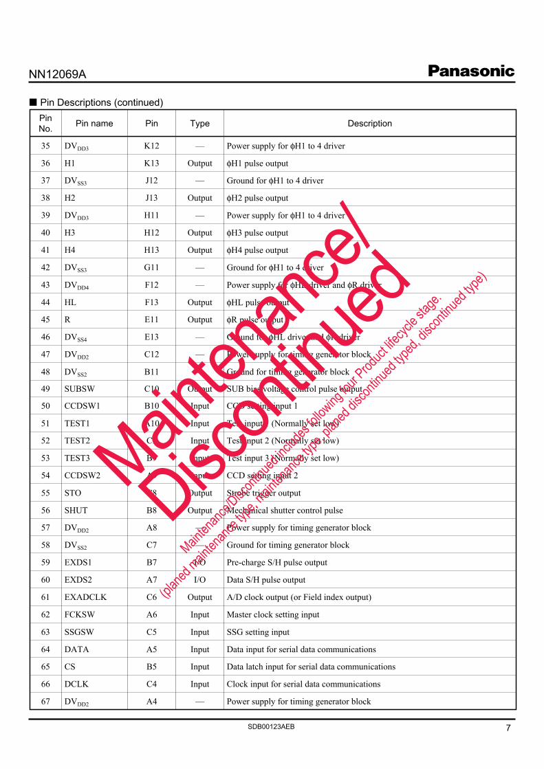
Pin Descriptions (continued)
Power supply for φH1 to 4 driver—K12DVDD335
A4
C4
B5
A5
C5
A6
C6
A7
B7
C7
A8
B8
C8
A9
B9
C9
A10
B10
C10
B11
C12
E13
E11
F13
F12
G11
H13
H12
H11
J13
J12
K13
Pin DescriptionTypePin namePin No.
Clock input for serial data communicationsInputDCLK66
Data latch input for serial data communicationsInputCS65
Data input for serial data communicationsInputDATA64
Pre-charge S/H pulse outputI/OEXDS159
Ground for timing generator block—DVSS258
Power supply for timing generator block—DVDD257
Mechanical shutter control pulseOutputSHUT56
Strobe trigger outputOutputSTO55
CCD setting input 2InputCCDSW254
Test input 3 (Normally set low)InputTEST353
Test input 2 (Normally set low)InputTEST252
Power supply for timing generator block—DVDD267
SSG setting inputInputSSGSW63
Master clock setting inputInputFCKSW62
A/D clock output (or Field index output)OutputEXADCLK61
Data S/H pulse outputI/OEXDS260
Test input 1 (Normally set low)InputTEST151
CCD setting input 1InputCCDSW150
SUB bias voltage control pulse outputOutputSUBSW49
Ground for timing generator block—DVSS248
Power supply for timing generator block—DVDD247
Ground for φHL driver and φR driver—DVSS446
φR pulse outputOutputR45
φHL pulse outputOutputHL44
Power supply for φHL driver and φR driver—DVDD443
Ground for φH1 to 4 driver—DVSS342
φH4 pulse outputOutputH441
φH3 pulse outputOutputH340
Power supply for φH1 to 4 driver—DVDD339
φH2 pulse outputOutputH238
Ground for φH1 to 4 driver—DVSS337
φH1 pulse outputOutputH136
Mainten
ance/
Discon
tinued
Mainten
ance/D
iscont
inued
includ
es foll
owing
four P
roduct
lifecyc
le stag
e.
(planed
mainten
ance ty
pe, main
tenanc
e type,
planed
discon
tinued
typed,
discon
tinued
type)
NN12069A
8SDB00123AEB
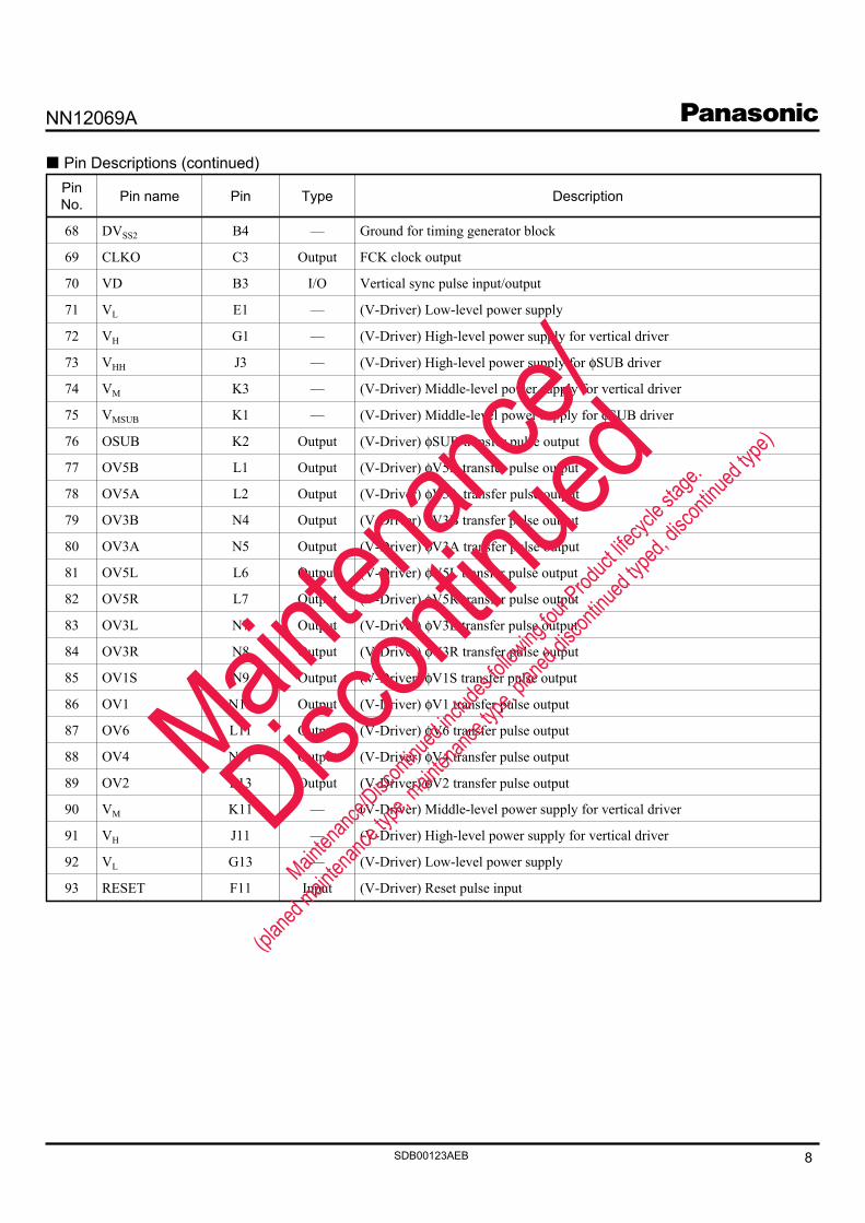
Pin Descriptions (continued)
Ground for timing generator block—B4DVSS268
FCK clock outputOutputC3CLKO69
Vertical sync pulse input/outputI/OB3VD70
F11
G13
J11
K11
L13
N11
L11
N10
N9
N8
N7
L7
L6
N5
N4
L2
L1
K2
K1
K3
J3
G1
E1
Pin DescriptionTypePin namePin No.
(V-Driver) Reset pulse inputInputRESET93
(V-Driver) Low-level power supply—VL92
(V-Driver) High-level power supply for vertical driver—VH91
(V-Driver) Middle-level power supply for vertical driver—VM90
(V-Driver) φV2 transfer pulse outputOutputOV289
(V-Driver) φV4 transfer pulse outputOutputOV488
(V-Driver) φV6 transfer pulse outputOutputOV687
(V-Driver) φV1 transfer pulse outputOutputOV186
(V-Driver) φV1S transfer pulse outputOutputOV1S85
(V-Driver) φV3R transfer pulse outputOutputOV3R84
(V-Driver) φV3L transfer pulse outputOutputOV3L83
(V-Driver) φV5R transfer pulse outputOutputOV5R82
(V-Driver) φV5L transfer pulse outputOutputOV5L81
(V-Driver) φV3A transfer pulse outputOutputOV3A80
(V-Driver) φV3B transfer pulse outputOutputOV3B79
(V-Driver) φV5A transfer pulse outputOutputOV5A78
(V-Driver) φV5B transfer pulse outputOutputOV5B77
(V-Driver) φSUB transfer pulse outputOutputOSUB76
(V-Driver) Middle-level power supply for φSUB driver—VMSUB75
(V-Driver) Middle-level power supply for vertical driver—VM74
(V-Driver) High-level power supply for φSUB driver—VHH73
(V-Driver) High-level power supply for vertical driver—VH72
(V-Driver) Low-level power supply—VL71
Mainten
ance/
Discon
tinued
Mainten
ance/D
iscont
inued
includ
es foll
owing
four P
roduct
lifecyc
le stag
e.
(planed
mainten
ance ty
pe, main
tenanc
e type,
planed
discon
tinued
typed,
discon
tinued
type)
NN12069A
9SDB00123AEB
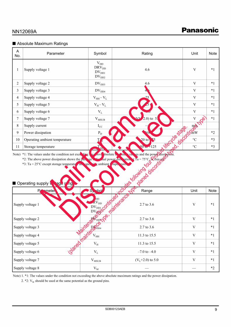
Absolute Maximum Ratings
Operating supply voltage range
Note) *1: The values under the condition not exceeding the above absolute maximum ratings and the power dissipation.*2: The above power dissipation shows the package individual power dissipation at Ta = 75°C, in free-air.*3: Ta = 25°C except storage temperature and operating ambient temperature .
*1V2.7 to 3.6DVDD4Supply voltage 3
*2
*1
*1
*1
*1
*1
*1
Note
—
V
V
V
V
V
V
Unit
(VL+2.0) to 5.0VMSUBSupply voltage 7
–7.0 to –4.0VLSupply voltage 6
11.3 to 15.5VHSupply voltage 5
—VMSupply voltage 8
11.3 to 15.5VHH Supply voltage 4
2.7 to 3.6DVDD3Supply voltage 2
2.7 to 3.6
VDDDRVDDDVDD1DVDD2
Supply voltage 1
RangeSymbolParameter
Note) 1. *1: The values under the condition not exceeding the above absolute maximum ratings and the power dissipation.2. *2: VM should be used at the same potential as the ground pins.
*1V4.6DVDD4Supply voltage 33
*3°C–50 to +125TstgStorage temperature11
*3°C–20 to +75ToprOperating ambient temperature10
*2mW268PDPower dissipation9
mA—ICCSupply current8
*1V(VL+2.0) to 5.5VMSUBSupply voltage 77
NoteUnitRatingSymbolParameterA No.
*1V4.6DVDD3Supply voltage 22
*1V–9.0VLSupply voltage 66
*1V25VH – VLSupply voltage 55
*1V25VHH – VLSupply voltage 44
*1V4.6
VDDDRVDDDVDD1DVDD2
Supply voltage 11
Mainten
ance/
Discon
tinued
Mainten
ance/D
iscont
inued
includ
es foll
owing
four P
roduct
lifecyc
le stag
e.
(planed
mainten
ance ty
pe, main
tenanc
e type,
planed
discon
tinued
typed,
discon
tinued
type)
NN12069A
10SDB00123AEB
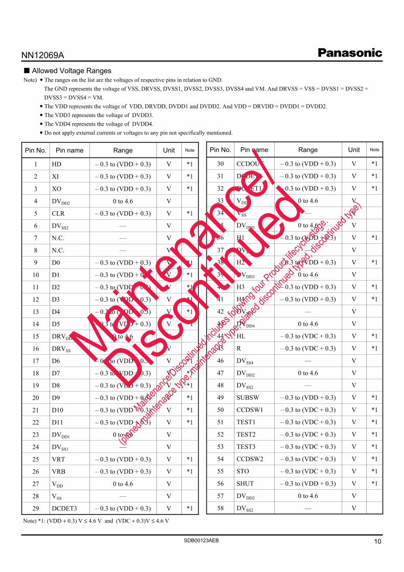
Note) *1: (VDD + 0.3) V ≤ 4.6 V and (VDC + 0.3)V ≤ 4.6 V
Allowed Voltage Ranges Note) The ranges on the list are the voltages of respective pins in relation to GND.
The GND represents the voltage of VSS, DRVSS, DVSS1, DVSS2, DVSS3, DVSS4 and VM. And DRVSS = VSS = DVSS1 = DVSS2 =DVSS3 = DVSS4 = VM.The VDD represents the voltage of VDD, DRVDD, DVDD1 and DVDD2. And VDD = DRVDD = DVDD1 = DVDD2.The VDD3 represents the voltage of DVDD3.The VDD4 represents the voltage of DVDD4.Do not apply external currents or voltages to any pin not specifically mentioned.
*1V– 0.3 to (VDD + 0.3)D819
*1V– 0.3 to (VDD + 0.3)D920
*1V– 0.3 to (VDD + 0.3)D1021
*1V– 0.3 to (VDD + 0.3)D1122
V0 to 4.6DVDD123
V—DVSS124
*1V– 0.3 to (VDD + 0.3)VRT25
*1V– 0.3 to (VDD + 0.3)VRB26
V0 to 4.6VDD27
V—VSS28
*1V– 0.3 to (VDD + 0.3)DCDET329
*1V– 0.3 to (VDD + 0.3)D312
*1V– 0.3 to (VDD + 0.3)D413
*1V– 0.3 to (VDD + 0.3)D514
V0 to 4.6DRVDD15
V—DRVSS16
*1V– 0.3 to (VDD + 0.3)D617
*1V– 0.3 to (VDD + 0.3)D718
*1V– 0.3 to (VDD + 0.3)D211
*1V– 0.3 to (VDD + 0.3)D110
*1V– 0.3 to (VDD + 0.3)D09
V—N.C.8
V—N.C.7
V—DVSS26
*1V– 0.3 to (VDD + 0.3)XI2
– 0.3 to (VDD + 0.3)HD
NoteUnitRangePin namePin No.
*1V– 0.3 to (VDD + 0.3)CLR5
V0 to 4.6DVDD24
*1V– 0.3 to (VDD + 0.3)XO3
*1V1
V—DVSS248
*1V– 0.3 to (VDD + 0.3)SUBSW49
*1V– 0.3 to (VDC + 0.3)CCDSW150
*1V– 0.3 to (VDC + 0.3)TEST151
*1V– 0.3 to (VDC + 0.3)TEST252
*1V– 0.3 to (VDC + 0.3)TEST353
*1V– 0.3 to (VDC + 0.3)CCDSW254
*1V– 0.3 to (VDC + 0.3)STO55
*1V– 0.3 to (VDD + 0.3)SHUT56
V0 to 4.6DVDD257
V—DVSS258
*1V– 0.3 to (VDD + 0.3)H441
V—DVSS342
V0 to 4.6DVDD443
*1V– 0.3 to (VDC + 0.3)HL44
*1V– 0.3 to (VDC + 0.3)R45
V—DVSS446
V0 to 4.6DVDD247
*1V– 0.3 to (VDD + 0.3)H340
V0 to 4.6DVDD339
*1V– 0.3 to (VDD + 0.3)H238
V—DVSS337
*1V– 0.3 to (VDD + 0.3)H136
V0 to 4.6DVDD335
*1V– 0.3 to (VDD + 0.3)DCDET231
– 0.3 to (VDD + 0.3)CCDOUT
NoteUnitRangePin namePin No.
V—VSS34
V0 to 4.6VDD33
*1V– 0.3 to (VDD + 0.3)DCDET132
*1V30
Mainten
ance/
Discon
tinued
Mainten
ance/D
iscont
inued
includ
es foll
owing
four P
roduct
lifecyc
le stag
e.
(planed
mainten
ance ty
pe, main
tenanc
e type,
planed
discon
tinued
typed,
discon
tinued
type)
NN12069A
11SDB00123AEB
*1V– 0.3 to (VDD + 0.3)VD70
V–9.0 to 0VL71
V0 to 16.0VH72
V0 to 16.0VHH73
V—VM74
V(VL+2.0) to 5.5VMSUB75
*1V– 0.3 to (VDD + 0.3)CLKO69
V—DVSS268
V0 to 4.6DVDD267
*1V– 0.3 to (VDD + 0.3)DCLK66
*1V– 0.3 to (VDD + 0.3)CS65
*1V– 0.3 to (VDD + 0.3)DATA64
*1V– 0.3 to (VDD + 0.3)EXDS260
– 0.3 to (VDD + 0.3)EXDS1
NoteUnitRangePin namePin No.
*1V– 0.3 to (VDD + 0.3)SSGSW63
*1V– 0.3 to (VDD + 0.3)FCKSW62
*1V– 0.3 to (VDD + 0.3)EXADCLK61
*1V59
Note) *1: (VDD + 0.3) V ≤ 4.6 V and (VDC + 0.3)V ≤ 4.6 V *2: Do not apply the voltages or the currents to the pins from external.
*2V—OSUB76
*2V—OV5B77
*2V—OV5A78
*2V—OV3B79
*2V—OV3A80
*2V—OV5L81
*2V—OV5R82
*2V—OV3L83
*2V—OV3R84
*2V—OV1S85
*2V—OV186
*2V—OV687
*1V– 0.3 to (VDD + 0.3)RESET93
*2V—OV289
—OV4
NoteUnitRangePin namePin No.
V–9.0 to 0VL92
V0 to 16.0VH91
V—VM90
*2V88
Allowed Voltage Ranges (continued)Note) The ranges on the list are the voltages of respective pins in relation to GND.
The GND represents the voltage of VSS, DRVSS, DVSS1, DVSS2, DVSS3, DVSS4 and VM. And DRVSS = VSS = DVSS1 = DVSS2 =DVSS3 = DVSS4 = VM.The VDD represents the voltage of VDD, DRVDD, DVDD1 and DVDD2. And VDD = DRVDD = DVDD1 = DVDD2.The VDD3 represents the voltage of DVDD3.The VDD4 represents the voltage of DVDD4.Do not apply external currents or voltages to any pin not specifically mentioned.
Mainten
ance/
Discon
tinued
Mainten
ance/D
iscont
inued
includ
es foll
owing
four P
roduct
lifecyc
le stag
e.
(planed
mainten
ance ty
pe, main
tenanc
e type,
planed
discon
tinued
typed,
discon
tinued
type)
Request for your special attention and precautions in using the technical information andsemiconductors described in this book
(1)If any of the products or technical information described in this book is to be exported or provided to non-residents, the laws and regulations of the exporting country, especially, those with regard to security export control, must be observed.
(2)The technical information described in this book is intended only to show the main characteristics and application circuit examples of the products, and no license is granted under any intellectual property right or other right owned by our company or any other company. Therefore, no responsibility is assumed by our company as to the infringement upon any such right owned by any other company which may arise as a result of the use of technical information described in this book.
(3)The products described in this book are intended to be used for standard applications or general electronic equipment (such as office equipment, communications equipment, measuring instruments and household appliances). Consult our sales staff in advance for information on the following applications:� Special applications (such as for airplanes, aerospace, automobiles, traffic control equipment, combustion equipment, life support
systems and safety devices) in which exceptional quality and reliability are required, or if the failure or malfunction of the prod-ucts may directly jeopardize life or harm the human body.� Any applications other than the standard applications intended.
(4)The products and product specifications described in this book are subject to change without notice for modification and/or im-provement. At the final stage of your design, purchasing, or use of the products, therefore, ask for the most up-to-date Product Standards in advance to make sure that the latest specifications satisfy your requirements.
(5)When designing your equipment, comply with the range of absolute maximum rating and the guaranteed operating conditions (operating power supply voltage and operating environment etc.). Especially, please be careful not to exceed the range of absolute maximum rating on the transient state, such as power-on, power-off and mode-switching. Otherwise, we will not be liable for any defect which may arise later in your equipment.
Even when the products are used within the guaranteed values, take into the consideration of incidence of break down and failure mode, possible to occur to semiconductor products. Measures on the systems such as redundant design, arresting the spread of fire or preventing glitch are recommended in order to prevent physical injury, fire, social damages, for example, by using the products.
(6)Comply with the instructions for use in order to prevent breakdown and characteristics change due to external factors (ESD, EOS, thermal stress and mechanical stress) at the time of handling, mounting or at customer's process. When using products for which damp-proof packing is required, satisfy the conditions, such as shelf life and the elapsed time since first opening the packages.
(7)This book may be not reprinted or reproduced whether wholly or partially, without the prior written permission of Matsushita Electric Industrial Co., Ltd.
Mainten
ance/
Discon
tinued
Mainten
ance/D
iscont
inued
includ
es foll
owing
four P
roduct
lifecyc
le stag
e.
(planed
mainten
ance ty
pe, main
tenanc
e type,
planed
discon
tinued
typed,
discon
tinued
type)