data brief - stm32u585xx - ultra-low-power arm® cortex
TRANSCRIPT

For further information contact your local STMicroelectronics sales office.
February 2021 DB3734 Rev 2 1/170
STM32U585xx
Ultra-low-power Arm® Cortex®-M33 32-bit MCU+TrustZone®+FPU, 240 DMIPS, up to 2 MB Flash memory, 786 KB SRAM, SMPS
Data brief
Features
Includes ST state-of-the-art patented technology
Ultra-low-power with FlexPowerControl
• 1.71 V to 3.6 V power supply
• –40 °C to +85/125 °C temperature range
• Low-power background autonomous mode (LPBAM): autonomous peripherals with DMA, functional down to Stop 2 mode
• VBAT mode: supply for RTC, 32 x 32-bit backup registers and 2-Kbyte backup SRAM
• 110 nA Shutdown mode (24 wakeup pins)
• 300 nA Standby mode (24 wakeup pins)
• 475 nA Standby mode with RTC
• 1.7 μA Stop 3 mode with 16-Kbyte SRAM
• 3.1 µA Stop 3 mode with full SRAM
• 3.4 µA Stop 2 mode with 16-Kbyte SRAM
• 6.6 µA Stop 2 mode with full SRAM
• 19.5 μA/MHz Run mode @ 3.3 V
Core
• Arm® 32-bit Cortex®-M33 CPU with TrustZone® and FPU
ART Accelerator
• 8-Kbyte instruction cache allowing 0-wait-state execution from Flash and external memories: up to 160 MHz, MPU, 240 DMIPS and DSP
• 4-Kbyte data cache for external memories
Power management
• Embedded regulator (LDO) and SMPS step-down converter supporting switch on-the-fly and voltage scaling
Benchmarks
• 1.5 DMIPS/MHz (Drystone 2.1)
• 651 CoreMark® (4.07 CoreMark®/MHz)
• 535 ULPMark™-CP
• 149 ULPMark™-PP
• 58.2 ULPMark™-CM
• 133000 SecureMark™-TLS
Memories
• 2-Mbyte Flash memory with ECC, 2 banks read-while-write, including 512 Kbytes with 100 kcycles
• 786-Kbyte SRAM with ECC OFF or 722-Kbyte SRAM including up to 322-Kbyte SRAM with ECC ON
• External memory interface supporting SRAM, PSRAM, NOR, NAND and FRAM memories
• 2 Octo-SPI memory interfaces
Security and cryptography
• Arm® TrustZone® and securable I/Os, memories and peripherals
• Flexible life cycle scheme with RDP and password protected debug
• Root of trust thanks to unique boot entry and secure hide protection area (HDP)
• SFI (secure firmware installation) thanks to embedded RSS (root secure services)
• Secure data storage with hardware unique key (HUK)
• Secure firmware upgrade support with TF-M
LQFP48 (7 x 7 mm)LQFP64 (10 x 10 mm)
LQFP100 (14 x 14 mm)LQFP144 (20 x 20 mm)
UFQFPN48(7 x 7 mm)
WLCSP90(4.2 x 3.95 mm)
UFBGA132(7 x 7 mm)UFBGA169(7 x 7 mm)
www.st.com
INAC
TIVE
- IN
ACTI
VE -
INAC
TIVE
STM32U585xx
2/170 DB3734 Rev 2
• 2 AES coprocessors including one with DPA resistance
• Public key accelerator, DPA resistant
• On-the-fly decryption of Octo-SPI external memories
• HASH hardware accelerator
• True random number generator, NIST SP800-90B compliant
• 96-bit unique ID
• 512-byte OTP (one-time programmable)
• Active tampers
Clock management
• 4 to 50 MHz crystal oscillator
• 32 kHz crystal oscillator for RTC (LSE)
• Internal 16 MHz factory-trimmed RC (± 1 %)
• Internal low-power 32 kHz RC (± 5 %)
• 2 internal multispeed 100 kHz to 48 MHz oscillators, including one auto-trimmed by LSE (better than ± 0.25 % accuracy)
• Internal 48 MHz with clock recovery
• 3 PLLs for system clock, USB, audio, ADC
General-purpose input/outputs
• Up to 136 fast I/Os with interrupt capability most 5V-tolerant and up to 14 I/Os with independent supply down to 1.08 V
Up to 17 timers and 2 watchdogs
• 19 timers: 2 16-bit advanced motor-control, 4 32-bit, 5 16-bit, 4 low-power 16-bit (available in Stop mode), 2 SysTick timers and 2 watchdogs
• RTC with hardware calendar and calibration
Up to 22 communication peripherals
• 1 USB Type-C™/USB power delivery controller
• 1 USB OTG 2.0 full-speed controller
• 2 SAIs (serial-audio interface)
• 4 I2C FM+(1 Mbit/s), SMBus/PMBus™
• 6 USARTs (ISO 7816, LIN, IrDA, modem)
• 3 SPIs (5x SPIs with the dual OCTOSPI)
• 1 CAN FD controller
• 2 SDMMC interfaces
• 1 multi-function digital filter (6 filters)+ 1 audio digital filter with sound-activity detection
• Parallel synchronous slave interface
16- and 4-channel DMA controllers, functional in Stop mode
Graphic features
• Chrom-ART Accelerator (DMA2D) for enhanced graphic content creation
• 1 digital camera interface
Mathematical co-processor
• CORDIC for trigonometric functions acceleration
• FMAC (filter mathematical accelerator)
Up to 24 capacitive sensing channels
• Support touch key, linear and rotary touch sensors
Rich analog peripherals (independent supply)
• 14-bit ADC 2.5-Msps, resolution up to 16 bits with hardware oversampling
• 12-bit ADC 2.5-Msps, with hardware oversampling, autonomous in Stop 2 mode
• 2 12-bit DAC, low-power sample and hold
• 2 operational amplifiers with built-in PGA
• 2 ultra-low-power comparators
CRC calculation unit
Debug• Development support: serial-wire debug
(SWD), JTAG, Embedded Trace Macrocell™ (ETM)
ECOPACK2 compliant packages
Table 1. Device summary
Reference Part numbers
STM32U585xxSTM32U585AI, STM32U585CI,STM32U585OI, STM32U585QI, STM32U585RI, STM32U585VI, STM32U585ZI
INAC
TIVE
- IN
ACTI
VE -
INAC
TIVE

DB3734 Rev 2 3/170
STM32U585xx Contents
6
Contents
1 Introduction . . . . . . . . . . . . . . . . . . . . . . . . . . . . . . . . . . . . . . . . . . . . . . . . 9
2 Description . . . . . . . . . . . . . . . . . . . . . . . . . . . . . . . . . . . . . . . . . . . . . . . . 10
3 Functional overview . . . . . . . . . . . . . . . . . . . . . . . . . . . . . . . . . . . . . . . . 15
3.1 Arm Cortex-M33 core with TrustZone and FPU . . . . . . . . . . . . . . . . . . . . 15
3.2 ART Accelerator (ICACHE and DCACHE) . . . . . . . . . . . . . . . . . . . . . . . . 15
3.2.1 Instruction cache (ICACHE) . . . . . . . . . . . . . . . . . . . . . . . . . . . . . . . . . . 15
3.2.2 Data cache (DCACHE) . . . . . . . . . . . . . . . . . . . . . . . . . . . . . . . . . . . . . 16
3.3 Memory protection unit . . . . . . . . . . . . . . . . . . . . . . . . . . . . . . . . . . . . . . . 17
3.4 Embedded Flash memory . . . . . . . . . . . . . . . . . . . . . . . . . . . . . . . . . . . . 17
3.4.1 Flash memory protections when TrustZone activated . . . . . . . . . . . . . . 20
3.4.2 FLASH privilege protection . . . . . . . . . . . . . . . . . . . . . . . . . . . . . . . . . . 21
3.5 Embedded SRAMs . . . . . . . . . . . . . . . . . . . . . . . . . . . . . . . . . . . . . . . . . . 21
3.5.1 SRAMs TrustZone security . . . . . . . . . . . . . . . . . . . . . . . . . . . . . . . . . . 21
3.5.2 SRAMs privilege protection . . . . . . . . . . . . . . . . . . . . . . . . . . . . . . . . . . 21
3.6 TrustZone security architecture . . . . . . . . . . . . . . . . . . . . . . . . . . . . . . . . 21
3.6.1 TrustZone peripheral classification . . . . . . . . . . . . . . . . . . . . . . . . . . . . 23
3.6.2 Default TrustZone security state . . . . . . . . . . . . . . . . . . . . . . . . . . . . . . 23
3.7 Boot modes . . . . . . . . . . . . . . . . . . . . . . . . . . . . . . . . . . . . . . . . . . . . . . . 23
3.8 Global TrustZone controller (GTZC) . . . . . . . . . . . . . . . . . . . . . . . . . . . . . 26
3.9 Power supply management . . . . . . . . . . . . . . . . . . . . . . . . . . . . . . . . . . . 26
3.9.1 Power supply schemes . . . . . . . . . . . . . . . . . . . . . . . . . . . . . . . . . . . . . 27
3.9.2 Power supply supervisor . . . . . . . . . . . . . . . . . . . . . . . . . . . . . . . . . . . . 31
3.9.3 Reset mode . . . . . . . . . . . . . . . . . . . . . . . . . . . . . . . . . . . . . . . . . . . . . . 40
3.9.4 VBAT operation . . . . . . . . . . . . . . . . . . . . . . . . . . . . . . . . . . . . . . . . . . . 40
3.9.5 PWR TrustZone security . . . . . . . . . . . . . . . . . . . . . . . . . . . . . . . . . . . . 40
3.10 Peripheral interconnect matrix . . . . . . . . . . . . . . . . . . . . . . . . . . . . . . . . . 41
3.11 Reset and clock controller (RCC) . . . . . . . . . . . . . . . . . . . . . . . . . . . . . . . 41
3.11.1 RCC TrustZone security . . . . . . . . . . . . . . . . . . . . . . . . . . . . . . . . . . . . 44
3.12 Clock recovery system (CRS) . . . . . . . . . . . . . . . . . . . . . . . . . . . . . . . . . 44
3.13 General-purpose inputs/outputs (GPIOs) . . . . . . . . . . . . . . . . . . . . . . . . . 44
3.13.1 GPIOs TrustZone security . . . . . . . . . . . . . . . . . . . . . . . . . . . . . . . . . . . 44
INAC
TIVE
- IN
ACTI
VE -
INAC
TIVE

Contents STM32U585xx
4/170 DB3734 Rev 2
3.14 Low-power general-purpose inputs/outputs (LPGPIO) . . . . . . . . . . . . . . 45
3.14.1 LPGPIO TrustZone security . . . . . . . . . . . . . . . . . . . . . . . . . . . . . . . . . . 45
3.15 Multi-AHB bus matrix . . . . . . . . . . . . . . . . . . . . . . . . . . . . . . . . . . . . . . . . 45
3.16 General purpose direct memory access controller (GPDMA) . . . . . . . . . 45
3.17 Low-power direct memory access controller (LPDMA) . . . . . . . . . . . . . . 47
3.18 Chrom-ART Accelerator controller (DMA2D) . . . . . . . . . . . . . . . . . . . . . . 49
3.19 Interrupts and events . . . . . . . . . . . . . . . . . . . . . . . . . . . . . . . . . . . . . . . . 50
3.19.1 Nested vectored interrupt controller (NVIC) . . . . . . . . . . . . . . . . . . . . . . 50
3.19.2 Extended interrupt/event controller (EXTI) . . . . . . . . . . . . . . . . . . . . . . 50
3.20 Cyclic redundancy check calculation unit (CRC) . . . . . . . . . . . . . . . . . . . 51
3.21 CORDIC co-processor (CORDIC) . . . . . . . . . . . . . . . . . . . . . . . . . . . . . . 51
3.22 Filter math accelerator (FMAC) . . . . . . . . . . . . . . . . . . . . . . . . . . . . . . . . 51
3.23 Flexible static memory controller (FSMC) . . . . . . . . . . . . . . . . . . . . . . . . 52
3.23.1 LCD parallel interface . . . . . . . . . . . . . . . . . . . . . . . . . . . . . . . . . . . . . . 52
3.23.2 FSMC TrustZone security . . . . . . . . . . . . . . . . . . . . . . . . . . . . . . . . . . . 53
3.24 Octo-SPI interface (OCTOSPI) . . . . . . . . . . . . . . . . . . . . . . . . . . . . . . . . 53
3.24.1 OCTOSPI TrustZone security . . . . . . . . . . . . . . . . . . . . . . . . . . . . . . . . 54
3.25 OCTOSPI I/O manager (OCTOSPIM) . . . . . . . . . . . . . . . . . . . . . . . . . . . 54
3.26 Delay block (DLYB) . . . . . . . . . . . . . . . . . . . . . . . . . . . . . . . . . . . . . . . . . 54
3.27 Analog-to-digital converter (ADC1 and ADC4) . . . . . . . . . . . . . . . . . . . . . 54
3.27.1 Analog-to-digital converter 1 (ADC1) . . . . . . . . . . . . . . . . . . . . . . . . . . . 55
3.27.2 Analog-to-digital converter 4 (ADC4) . . . . . . . . . . . . . . . . . . . . . . . . . . . 57
3.27.3 Temperature sensor . . . . . . . . . . . . . . . . . . . . . . . . . . . . . . . . . . . . . . . . 58
3.27.4 Internal voltage reference (VREFINT) . . . . . . . . . . . . . . . . . . . . . . . . . . 59
3.27.5 VBAT battery voltage monitoring . . . . . . . . . . . . . . . . . . . . . . . . . . . . . . 59
3.28 Digital to analog converter (DAC) . . . . . . . . . . . . . . . . . . . . . . . . . . . . . . . 59
3.29 Voltage reference buffer (VREFBUF) . . . . . . . . . . . . . . . . . . . . . . . . . . . . 60
3.30 Comparators (COMP) . . . . . . . . . . . . . . . . . . . . . . . . . . . . . . . . . . . . . . . 60
3.31 Operational amplifier (OPAMP) . . . . . . . . . . . . . . . . . . . . . . . . . . . . . . . . 61
3.32 Multi-function digital filter (MDF) and audio digital filter (ADF) . . . . . . . . . 61
3.32.1 Multi-function digital filter (MDF) . . . . . . . . . . . . . . . . . . . . . . . . . . . . . . 61
3.32.2 Audio digital filter (ADF) . . . . . . . . . . . . . . . . . . . . . . . . . . . . . . . . . . . . . 63
3.33 Digital camera interface (DCMI) . . . . . . . . . . . . . . . . . . . . . . . . . . . . . . . . 65
3.34 Parallel synchronous slave interface (PSSI) . . . . . . . . . . . . . . . . . . . . . . 65
INAC
TIVE
- IN
ACTI
VE -
INAC
TIVE

DB3734 Rev 2 5/170
STM32U585xx Contents
6
3.35 Touch sensing controller (TSC) . . . . . . . . . . . . . . . . . . . . . . . . . . . . . . . . 65
3.36 True random number generator (RNG) . . . . . . . . . . . . . . . . . . . . . . . . . . 66
3.37 Secure advanced encryption standard hardware accelerator (SAES) and encryption standard hardware accelerator (AES) . . . . . . . . . . . . . . . 67
3.38 HASH hardware accelerator (HASH) . . . . . . . . . . . . . . . . . . . . . . . . . . . . 69
3.39 On-the-fly decryption engine (OTFDEC) . . . . . . . . . . . . . . . . . . . . . . . . . 70
3.40 Public key accelerator (PKA) . . . . . . . . . . . . . . . . . . . . . . . . . . . . . . . . . . 71
3.41 Timers and watchdogs . . . . . . . . . . . . . . . . . . . . . . . . . . . . . . . . . . . . . . . 71
3.41.1 Advanced-control timers (TIM1, TIM8) . . . . . . . . . . . . . . . . . . . . . . . . . 72
3.41.2 General-purpose timers (TIM2, TIM3, TIM4, TIM5, TIM15, TIM16, TIM17) . . . . . . . . . . . . . . . . . . . . . . . . . . . . . . . . . . . . . . . . . . . . . . . . . . 72
3.41.3 Basic timers (TIM6 and TIM7) . . . . . . . . . . . . . . . . . . . . . . . . . . . . . . . . 73
3.41.4 Low-power timers (LPTIM1, LPTIM2, LPTIM3, LPTIM4) . . . . . . . . . . . . 73
3.41.5 Infrared interface (IRTIM) . . . . . . . . . . . . . . . . . . . . . . . . . . . . . . . . . . . 74
3.41.6 Independent watchdog (IWDG) . . . . . . . . . . . . . . . . . . . . . . . . . . . . . . . 74
3.41.7 Window watchdog (WWDG) . . . . . . . . . . . . . . . . . . . . . . . . . . . . . . . . . 74
3.41.8 SysTick timer . . . . . . . . . . . . . . . . . . . . . . . . . . . . . . . . . . . . . . . . . . . . . 74
3.42 Real-time clock (RTC), tamper and backup registers . . . . . . . . . . . . . . . 74
3.42.1 Real-time clock (RTC) . . . . . . . . . . . . . . . . . . . . . . . . . . . . . . . . . . . . . . 74
3.42.2 Tamper and backup registers (TAMP) . . . . . . . . . . . . . . . . . . . . . . . . . . 75
3.43 Inter-integrated circuit interface (I2C) . . . . . . . . . . . . . . . . . . . . . . . . . . . . 77
3.44 Universal synchronous/asynchronous receiver transmitter (USART/UART) and low-power universal asynchronous receiver transmitter (LPUART) . 78
3.44.1 Universal synchronous/asynchronous receiver transmitter (USART/UART) . . . . . . . . . . . . . . . . . . . . . . . . . . . . . . . . . . . . . . . . . . . 78
3.44.2 Low-power universal asynchronous receiver transmitter (LPUART) . . . 80
3.45 Serial peripheral interface (SPI) . . . . . . . . . . . . . . . . . . . . . . . . . . . . . . . . 81
3.46 Serial audio interfaces (SAI) . . . . . . . . . . . . . . . . . . . . . . . . . . . . . . . . . . . 82
3.47 Secure digital input/output and MultiMediaCards interface (SDMMC) . . . 83
3.48 Controller area network (FDCAN) . . . . . . . . . . . . . . . . . . . . . . . . . . . . . . 84
3.49 USB on-the-go full-speed (OTG_FS) . . . . . . . . . . . . . . . . . . . . . . . . . . . . 85
3.50 USB Type-C /USB Power Delivery controller (UCPD) . . . . . . . . . . . . . . . 86
3.51 Development support . . . . . . . . . . . . . . . . . . . . . . . . . . . . . . . . . . . . . . . . 87
3.51.1 Serial-wire/JTAG debug port (SWJ-DP) . . . . . . . . . . . . . . . . . . . . . . . . . 87
3.51.2 Embedded Trace Macrocell . . . . . . . . . . . . . . . . . . . . . . . . . . . . . . . . . . 87
INAC
TIVE
- IN
ACTI
VE -
INAC
TIVE

Contents STM32U585xx
6/170 DB3734 Rev 2
4 Pinout, pin description and alternate functions . . . . . . . . . . . . . . . . . . 88
4.1 Pinout/ballout schematics . . . . . . . . . . . . . . . . . . . . . . . . . . . . . . . . . . . . . 88
4.2 Pin description . . . . . . . . . . . . . . . . . . . . . . . . . . . . . . . . . . . . . . . . . . . . 100
4.3 Alternate functions . . . . . . . . . . . . . . . . . . . . . . . . . . . . . . . . . . . . . . . . . 124
5 Package information . . . . . . . . . . . . . . . . . . . . . . . . . . . . . . . . . . . . . . . 142
5.1 UFQFPN48 package information . . . . . . . . . . . . . . . . . . . . . . . . . . . . . . 142
5.2 LQFP48 package information . . . . . . . . . . . . . . . . . . . . . . . . . . . . . . . . . 145
5.3 LQFP64 package information . . . . . . . . . . . . . . . . . . . . . . . . . . . . . . . . . 148
5.4 WLSCP90 package information . . . . . . . . . . . . . . . . . . . . . . . . . . . . . . . 151
5.5 LQFP100 package information . . . . . . . . . . . . . . . . . . . . . . . . . . . . . . . . 154
5.6 UFBGA132 package information . . . . . . . . . . . . . . . . . . . . . . . . . . . . . . 157
5.7 LQFP144 package information . . . . . . . . . . . . . . . . . . . . . . . . . . . . . . . . 160
5.8 UFBGA169 package information . . . . . . . . . . . . . . . . . . . . . . . . . . . . . . 164
5.9 Package thermal characteristics . . . . . . . . . . . . . . . . . . . . . . . . . . . . . . 166
6 Ordering information . . . . . . . . . . . . . . . . . . . . . . . . . . . . . . . . . . . . . . 168
7 Revision history . . . . . . . . . . . . . . . . . . . . . . . . . . . . . . . . . . . . . . . . . . 169
INAC
TIVE
- IN
ACTI
VE -
INAC
TIVE

DB3734 Rev 2 7/170
STM32U585xx List of tables
7
List of tables
Table 1. Device summary . . . . . . . . . . . . . . . . . . . . . . . . . . . . . . . . . . . . . . . . . . . . . . . . . . . . . . . . . . 2Table 2. STM32U585xx features and peripheral counts . . . . . . . . . . . . . . . . . . . . . . . . . . . . . . . . . 11Table 3. Access status versus protection level and execution modes when TZEN = 0 . . . . . . . . . . 18Table 4. Access status versus protection level and execution modes when TZEN = 1 . . . . . . . . . . 19Table 5. Example of memory map security attribution versus SAU configuration regions . . . . . . . . 22Table 6. Boot modes when TrustZone is disabled (TZEN = 0). . . . . . . . . . . . . . . . . . . . . . . . . . . . . 24Table 7. Boot modes when TrustZone is enabled (TZEN = 1) . . . . . . . . . . . . . . . . . . . . . . . . . . . . . 25Table 8. Boot space versus RDP protection. . . . . . . . . . . . . . . . . . . . . . . . . . . . . . . . . . . . . . . . . . . 25Table 9. STM32U585xx modes overview . . . . . . . . . . . . . . . . . . . . . . . . . . . . . . . . . . . . . . . . . . . . . 32Table 10. Functionalities depending on the working mode. . . . . . . . . . . . . . . . . . . . . . . . . . . . . . . . . 37Table 11. GPDMA1 channels implementation and usage . . . . . . . . . . . . . . . . . . . . . . . . . . . . . . . . . 47Table 12. GPDMA1 autonomous mode and wakeup in low-power modes. . . . . . . . . . . . . . . . . . . . . 47Table 13. LPDMA1 channels implementation and usage. . . . . . . . . . . . . . . . . . . . . . . . . . . . . . . . . . 48Table 14. LPDMA1 autonomous mode and wakeup in low-power modes . . . . . . . . . . . . . . . . . . . . . 49Table 15. ADC features . . . . . . . . . . . . . . . . . . . . . . . . . . . . . . . . . . . . . . . . . . . . . . . . . . . . . . . . . . . 54Table 16. Temperature sensor calibration values. . . . . . . . . . . . . . . . . . . . . . . . . . . . . . . . . . . . . . . . 58Table 17. Internal voltage reference calibration values . . . . . . . . . . . . . . . . . . . . . . . . . . . . . . . . . . . 59Table 18. MDF features . . . . . . . . . . . . . . . . . . . . . . . . . . . . . . . . . . . . . . . . . . . . . . . . . . . . . . . . . . . 61Table 19. AES/SAES features . . . . . . . . . . . . . . . . . . . . . . . . . . . . . . . . . . . . . . . . . . . . . . . . . . . . . . 69Table 20. Timer feature comparison. . . . . . . . . . . . . . . . . . . . . . . . . . . . . . . . . . . . . . . . . . . . . . . . . . 71Table 21. I2C implementation. . . . . . . . . . . . . . . . . . . . . . . . . . . . . . . . . . . . . . . . . . . . . . . . . . . . . . . 77Table 22. USART, UART and LPUART features . . . . . . . . . . . . . . . . . . . . . . . . . . . . . . . . . . . . . . . . 78Table 23. SPI features . . . . . . . . . . . . . . . . . . . . . . . . . . . . . . . . . . . . . . . . . . . . . . . . . . . . . . . . . . . . 82Table 24. SAI implementation. . . . . . . . . . . . . . . . . . . . . . . . . . . . . . . . . . . . . . . . . . . . . . . . . . . . . . . 83Table 25. SDMMC features . . . . . . . . . . . . . . . . . . . . . . . . . . . . . . . . . . . . . . . . . . . . . . . . . . . . . . . . 84Table 26. Legend/abbreviations used in the pinout table . . . . . . . . . . . . . . . . . . . . . . . . . . . . . . . . . 100Table 27. STM32U585xx pin definitions . . . . . . . . . . . . . . . . . . . . . . . . . . . . . . . . . . . . . . . . . . . . . . 101Table 28. Alternate function AF0 to AF7. . . . . . . . . . . . . . . . . . . . . . . . . . . . . . . . . . . . . . . . . . . . . . 124Table 29. Alternate function AF8 to AF15. . . . . . . . . . . . . . . . . . . . . . . . . . . . . . . . . . . . . . . . . . . . . 133Table 30. UFQFPN48 - Mechanical data . . . . . . . . . . . . . . . . . . . . . . . . . . . . . . . . . . . . . . . . . . . . . 143Table 31. LQFP48 - Mechanical data . . . . . . . . . . . . . . . . . . . . . . . . . . . . . . . . . . . . . . . . . . . . . . . . 145Table 32. LQFP64 - Mechanical data . . . . . . . . . . . . . . . . . . . . . . . . . . . . . . . . . . . . . . . . . . . . . . . . 148Table 33. WLCSP90 - Mechanical data . . . . . . . . . . . . . . . . . . . . . . . . . . . . . . . . . . . . . . . . . . . . . . 151Table 34. WLCSP90 - Recommended PCB design rules. . . . . . . . . . . . . . . . . . . . . . . . . . . . . . . . . 152Table 35. LQPF100 - Mechanical data . . . . . . . . . . . . . . . . . . . . . . . . . . . . . . . . . . . . . . . . . . . . . . . 154Table 36. UFBGA132 - Mechanical data . . . . . . . . . . . . . . . . . . . . . . . . . . . . . . . . . . . . . . . . . . . . . 157Table 37. UFBGA132 - Recommended PCB design rules (0.5 mm pitch BGA). . . . . . . . . . . . . . . . 158Table 38. LQFP144 - Mechanical data . . . . . . . . . . . . . . . . . . . . . . . . . . . . . . . . . . . . . . . . . . . . . . . 161Table 39. UFBGA169 - Mechanical data . . . . . . . . . . . . . . . . . . . . . . . . . . . . . . . . . . . . . . . . . . . . . 164Table 40. UFBGA169 - Recommended PCB design rules (0.5 mm pitch BGA). . . . . . . . . . . . . . . . 165Table 41. Package thermal characteristics . . . . . . . . . . . . . . . . . . . . . . . . . . . . . . . . . . . . . . . . . . . . 167Table 42. Document revision history . . . . . . . . . . . . . . . . . . . . . . . . . . . . . . . . . . . . . . . . . . . . . . . . 169
INAC
TIVE
- IN
ACTI
VE -
INAC
TIVE

List of figures STM32U585xx
8/170 DB3734 Rev 2
List of figures
Figure 1. STM32U585xx block diagram . . . . . . . . . . . . . . . . . . . . . . . . . . . . . . . . . . . . . . . . . . . . . . 14Figure 2. STM32U585xQ power supply overview (with SMPS). . . . . . . . . . . . . . . . . . . . . . . . . . . . . 29Figure 3. STM32U585xx power supply overview (without SMPS). . . . . . . . . . . . . . . . . . . . . . . . . . . 30Figure 4. Power-up /down sequence . . . . . . . . . . . . . . . . . . . . . . . . . . . . . . . . . . . . . . . . . . . . . . . . . 31Figure 5. Clock tree . . . . . . . . . . . . . . . . . . . . . . . . . . . . . . . . . . . . . . . . . . . . . . . . . . . . . . . . . . . . . . 43Figure 6. VREFBUF block diagram . . . . . . . . . . . . . . . . . . . . . . . . . . . . . . . . . . . . . . . . . . . . . . . . . . 60Figure 7. LQFP48_SMPS pinout . . . . . . . . . . . . . . . . . . . . . . . . . . . . . . . . . . . . . . . . . . . . . . . . . . . . 88Figure 8. LQFP48 pinout . . . . . . . . . . . . . . . . . . . . . . . . . . . . . . . . . . . . . . . . . . . . . . . . . . . . . . . . . . 88Figure 9. UFQFPN48_SMPS pinout . . . . . . . . . . . . . . . . . . . . . . . . . . . . . . . . . . . . . . . . . . . . . . . . . 89Figure 10. UFQFPN48 pinout . . . . . . . . . . . . . . . . . . . . . . . . . . . . . . . . . . . . . . . . . . . . . . . . . . . . . . . 89Figure 11. LQFP64_SMPS pinout . . . . . . . . . . . . . . . . . . . . . . . . . . . . . . . . . . . . . . . . . . . . . . . . . . . . 90Figure 12. LQFP64 pinout . . . . . . . . . . . . . . . . . . . . . . . . . . . . . . . . . . . . . . . . . . . . . . . . . . . . . . . . . . 90Figure 13. WLSCSP90-SMPS ballout . . . . . . . . . . . . . . . . . . . . . . . . . . . . . . . . . . . . . . . . . . . . . . . . . 91Figure 14. LQFP100_SMPS pinout . . . . . . . . . . . . . . . . . . . . . . . . . . . . . . . . . . . . . . . . . . . . . . . . . . . 92Figure 15. LQFP100 pinout . . . . . . . . . . . . . . . . . . . . . . . . . . . . . . . . . . . . . . . . . . . . . . . . . . . . . . . . . 93Figure 16. UFBGA132 _SMPS ballout. . . . . . . . . . . . . . . . . . . . . . . . . . . . . . . . . . . . . . . . . . . . . . . . . 94Figure 17. UFBGA132 ballout . . . . . . . . . . . . . . . . . . . . . . . . . . . . . . . . . . . . . . . . . . . . . . . . . . . . . . . 95Figure 18. LQFP144 _SMPS pinout . . . . . . . . . . . . . . . . . . . . . . . . . . . . . . . . . . . . . . . . . . . . . . . . . . 96Figure 19. LQFP144 pinout . . . . . . . . . . . . . . . . . . . . . . . . . . . . . . . . . . . . . . . . . . . . . . . . . . . . . . . . . 97Figure 20. UFBGA169_SMPS ballout . . . . . . . . . . . . . . . . . . . . . . . . . . . . . . . . . . . . . . . . . . . . . . . . . 98Figure 21. UFBGA169 ballout . . . . . . . . . . . . . . . . . . . . . . . . . . . . . . . . . . . . . . . . . . . . . . . . . . . . . . . 99Figure 22. UFQFPN48 - Outline . . . . . . . . . . . . . . . . . . . . . . . . . . . . . . . . . . . . . . . . . . . . . . . . . . . . 142Figure 23. UFQFPN48 - Recommended footprint . . . . . . . . . . . . . . . . . . . . . . . . . . . . . . . . . . . . . . . 143Figure 24. UFQFPN48 marking example (package top view) . . . . . . . . . . . . . . . . . . . . . . . . . . . . . . 144Figure 25. LQFP48 - Outline . . . . . . . . . . . . . . . . . . . . . . . . . . . . . . . . . . . . . . . . . . . . . . . . . . . . . . . 145Figure 26. LQFP48 - Recommended footprint . . . . . . . . . . . . . . . . . . . . . . . . . . . . . . . . . . . . . . . . . . 146Figure 27. LQFP48 marking example (package top view) . . . . . . . . . . . . . . . . . . . . . . . . . . . . . . . . 147Figure 28. LQFP64 - Outline . . . . . . . . . . . . . . . . . . . . . . . . . . . . . . . . . . . . . . . . . . . . . . . . . . . . . . . 148Figure 29. LQFP64 - Recommended footprint . . . . . . . . . . . . . . . . . . . . . . . . . . . . . . . . . . . . . . . . . . 149Figure 30. LQFP64 marking example (package top view) . . . . . . . . . . . . . . . . . . . . . . . . . . . . . . . . 150Figure 31. WLCSP90 - Outline . . . . . . . . . . . . . . . . . . . . . . . . . . . . . . . . . . . . . . . . . . . . . . . . . . . . . 151Figure 32. WLCSP90 - Recommended footprint . . . . . . . . . . . . . . . . . . . . . . . . . . . . . . . . . . . . . . . . 152Figure 33. WLCSP90 marking example (package top view) . . . . . . . . . . . . . . . . . . . . . . . . . . . . . . . 153Figure 34. LQFP100 - Outline . . . . . . . . . . . . . . . . . . . . . . . . . . . . . . . . . . . . . . . . . . . . . . . . . . . . . . 154Figure 35. LQFP100 - Recommended footprint . . . . . . . . . . . . . . . . . . . . . . . . . . . . . . . . . . . . . . . . . 155Figure 36. LQFP100 marking example (package top view) . . . . . . . . . . . . . . . . . . . . . . . . . . . . . . . 156Figure 37. UFBGA132 - Outline. . . . . . . . . . . . . . . . . . . . . . . . . . . . . . . . . . . . . . . . . . . . . . . . . . . . . 157Figure 38. UFBGA132 - Recommended footprint . . . . . . . . . . . . . . . . . . . . . . . . . . . . . . . . . . . . . . . 158Figure 39. UFBGA132 marking example (package top view) . . . . . . . . . . . . . . . . . . . . . . . . . . . . . . 159Figure 40. LQFP144 - Outline . . . . . . . . . . . . . . . . . . . . . . . . . . . . . . . . . . . . . . . . . . . . . . . . . . . . . . 160Figure 41. LQFP144 - Recommended footprint . . . . . . . . . . . . . . . . . . . . . . . . . . . . . . . . . . . . . . . . . 162Figure 42. LQFP144 marking example (package top view) . . . . . . . . . . . . . . . . . . . . . . . . . . . . . . . 163Figure 43. UFBGA169 - Outline. . . . . . . . . . . . . . . . . . . . . . . . . . . . . . . . . . . . . . . . . . . . . . . . . . . . . 164Figure 44. UFBGA169 - Recommended footprint . . . . . . . . . . . . . . . . . . . . . . . . . . . . . . . . . . . . . . . 165Figure 45. UFBGA169 marking example (package top view) . . . . . . . . . . . . . . . . . . . . . . . . . . . . . . 166IN
ACTI
VE -
INAC
TIVE
- IN
ACTI
VE

DB3734 Rev 2 9/170
STM32U585xx Introduction
9
1 Introduction
This document provides the ordering information and mechanical device characteristics of the STM32U585xx microcontrollers.
For information on the Arm®(a) Cortex®-M33 core, refer to the Cortex®-M33 Technical Reference Manual, available from the www.arm.com website.
a. Arm is a registered trademark of Arm Limited (or its subsidiaries) in the US and/or elsewhere.
INAC
TIVE
- IN
ACTI
VE -
INAC
TIVE

Description STM32U585xx
10/170 DB3734 Rev 2
2 Description
The STM32U585xx devices are an ultra-low-power microcontrollers family (STM32U5 Series) based on the high-performance Arm® Cortex®-M33 32-bit RISC core. They operate at a frequency of up to 160 MHz.
The Cortex®-M33 core features a single-precision floating-point unit (FPU), that supports all the Arm® single-precision data-processing instructions and all the data types.
The Cortex®-M33 core also implements a full set of DSP (digital signal processing) instructions and a memory protection unit (MPU) that enhances the application security.
The devices embed high-speed memories (2 Mbytes of Flash memory and 786 Kbytes of SRAM), a flexible external memory controller (FSMC) for static memories (for devices with packages of 90 pins and more), two Octo-SPI Flash memory interfaces (at least one Quad-SPI available on all packages) and an extensive range of enhanced I/Os and peripherals connected to three APB buses, three AHB buses and a 32-bit multi-AHB bus matrix.
The devices offer security foundation compliant with the trusted-based security architecture (TBSA) requirements from Arm®. It embeds the necessary security features to implement a secure boot, secure data storage and secure firmware update. Besides these capabilities, the devices incorporate a secure firmware installation feature, that allows the customer to secure the provisioning of the code during its production. A flexible life cycle is managed thanks to multiple levels readout protection and debug unlock with password. Firmware hardware isolation is supported thanks to securable peripherals, memories and I/Os, and privilege configuration of peripherals and memories.
The devices feature several protection mechanisms for embedded Flash memory and SRAM: readout protection, write protection, secure proprietary code readout protection, secure and hide protection areas.
The devices embed several peripherals reinforcing security: a fast AES coprocessor, a secure AES coprocessor with DPA resistance and hardware unique key that can be shared by hardware with fast AES, a public key accelerator (PKA), DPA resistant, an on-the-fly decryption engine for Octo-SPI external memories, a HASH hardware accelerator, and a true random number generator.
The devices offer active tamper detection and protection against transient and environmental perturbation attacks, thanks to several internal monitoring generating secret data erase in case of attack. This helps to fit the PCI requirements for point of sales applications.
The devices offer one fast 14-bit ADC (2.5 Msps), one 12-bit ADC (2.5 Msps), two comparators, two operational amplifiers, two DAC channels, an internal voltage reference buffer, a low-power RTC, four 32-bit general-purpose timers, two 16-bit PWM timers dedicated to motor control, three 16-bit general-purpose timers, two 16-bit basic timers and four 16-bit low-power timers.
The devices support a multi-function digital filter (MDF) with six filters dedicated to the connection of external sigma-delta modulators. Another low-power digital filter dedicated to audio signals is embedded (ADF), with one filter supporting sound-activity detection. The devices embed also a Chrom-ART Accelerator dedicated to graphic applications, and mathematical accelerators (a trigonometric functions accelerator plus a filter mathematical accelerator). In addition, up to 24 capacitive sensing channels are available.
INAC
TIVE
- IN
ACTI
VE -
INAC
TIVE

DB3734 Rev 2 11/170
STM32U585xx Description
14
The devices also feature standard and advanced communication interfaces such as: four I2Cs, three SPIs, three USARTs, two UARTs, one low-power UART, two SAIs, one digital camera interface (DCMI), two SDMMC, one FDCAN, one USB OTG full-speed, one USB Type-C™ /USB Power Delivery controller, and one generic synchronous 8-/16-bit parallel data input/output slave interface (PSSI).
The devices operate in the –40 to +85 °C (+105 °C junction) and –40 to +125 °C (+130 °C junction) temperature ranges from a 1.71 to 3.6 V power supply.
A comprehensive set of power-saving modes allow the design of low-power applications. Many peripherals (including communication, analog, timers and audio peripherals) can be functional and autonomous down to Stop mode with direct memory access, thanks to LPBAM support (low-power background autonomous mode).
Some independent power supplies are supported like an analog independent supply input for ADC, DACs, OPAMPs and comparators, a 3.3 V dedicated supply input for USB and up to 14 I/Os, that can be supplied independently down to 1.08 V. A VBAT input is available for connecting a backup battery in order to preserve the RTC functionality and to backup 32 32-bit registers and 2-Kbyte SRAM.
The devices offer eight packages from 48 to 169 pins.
Table 2. STM32U585xx features and peripheral counts
Peripherals
ST
M32
U58
5C
I
ST
M32
U58
5R
I
ST
M32
U58
5O
I
ST
M3
2U58
5VI
ST
M32
U58
5Q
I
ST
M3
2U58
5ZI
ST
M32
U58
5A
I
Flash memory (Mbytes) 2
SRAMSystem (Kbytes) 784 (192+64+512+16)
Backup (bytes) 2048 backup SRAM + 128 backup registers
External memory controller for static memories (FSMC)
No Yes(1) Yes(2)
OCTOSPI 2(3) 2
Timers
Advanced control 2 (16 bits)
General purpose 4 (32 bits) and 3 (16 bits)
Basic 2 (16 bits)
Low power 4 (16 bits)
SysTick timer 2
Watchdog timers (independent, window)
2
INAC
TIVE
- IN
ACTI
VE -
INAC
TIVE

Description STM32U585xx
12/170 DB3734 Rev 2
Communication
interfaces
SPI 3
I2C 4
USART 3
UART 1 2
LPUART 1
SAI 1 2
FDCAN 1
OTG FS Yes
UCPD Yes
SDMMC 0 2(4)
Camera interface Yes
PSSI Yes
Multi-function digital filter (MDF)Yes
(2 filters)
Yes
(6 filters)
Audio digital filter (ADF) Yes
CORDIC co-processor Yes
Filter mathematical accelerator (FMAC)
Yes
Real time clock (RTC) Yes
Tamper pins (legacy/SMPS)
Active tampers (legacy/SMPS)(5)3 / 3
2 / 2
4 / 3
3 / 2
8 / 8
7 / 7
8 / 7
7 / 6
8 / 8
7 / 7
8 / 7
7 / 6
8 / 8
7 / 7
True random number generator Yes
SAES, AES Yes
Public key accelerator (PKA) Yes
HASH (SHA-256) Yes
On-the-fly decryption for OCTOSPI Yes
GPIOs (legacy/SMPS)
Wakeup pins (legacy/SMPS)
Number of I/Os down to 1.08 V (legacy/SMPS)
36 / 33
17 / 15
0 / 0
50 / 47
18 / 17
0 / 0
69
23
6
81 / 79
22 / 19
0 / 0
109 / 106
24 / 24
13 / 10
113 / 111
24 / 23
14 / 13
137 / 134
24 / 24
14 / 11
Capacitive sensing
Number of channels (legacy/SMPS)
8 / 7 14 / 13 13 21 / 20 24 / 24 24 / 23 24 / 24
Table 2. STM32U585xx features and peripheral counts (continued)
Peripherals
ST
M3
2U58
5CI
ST
M3
2U58
5RI
ST
M32
U58
5O
I
ST
M3
2U58
5VI
ST
M32
U58
5Q
I
ST
M32
U5
85Z
I
ST
M3
2U58
5AI
INAC
TIVE
- IN
ACTI
VE -
INAC
TIVE

DB3734 Rev 2 13/170
STM32U585xx Description
14
ADC
12-bit ADC 1
14-bit ADC 1
Number of channels (legacy/SMPS)
11 / 10 17 / 15 16 20 / 18 24 / 24 24 / 22 24 / 24
DAC
12-bit DAC controller
1
Number of 12-bit D-to-A converters
2
Internal voltage reference buffer No Yes
Analog comparator 2
Operational amplifiers 2
Maximum CPU frequency 160 MHz
Operating voltage 1.71 to 3.6 V
Operating temperatureAmbient operating temperature: –40 to +85 °C / –40 to +125 °C
Junction temperature: –40 to +105 °C / –40 to +130 °C
PackageLQFP48, UFQFN
48LQFP64
WLCSP90
LQFP100
UFBGA132
LQFP144UFBGA
169
1. For the WLCSP90 package, FSMC can only support 8-bit LCD interface.
2. For the LQFP100 package, only FSMC Bank1 is available. Bank1 can only support a multiplexed NOR/PSRAM memory using the NE1 chip select.
3. Two OCTOSPIs are available only in Muxed mode.
4. When both are used simultaneously, one supports only SDIO interface.
5. Active tampers in output sharing mode (one output shared by all inputs).
Table 2. STM32U585xx features and peripheral counts (continued)
Peripherals
ST
M3
2U58
5CI
ST
M3
2U58
5RI
ST
M32
U58
5O
I
ST
M3
2U58
5VI
ST
M32
U58
5Q
I
ST
M32
U5
85Z
I
ST
M3
2U58
5AI
INAC
TIVE
- IN
ACTI
VE -
INAC
TIVE

Description STM32U585xx
14/170 DB3734 Rev 2
Figure 1. STM32U585xx block diagram
MSv60471V3
@VBAT
USB FS
NJTRST, JTDI, JTCK/SWCLK, JTMS/SWDIO, JTDO
TRACECLK,TRACED[3:0]
CLK, NE[4:1], NL, NBL[1:0],A[25:0], D[15:0], NOE, NWE,NWAIT, NCE, INT as AFJTAG/ SW MPU
ETM NVIC
Arm Cortex-M33160 MHzTrustZone FPU
C-BUS
S-BUS
ICA
CH
E(8
Kby
tes)
DC
AC
HE
1(4
Kby
tes)
D[7:0], D[3:1]dirCMD, CMDdir,CK, CKin
D0dir, D2dirSDMMC1
FIFO
SDMMC2
FIFO
DMA2D
GPDMA1A
HB
bus
-mat
rix
TSC
MDF1
GPIO port A
GPIO port B
GPIO port C
GPIO port D
GPIO port E
GPIO port F
GPIO port G
GPIO port H
GPIO port I
EXT IT. WKP
8 groups of 4 channels max as AF
SDIN[5:0], CKIN[5:0], CCK0, CCK1 as AF
PA[15:0]
PB[15:0]
PC[15:0]
PD[15:0]
PE[15:0]
PF[15:0]
PG[15:0]
PH[15:0]
PI[7:0]
136 AF
17xIN @VDDA
ADC1 ITF
3 compl. channels (TIM1_CH[1:3]N),
4 channels (TIM1_CH[1:4]),ETR, BKIN, BKIN2 as AF
TIM1/PWM 16b
3 compl. channels (TIM1_CH[1:3]N),
4 channels (TIM1_CH[1:4]), ETR, BKIN, BKIN2 as AF
TIM8/PWM 16b
2 channels,1 compl. channel, BKIN as AF
TIM15 16b
1 channel,1 compl. channel, BKIN as AF
TIM16 16b
1 channel,1 compl. channel, BKIN as AF
TIM17 16b
RX, TX, CK,CTS, RTS as AF
MOSI, MISO, SCK, NSS as AF
SPI1
smcard irDA USART1
MCLK_A, SD_A, FS_A, SCK_A, MCLK_B, SD_B,
FS_B, SCK_B as AF
MCLK_A, SD_A, FS_A, SCK_A, MCLK_B, SD_B,
FS_B, SCK_B as AF
SAI2
SAI1
AP
B2
160
MH
z
SYSCFG
AHB/APB2 AHB/APB1
FMAC
CORDIC
CRC
AHB2 160 MHz
AH
B1
160
MH
z
SRAM3 (512 Kbytes)
SRAM2 (64 Kbytes)
SRAM1 (192 Kbytes)
Flash memory(up to 2 Mbytes)
OTFDEC2 and Octo-SPI2 memory interface
OTFDEC1 and Octo-SPI1 memory interface
Flexible static memory controller (FSMC):SRAM, PSRAM, NOR Flash,FRAM, NAND Flash
IO[7:0], CLK, NCLK, NCS. DQS as AF
RNG
HASH
PH
Y DPDM
D[15:0], CK, CMD as AFDCMI/PSSI
@VDDPower management
Voltage regulator LDO and SMPS 3.3 to 1.2 V
VDD = 1.71 to 3.6 VVSS
VDD
@VDDSupply supervision
BORVDDIO, VDDUSB, VDDA, VSSA, VDD, VSS, NRST
Reset
PVD, PVMInt
@VDDXTAL OSC 4- 50 MHz
IWDG
OSC_INOSC_OUT
Standby interface
@VDD
MSI
HSI16
LSI
PLL 1, 2, 3
Reset and clock control
FCLK
HC
LKx
PC
LKx
AP
B1
160
MH
z (m
ax)
TIM2 32b
TIM3 32b
TIM4 32b
TIM5 32b
smcardirDA
UART4
UART5
SPI2
I2C1/SMBUS
I2C2/SMBUS
I2C4/SMBUS
FDCAN1
USART2smcard
irDAUSART3
FIFO
4 channels, ETR as AF
4 channels, ETR as AF
4 channels, ETR as AF
4 channels, ETR as AF
RX, TX, CK, CTS, RTS as AF
RX, TX, CK, CTS, RTS as AF
RX, TX, CTS, RTS as AF
RX, TX, CTS, RTS as AF
MOSI, MISO, SCK, NSS as AF
SCL, SDA, SMBA as AF
SCL, SDA, SMBA as AF
SCL, SDA, SMBA as AF
TX, RX as AF
WWDG
CRS
TIM6 16b
TIM7 16b
UCPD1 CC1, DBCC1, CC2, DBCC2, FRSCC1, FRSCC2 as AF
LPTIM2 IN1, IN2, CH1, CH2, ETR as AF
SRAM4(16 Kbytes)LPDMA1
@VDDA
DAC1ITFDAC1_OUT1
@VDDA
ADC4ITF
DAC1_OUT2
19xIN
AH
B3
160
MH
z
LPGPIO IO[15:0] as AF
ADF1 SDIN0, CKIN0, CCK0, CCK1 as AF
AHB/APB3
AP
B3
160
MH
z
Temperature monitoring
@VBATXTAL 32k
RTC
RTC_OUT1, RTC_OUT2, RTC_REFIN, RTC_TS
TAMPRTC_OUT[8:1], RTC_IN[8:1]
@VDDA
VREF bufferVREF+
@VDDACOMP1INP, INN, OUT
COMP2INP, INN, OUT
@VDDAOpAmp1INP, INN, OUT
OpAmp2INP, INN, OUT
LPTIM1IN1, IN2, CH1, CH2, ETR as AF
LPTIM3IN1, IN2, CH1, CH2, ETR as AF
LPTIM4IN1, OUT, ETR as AF
I2C3/SMBUSSCL, SDA, SMBA as AF
SPI3MOSI, MISO, SCK, NSS as AF
LPUART1
VDD power domain
VDDUSB power domain
VBAT power domain
VDDIO2 power domain
VDDA power domain
IO[7:0], CLK, NCLK, NCS. DQS as AF
AH
B b
us-m
atrix
RX, TX, CTS, RTS_DE as AF
FIFO
@VDDUSB
BKPSRAM (2 Kbytes)
PH
Y
AUDIOCLK as AF
AES
SAES
PKA
GTZC1
GTZC2
HSI48
WKUPx (x=1 to 8)
INAC
TIVE
- IN
ACTI
VE -
INAC
TIVE

DB3734 Rev 2 15/170
STM32U585xx Functional overview
87
3 Functional overview
3.1 Arm Cortex-M33 core with TrustZone and FPU
The Cortex-M33 with TrustZone and FPU is a highly energy-efficient processor designed for microcontrollers and deeply embedded applications, especially those requiring efficient security.
The Cortex-M33 processor delivers a high computational performance with low-power consumption and an advanced response to interrupts. It features:
• Arm TrustZone technology, using the Armv8-M main extension supporting secure and non-secure states
• Memory protection units (MPUs), supporting up to 16 regions for secure and non-secure applications
• Configurable secure attribute unit (SAU) supporting up to height memory regions as secure or non-secure
• Floating-point arithmetic functionality with support for single precision arithmetic
The processor supports a set of DSP instructions that allows an efficient signal processing and a complex algorithm execution.
The Cortex-M33 processor supports the following bus interfaces:
• System AHB bus:
The system AHB (S-AHB) bus interface is used for any instruction fetch and data access to the memory-mapped SRAM, peripheral, external RAM and external device, or Vendor_SYS regions of the Armv8-M memory map.
• Code AHB bus:
The code AHB (C-AHB) bus interface is used for any instruction fetch and data access to the code region of the Armv8-M memory map.
Figure 1 shows the general block diagram of the STM32U585xx devices.
3.2 ART Accelerator (ICACHE and DCACHE)
3.2.1 Instruction cache (ICACHE)
The instruction cache (ICACHE) is introduced on C-AHB code bus of Cortex-M33 processor to improve performance when fetching instruction (or data) from both internal and external memories.
ICACHE offers the following features:
• Multi-bus interface:
– slave port receiving the memory requests from the Cortex-M33 C-AHB code execution port
– master1 port performing refill requests to internal memories (Flash memory and SRAMs)
– master2 port performing refill requests to external memories (external Flash memory and RAMs through Octo-SPI and FMC interfaces)
– a second slave port dedicated to ICACHE registers access
INAC
TIVE
- IN
ACTI
VE -
INAC
TIVE

Functional overview STM32U585xx
16/170 DB3734 Rev 2
• Close to zero wait-states instructions/data access performance:
– 0 wait-state on cache hit
– hit-under-miss capability, allowing to serve new processor requests while a line refill (due to a previous cache miss) is still ongoing
– critical-word-first refill policy, minimizing processor stalls on cache miss
– hit ratio improved by two-ways set-associative architecture and pLRU-t replacement policy (pseudo-least-recently-used, based on binary tree), algorithm with best complexity/performance balance
– dual master ports allowing to decouple internal and external memory traffics, on fast and slow buses, respectively; also minimizing impact on interrupt latency
– optimal cache line refill thanks to AHB burst transactions (of the cache line size)
– performance monitoring by means of a hit counter and a miss counter
• Extension of cacheable region beyond the code memory space, by means of address remapping logic that allows four cacheable external regions to be defined
• Power consumption reduced intrinsically (more accesses to cache memory rather to bigger main memories); even improved by configuring ICACHE as direct mapped (rather than the default two-ways set-associative mode)
• TrustZone security support
• Maintenance operation for software management of cache coherency
• Error management: detection of unexpected cacheable write access, with optional interrupt raising
3.2.2 Data cache (DCACHE)
The data cache (DCACHE) is introduced on S-AHB system bus of Cortex-M33 processor to improve the performance of data traffic to/from external memories.
DCACHE offers the following features:
• Multi-bus interface:
– slave port receiving the memory requests from the Cortex-M33 S-AHB system port
– master port performing refill requests to external memories (external Flash memory and RAMs through Octo-SPI and FMC interfaces)
– a second slave port dedicated to DCACHE registers access
• Close to zero wait-states external data access performance:
– zero wait-states on cache hit
– hit-under-miss capability, allowing to serve new processor requests to cached data, while a line refill (due to a previous cache miss) is still ongoing
– critical-word-first refill policy for read transactions, minimizing processor stalls on cache miss
– hit ratio improved by two-ways set-associative architecture and pLRU-t replacement policy (pseudo-least-recently-used, based on binary tree), algorithm with best complexity/performance balance
– optimal cache line refill thanks to AHB burst transactions (of the cache line size)
– performance monitoring by means of two hit counters (for read and write) and two miss counters (for read and write)
INAC
TIVE
- IN
ACTI
VE -
INAC
TIVE

DB3734 Rev 2 17/170
STM32U585xx Functional overview
87
• Supported cache accesses:
– supports both write-back and write-through policies (selectable with AHB bufferable attribute)
– read and write-back always allocated
– write-through always non-allocated (write-around)
– supports byte, half-word and word writes
• TrustZone security support
• Maintenance operations for software management of cache coherency:
– full cache invalidation (non interruptible)
– address range clean and/or invalidate operations (background task, interruptible)
• Error management: detection of error for master port request initiated by DCACHE (line eviction or clean operation), with optional interrupt raising
3.3 Memory protection unit
The memory protection unit (MPU) is used to manage the CPU accesses to the memory and to prevent one task to accidentally corrupt the memory or the resources used by any other active task. This memory area is organized into up to 16 protected areas. The MPU regions and registers are banked across secure and non-secure states.
The MPU is especially helpful for applications where some critical or certified code must be protected against the misbehavior of other tasks. It is usually managed by an RTOS (real-time operating system).
If a program accesses a memory location that is prohibited by the MPU, the RTOS can detect it and take action. In an RTOS environment, the kernel can dynamically update the MPU area setting based on the process to be executed.
The MPU is optional and can be bypassed for applications that do not need it.
3.4 Embedded Flash memory
The devices feature 2 Mbytes of embedded Flash memory that is available for storing programs and data. The Flash memory supports 10 000 cycles and up to 100 000 cycles on 512 Kbytes.
A 128-bit instruction prefetch is implemented and can optionally be enabled.
The Flash memory interface features:
• dual-bank operating modes
• read-while-write (RWW)
This allows a read operation to be performed from one bank while an erase or program operation is performed to the other bank. The dual-bank boot is also supported. Each bank contains 128 pages of 8 Kbytes. The Flash memory also embeds 512-byte OTP (one-time programmable) for user data.IN
ACTI
VE -
INAC
TIVE
- IN
ACTI
VE

Functional overview STM32U585xx
18/170 DB3734 Rev 2
The option bytes allow the configuration of flexible protections:
• Readout protection (RDP) to protect the whole memory, has four levels of protection available (see Table 3 and Table 4):
– Level 0: no readout protection
– Level 0.5: available only when TrustZone is enabled
All read/write operations (if no write protection is set) from/to the non-secure Flash memory are possible. The debug access to secure area is prohibited. Debug access to non-secure area remains possible.
– Level 1: memory readout protection
The Flash memory cannot be read from or written to if either the debug features are connected or the boot in RAM or bootloader are selected. If TrustZone is enabled, the non-secure debug is possible and the boot in SRAM is not possible. Regressions from Level 1 to lower levels can be protected by password authentication.
– Level 2: chip readout protection
The debug features, the boot in RAM and the bootloader selection are disabled. A secure secret key can be configured in the secure options to allow the regression capability from Level 2 to Level 1. By default (key not configured), this Level 2 selection is irreversible and JTAG/SWD interfaces are disabled. If the secret key was previously configured in lower RDP levels, the device enables the RDP regression from Level 2 to Level 1 after password authentication through JTAG/SWD interface.
• write protection (WRP) to protect areas against erasing and programming. Two areas per bank can be selected with 8-Kbyte granularity.
Table 3. Access status versus protection level and execution modes when TZEN = 0
AreaRDP level
User execution(boot from Flash memory)
Debug/boot from RAM/ bootloader(1)
Read Write Erase Read Write Erase
Flash main memory1 Yes Yes Yes No No No(4)
2 Yes Yes Yes N/A N/A N/A
System memory (2)1 Yes No No Yes No No
2 Yes No No N/A N/A N/A
Option bytes(3)1 Yes Yes(4) N/A Yes Yes(4) N/A
2 Yes No(5) N/A N/A N/A N/A
OTP1 Yes Yes(6) N/A Yes Yes(6) N/A
2 Yes Yes(6) N/A N/A N/A N/A
Backup registers1 Yes Yes N/A No No N/A(7)
2 Yes Yes N/A N/A N/A N/A
INAC
TIVE
- IN
ACTI
VE -
INAC
TIVE

DB3734 Rev 2 19/170
STM32U585xx Functional overview
87
SRAM2/backup RAM
1 Yes Yes N/A No No N/A(8)
2 Yes Yes N/A N/A N/A N/A
OTFDEC regions (Octo-SPI)
1 Yes Yes Yes No(9) Yes Yes
2 Yes Yes Yes N/A N/A N/A
1. When the protection level 2 is active, the debug port, the boot from RAM and the boot from system memory are disabled.
2. The system memory is only read-accessible, whatever the protection level (0, 1 or 2) and execution mode.
3. Option bytes are only accessible through the Flash memory interface registers and OPSTRT bit.
4. The Flash main memory is erased when the RDP option byte changes from level 1 to level 0.
5. SWAP_BANK option bit can be modified.
6. OTP can only be written once.
7. The backup registers are erased when RDP changes from level 1 to level 0.
8. All SRAMs are erased when RDP changes from level 1 to level 0.
9. The OTFDEC keys are erased when the RDP option byte changes from level 1 to level 0.
Table 3. Access status versus protection level and execution modes when TZEN = 0 (continued)
AreaRDP level
User execution(boot from Flash memory)
Debug/boot from RAM/ bootloader(1)
Read Write Erase Read Write Erase
Table 4. Access status versus protection level and execution modes when TZEN = 1
AreaRDP level
User execution(boot from Flash memory)
Debug/ bootloader(1)
Read Write Erase Read Write Erase
Flash main memory
0.5 Yes Yes Yes Yes(2) Yes(2) Yes(2)
1 Yes Yes Yes No No No(5)
2 Yes Yes Yes N/A N/A N/A
System memory (3)
0.5 Yes No No Yes No No
1 Yes No No Yes No No
2 Yes No No N/A N/A N/A
Option bytes(4)
0.5 Yes Yes(5) N/A Yes Yes (5) N/A
1 Yes Yes(5) N/A Yes Yes(5) N/A
2 Yes No(6) N/A N/A N/A N/A
OTP
0.5 Yes Yes(7) N/A Yes Yes(7) N/A
1 Yes Yes(7) N/A Yes Yes(7) N/A
2 Yes Yes(7) N/A N/A N/A N/A
INAC
TIVE
- IN
ACTI
VE -
INAC
TIVE

Functional overview STM32U585xx
20/170 DB3734 Rev 2
The whole non-volatile memory embeds the error correction code (ECC) feature supporting:
• single-error detection and correction
• double-error detection
• ECC fail address report
3.4.1 Flash memory protections when TrustZone activated
When the TrustZone security is enabled through option bytes, the whole Flash memory is secure after reset and the following protections are available:
• non-volatile watermark-based secure Flash memory area
the secure area can be accessed only in Secure mode. One area per bank can be selected with a page granularity.
• secure hide protection area (HDP)
It is part of the Flash memory secure area and can be protected to deny an access to this area by any data read, write and instruction fetch. For example, a software code in the secure Flash memory hide protection area can be executed only once and deny
Backup registers
0.5 Yes Yes N/A Yes(2) Yes(2) N/A(8)
1 Yes Yes N/A No No N/A(8)
2 Yes Yes N/A N/A N/A N/A
SRAM2/backup RAM
0.5 Yes Yes N/A Yes(2) Yes(2) N/A(9)
1 Yes Yes N/A No No N/A(9)
2 Yes Yes N/A N/A N/A N/A
OTFDEC regions (Octo-SPI)
0.5 Yes Yes Yes No(10) Yes Yes
1 Yes Yes Yes No(10) Yes Yes
2 Yes Yes Yes N/A N/A N/A
1. When the protection level 2 is active, the debug port and the bootloader mode are disabled.
2. Depends on TrustZone security access rights.
3. The system memory is only read-accessible, whatever the protection level (0, 1 or 2) and execution mode.
4. Option bytes are only accessible through the Flash registers interface and OPSTRT bit.
5. The Flash main memory is erased when the RDP option byte regresses from level 1 to level 0.
6. SWAP_BANK option bit can be modified.
7. OTP can only be written once.
8. The backup registers are erased when RDP changes from level 1 to level 0.
9. All SRAMs are erased when RDP changes from level 1 to level 0.
10. The OTFDEC keys are erased when the RDP option byte changes from level 1 to level 0.
Table 4. Access status versus protection level and execution modes when TZEN = 1 (continued)
AreaRDP level
User execution(boot from Flash memory)
Debug/ bootloader(1)
Read Write Erase Read Write Erase
INAC
TIVE
- IN
ACTI
VE -
INAC
TIVE

DB3734 Rev 2 21/170
STM32U585xx Functional overview
87
any further access to this area until next system reset. One area per bank can be selected at the beginning of the secure area.
• volatile block-based secure Flash memory area
Each page can be programmed on-the-fly as secure or non-secure.
3.4.2 FLASH privilege protection
Each Flash memory page can be programmed on the fly as privileged or unprivileged.
3.5 Embedded SRAMs
Five SRAMs are embedded in the STM32U585xx devices, each with specific features. SRAM1, SRAM2, and SRAM3 are the main SRAMs. SRAM4 is in the SRAM used for peripherals low-power background autonomous mode (LPBAM) in Stop 2 mode.
These SRAMs are made of several blocks that can be powered down in Stop mode to reduce consumption:
• SRAM1: three 64-Kbyte blocks (total 192 Kbytes)
• SRAM2: 8-Kbyte + 56-Kbyte blocks (total 64 Kbytes) with optional ECC. In addition SRAM2 blocks can be retained in Standby mode.
• SRAM3: eight 64-Kbyte blocks (total 512 Kbytes) with optional ECC. When ECC is enabled, 256 Kbytes support ECC and 192 Kbytes of SRAM3 can be accessed without ECC.
• SRAM4: 16 Kbytes
• BKPSRAM (backup SRAM): 2 Kbytes with optional ECC. The BKPSRAM can be retained in all low-power modes except Shutdown and when VDD is off in VBAT mode.
3.5.1 SRAMs TrustZone security
When the TrustZone security is enabled, all SRAMs are secure after reset. The SRAM1, SRAM2, SRAM3, SRAM4 can be programmed as secure or non-secure by blocks, using the MPCBB (block-based memory protection controller).
The granularity of SRAM secure block based is a page of 512 bytes. Backup SRAM regions can be programmed as secure or non-secure with watermark, using the TZSC (TrustZone security controller) in the GTZC (global TrustZone controller).
3.5.2 SRAMs privilege protection
The SRAM1, SRAM2, SRAM3, SRAM4 can be programmed as privileged or non-privileged by blocks, using the MPCBB. The granularity of SRAM privilege block based is a page of 512 bytes. Backup SRAM regions can be programmed as privileged or non-privileged with watermark, using the TZSC (TrustZone security controller) in the GTZC (global TrustZone controller).
3.6 TrustZone security architecture
The security architecture is based on Arm TrustZone with the Armv8-M main extension.
The TrustZone security is activated by the TZEN option bit in the FLASH_OPTR register.
INAC
TIVE
- IN
ACTI
VE -
INAC
TIVE

Functional overview STM32U585xx
22/170 DB3734 Rev 2
When the TrustZone is enabled, the SAU (security attribution unit) and IDAU (implementation defined attribution unit) define the access permissions based on secure and non-secure state.
• SAU: up to eight SAU configurable regions are available for security attribution.
• IDAU: It provides a first memory partition as non-secure or non-secure callable attributes. It is then combined with the results from the SAU security attribution and the higher security state is selected.
Based on IDAU security attribution, the Flash memory, system SRAMs and peripherals memory space is aliased twice for secure and non-secure states. However, the external memories space is not aliased.
The table below shows an example of typical SAU regions configuration based on IDAU regions. The user can split and choose the secure, non-secure or NSC regions for external memories as needed.
Table 5. Example of memory map security attribution versus SAU configuration regions
Region description
Address rangeIDAU security
attribution
SAU security attribution typical
configuration
Final security attribution
Code - external memories0x0000_0000
0x07FF_FFFFNon-secure
Secure ornon-secure or NSC(1)
Secure ornon-secure or NSC
Code - Flash and SRAM
0x0800_0000
0x0BFF_FFFFNon-secure Non-secure Non-secure
0x0C00_0000
0x0FFF_FFFFNSC Secure or NSC Secure or NSC
Code - external memories
0x1000_0000
0x17FF_FFFFNon-secure
Non-secure0x1800_0000
0x1FFF_FFFF
SRAM
0x2000_0000
0x2FFF_FFFFFNon-secure
0x3000_0000
0x3FFF_FFFFFNSC Secure or NSC Secure or NSC
Peripherals
0x4000_0000
0x4FFF_FFFFFNon-secure Non-secure Non-secure
0x5000_0000
0x5FFF_FFFFFNSC Secure or NSC Secure or NSC
External memories0x6000_0000
0xDFFF_FFFFNon-secure
Secure ornon-secure or NSC
Secure ornon-secure or NSC
1. NSC = non-secure callable.
INAC
TIVE
- IN
ACTI
VE -
INAC
TIVE

DB3734 Rev 2 23/170
STM32U585xx Functional overview
87
3.6.1 TrustZone peripheral classification
When the TrustZone security is active, a peripheral can be either securable or TrustZone-aware type as follows:
• securable: peripheral protected by an AHB/APB firewall gate that is controlled from TZSC to define security properties
• TrustZone-aware: peripheral connected directly to AHB or APB bus and implementing a specific TrustZone behavior such as a subset of registers being secure
3.6.2 Default TrustZone security state
The default system security state is detailed below:
• CPU:
– Cortex-M33 is in secure state after reset. The boot address must be in secure address.
• Memory map:
– SAU is fully secure after reset. Consequently, all memory map is fully secure. Up to eight SAU configurable regions are available for security attribution.
• Flash memory:
– Flash memory security area is defined by watermark user options.
– Flash memory block based area is non-secure after reset.
• SRAMs:
– All SRAMs are secure after reset. MPCBB (memory protection block based controller) is secure.
• External memories:
– FSMC, OCTOSPI banks are secure after reset. MPCWMx (memory protection watermark based controller) is secure.
• Peripherals
– Securable peripherals are non-secure after reset.
– TrustZone-aware peripherals are non-secure after reset. Their secure configuration registers are secure.
• All GPIOs are secure after reset.
• Interrupts:
– NVIC: All interrupts are secure after reset. NVIC is banked for secure and non-secure state.
• TZIC: All illegal access interrupts are disabled after reset.
3.7 Boot modes
At startup, a BOOT0 pin, nBOOT0, NSBOOTADDx[24:0] (x = 0, 1) and SECBOOTADD0[24:0] option bytes are used to select the boot memory address that includes:
• Boot from any address in user Flash memory
• Boot from system memory bootloader
• Boot from any address in embedded SRAM
• Boot from root security service (RSS)
INAC
TIVE
- IN
ACTI
VE -
INAC
TIVE

Functional overview STM32U585xx
24/170 DB3734 Rev 2
The BOOT0 value comes from the PH3-BOOT0 pin or from an option bit depending on the value of a user option bit to free the GPIO pad if needed.
The bootloader is located in the system memory, programmed by ST during production. The bootloader is used to reprogram the Flash memory by using USART, I2C, SPI, FDCAN or USB FS in device mode through the DFU (device firmware upgrade).
The bootloader is available on all devices. Refer to the application note STM32 microcontroller system memory boot mode (AN2606) for more details.
The RSS (root secure services) are embedded in a Flash memory area named secure information block, programmed during ST production.
For example, the RSS enables the SFI (secure firmware installation), thanks to the RSS extension firmware (RSSe SFI).
This feature allows customer to produce the confidentiality of the firmware to be provisioned into the STM32, when production is sub-contracted to untrusted third party.
The RSS is available on all devices, after enabling the TrustZone through the TZEN option bit. Refer to the application note Overview secure firmware install (SFI) (AN4992) for more details.
Refer to Table 6 and Table 7 for boot modes when TrustZone is disabled and enabled respectively.
When TrustZone is enabled by setting the TZEN option bit, the boot space must be in the secure area. The SECBOOTADD0[24:0] option bytes are used to select the boot secure memory address.
A unique boot entry option can be selected by setting the BOOT_LOCK option bit, allowing to boot always at the address selected by SECBOOTADD0[24:0] option bytes. All other boot options are ignored.
Table 6. Boot modes when TrustZone is disabled (TZEN = 0)
nBOOT0FLASH_
OPTR[27]
BOOT0 pin PH3
nSWBOOT0FLASH_
OPTR[26]
Boot address option-bytes
selectionBoot area
ST programmed default value
- 0 1 NSBOOTADD0[24:0]Boot address defined by
user option bytes NSBOOTADD0[24:0]
Flash: 0x08000 000
- 1 1 NSBOOTADD1[24:0]Boot address defined by
user option bytes NSBOOTADD1[24:0]
Bootloader: 0x0BF9 0000
1 - 0 NSBOOTADD0[24:0]Boot address defined by
user option bytes NSBOOTADD0[24:0]
Flash: 0x0800 0000
0 - 0 NSBOOTADD1[24:0]Boot address defined by
user option bytes NSBOOTADD1[24:0]
Bootloader: 0x0BF9 0000
INAC
TIVE
- IN
ACTI
VE -
INAC
TIVE

DB3734 Rev 2 25/170
STM32U585xx Functional overview
87
The boot address option bytes allow any boot memory address to be programmed. However, the allowed address space depends on the Flash memory RDP level.
If the programmed boot memory address is out of the allowed memory mapped area when RDP level is 0.5 or more, the default boot fetch address is forced either in secure Flash memory or non-secure Flash memory, depending on TrustZone security option as described in the table below.
Table 7. Boot modes when TrustZone is enabled (TZEN = 1)
BOOT_LOCK
nBOOT0FLASH_
OPTR[27]
BOOT0pin PH3
nSWBOOT0FLASH_
OPTR[26]
RSS com-mand
Boot address option-bytes
selectionBoot area
ST pro-grammed
default value
0
- 0 1 0SECBOOTADD0
[24:0]
Secure boot address defined by user
option bytes SECBOOTADD0[24:0]
Flash: 0x0C00 0000
- 1 1 0 N/A RSSRSS: 0x0FF8 0000
1 - 0 0SECBOOTADD0
[24:0]
Secure boot address defined by user
option bytes SECBOOTADD0[24:0]
Flash: 0x0C00 0000
0 - 0 0 N/A RSSRSS: 0x0FF8 0000
- - - ≠0 N/A RSSRSS: 0x0FF8 0000
1 - - -SECBOOTADD0
[24:0]
Secure boot address defined by user
option bytes SECBOOTADD0[24:0]
Flash: 0x0C00 0000
Table 8. Boot space versus RDP protection
RDP TZEN = 1 TZEN = 0
0 Any boot address Any boot address
0.5
Boot address only in RSS or secure Flash memory:
0x0C00 0000 - 0x0C1F FFFF
Otherwise, forced boot address is 0x0FF8 0000.
N/A
1 Any boot address
2
Boot address only in Flash memory
0x0800 0000 - 0x081F FFFF
Otherwise, forced boot address is 0x0800 0000.
INAC
TIVE
- IN
ACTI
VE -
INAC
TIVE

Functional overview STM32U585xx
26/170 DB3734 Rev 2
3.8 Global TrustZone controller (GTZC)
GTZC is used to configure TrustZone and privileged attributes within the full system.
The GTZC includes three different sub-blocks:
• TZSC: TrustZone security controller
This sub-block defines the secure/privilege state of slave/master peripherals. It also controls the non-secure area size for the watermark memory peripheral controller (MPCWM). The TZSC block informs some peripherals (such as RCC or GPIOs) about the secure status of each securable peripheral, by sharing with RCC and I/O logic.
• TZIC: TrustZone illegal access controller
This sub-block gathers all security illegal access events in the system and generates a secure interrupt towards NVIC.
• MPCBB: MPCBB: block-based memory protection controller
This sub-block controls secure states of all memory blocks (512-byte pages) of the associated SRAM. This peripheral aims at configuring the internal RAM in a TrustZone system product having segmented SRAM with programmable-security and privileged attributes.
The GTZC main features are:
• Three independent 32-bit AHB interfaces for TZSC, TZIC and MPCBB
• MPCBB and TZIC accessible only with secure transactions
– Enable illegal access events that may trig a secure interrupt
• Secure and non-secure access supported for privileged/non-privileged part of TZSC
• Set of registers to define product security settings:
– Secure/privilege regions for external memories
– Secure/privilege access mode for securable peripherals
– Secure/privilege access mode for securable legacy masters
3.9 Power supply management
The power controller (PWR) main features are:
• Power supplies and supply domains
– Core domain (VCORE)
– VDD domain
– Backup domain (VBAT)
– Analog domain (VDDA)
– SMPS power stage (VDDSMPS, available only on SMPS packages)
– VDDIO2 domain
– VDDUSB for USB transceiver
• System supply voltage regulation
– SMPS step down converter
– Voltage regulator (LDO)INAC
TIVE
- IN
ACTI
VE -
INAC
TIVE

DB3734 Rev 2 27/170
STM32U585xx Functional overview
87
• Power supply supervision
– POR/PDR monitor
– BOR monitor
– PVD monitor
– PVM monitor (VDDA, VDDUSB, VDDIO2)
• Power management
– Operating modes
– Voltage scaling control
– Low-power modes
• VBAT battery charging
• TrustZone security and privileged protection
3.9.1 Power supply schemes
The devices require a 1.71 V to 3.6 V VDD operating voltage supply. Several independent supplies can be provided for specific peripherals:
• VDD = 1.71 V to 3.6 V
VDD is the external power supply for the I/Os, the internal regulator and the system analog such as reset, power management and internal clocks. It is provided externally through the VDD pins.
• VDDA = 1.62 V (ADCs, COMPs, DACs, OPAMPS) or 1.8 V (VREFBUF) to 3.6 V
VDDA is the external analog power supply for ADCs, DACs, voltage reference buffer, operational amplifiers and comparators. The VDDA voltage level is independent from the VDD voltage and must preferably be connected to VDD when these peripherals are not used.
• VDDSMPS = 1.71 V to 3.6 V
VDDSMPS is the external power supply for the SMPS step down converter. It is provided externally through VDDSMPS supply pin and must be connected to the same supply than VDD.
• VLXSMPS is the switched SMPS step down converter output.
Note: The SMPS power supply pins are available only on a specific package with SMPS step down converter option.
• VDDUSB = 3.0 V to 3.6 V
VDDUSB is the external independent power supply for USB transceivers. VDDUSB voltage level is independent from the VDD voltage and must preferably be connected to VDD when the USB is not used.
• VDDIO2 = 1.08 V to 3.6 V
VDDIO2 is the external power supply for 14 I/Os (port G[15:2]). The VDDIO2 voltage level is independent from the VDD voltage and must preferably be connected to VDD when PG[15:2] are not used.
• VBAT = 1.55 V to 3.6 V
VBAT is the power supply for RTC, external clock 32 kHz oscillator and backup registers (through power switch) when VDD is not present.IN
ACTI
VE -
INAC
TIVE
- IN
ACTI
VE

Functional overview STM32U585xx
28/170 DB3734 Rev 2
• VREF-, VREF+
VREF+ is the input reference voltage for ADCs and DACs. It is also the output of the internal voltage reference buffer when enabled.
VREF+ can be grounded when ADC and DAC are not active.
The internal voltage reference buffer supports four outputs:
– VREF+ around 1.5V. This requires VDDA ≥ 1.8V.
– VREF+ around 1.5V. This requires VDDA ≥ 2.1V.
– VREF+ around 2.048 V. This requires VDDA ≥ 2.4 V.
– VREF+ around 2.5 V. This requires VDDA ≥ 2.8 V.
VREF- and VREF+ pins are not available on all packages. When not available, they are bonded to VSSA and VDDA, respectively.
When the VREF+ is double-bonded with VDDA in a package, the internal voltage reference buffer is not available and must be kept disabled.
VREF- must always be equal to VSSA.
The STM32U585xx devices embed two regulators: one LDO and one SMPS in parallel to provide the VCORE supply for digital peripherals, SRAM1, SRAM2, SRAM3 and SRAM4 and embedded Flash memory. The SMPS generates this voltage on VDD11 (two pins), with a total external capacitor of 4.7 μF typical. SMPS requires an external coil. The LDO generates this voltage on VCAP pin connected to an external capacitor of 4.7 μF typical.
Both regulators can provide four different voltages (voltage scaling) and can operate in Stop modes.
It is possible to switch from SMPS to LDO and from LDO to SMPS on the fly.
INAC
TIVE
- IN
ACTI
VE -
INAC
TIVE

DB3734 Rev 2 29/170
STM32U585xx Functional overview
87
Figure 2. STM32U585xQ power supply overview (with SMPS)
MSv63604V2
USB transceiver
Core
SRAM1SRAM2SRAM3SRAM4
Digitalperipherals
LSE crystal 32kHz oscillator Backup registers RCC_BDCR register RTC TAMP BKPSRAM
VDDA domain
Backup domain
Standby circuitry (Wakeup logic, IWDG)
LDO regulator
Low-voltage detector
I/O ring
Core domainTemperature sensorReset block
3 x PLL Internal RC oscillators
Flash memory
VDDUSB
VDDIO2
VDDIO1
I/O ringPG[15:2]
VDDIO2
VDDAVSSA
VSS
VSS
VDDIO2 domain
VDD domain
VCORE
VSS
VDD
VBAT
2x VDD11SMPS regulator
Voltage regulator
VLXSMPSVDDSMPSVSSSMPS
A/D convertersComparators
D/A convertersOperational amplifiers
Voltage reference buffer
INAC
TIVE
- IN
ACTI
VE -
INAC
TIVE

Functional overview STM32U585xx
30/170 DB3734 Rev 2
Figure 3. STM32U585xx power supply overview (without SMPS)
During power-up and power-down phases, the following power sequence requirements must be respected:
• When VDD is below 1 V, other power supplies (VDDA, VDDIO2, VDDUSB) must remain below VDD + 300 mV.
• When VDD is above 1 V, all power supplies are independent.
• During the power-down phase, VDD can temporarily become lower than other supplies only if the energy provided to the MCU remains below 1 mJ. This allows external decoupling capacitors to be discharged with different time constants during the power-down transient phase.
MSv64350V3
USB transceiver
Core
SRAM1SRAM2SRAM3SRAM4
Digitalperipherals
LSE crystal 32kHz oscillator Backup registers RCC_BDCR register RTC TAMP BKPSRAM
VDDA domain
Backup domain
Standby circuitry (Wakeup logic, IWDG)
Low-voltage detector
LDO regulator
I/O ring Core domain
Temperature sensorReset block
3 x PLL Internal RC oscillators
Flash memory
VDDUSB
VDDIO2
VDDIO1
I/O ringPG[15:2]
VDDIO2
VDDAVSSA
VSS
VSS
VDDIO2 domain
VDD domain
VCORE
VSS
VDD
VBAT
VCAP
A/D convertersComparators
D/A convertersOperational amplifiers
Voltage reference buffer
INAC
TIVE
- IN
ACTI
VE -
INAC
TIVE

DB3734 Rev 2 31/170
STM32U585xx Functional overview
87
Figure 4. Power-up /down sequence
1. VDDX refers to any power supply among VDDA, VDDUSB, and VDDIO2.
3.9.2 Power supply supervisor
The devices have an integrated ultra-low-power brownout reset (BOR) active in all modes (except for Shutdown mode). The BOR ensures proper operation of the devices after power on and during power down. The devices remain in reset mode when the monitored supply voltage VDD is below a specified threshold, without the need for an external reset circuit.
The lowest BOR level is 1.71 V at power on, and other higher thresholds can be selected through option bytes.The devices feature an embedded programmable voltage detector (PVD) that monitors the VDD power supply and compares it to the VPVD threshold.
An interrupt can be generated when VDD drops below the VPVD threshold and/or when VDD is higher than the VPVD threshold. The interrupt service routine can then generate a warning message and/or put the MCU into a safe state. The PVD is enabled by software.
In addition, the devices embed a peripheral voltage monitor that compares the independent supply voltages VDDA, VDDUSB and VDDIO2 to ensure that the peripheral is in its functional supply range.
The devices support dynamic voltage scaling to optimize its power consumption in Run mode. The voltage from the main regulator that supplies the logic (VCORE) can be adjusted according to the system’s maximum operating frequency.
The main regulator operates in the following ranges:
• Range 1 (VCORE = 1.2 V) with CPU and peripherals running at up to 160 MHz
• Range 2 (VCORE = 1.1 V) with CPU and peripherals running at up to 100 MHz
• Range 3 (VCORE = 1.0 V) with CPU and peripherals running at up to 50 MHz
• Range 4 (VCORE = 0.9 V) with CPU and peripherals running at up to 24 MHz
MSv47490V1
0.3
1
VBOR0
3.6
Operating modePower-on Power-down time
V
VDDX(1)
VDD
Invalid supply area VDDX < VDD + 300 mV VDDX independent from VDD
INAC
TIVE
- IN
ACTI
VE -
INAC
TIVE

Functional overview STM32U585xx
32/170 DB3734 Rev 2
Low-power modes
The ultra-low-power STM32U585xx devices support seven low-power modes to achieve the best compromise between low-power consumption, short startup time, available peripherals and available wakeup sources.
The table below details the related low-power modes.
Table 9. STM32U585xx modes overview
ModeRegulator
(1) CPU Flash SRAM Clocks DMA and peripherals(2) Wakeup source
Run
Range 1
Yes ON(3) ON AnyAll
N/A Range 2
Range 3
Range 4 All except OTG_FS and UCPD
Sleep
Range 1
No ON ON(4) AnyAll Any interrupt or
event
Range 2
Range 3
Range 4 All except OTG_FS, and UCPD
Stop 0
Range 1
No OFF ON(5)LSE
LSI(6)
BOR, PVD, PVM,
RTC, TAMP, IWDG,
TEMP (temp. sensor), VREFBUF,
ADC4(7),
DAC1 (2 channels)(8),
COMPx (x = 1, 2),
OPAMPx (x = 1,2),
USARTx (x = 1...5)(9),
LPUART1,
SPIx (x = 1...3)(10),
I2Cx (x = 1...4)(11),
LPTIMx (x = 1...4)(12),
MDF1(13), ADF1,
GPIO, LPGPIO,
GPDMA1(14), LPDMA1
***
All other peripherals are frozen.
Reset pin, all I/Os,
BOR, PVD, PVM,
RTC, TAMP, IWDG,
TEMP,
ADC4,
DAC1 (2 channels),
COMPx (x = 1, 2),
USARTx (x = 1...5),
LPUART1,
SPIx (x = 1...3),
I2Cx (x = 1...4),
LPTIMx (x = 1...4),
MDF1, ADF1,
GPDMA1, LPDMA1,
OTG_FS, UCPD
Range 2
Range 3
Range 4
Stop 1 LPR
INAC
TIVE
- IN
ACTI
VE -
INAC
TIVE

DB3734 Rev 2 33/170
STM32U585xx Functional overview
87
Stop 2 LPR No OFF ON(5) LSE
LSI
BOR, PVD, PVM,
RTC, TAMP, IWDG,
TEMP, VREFBUF,
ADC4,
DAC1 (2 channels),
COMPx (x = 1, 2),
OPAMPx (x = 1, 2),
LPUART1,
SPI3,
I2C3,
LPTIMx (x = 1,3,4),
ADF1,
LPGPIO,
LPDMA1
***
All other peripherals are frozen.
Reset pin, all I/Os,
BOR, PVD, PVM,
RTC, TAMP, IWDG,
TEMP,
ADC4,
COMPx (x = 1, 2),
LPUART1,
SPI3,
I2C3,
LPTIMx (x = 1,3,4),
ADF1,
LPDMA1
Stop 3 LPR No OFF ON(5) LSE
LSI
BOR,
RTC, TAMP, IWDG,
DAC1 (2 static channels),
OPAMPx (x = 1, 2)
***
All other peripherals are frozen.
***
I/O configuration can be floating, pull-up or pull-down.
Reset pin,
24 I/Os (WKUPx),
BOR, RTC, TAMP, IWDG
Standby
LPR
Po
wer
ed o
ff
OFF
64-, 56- or
8-Kbyte SRAM2
ON
2-Kbyte BKP
SRAM
LSE
LSI
BOR, RTC, TAMP, IWDG
***
All other peripherals are powered off.
***
I/O configuration can be floating, pull-up or pull-down.
Reset pin,
24 I/Os (WKUPx),
BOR, RTC, TAMP, IWDG
OFF
Pow
ered
off
Shutdown OFF
Pow
ered
off
OFF
Pow
ered
off LSE
RTC, TAMP
***
All other peripherals are powered off.
***
I/O configuration can be floating, pull-up or pull-down(15).
Reset pin,
24 I/Os (WKUPx),
RTC, TAMP
1. LPR means that the main regulator is OFF and the low-power regulator is ON.
Table 9. STM32U585xx modes overview (continued)
ModeRegulator
(1) CPU Flash SRAM Clocks DMA and peripherals(2) Wakeup sourceIN
ACTI
VE -
INAC
TIVE
- IN
ACTI
VE

Functional overview STM32U585xx
34/170 DB3734 Rev 2
By default, the microcontroller is in Run mode after a system or a power reset. It is up to the user to select one of the low-power modes described below:
• Sleep mode
In Sleep mode, only the CPU is stopped. All peripherals continue to operate and can wake up the CPU when an interrupt/event occurs.
• Stop 0, Stop 1, Stop 2 and Stop 3 modes
Stop mode achieves the lowest power consumption while retaining the content of SRAM and registers. All clocks in the VCORE domain are stopped, the PLL, the MSI, the HSI16, the HSI48 and the HSE crystal oscillators are disabled. The LSE or LSI is still running.
The RTC can remain active (Stop mode with RTC, Stop mode without RTC).
Some peripherals are autonomous and can operate in Stop mode by requesting their kernel clock and their bus (APB or AHB) when needed, in order to transfer data with DMA (GPDMA1 in Stop 0 and Stop 1 modes, LPDMA1 in Stop 0, Stop 1 and Stop 2 modes). Refer to Low-power background autonomous mode (LPBAM) for more details. LPBAM is not supported in Stop 3 mode.
In Stop 2 and Stop 3 modes, most of the VCORE domain is put in a lower leakage mode. Stop 0 and Stop 1 offer the largest number of active peripherals and wakeup sources, a smaller wakeup time but a higher consumption than Stop 2.
In Stop 0 mode, the main regulator remains ON, allowing a very fast wakeup time but with much higher consumption.
Stop 3 is the lowest power mode with full retention, but the functional peripherals and sources of wakeup are reduced to the same ones than in Standby mode.
The system clock when exiting from Stop 0, Stop 1 or Stop 2 modes can be either MSI up to 24 MHz or HSI16, depending on software configuration.
2. All peripherals can be active or clock gated to save power consumption.
3. The Flash memory can be put in power-down and its clock can be gated off when executing from SRAM. One bank can also be put in power-down mode.
4. The SRAM1, SRAM2, SRAM3, SRAM4 and BKPSRAM clocks can be gated on or off independently.
5. The SRAM can be individually powered off to save power consumption.
6. MSI and HSI16 can be temporary enabled upon peripheral request, for autonomous functions with DMA or wakeup from Stop event detections.
7. The ADC4 conversion is functional and autonomous with DMA in Stop mode, and can generate a wakeup interrupt on conversion events.
8. The DAC1 conversion is functional and autonomous with DMA in Stop mode.
9. U(S)ART and LPUART transmission and reception is functional and autonomous with DMA in Stop mode, and can generate a wakeup interrupt on transfer events.
10. SPI transmission and reception is functional and autonomous with DMA in Stop mode, and can generate a wakeup interrupt on transfer events.
11. I2C transmission and reception is functional and autonomous with DMA in Stop mode, and can generate a wakeup interrupt on transfer events.
12. LPTIM is functional and autonomous with DMA in Stop mode, and can generate a wakeup interrupt on all events.
13. MDF and ADF are functional and autonomous with DMA in Stop mode, and can generate a wakeup interrupt on events.
14. GPDMA and LPDMA are functional and autonomous in Stop mode, and can generate a wakeup interrupt on events.
15. I/Os can be configured with internal pull-up, pull-down or floating in Shutdown mode but the configuration is lost when exiting the Shutdown mode.
INAC
TIVE
- IN
ACTI
VE -
INAC
TIVE

DB3734 Rev 2 35/170
STM32U585xx Functional overview
87
• Standby mode
The Standby mode is used to achieve the lowest power consumption with BOR. The internal regulator is switched off so that the VCORE domain is powered off. The PLL, the MSI, the HSI16, the HSI48 and the HSE crystal oscillators are also switched off.
The RTC can remain active (Standby mode with RTC, Standby mode without RTC).
The BOR always remains active in Standby mode.
The state of each I/O during Standby mode can be selected by software: I/O with internal pull-up, internal pull-down or floating.
After entering Standby mode, SRAMs and register contents are lost except for registers and backup SRAM in the Backup domain and Standby circuitry. Optionally, the full SRAM2 or 8 Kbytes or 56 Kbytes can be retained in Standby mode, supplied by the low-power regulator (standby with RAM2 retention mode).
The BORL (brown out detector low) can be configured in ultra-low-power mode to further reduce power consumption during Standby mode.
The device exits Standby mode when an external reset (NRST pin), an IWDG reset, WKUP pin event (configurable rising or falling edge), an RTC event occurs (alarm, periodic wakeup, timestamp), or a tamper detection. The tamper detection can be raised either due to external pins or due to an internal failure detection.
The system clock after wakeup is MSI up to 4 MHz.
• Shutdown mode
The lowest power consumption is achieved in Shutdown mode. The internal regulator is switched off so that the VCORE domain is powered off. The PLL, the HSI16, the HSI48, the MSI, the LSI and the HSE oscillators are also switched off.
The RTC can remain active (Shutdown mode with RTC, Shutdown mode without RTC). The BOR is not available in Shutdown mode. No power voltage monitoring is possible in this mode, therefore the switch to Backup domain is not supported (VBAT).
SRAMs and register contents are lost except for registers in the Backup domain.
The device exits Shutdown mode when an external reset (NRST pin), a WKUP pin event (configurable rising or falling edge), or an RTC event occurs (alarm, periodic wakeup, timestamp), or a tamper detection.
The system clock after wakeup is MSI at 4 MHz.
Low-power background autonomous mode (LPBAM)
The ultra-low-power STM32U585xx devices support low-power background autonomous mode (LPBAM), that allows peripherals to be functional and autonomous in Stop mode (Stop 0, Stop 1 and Stop 2 modes), so without any software running.
In Stop 0 and Stop 1 modes, the autonomous peripherals are the following: ADC4, DAC1, LPTIMx (x = 1 to 4), USARTx (x = 1 to 5), LPUART1, SPIx (x = 1 to 3), I2Cx (x = 1 to 4), MDF1, ADF1, GPDMA1 and LPDMA1. In these modes, SRAM1, SRAM2, SRAM3 and SRAM4 can be accessed by the GPDMA1, and SRAM4 can be accessed by the LPDMA1.
In Stop 2 mode, the autonomous peripherals are the following: ADC4, DAC1, LPTIM1, LPTIM3, LPTIM4, LPUART1, SPI3, I2C3, ADF1 and LPDMA1. In this mode, the SRAM4 can be accessed by the LPDMA1.
Those peripherals support the features detailed below:
• Functionality in Stop mode thanks to its own independent clock (named kernel clock) request capability: the peripheral kernel clock is automatically switched on when
INAC
TIVE
- IN
ACTI
VE -
INAC
TIVE

Functional overview STM32U585xx
36/170 DB3734 Rev 2
requested by a peripheral, and automatically switched off when no peripheral requests it.
• DMA transfers supported in Stop mode thanks to system clock request capability: the system clock (MSI or HSI16) automatically switched on when requested by a peripheral, and automatically switched off when no peripheral requests it. When the system clock is requested by an autonomous peripheral, the system clock is woken up and distributed to all peripherals enabled in the RCC. This allows the DMA to access the enabled SRAM, and any enabled peripheral register (for instance GPIO or LPGPIO registers).
• Automatic start of the peripheral thanks to hardware synchronous or asynchronous triggers (such as I/Os edge detection and low-power timer event).
• Wakeup from Stop mode with peripheral interrupt.
The GPDMA and LPDMA are fully functional and the linked-list is updated in Stop mode, allowing the different DMA transfers to be linked without any CPU wakeup. This can be used to chain different peripherals transfers, or to write peripherals registers in order to change their configuration while remaining in Stop mode.
The DMA transfers from memory to memory can be started by hardware synchronous or asynchronous triggers, and the DMA transfers between peripherals and memories can also be gated by those triggers.
Here below some use-cases that can be done while remaining in Stop mode:
• ADC or DAC conversion triggered by a low-power timer (or any other trigger)
– wakeup from Stop mode on analog watchdog if the ADC conversion result is out of programmed thresholds
– wakeup from Stop mode on DMA buffer event
• Audio digital filter data transfer into SRAM
– wakeup from Stop on sound activity detection
• I2C slave reception or transmission, SPI reception, UART/LPUART reception
– wakeup at the end of peripheral transfer or on DMA buffer event
• I2C master transfer, SPI transmission, UART/LPUART transmission, triggered by a low-power trigger (or any other trigger):
– example: Sensor periodic read
– wakeup at the end of peripheral transfer or on DMA buffer event
• Bridges between peripherals
– example: ADC converted data transferred by communication peripherals
• Data transfer from/to GPIO/LPGPIO to/from SRAM for:
– controlling external components
– implementing data transmission and reception protocols
INAC
TIVE
- IN
ACTI
VE -
INAC
TIVE

DB3734 Rev 2 37/170
STM32U585xx Functional overview
87
Table 10. Functionalities depending on the working mode(1)
Peripheral Run Sleep
Stop 0/1 Stop 2 Stop 3 Standby Shutdown
VBAT-
Wak
eup
cap
abili
ty
-
Wak
eup
cap
abili
ty
-
Wak
eup
cap
abili
ty
-
Wak
eup
cap
abili
ty
-
Wak
eup
cap
abili
ty
CPU Y - - - - - - - - - - - -
Flash memory (2 Mbytes)
O(2) O(2) - - - - - - - - - - -
SRAM1 (192 Kbytes) Y(3)(4) Y(3)(4) O(7) - O(7) - O(7) - - - - - -
SRAM2 (64 Kbytes) Y(3)(4) Y(3)(4) O(7) O(5) O(7) - O(7) - O(6) - - - -
SRAM3 (512 Kbytes) Y(3)(4) Y(3)(4) O(7) O(5) O(7) - O(7) - - - - - -
SRAM4 (16 Kbytes) Y(3)(4) Y(3)(4) O(7) - O(7) - O(7) - - - - - -
BKPSRAM O(4) O(4) O O(5) O O O - O
FSMC O O - - - - - - - - - - -
OCTOSPIx (x = 1,2) O O - - - - - - - - - - -
OTFDEC O O - - - - - - - - - - -
Backup registers Y Y Y - Y - Y - Y - Y - Y
Brownout reset (BOR) Y Y Y Y Y Y Y Y Y Y - - -
Programmable voltage detector (PVD)
O O O O O O - - - - - - -
Peripheral voltage monitor
O O O O O O - - - - - - -
GPDMA1 O O O O(8) - - - - - - - - -
LPDMA1 O O O O(9) O O(9) - - - - - - -
DMA2D O O
High-speed internal (HSI16)
O O (10) - (10) - - - - - - - -
Oscillator HSI48 O O - - - - - - - - - - -
High-speed external (HSE)
O O - - - - - - - - - - -
Low-speed internal (LSI)
O O O - O - O - O - - - O
Low-speed external (LSE)
O O O - O - O - O - O - O
Multi-speed internal (MSIS and MSIK)
O O (10) - (10) - - - - - - - -
Clock security system (CSS)
O O - - - - - - - - - - -
INAC
TIVE
- IN
ACTI
VE -
INAC
TIVE

Functional overview STM32U585xx
38/170 DB3734 Rev 2
Clock security system on LSE
O O O O O O O O O O O O O
Backup domain voltage and temperature monitoring
O O O O O O O O O O O O O
RTC/TAMP O O O O O O O O O O O O O
Number of RTC tamper pins
8 8 8 O 8 O 8 O 8 O 8 O 8
OTG_FS, UCPD O(11) O(11) - O - - - - - - - - -
USARTx (x = 1,2,3,4,5)
O O O(12) O(12) - - - - - - - - -
Low-power UART (LPUART1)
O O O(12) O(12) O(12) O(12) - - - - - - -
I2Cx (x = 1,2,4) O O O(13) O(13) - - - - - - - - -
I2C3 O O O(13) O(13) O(13) O(13) - - - - - - -
SPIx (x = 1,2) O O O(14) O(14) - - - - - - - - -
SPI3 O O O(14) O(14) O(14) O(14)
FDCAN1 O O - - - - - - - - - - -
SDMMCx (x = 1,2) O O - - - - - - - - - - -
SAIx (x = 1,2) O O - - - - - - - - - - -
ADC1 O O - - - - - - - - - - -
ADC4 O O O(15) O(15) O(15) O(15) - - - - - - -
DAC1 (2 converters) O O O - O - - - - - - - -
VREFBUF O O O - O - - - - - - - -
OPAMPx (x = 1,2) O O O - O - - - - - - - -
COMPx (x = 1,2) O O O O O O - - - - - - -
Temperature sensor O O O - O - - - - - - - -
Timers (TIMx) O O - - - - - - - - - - -
LPTIMx (x = 1,3,4) O O O(16) O(16) O(16) O(16) - - - - - - -
LPTIM2 O O O(16) O(16) - - - - - - - - -
Independent watchdog (IWDG)
O O O O O O O O O O - - -
Table 10. Functionalities depending on the working mode(1) (continued)
Peripheral Run Sleep
Stop 0/1 Stop 2 Stop 3 Standby Shutdown
VBAT-
Wak
eup
cap
abili
ty
-
Wak
eup
cap
abili
ty
-
Wak
eup
cap
abili
ty
-
Wak
eup
cap
abili
ty
-
Wak
eup
cap
abili
ty
INAC
TIVE
- IN
ACTI
VE -
INAC
TIVE

DB3734 Rev 2 39/170
STM32U585xx Functional overview
87
Window watchdog (WWDG)
O O - - - - - - - - - - -
SysTick timer O O - - - - - - - - - - -
Multi-function digital filter (MDF1)
O O O(17) O(17) - - - - - - - - -
Audio digital filter (ADF1)
O O O(17) O(17) O(17) O(17) - - - - - - -
Digital camera interface (DCMI)
O O - - - - - - - - - - -
CORDIC coprocessor O O - - - - - - - - - - -
Filter mathematical accelerator (FMAC)
O O - - - - - - - - - - -
Touch sensing controller (TSC)
O O - - - - - - - - - - -
True random number generator (RNG)
O O - - - - - - - - - - -
AES and secure AES O O - - - - - - - - - - -
Public key accelerator (PKA)
O O - - - - - - - - - - -
On-the-fly decryption (OTFDEC)
O O - - - - - - - - - - -
HASH accelerator O O - - - - - - - - - - -
CRC calculation unit O O - - - - - - - - - - -
GPIOs O O O O O O-
(18)24
pins
-
(18)24
pins-
(19)24
pins-
1. Legend: Y = yes (enabled). O = optional (disabled by default, can be enabled by software). - = not available. Gray cells highlight the wakeup capability in each mode.
2. The Flash memory can be configured in power-down mode. By default, it is not in power-down mode.
3. The SRAMs can be powered on or off independently.
4. The SRAM clock can be gated on or off independently.
5. ECC error interrupt or NMI wakeup from Stop mode.
6. 8-Kbyte, 56-Kbyte or full SRAM2 content can be preserved.
7. Sub-blocks or full SRAM1 and SRAM3, full SRAM2 and SRAM4 can be powered-off to save power consumption. SRAM1, SRAM2, SRAM3 and SRAM4 can be accessed by GPDMA1 in Stop 0 and Stop 1 modes. SRAM4 can be accessed by LPDMA1 in Stop 0, Stop 1 and Stop 2 modes.
8. GPDMA transfers are functional and autonomous in Stop mode, and generates a wakeup interrupt on transfer events.
9. LPDMA transfers are functional and autonomous in Stop mode, and generates a wakeup interrupt on transfer events.
10. Some peripherals with autonomous mode and wakeup from Stop capability can request HSI16, MSIS or MSIK to be enabled. In this case, the oscillator is woken up by the peripheral, and is automatically put off when no peripheral needs it.
Table 10. Functionalities depending on the working mode(1) (continued)
Peripheral Run Sleep
Stop 0/1 Stop 2 Stop 3 Standby Shutdown
VBAT-
Wak
eup
cap
abili
ty
-
Wak
eup
cap
abili
ty
-
Wak
eup
cap
abili
ty
-
Wak
eup
cap
abili
ty
-
Wak
eup
cap
abili
ty
INAC
TIVE
- IN
ACTI
VE -
INAC
TIVE

Functional overview STM32U585xx
40/170 DB3734 Rev 2
3.9.3 Reset mode
In order to improve the consumption under reset, the I/Os state under and after reset is “analog state” (the I/O Schmitt trigger is disable). In addition, the internal reset pull-up is deactivated when the reset source is internal.
3.9.4 VBAT operation
The VBAT pin allows the device VBAT domain to be powered from an external battery or an external super-capacitor.
The VBAT pin supplies the RTC with LSE, anti-tamper detection (TAMP), backup registers and 2-Kbyte backup SRAM. Eight anti-tamper detection pins are available in VBAT mode.
The VBAT operation is automatically activated when VDD is not present. An internal VBAT battery charging circuit is embedded and can be activated when VDD is present.
Note: When the microcontroller is supplied from VBAT, neither external interrupts nor RTC alarm/events exit the microcontroller from the VBAT operation.
3.9.5 PWR TrustZone security
When the TrustZone security is activated by the TZEN option bit, the PWR is switched in TrustZone security mode.
The PWR TrustZone security secures the following configuration:
• Low-power mode
• Wake-up (WKUP) pins
• Voltage detection and monitoring
• VBAT mode
Some of the PWR configuration bits security is defined by the security of other peripherals:
• The voltage scaling (VOS) configuration is secure when the system clock selection is secure in RCC.
• The I/O pull-up/pull-down in Standby mode configuration is secure when the corresponding GPIO is secure.
• The Backup domain write protection is secure when the RTC is secure.
11. OTG_FS is functional in voltage scaling range 1, 2 and 3.
12. USART and LPUART reception and transmission are functional and autonomous in Stop mode in asynchronous and in SPI master modes, and generate a wakeup interrupt on transfer events.
13. I2C reception and transmission are functional and autonomous in Stop mode, and generate a wakeup interrupt on transfer events.
14. SPI reception and transmission are functional and autonomous in Stop mode, and generate a wakeup interrupt on transfer events.
15. ADC conversion is functional and autonomous in Stop mode, and generates a wakeup interrupt on conversion events.
16. LPTIM is functional and autonomous in Stop mode, and generates a wakeup interrupt on events.
17. MDF and ADF are functional and autonomous in Stop mode, and generate a wakeup interrupt on events.
18. I/Os can be configured with internal pull-up, pull-down or floating in Stop 3 and Standby modes.
19. I/Os can be configured with internal pull-up, pull-down or floating in Shutdown mode but the configuration is lost when exiting the Shutdown mode.
INAC
TIVE
- IN
ACTI
VE -
INAC
TIVE

DB3734 Rev 2 41/170
STM32U585xx Functional overview
87
3.10 Peripheral interconnect matrix
Several peripherals have direct connections between them, that allow autonomous communication between them and support the saving of CPU resources (thus power supply consumption). In addition, these hardware connections allow fast and predictable latency.
Depending on the peripherals, these interconnections can operate in Run, Sleep, Low-power Run and Sleep, Stop 0, Stop 1 and Stop 2 modes.
3.11 Reset and clock controller (RCC)
The clock controller distributes the clocks coming from the different oscillators to the core and to the peripherals. It also manages the clock gating for low-power modes and ensures the clock robustness. It features:
• Clock prescaler: in order to get the best trade-off between speed and current consumption, the clock frequency to the CPU and peripherals can be adjusted by a programmable prescaler.
• Clock security system: clock sources can be changed safely on the fly in Run mode through a configuration register.
• Clock management: in order to reduce the power consumption, the clock controller can stop the clock to the core, individual peripherals or memory.
• System clock source: four different clock sources can be used to drive the master clock SYSCLK:
– 4 to 50 MHz high-speed external crystal or ceramic resonator (HSE), that can supply a PLL. The HSE can also be configured in bypass mode for an external clock.
– 16 MHz high-speed internal RC oscillator (HSI16), trimmable by software, that can supply a PLL.
– Multispeed internal RC oscillator (MSI), trimmable by software, able to generate 16 frequencies from 100 kHz to 48 MHz. When a 32.768 kHz clock source is available in the system (LSE), the MSI frequency can be automatically trimmed by hardware to reach better than ± 0.25 % accuracy. In this mode the MSI can feed the USB device, saving the need of an external high-speed crystal (HSE). The MSI can supply a PLL.
– System PLL that can be fed by HSE, HSI16 or MSI, with a maximum frequency at 160 MHz.
• RC48 with clock recovery system (HSI48): internal 48 MHz clock source (HSI48) can be used to drive the USB, the SDMMC or the RNG peripherals. This clock can be output on the MCO.
• UCPD kernel clock, derived from HSI16 clock. The HSI16 RC oscillator must be enabled prior to the UCPD kernel clock use.
• Auxiliary clock source: two ultra-low-power clock sources that can be used to drive the real-time clock:
– 32.768 kHz low-speed external crystal (LSE), supporting four drive capability modes. The LSE can also be configured in bypass mode for an external clock.
– 32 kHz low-speed internal RC (LSI), also used to drive the independent watchdog. The LSI clock accuracy is ±5% accuracy. The LSI clock can be divided by 128 to output a 250 Hz as source clock.
INAC
TIVE
- IN
ACTI
VE -
INAC
TIVE

Functional overview STM32U585xx
42/170 DB3734 Rev 2
• Peripheral clock sources: several peripherals have their own independent clock whatever the system clock. Three PLLs, each having three independent outputs allowing the highest flexibility, can generate independent clocks for the ADC, USB, SDMMC, RNG, MDF, ADF, FDCAN1, the two OCTOSPIs and the two SAIs.
• Startup clock: after reset, the microcontroller restarts by default with an internal 4 MHz clock (MSI). The prescaler ratio and clock source can be changed by the application program as soon as the code execution starts.
• Clock security system (CSS): this feature can be enabled by software. If a HSE clock failure occurs, the master clock automatically switches to HSI16 and a software interrupt is generated if enabled. LSE failure can also be detected and generates an interrupt.
• Clock-out capability:
– MCO (microcontroller clock output): it outputs one of the internal clocks for external use by the application.
– LSCO (low-speed clock output): it outputs LSI or LSE in all low-power modes (except VBAT).
Several prescalers allow AHB and APB frequencies configuration. The maximum frequency of the AHB and the APB clock domains is 160 MHz.
INAC
TIVE
- IN
ACTI
VE -
INAC
TIVE

DB3734 Rev 2 43/170
STM32U585xx Functional overview
87
Figure 5. Clock tree
MSv63634V5
SYSCLK
MCO
LSCO
48 MHz clock to OTG_FS
To ADC1, ADC4 and DAC1
To IWDG
To RTC
HCLK
To AHB bus, core, memory and DMA
FCLK Cortex free running clock
To Cortex system timer
To APB1 peripherals
To APB2 peripherals
PCLK1
PCLK2
LSEHSI16 To USARTx
(x = 2 to 5)
To I2Cx(X = 1,2,4)
To LPTIM2
AUDIOCLK
To TIMx(x = 2 to 7)
OSC32_OUT
OSC32_IN
MSISHSI16HSE
HSE
HSI16
/32
AHB PRESC
/ 1,2,..512/ 8
APB1 PRESC
/ 1,2,4,8,16
x1 or x2
HSI16
LSILSE
HSI16
APB2 PRESC
/ 1,2,4,8,16
To TIMx(x = 1,8,15,16,17)
x1 or x2
To USART1LSE
HSI16SYSCLK
/ M
HSI RC 16 MHz
HSE OSC4-50 MHz
Clock detector
OSC_OUT
OSC_IN
/ 1→16
LSI RC32 kHz or 250 Hz
HSI16
LSILSE
HSESYSCLK
HSI48
MSIS
To OCTOSPIx(X = 1,2)
To SDMMCx(X = 1,2)
/ M
HSI48 RC 48 MHz
CRS clock
To UCPD1HSI16
ICLK
LSE OSC32.768 kHz
Clock detector
MSIS 100 kHz – 48 MHz
MSIK 100 kHz – 48 MHz
MSI RC
MSIKHSI16 To SPI2
LSELSI
x4
x3
MSIK
HSEpll1_q_ckpll2_p_ck To FDCAN1
MSIS
MSIK
pll1_r_ck
HSI48
pll1_p_ck
MSIK
LSI
MSISHSI16HSE
PLL3 / Mpll3_p_ck
pll3_q_ck
pll3_r_ck
MSISHSI16HSE
SYSCLKMSIK
pll1_q_ck
MSIKHSI16
SYSCLK To SPI1
pll1_p_ckpll2_p_ckpll3_p_ck
HSI16To SAIx
(X = 1,2)
x2
pll1_p_ckpll3_q_ck
MSIK To ADF1 and MDF1
/ 2HSI16
To RNG
SHSI RC / 2
To SAES
x2
HSI48MSIK
pll1_q_ckpll2_q_ck
To APB3 peripherals
PCLK3APB3
PRESC/ 1,2,4,8,16
pll2_r_ckHSE
HSI16MSIK
x2
LSILSE DAC1 sample and hold clock
SYSCLK
SYSCLK
SYSCLK
LSE
To SPI3
To I2C3
To LPUART1
To PWR
HSI16MSIK
HSI16MSIK
HSI16MSIK
MSIKHSI16
LSILSE
To LPTIM1, LPTIM3, LPTIM4
Clock source control
/ Q
/ P
/ R
VCO
/ N
PLL2
/ Q
/ P
/ R
VCO
/ N
pll2_p_ck
pll2_q_ck
pll2_r_ck
PLL1
/ Q
/ P
/ R
VCO
/ N
pll1_p_ck
pll1_q_ck
pll1_r_ck
pll2_q_ck
INAC
TIVE
- IN
ACTI
VE -
INAC
TIVE

Functional overview STM32U585xx
44/170 DB3734 Rev 2
3.11.1 RCC TrustZone security
When the TrustZone security is activated by the TZEN option bit, the RCC is switched in TrustZone security mode.
The RCC TrustZone security secures some RCC system configuration and peripheral configuration clock from being read or modified by non-secure accesses: when a peripheral is secure, the related peripheral clock, reset, clock source selection and clock enable during low-power modes control bits are secure.
A peripheral is in secure state:
• when its corresponding SEC security bit is set in the TZSC (TrustZone security controller), for securable peripherals.
• when a security feature of this peripheral is enabled through its dedicated bits, for TrustZone-aware peripherals.
3.12 Clock recovery system (CRS)
The devices embed a special block that allows automatic trimming of the internal 48 MHz oscillator to guarantee its optimal accuracy over the whole device operational range. This automatic trimming is based on the external synchronization signal, that is either derived from USB SOF signalization, from LSE oscillator, from an external signal on CRS_SYNC pin or generated by user software. For faster lock-in during startup, automatic trimming and manual trimming action can be combined.
3.13 General-purpose inputs/outputs (GPIOs)
Each of the GPIO pins can be configured by software as output (push-pull or open-drain), as input (with or without pull-up or pull-down) or as peripheral alternate function. Most of the GPIO pins are shared with digital or analog alternate functions.
After reset, all GPIOs are in analog mode to reduce power consumption.
The I/Os alternate function configuration can be locked if needed following a specific sequence in order to avoid spurious writing to the I/Os registers.
3.13.1 GPIOs TrustZone security
Each I/O pin of GPIO port can be individually configured as secure. When the selected I/O pin is configured as secure, its corresponding configuration bits for alternate function, mode selection, I/O data are secure against a non-secure access. The associated registers bit access is restricted to a secure software only. After reset, all GPIO ports are secure.
INAC
TIVE
- IN
ACTI
VE -
INAC
TIVE

DB3734 Rev 2 45/170
STM32U585xx Functional overview
87
3.14 Low-power general-purpose inputs/outputs (LPGPIO)
The LPGPIO allows dynamic I/O control in Stop 2 mode thanks to LPDMA1. Up to 16 I/Os can be configured and controlled as input or output (open-drain or push-pull depending on GPIO configuration).
3.14.1 LPGPIO TrustZone security
Each I/O pin registers bit of the LPGPIO is configured as secure if the corresponding I/O is configured as secure in the GPIO.
3.15 Multi-AHB bus matrix
A 32-bit multi-AHB bus matrix interconnects all the masters (CPU, DMA2D, GPDMA1, SDMMC1, SDMMC2) and the slaves (Flash memory, RAM, FMC, OCTOSPIs, SRAMs, AHB and APB) peripherals. It also ensures a seamless and efficient operation even when several high-speed peripherals work simultaneously.
Another multi-AHB bus matrix interconnects two masters (previous AHB bus matrix slave port and LPDMA1) and all slaves that are functional in Stop 2 modes (SRAM4 and AHB/APB peripherals functional in Stop 2 mode).
3.16 General purpose direct memory access controller (GPDMA)
The general purpose direct memory access (GPDMA) controller is a bus master and system peripheral.
The GPDMA is used to perform programmable data transfers between memory-mapped peripherals and/or memories via linked-lists, upon the control of an off-loaded CPU.
The GPDMA main features are:
• Dual bidirectional AHB master
• Memory-mapped data transfers from a source to a destination:
– Peripheral-to-memory
– Memory-to-peripheral
– Memory-to-memory
– Peripheral-to-peripheral
• Autonomous data transfers during Sleep and Stop power modes
• Transfers arbitration based on a four-grade programmed priority at a channel level:
– One high-priority traffic class, for time-sensitive channels (queue 3)
– Three low-priority traffic classes, with a weighted round-robin allocation for non time-sensitive channels (queues 0, 1, 2)
• Per channel event generation, on any of the following events: transfer complete or half transfer complete or data transfer error or user setting error, and/or update linked-list item error or completed suspension
• Per channel interrupt generation, with separately programmed interrupt enable per event
INAC
TIVE
- IN
ACTI
VE -
INAC
TIVE

Functional overview STM32U585xx
46/170 DB3734 Rev 2
• 16 concurrent DMA channels:
– Per channel FIFO for queuing source and destination transfers
– Intra-channel DMA transfers chaining via programmable linked-list into memory, supporting two execution modes: run-to-completion and link step mode
– Intra-channel and inter-channel DMA transfers chaining via programmable DMA input triggers connection to DMA task completion events
• Per linked-list item within a channel:
– Separately programmed source and destination transfers
– Programmable data handling between source and destination: byte-based reordering, packing or unpacking, padding or truncation, sign extension and left/right realignment
– Programmable number of data bytes to be transferred from the source, defining the block level
– 12 channels with linear source and destination addressing: either fixed or contiguously incremented addressing, programmed at a block level, between successive single transfers
– Four channels with 2D source and destination addressing: programmable signed address offsets between successive burst transfers (non-contiguous addressing within a block, combined with programmable signed address offsets between successive blocks, at a second 2D/repeated block level)
– Support for scatter-gather (multi-buffer transfers), data interleaving and deinterleaving via 2D addressing
– Programmable DMA request and trigger selection
– Programmable DMA half-transfer and transfer complete events generation
– Pointer to the next linked-list item and its data structure in memory, with automatic update of the DMA linked-list control registers
• Debug:
– Channel suspend and resume support
– Channel status reporting including FIFO level and event flags
• TrustZone support:
– Support for secure and non-secure DMA transfers, independently at a first channel level, and independently at a source/destination and link sub-levels
– Secure and non-secure interrupts reporting, resulting from any of the respectively secure and non-secure channels
– TrustZone-aware AHB slave port, protecting any DMA secure resource (register, register field) from a non-secure access
• Privileged/unprivileged support:
– Support for privileged and unprivileged DMA transfers, independently at a channel level
– Privileged-aware AHB slave port
INAC
TIVE
- IN
ACTI
VE -
INAC
TIVE

DB3734 Rev 2 47/170
STM32U585xx Functional overview
87
3.17 Low-power direct memory access controller (LPDMA)
The low-power direct memory access (LPDMA) controller is a bus master and system peripheral. The LPDMA is used to perform programmable data transfers between memory-mapped peripherals and/or memories via linked-lists, upon the control of an off-loaded CPU.
The LPDMA main features are:
• Single bidirectional AHB master
• Memory-mapped data transfers from a source to a destination:
– Peripheral-to-memory
– Memory-to-peripheral
– Memory-to-memory
– Peripheral-to-peripheral
• Autonomous data transfers during Sleep and Stop power modes
• Transfers arbitration based on a 4-grade programmed priority at a channel level:
– One high-priority traffic class, for time-sensitive channels (queue 3)
– Three low-priority traffic classes, with a weighted round-robin allocation for non time-sensitive channels (queues 0, 1, 2)
• Per channel event generation, on any of the following events: transfer complete, or half-transfer complete, or data transfer error, or user setting error, and/or update linked-List item error, or completed suspension
• Per channel interrupt generation, with separately programmed interrupt enable per event
Table 11. GPDMA1 channels implementation and usage
Channel x
Hardware parameters
Featuresdma_fifo_size[x]
dma_addressing[x]
x = 0 to 11 2 0
Channel x (x = 0 to 11) is implemented with:
– a FIFO of 8 bytes, 2 words
– fixed/contiguously incremented addressing
These channels may be also used for GPDMA transfers, between an APB or AHB peripheral and SRAM.
x = 12 to 15
4 1
Channel x (x = 12 to 15) is implemented with:
– a FIFO of 32 bytes, 8 words
– 2D addressing
These channels may be also used for GPDMA transfers, between a demanding AHB peripheral and SRAM, or for transfers from/to external memories.
Table 12. GPDMA1 autonomous mode and wakeup in low-power modes
Feature Low-power modes
Autonomous mode and wakeup GPDMA1 in Sleep, Stop 0 and Stop 1 modes
INAC
TIVE
- IN
ACTI
VE -
INAC
TIVE

Functional overview STM32U585xx
48/170 DB3734 Rev 2
• Four concurrent DMA channels:
– Intra-channel DMA transfers chaining via programmable linked-list into memory, supporting two execution modes: run-to-completion and link step mode
– Intra-channel and inter-channel DMA transfers chaining via programmable DMA input triggers connection to DMA task completion events
• Per linked-list item within a channel:
– Separately programmed source and destination transfers
– Programmable data handling between source and destination: byte-based padding or truncation, sign extension and left/right realignment
– Programmable number of data bytes to be transferred from the source, defining the block level
– Linear source and destination addressing: either fixed or contiguously incremented addressing, programmed at a block level, between successive single transfers
– Programmable DMA request and trigger selection
– Programmable DMA half-transfer and transfer complete events generation
– Pointer to the next linked-list item and its data structure in memory, with automatic update of the DMA linked-list control registers
• Debug:
– Channel suspend and resume support
– Channel status reporting and event flags
• TrustZone support
– Support for secure and non-secure DMA transfers, independently at a first channel level, and independently at a source/destination and link sub-levels
– Secure and non-secure interrupts reporting, resulting from any of the respectively secure and non-secure channels
– TrustZone-aware AHB slave port, protecting any DMA secure resource (register, register field) from a non-secure access
• Privileged/unprivileged support:
– Support for privileged and unprivileged DMA transfers, independently at a channel level
– Privileged-aware AHB slave port
Table 13.LPDMA1 channels implementation and usage
Channel x
Hardware parameters
Featuresdma_fifo_size[x]
dma_addressing[x]
x = 0 to 3 0 0
Channel x (x = 0 to 3) is implemented with:
– no FIFO. Only a single source transfer cell is internally registered.
– fixed/contiguously incremented addressing
INAC
TIVE
- IN
ACTI
VE -
INAC
TIVE

DB3734 Rev 2 49/170
STM32U585xx Functional overview
87
3.18 Chrom-ART Accelerator controller (DMA2D)The Chrom-ART Accelerator (DMA2D) is a specialized DMA dedicated to image manipulation. It can perform the following operations:
• Filling a part or the whole of a destination image with a specific color
• Copying a part or the whole of a source image into a part or the whole of a destination image
• Copying a part or the whole of a source image into a part or the whole of a destination image with a pixel format conversion
• Blending a part and/or two complete source images with different pixel format and copy the result into a part or the whole of a destination image with a different color format.
All the classical color coding schemes are supported from 4-bit up to 32-bit per pixel with indexed or direct color mode. The DMA2D has its own dedicated memories for CLUTs (color look-up tables).
The main DMA2D features are:
• Single AHB master bus architecture
• AHB slave programming interface supporting 8/16/32-bit accesses (except for CLUT accesses that are 32-bit)
• User programmable working area size
• User programmable offset for sources and destination areas expressed in pixels or bytes expressed in pixels or bytes
• User programmable sources and destination addresses on the whole memory space
• Up to two sources with blending operation
• Alpha value can be modified (source value, fixed value or modulated value)
• User programmable source and destination color format
• Up to 11 color formats supported from 4-bit up to 32-bit per pixel with indirect or direct color coding
• Two internal memories for CLUT storage in indirect color mode
• Automatic CLUT loading or CLUT programming via the CPU
• User programmable CLUT size
• Internal timer to control AHB bandwidth
• Six operating modes: register-to-memory, memory-to-memory, memory-to-memory with pixel format conversion, memory-to-memory with pixel format conversion and blending, memory-to memory with pixel format conversion, blending and fixed color foreground, and memory-to memory with pixel format conversion, blending and fixed color background
• Area filling with a fixed color
• Copy from an area to another
• Copy with pixel format conversion between source and destination images
• Copy from two sources with independent color format and blending
Table 14. LPDMA1 autonomous mode and wakeup in low-power modes
Feature Low-power modes
Autonomous mode and wakeup LPDMA1 in Sleep, Stop 0, Stop 1 and Stop 2 modes
INAC
TIVE
- IN
ACTI
VE -
INAC
TIVE

Functional overview STM32U585xx
50/170 DB3734 Rev 2
• Output buffer byte swapping to support refresh of displays through parallel interface
• Abort and suspend of DMA2D operations
• Watermark interrupt on a user programmable destination line
• Interrupt generation on bus error or access conflict
• Interrupt generation on process completion
3.19 Interrupts and events
3.19.1 Nested vectored interrupt controller (NVIC)
The devices embed a nested vectored interrupt controller that is able to manage 16 priority levels and to handle up to 125 maskable interrupt channels plus the 16 interrupt lines of the Cortex-M33.
The NVIC benefits are the following:
• closely coupled NVIC giving low-latency interrupt processing
• interrupt entry vector table address passed directly to the core
• early processing of interrupts
• processing of late arriving higher priority interrupts
• support for tail chaining
• processor state automatically saved
• interrupt entry restored on interrupt exit with no instruction overhead
• TrustZone support: NVIC registers banked across secure and non-secure states
The NVIC hardware block provides flexible interrupt management features with minimal interrupt latency.
3.19.2 Extended interrupt/event controller (EXTI)
The extended interrupts and event controller (EXTI) manages the individual CPU and system wakeup through configurable event inputs. It provides wakeup requests to the power control, and generates an interrupt request to the CPU NVIC and events to the CPU event input. For the CPU an additional event generation block (EVG) is needed to generate the CPU event signal.
The EXTI wakeup requests allow the system to be woken up from Stop modes.
The interrupt request and event request generation can also be used in Run modes. The EXTI also includes the EXTI multiplexer I/O port selection.
The EXTI main features are the following:
• All event inputs allowed to wake up the system
• Configurable events (signals from I/Os or peripherals able to generate a pulse)
– Selectable active trigger edge
– Interrupt pending status register bit independent for the rising and falling edge
– Individual interrupt and event generation mask, used for conditioning the CPU wakeup, interrupt and event generation
– Software trigger possibility
INAC
TIVE
- IN
ACTI
VE -
INAC
TIVE

DB3734 Rev 2 51/170
STM32U585xx Functional overview
87
• TrustZone secure events
– The access to control and configuration bits of secure input events can be made secure
• EXTI I/O port selection
3.20 Cyclic redundancy check calculation unit (CRC)
The CRC is used to get a CRC code using a configurable generator with polynomial value and size.
Among other applications, the CRC-based techniques are used to verify data transmission or storage integrity. In the scope of the EN/IEC 60335-1 standard, they offer a mean to verify the Flash memory integrity.
The CRC calculation unit helps to compute a signature of the software during runtime, that can be ulteriorly compared with a reference signature generated at link-time and that can be stored at a given memory location.
3.21 CORDIC co-processor (CORDIC)
The CORDIC co-processor provides hardware acceleration of certain mathematical functions, notably trigonometric, commonly used in motor control, metering, signal processing and many other applications. It speeds up the calculation of these functions compared to a software implementation, allowing a lower operating frequency, or freeing up processor cycles in order to perform other tasks.
The CORDIC main features are:
• 24-bit CORDIC rotation engine
• Circular and hyperbolic modes
• Rotation and vectoring modes
• Functions: sine, cosine, sinh, cosh, atan, atan2, atanh, modulus, square root, natural logarithm
• Programmable precision
• Low-latency AHB slave interface
• Results can be read as soon as ready without polling or interrupt
• DMA read and write channels
• Multiple register read/write by DMA
3.22 Filter math accelerator (FMAC)
The FMAC performs arithmetic operations on vectors. It comprises a multiplier/accumulator (MAC) unit, together with address generation logic that allows it to index vector elements held in local memory.
The unit includes support for circular buffers on input and output, that allows digital filters to be implemented. Both finite and infinite impulse response filters can be done.IN
ACTI
VE -
INAC
TIVE
- IN
ACTI
VE

Functional overview STM32U585xx
52/170 DB3734 Rev 2
The unit allows frequent or lengthy filtering operations to be offloaded from the CPU, freeing up the processor for other tasks. In many cases it can accelerate such calculations compared to a software implementation, resulting in a speed-up of time critical tasks.
The FMAC main features are:
• 16 x 16-bit multiplier
• 24 + 2-bit accumulator with addition and subtraction
• 16-bit input and output data
• 256 x 16-bit local memory
• Up to three areas can be defined in memory for data buffers (two input, one output), defined by programmable base address pointers and associated size registers
• Input and output buffers can be circular
• Filter functions: FIR, IIR (direct form 1)
• Vector functions: dot product, convolution, correlation
• AHB slave interface
• DMA read and write data channels
3.23 Flexible static memory controller (FSMC)
The FSMC includes two memory controllers:
• NOR/PSRAM memory controller
• NAND/memory controller
The FSMC is also named flexible memory controller (FMC).
The main features of the FSMC controller are the following:
• Interface with static-memory mapped devices including:
– Static random access memory (SRAM)
– NOR Flash memory/OneNAND Flash memory
– PSRAM (four memory banks)
– NAND Flash memory with ECC hardware to check up to 8 Kbytes of data
– Ferroelectric RAM (FRAM)
• 8-,16-bit data bus width
• Independent chip select control for each memory bank
• Independent configuration for each memory bank
• Write FIFO
3.23.1 LCD parallel interface
The FSMC can be configured to interface seamlessly with most graphic LCD controllers. It supports the Intel® 8080 and Motorola® 6800 modes, and is flexible enough to adapt to specific LCD interfaces.
This LCD parallel interface capability makes it easy to build cost effective graphic applications using LCD modules with embedded controllers or high-performance solutions using external controllers with dedicated acceleration.
INAC
TIVE
- IN
ACTI
VE -
INAC
TIVE

DB3734 Rev 2 53/170
STM32U585xx Functional overview
87
3.23.2 FSMC TrustZone security
When the TrustZone security is enabled, the whole FSMC banks are secure after reset. Non-secure area can be configured using the TZSC MPCWMx controller:
• FSMC NOR/PSRAM bank:
– Up to two non-secure area can be configured thought the TZSC MPCWM2 controller with a 64-Kbyte granularity
• FSMC NAND bank:
– Can be either configured as fully secure or fully non-secure using the TZSC MPCWM3 controller
The FSMC registers can be configured as secure through the TZSC controller.
3.24 Octo-SPI interface (OCTOSPI)
The OCTOSPI supports most external serial memories such as serial PSRAMs, serial NAND and serial NOR Flash memories, HyperRAMs™ and HyperFlash™ memories, with the following functional modes:
• Indirect mode: all the operations are performed using the OCTOSPI registers.
• Status-polling mode: the external memory status register is periodically read and an interrupt can be generated in case of flag setting.
• Memory-mapped mode: the external memory is memory mapped and is seen by the system as if it were an internal memory supporting read and write operation.
The OCTOSPI supports the following protocols with associated frame formats:
• the standard frame format with the command, address, alternate byte, dummy cycles and data phase
• the HyperBus™ frame format
The OCTOSPI offers the following features:
• Three functional modes: Indirect, Status-polling, and Memory-mapped
• Read and write support in Memory-mapped mode
• Supports for single, dual, quad and octal communication
• Dual-quad mode, where eight bits can be sent/received simultaneously by accessing two quad memories in parallel.
• SDR (single-data rate) and DTR (double-transfer rate) support
• Data strobe support
• Fully programmable opcode
• Fully programmable frame format
• HyperBus support
• Integrated FIFO for reception and transmission
• 8-, 16-, and 32-bit data accesses allowed
• DMA channel for Indirect mode operations
• Interrupt generation on FIFO threshold, timeout, operation complete, and access errorINAC
TIVE
- IN
ACTI
VE -
INAC
TIVE

Functional overview STM32U585xx
54/170 DB3734 Rev 2
3.24.1 OCTOSPI TrustZone security
When the TrustZone security is enabled, the whole OCTOSPI bank is secure after reset.
Up to two non-secure area can be configured thought the TZSC MPCWM1 controller with a granularity of 64 Kbytes.
The OCTOSPI registers can be configured as secure through the TZSC controller.
3.25 OCTOSPI I/O manager (OCTOSPIM)
The OCTOSPI I/O manager is a low-level interface enabling:
• efficient OCTOSPI pin assignment with a full IO matrix (before alternate function map)
• multiplex of Single-, Dual-, Quad-, Octal-SPI interfaces over the same bus and hence support memories embedded in a Multi-chip-package
The OCTOSPIM main features are:
• Supports up to two Single-, Dual-, Quad-, Octal-SPI interfaces
• Supports up to two ports for pin assignment
• Fully programmable I/O matrix for pin assignment by function (data/control/clock)
3.26 Delay block (DLYB)
The delay block (DLYB) is used to generate an output clock that is dephased from the input clock. The phase of the output clock must be programmed by the user application. The output clock is then used to clock the data received by another peripheral such as an SDMMC or Octo-SPI interface. The delay is voltage and temperature dependent, that may require the application to re-configure and recenter the output clock phase with the received data.
The delay block main features are:
• Input clock frequency ranging from 25 to 160 MHz
• Up to 12 oversampling phases
3.27 Analog-to-digital converter (ADC1 and ADC4)
The devices embed two successive approximation analog-to-digital converters.
Table 15. ADC features
ADC modes/features(1) ADC1 ADC4
Resolution 14 bits 12 bits
Maximum sampling speed for 14-bit resolution 2.5 Msps 2.5 Msps
Hardware offset calibration X X
Hardware linearity calibration X -
Single-ended inputs X X
Differential inputs X -
INAC
TIVE
- IN
ACTI
VE -
INAC
TIVE

DB3734 Rev 2 55/170
STM32U585xx Functional overview
87
3.27.1 Analog-to-digital converter 1 (ADC1)
The ADC1 is a 14-bit ADC successive approximation analog-to-digital converter.
This ADC has up to 20 multiplexed channels. A/D conversion of the various channels can be performed in Single, Continuous, Scan or Discontinuous mode. The result of the ADC is stored in a left-aligned or right-aligned 32-bit data register.
This ADC is mapped on the AHB bus to allow fast data handling. The analog watchdog features allow the application to detect if the input voltage goes outside the user-defined high or low thresholds.
A built-in hardware over sampler allows analog performances to be improved while off-loading the related computational burden from the CPU.
An efficient low-power mode is implemented to allow very low consumption at low frequency.The ADC1 main features are:
• High-performance features
– 14-, 12-, 10- or 8-bit configurable resolution
– ADC conversion time independent from the AHB bus clock frequency
– Faster conversion time by lowering resolution
– Management of single-ended or differential inputs (programmable per channels)
– Fast data handling thanks to the AHB slave bus interface
– Self-calibration (both offset and linearity)
– Channel-wise programmable sampling time
– Flexible sampling time control
– Up to 4 injected channels (analog inputs assignment to regular or injected channels is fully configurable)
– Fast context switching thanks to the hardware assistant that prepares the context of the injected channels
Injected channel conversion X -
Oversampling up to x1024 up to x256
Data register 32 bits 16 bits
DMA support X X
Parallel data output to MDF X -
Autonomous mode - X
Offset compensation X -
Gain compensation X -
Number of analog watchdogs 3 3
Wakeup from Stop mode - X(2)
1. X = supported.
2. Wakeup supported from Stop 0, Stop 1 and Stop 2 modes.
Table 15. ADC features (continued)
ADC modes/features(1) ADC1 ADC4IN
ACTI
VE -
INAC
TIVE
- IN
ACTI
VE

Functional overview STM32U585xx
56/170 DB3734 Rev 2
– Data alignment with in-built data coherency
– Data can be managed by GPDMA for regular channel conversions with FIFO
– Data can be routed to MDF for post processing
– 4 dedicated data registers for the injected channels
• Oversampler
– 32-bit data register
– Oversampling ratio adjustable from 2 to 1024
– Programmable data right and left shift
• Data preconditioning
– Gain compensation
– Offset compensation
• Low-power features
– Speed adaptive low-power mode to reduce ADC consumption when operating at low frequency
– Slow bus frequency application while keeping optimum ADC performance
– Automatic control to avoid ADC overrun in low AHB bus clock frequency application (auto-delayed mode)
• ADC features an external analog input channel:
– Up to 17 channels from dedicated GPIO pads
• 3 additional internal dedicated channels:
– One channel for internal reference voltage (VREFINT)
– One channel for internal temperature sensor (VSENSE)
– One channel for VBAT monitoring channel (VBAT/4)
• Start-of-conversion can be initiated:
– by software for both regular and injected conversions
– by hardware triggers with configurable polarity (internal timers events or GPIO input events) for both regular and injected conversions
• Conversion modes
– Single mode: the ADC converts a single channel. The conversion is triggered by a special event.
– Scan mode: the ADC scans and converts a sequence of channels.
– Continuous mode: the ADC converts continuously selected inputs.
– Discontinuous mode: the ADC converts a subset of the conversion sequence.
• Interrupt generation when the ADC is ready, at end of sampling, end of conversion (regular or injected), end of sequence conversion (regular or injected), analog watchdog 1, 2 or 3 or when an overrun event occurs
• 3 analog watchdogs
– Filtering to ignore out-of-range data
• ADC input range: VSSA < VIN < VREF+
Note: The ADC1 analog block clock frequency must be between 5 MHz and 55 MHz.INAC
TIVE
- IN
ACTI
VE -
INAC
TIVE

DB3734 Rev 2 57/170
STM32U585xx Functional overview
87
3.27.2 Analog-to-digital converter 4 (ADC4)
The 12-bit ADC4 is a successive approximation analog-to-digital converter. It has up to 25 multiplexed channels allowing it to measure signals from 19 external and six internal sources. A/D conversion of the various channels can be performed in Single, Continuous, Scan or Discontinuous mode. The result of the ADC is stored in a left-aligned or right-aligned 16-bit data register.
The analog watchdog feature allows the application to detect if the input voltage goes outside the user-defined higher or lower thresholds.
An efficient low-power mode is implemented to allow very low consumption at low frequency. The ADC4 is autonomous in low-power modes down to Stop 2 mode.
A built-in hardware oversampler allows analog performances to be improved while off-loading the related computational burden from the CPU.
The ADC4 main features are:
• High performance
– 12-, 10-, 8- or 6-bit configurable resolution
– ADC conversion time: 0.4 µs for 12-bit resolution (2.5 MHz), faster conversion times obtained by lowering resolution
– Self-calibration
– Programmable sampling time
– Data alignment with built-in data coherency
– DMA support
• Low-power
– PCLK frequency reduced for low-power operation while still keeping optimum ADC performance
– Wait mode: ADC overrun prevented in applications with low frequency PCLK
– Auto-off mode: ADC automatically powered off except during the active conversion phase, dramatically reducing the ADC power consumption
– Autonomous mode: In low-power modes down to Stop 2 mode, the ADC4 is automatically switched on when a trigger occurs to start conversion, and it is automatically switched off after conversion. Data are transfered in SRAM with DMA.
– ADC4 interrupts wake up the device from Stop 0, Stop 1 and Stop 2 modes.
• Analog input channels
– Up to 19 external analog inputs
– 1 channel for the internal temperature sensor (VSENSE)
– 1 channel for the internal reference voltage (VREFINT)
– 1 channel for the internal digital core voltage (VCORE)
– 1 channel for monitoring the external VBAT power supply pin
– Connection to 2 DAC internal channels
• Start-of-conversion can be initiated:
– By software
– By hardware triggers with configurable polarity conversion modes (timer events or GPIO input events)
INAC
TIVE
- IN
ACTI
VE -
INAC
TIVE

Functional overview STM32U585xx
58/170 DB3734 Rev 2
• Conversion modes
– Conversion of a single channel or scan of a sequence of channels
– Selected inputs converted once per trigger in Single mode
– Selected inputs converted continuously in Continuous mode
– Discontinuous mode
• Interrupt generation at the end of sampling, end of conversion, end of sequence conversion, and in case of analog watchdog or overrun events, with wakeup from Stop capability
• Analog watchdog
• Oversampler
– 16-bit data register
– Oversampling ratio adjustable from 2 to 256
– Programmable data shift up to 8 bits
• ADC supply requirements: 1.62 to 3.6 V
• ADC input range: VSSA <VIN < VREF+
Note: The ADC4 analog block clock frequency must be between 140 kHz and 55 MHz.
3.27.3 Temperature sensor
The temperature sensor generates a voltage VSENSE that varies linearly with temperature. The temperature sensor is internally connected to ADC1 and ADC4 input channel that is used to convert the sensor output voltage into a digital value.
The sensor provides good linearity but it must be calibrated to obtain a good accuracy of the temperature measurement. As the offset of the temperature sensor varies from chip to chip due to process variation, the uncalibrated internal temperature sensor is suitable for applications that detect temperature changes only.
To improve the accuracy of the temperature sensor measurement, each device is individually factory-calibrated by ST. The temperature sensor factory calibration data are stored by STMicroelectronics in the system memory area, accessible in read-only mode.
Table 16. Temperature sensor calibration values
Calibration value name
Description Memory address
TS_CAL1Temperature sensor 14-bit raw data acquired by ADC1 at 30 °C (± 5 °C), VDDA = VREF+ = 3.0 V (± 10 mV)
0x0BFA 0710 - 0x0BFA 0711
TS_CAL2Temperature sensor 14-bit raw data acquired by ADC1 at 130 °C (± 5 °C), VDDA = VREF+ = 3.0 V (± 10 mV)
0x0BFA 0742 - 0x0BFA 0743
INAC
TIVE
- IN
ACTI
VE -
INAC
TIVE

DB3734 Rev 2 59/170
STM32U585xx Functional overview
87
3.27.4 Internal voltage reference (VREFINT)
The internal voltage reference (VREFINT) provides a stable (bandgap) voltage output for the ADC and the comparators. The VREFINT is internally connected to ADC1 and ADC4 input channels.
The precise voltage of VREFINT is individually measured for each part by STMicroelectronics during production test and stored in the system memory area. It is accessible in read-only mode.
3.27.5 VBAT battery voltage monitoring
This embedded hardware enables the application to measure the VBAT battery voltage using ADC1 or ADC4 input channel. As the VBAT voltage may be higher than the VDDA, and thus outside the ADC input range, the VBAT pin is internally connected to a bridge divider by four. As a consequence, the converted digital value is a quarter of the VBAT voltage.
3.28 Digital to analog converter (DAC)
The DAC module is a 12-bit, voltage output digital-to-analog converter. The DAC can be configured in 8- or 12-bit mode and may be used in conjunction with the DMA controller. In 12-bit mode, the data may be left- or right-aligned.
The DAC features two output channels, each with its own converter. In dual DAC channel mode, conversions can be done independently or simultaneously when both channels are grouped together for synchronous update operations. An input reference pin, VREF+ (shared with others analog peripherals) is available for better resolution. An internal reference can also be set on the same input.
The DAC_OUTx pin can be used as general purpose input/output (GPIO) when the DAC output is disconnected from output pad and connected to on chip peripheral. The DAC output buffer can be optionally enabled to allow a high drive output current. An individual calibration can be applied on each DAC output channel. The DAC output channels support a low power mode, the Sample and hold mode.
The digital interface supports the following features:
• One DAC interface, maximum two output channels
• Left or right data alignment in 12-bit mode
• Synchronized update capability
• Noise-wave and triangular-wave generation
• Sawtooth wave generation
• Dual DAC channel for independent or simultaneous conversions
• DMA capability for each channel including DMA underrun error detection
• Double data DMA capability to reduce the bus activity
• External triggers for conversion
Table 17. Internal voltage reference calibration values
Calibration value name Description Memory address
VREFINT_CAL14-bit raw data acquired by ADC1 at 30 °C (± 5 °C), VDDA = VREF+ = 3.0 V (± 10 mV)
0x0BFA 07A5 - 0x0BFA 07A6
INAC
TIVE
- IN
ACTI
VE -
INAC
TIVE

Functional overview STM32U585xx
60/170 DB3734 Rev 2
• DAC output channel buffered/unbuffered modes
• Buffer offset calibration
• Each DAC output can be disconnected from the DAC_OUTx output pin
• DAC output connection to on chip peripherals
• Sample and Hold mode for low-power operation in Stop mode. The DAC voltage can be changed autonomously with the DMA while the device is in Stop mode.
• Autonomous mode to reduce the power consumption for the system
• Voltage reference input
3.29 Voltage reference buffer (VREFBUF)
The devices embed a voltage reference buffer that can be used as voltage reference for ADCs, DACs and also as voltage reference for external components through the VREF+ pin.
Figure 6. VREFBUF block diagram
The internal voltage reference buffer supports four voltages: 1.5 V, 1.8 V, 2.048 V and 2.5 V.
An external voltage reference can be provided through the VREF+ pin when the internal voltage reference buffer is off.
The VREF+ pin is double-bonded with VDDA on some packages. In these packages the internal voltage reference buffer is not available.
3.30 Comparators (COMP)
The devices embed two rail-to-rail comparators with programmable reference voltage (internal or external), hysteresis and speed (low speed for low-power) and with selectable output polarity.
The reference voltage can be one of the following:
• External I/O
• DAC output channels
• Internal reference voltage or submultiple (1/4, 1/2, 3/4).
MSv64430V2
+
-
VREFINT
VREF+
VSSA
INAC
TIVE
- IN
ACTI
VE -
INAC
TIVE

DB3734 Rev 2 61/170
STM32U585xx Functional overview
87
All comparators can wake up from Stop 0, Stop 1 and Stop 2 modes, generate interrupts and breaks for the timers and can also be combined into a window comparator.
3.31 Operational amplifier (OPAMP)
The devices embed two operational amplifiers with external or internal follower routing and PGA capability.
The operational amplifier features:
• Low-input bias current
• Low-offset voltage
• Low-power mode
• Rail-to-rail input
3.32 Multi-function digital filter (MDF) and audio digital filter (ADF)
The table below lists the set of features implemented into the MDF and the ADF.
3.32.1 Multi-function digital filter (MDF)
The multi-function digital filter (MDF) is a high-performance dedicated to the connection of external sigma-delta (Σ∆) modulators. It is mainly targeted for the following applications:
• audio capture signals
• motor control
• metering
The MDF features six digital serial interfaces (SITFx) and digital filters (DFLTx) with flexible digital processing options to offer up to 24-bit final resolution.
Table 18. MDF features
MDF modes/features(1)
1. X = supported.
ADF1 MDF1
Number of filters (DFLTx) and serial interfaces (SITFx) 1 6
ADF_CKI0 / MDF_CKIy connected to pins - X
Sound activity detection (SAD) X -
RXFIFO depth (number of 24-bit words) 4 4
ADC connected to ADCITF1 - ADC1
ADC connected to ADCITF2 - -
Motor dedicated features (SCD, OLD, OEC, INT, snapshot, break)
- X
Main path with CIC4, CIC5 X X
Main path with CIC1,2, 3 or FastSinc - X
RSFLT, HPF, SAT, SCALE, DLY, Discard functions X X
Autonomous in Stop mode X(2)
2. Stop 0, Stop 1 and Stop 2 modes only.
X(3)
3. Stop 0 and Stop 1 modes only.
INAC
TIVE
- IN
ACTI
VE -
INAC
TIVE

Functional overview STM32U585xx
62/170 DB3734 Rev 2
The DFLTx of the MDF also include the filters of the audio digital filter (ADF).
The MDF can receive, via its serial interfaces, streams coming from various digital sensors.
The MDF supports the following standards allowing the connection of various ΣΔ modulator sensors:
• SPI interface
• Manchester coded 1-wire interface
• PDM interface
A flexible bitstream matrix (BSMX) allows the connection of any incoming bitstream to any filter.
The MDF is converting an input data stream into clean decimated digital data words. This conversion is done thanks to low-pass digital filters and decimation blocks.In addition it is possible to insert a high-pass filter or DC offset correction block.
The conversion speed and resolution are adjustable according to configurable parameters for digital processing: filter type, filter order, decimation ratio, integrator length. The maximum output data resolution is up to 24 bits. There are two conversion modes: single conversion and continuous modes. The data can be automatically stored in a system RAM buffer through DMA, thus reducing the software overhead.
A flexible trigger interface can be used to control the conversion start. This timing control can trigger simultaneous conversions or insert a programmable delay between conversions.
The MDF features an out-off limit detectors (OLD) function. There is one OLD for each digital filter chain. Independent programmable thresholds are available for each OLD, making it very suitable for over-current detection.
A short circuit detector (SCD) is also available for every selected bitstream. The SCD is able to detect a short-circuit condition with a very short latency. Independent programmable thresholds are offered in order to define the short circuit condition.
All the digital processing is performed using only the kernel clock. The MDF requests the bus interface clock (AHB clock) only when data must be transfered or when a specific event requests the attention of the system processor.
The MDF main features are:
• AHB interface
• 6 serial digital inputs:
– configurable SPI interface to connect various digital sensors
– configurable Manchester coded interface support
– compatible with PDM interface to support digital microphones
• 2 common clocks input/output for Σ∆ modulators
• Flexible matrix (BSMX) for connection between filters and digital inputs
• 2 inputs to connect the internal ADCs
INAC
TIVE
- IN
ACTI
VE -
INAC
TIVE

DB3734 Rev 2 63/170
STM32U585xx Functional overview
87
• 6 flexible digital filter paths, including:
– A configurable CIC filter:
- Can be split into 2 CIC filters: high-resolution filter and out-off limit detector
- Can be configured in Sinc4 filter
- Can be configured in Sinc5 filter
- Adjustable decimation ratio
– A reshape filter to improve the out-off band rejection and in-band ripple
– A high-pass filter to cancel the DC offset
– An offset error cancellation
– Gain control
– Saturation blocks
– An out-off limit detector
• Short-circuit detector
• Clock absence detector
• 16- or 24-bit signed output data resolution
• Continuous or single conversion
• Possibility to delay independently each bitstream
• Various trigger possibilities
• Break generation on out-of limit or short-circuit detector events
• Autonomous functionality in Stop modes
• DMA can be used to read the conversion data
• Interrupts services
3.32.2 Audio digital filter (ADF)
The audio digital filter (ADF) is a high-performance dedicated to the connection of external Σ∆ modulators. It is mainly targeted for the following applications:
• audio capture signals
• metering
The ADF features one digital serial interface (SITF0) and one digital filter (DFLT0) with flexible digital processing options to offer up to 24-bit final resolution.
The DLFT0 of the ADF is a subset of the digital filters included into the multi-function digital filter (MDF).
The ADF serial interface supports several standards allowing the connection of various Σ∆ modulator sensors:
• SPI interface
• Manchester coded 1-wire interface
• PDM interface
A flexible bitstream matrix (BSMX) allows the connection of any incoming bitstream to any filter.
The ADF converts an input data stream into clean decimated digital data words. This conversion is done thanks to low-pass digital filters and decimation blocks. In addition it is possible to insert a high-pass filter or a DC offset correction block.
INAC
TIVE
- IN
ACTI
VE -
INAC
TIVE

Functional overview STM32U585xx
64/170 DB3734 Rev 2
The conversion speed and resolution are adjustable according to configurable parameters for digital processing: filter type, filter order, decimation ratio, integrator length. The maximum output data resolution is up to 24 bits. There are two conversion modes: single conversion and continuous modes. The data can be automatically stored in a system RAM buffer through DMA, thus reducing the software overhead.
A sound activity detector (SAD) is available for the detection of “speech-like” signals. The SAD is connected at the output of the DFLT only. Several parameters can be programmed to adjust properly the SAD to the sound environment. The SAD can strongly reduce the power consumption by preventing the storage of samples into the system memory as long as the observed signal does not match the programmed criteria.
A flexible trigger interface can be used to control the start of conversion of the ADF. This timing control can trig simultaneous conversions or insert a programmable delay between conversions.
All the digital processing is performed using only the kernel clock. The ADF requests the bus interface clock (AHB clock) only when data must be transfered or when a specific event requests the attention of the system processor.
The ADF main features are:
• AHB Interface
• One serial digital inputs:
– Configurable SPI interface to connect various digital sensors
– Configurable Manchester coded interface support
– Compatible with PDM interface to support digital microphones
• Two common clocks input/output for Σ∆ modulators
• Flexible matrix (BSMX) for connection between filters and digital inputs
• One flexible digital filter paths, including:
– A configurable CIC filter:
- Can be configured in Sinc4 filter
- Can be configured in Sinc5 filter
- Adjustable decimation ratio
– A reshape filter to improve the out-off band rejection and in-band ripple
– A high-pass filter to cancel the DC offset
– Gain control
– Saturation blocks
• Clock absence detector
• Sound activity detector
• 16- or 24-bit signed output data resolution
• Continuous or single conversion
• Possibility to delay independently each bitstream
• Various trigger possibilities
• Autonomous mode in Stop 0, Stop 1 and Stop 2 modes
• Wakeup from Stop with all interrupts
• DMA can be used to read the conversion data
• Interrupts services
INAC
TIVE
- IN
ACTI
VE -
INAC
TIVE

DB3734 Rev 2 65/170
STM32U585xx Functional overview
87
3.33 Digital camera interface (DCMI)
The digital camera is a synchronous parallel interface able to receive a high-speed data flow from an external 8-, 10-, 12- or 14-bit CMOS camera module. It supports different data formats: YCbCr4:2:2/RGB565 progressive video and compressed data (JPEG).
This interface is for use with black and white cameras, X24 and X5 cameras, and it is assumed that all preprocessing such as resizing is performed in the camera module.
The DCMI features are:
• 8-, 10-, 12- or 14-bit parallel interface
• Embedded/external line and frame synchronization
• Continuous or snapshot mode
• Crop feature
• Supports the following data formats:
– 8/10/12/14-bit progressive video: either monochrome or raw bayer
– YCbCr 4:2:2 progressive video
– RGB 565 progressive video
– Compressed data: JPEG
3.34 Parallel synchronous slave interface (PSSI)
The PSSI peripheral and the DCMI (digital camera interface) use the same circuitry. As a result, these two peripherals cannot be used at the same time: when using the PSSI, the DCMI registers cannot be accessed, and vice versa. In addition, the PSSI and the DCMI share the same alternate functions and the same interrupt vector.
The PSSI is a generic synchronous 8-/16-bit parallel data input/output slave interface. It enables the transmitter to send a data valid signal that indicates when the data is valid, and the receiver to output a flow control signal that indicates when it is ready to sample the data.
The PSSI peripheral main features are the following:
• Slave mode operation
• 8-bit or 16-bit parallel data input or output
• 4-word (16-byte) FIFO
• Data enable (PSSI_DE) alternate function input and ready (PSSI_RDY) alternate function output
When selected, these inputs can either enable the transmitter to indicate when the data is valid, or allow the receiver to indicate when it is ready to sample the data, or both.
3.35 Touch sensing controller (TSC)
The touch sensing controller provides a simple solution to add capacitive sensing functionality to any application. A capacitive sensing technology is able to detect finger presence near an electrode that is protected from direct touch by a dielectric (glass, plastic or other). The capacitive variation introduced by the finger (or any conductive object) is measured using a proven implementation based on a surface charge transfer acquisition principle.
INAC
TIVE
- IN
ACTI
VE -
INAC
TIVE

Functional overview STM32U585xx
66/170 DB3734 Rev 2
The touch sensing controller is fully supported by the STMTouch touch sensing firmware library that is free to use and allows touch sensing functionality to be implemented reliably in the end application.
The main features of the touch sensing controller are the following:
• Proven and robust surface charge transfer acquisition principle
• Supports up to 24 capacitive sensing channels
• Up to three capacitive sensing channels can be acquired in parallel offering a very good response time
• Spread spectrum feature to improve system robustness in noisy environments
• Full hardware management of the charge transfer acquisition sequence
• Programmable charge transfer frequency
• Programmable sampling capacitor I/O pin
• Programmable channel I/O pin
• Programmable max count value to avoid long acquisition when a channel is faulty
• Dedicated end of acquisition and max count error flags with interrupt capability
• One sampling capacitor for up to three capacitive sensing channels to reduce the system components
• Compatible with proximity, touchkey, linear and rotary touch sensor implementation
• Designed to operate with STMTouch touch sensing firmware library
Note: The number of capacitive sensing channels is dependent on the size of the packages and subject to I/O availability.
3.36 True random number generator (RNG)
The RNG is a true random number generator that provides full entropy outputs to the application as 32-bit samples. It is composed of a live entropy source (analog) and an internal conditioning component.
The RNG is a NIST SP 800-90B compliant entropy source that can be used to construct a non-deterministic random bit generator (NDRBG).
The true random generator:
• delivers 32-bit true random numbers, produced by an analog entropy source conditioned by a NIST SP800-90B approved conditioning stage
• can be used as entropy source to construct a non-deterministic random bit generator (NDRBG)
• produces four 32-bit random samples every 412 AHB clock cycles if fAHB < 77 MHz (256 RNG clock cycles otherwise)
• embeds start-up and NIST SP800-90B approved continuous health tests (repetition count and adaptive proportion tests), associated with specific error management
• can be disabled to reduce power consumption, or enabled with an automatic low-power mode (default configuration)
• has an AMBA AHB slave peripheral, accessible through 32-bit word single accesses only (else an AHB bus error is generated, and the write accesses are ignored)
INAC
TIVE
- IN
ACTI
VE -
INAC
TIVE

DB3734 Rev 2 67/170
STM32U585xx Functional overview
87
3.37 Secure advanced encryption standard hardware accelerator (SAES) and encryption standard hardware accelerator (AES)
The devices embed two AES accelerators: SAES and AES. The SAES with hardware unique key embeds protection against differential power analysis (DPA) and related side channel attacks. The SAES can share its current key register information with the faster AES using a dedicated hardware bus.
The SAES and the AES can be used to both encrypt and decrypt data using the AES algorithm. It is a fully compliant implementation of the advanced encryption standard (AES) as defined by Federal Information Processing Standards Publication (FIPS PUB 197, Nov 2001).
Multiple chaining modes are supported for key sizes of 128 or 256 bits. ECB and CBC chaining is supported by both SAES and AES, while CTR, CCM, GCM and GMAC chaining is only supported by the AES.
SAES and AES support DMA single transfers for incoming and outgoing data (two DMA channels required).
The SAES supports the selection of all the following key sources, while the AES support only the first:
• 256-bit software key, written by the application in the key registers (write only)
• 256-bit derived hardware unique key (DHUK), computed inside the SAES engine from a non-volatile OTP based root hardware unique key (RHUK)
• 256-bit boot hardware key (BHK), stored in tamper-resistant secure backup registers, written by a secure code during boot. Once written, this key cannot be read or write by any application until the next product reset.
• XOR of DHUK (provisioned chip secret) and BHK (software secret)
DHUK, BHK and their XOR are not visible by any software (even secure).
Note: 128-bit key size can also be selected.
BHK key is cleared in case of tamper or RDP regression.
When the SAES is secure (respectively non-secure), DHUK secure (respectively non-secure) is used.
The SAES peripheral is connected by hardware to the true random number generator RNG (for side-channel resistance).
The SAES and AES peripherals support:• Compliant implementation of standard NIST Special Publication 197, Advanced
Encryption Standard (AES) and Special Publication 800-38A, Recommendation for Block Cipher Modes of Operation
• 128-bit data block processing
• Support for cipher keys length of 128-bit and 256-bit
• Encryption and decryption with multiple chaining modes:
– Electronic codebook (ECB) mode
– Cipher block chaining (CBC) modeINAC
TIVE
- IN
ACTI
VE -
INAC
TIVE

Functional overview STM32U585xx
68/170 DB3734 Rev 2
• Additional chaining modes supported by AES only:
– Counter (CTR) mode
– Galois counter mode (GCM)
– Galois message authentication code (GMAC) mode
– Counter with CBC-MAC (CCM) mode
• 528 or 743 clock cycle latency in ECB encryption mode for SAES processing one 128-bit block of data with, respectively, 128-bit or 256-bit key
• 51 or 75 clock cycle latency in ECB encryption mode for AES processing one 128-bit block of data with, respectively, 128-bit or 256-bit key
• Integrated round key scheduler to compute the last round key for AES ECB/CBC decryption
• 256-bit register for storing the cryptographic key (four 32-bit registers), with key atomicity enforcement
• 128-bit registers for storing initialization vectors (four 32-bit registers)
• One 32-bit INPUT buffer and one 32-bit OUTPUT buffer
• Automatic data flow control with support of single-transfer direct memory access (DMA) using two channels (one for incoming data, one for processed data)
• Data swapping logic to support 1-, 8-, 16- or 32-bit data
• Possibility for software to suspend a message if the SAES/AES needs to process another message with a higher priority (suspend/resume operation)
• SAES additional features:
– Security context enforcement for keys
– Hardware secret key encryption/ decryption (wrapped key mode) and sharing with faster AES peripheral (Shared key mode)
– Protection against differential power analysis (DPA) and related side-channel attacks
– Optional hardware loading of two hardware secret keys (BHK, DHUK) that can be XORed together
On top of standard AES encryption and decryption with a key loaded by software, SAES peripheral allows the following advanced use cases:
• Allow or deny the sharing of a key between a secure and a non-secure application, enforced by hardware
• Encrypt once a key using side-channel resistant AES, then share it to a faster AES engine by decrypting it (Shared key mode)
• On-chip encrypted storage using chip-unique secret DHUK
• Transport key generation by encrypting the device public unique ID with the application secret BHK
• Binding of device secure storage keys, using the silicon unique secret key (DHUK) XORed with the boot secret key (BHK). If BHK is lost, the whole device secure storage is lost.
Note: Encrypted storage or derived keys that are using DHUK or BHK, cannot be used anymore when a security breach is detected.IN
ACTI
VE -
INAC
TIVE
- IN
ACTI
VE

DB3734 Rev 2 69/170
STM32U585xx Functional overview
87
3.38 HASH hardware accelerator (HASH)
The HASH is a fully compliant implementation of the secure hash algorithm (SHA-1, SHA-224, SHA-256), the MD5 (message-digest algorithm 5) hash algorithm and the HMAC (keyed-hash message authentication code) algorithm. HMAC is suitable for applications requiring message authentication.
The HASH computes FIPS (Federal information processing standards) approved digests of length of 160, 224, 256 bits, for messages of up to (264 – 1) bits. It also computes 128 bits digests for the MD5 algorithm.
The HASH main features are:
• Suitable for data authentication applications, compliant with:
– Federal Information Processing Standards Publication FIPS PUB 180-4, Secure Hash Standard (SHA-1 and SHA-2 family)
– Federal Information Processing Standards Publication FIPS PUB 186-4, Digital Signature Standard (DSS)
– Internet Engineering Task Force (IETF) Request For Comments RFC 1321, MD5 Message-Digest Algorithm
– Internet Engineering Task Force (IETF) Request For Comments RFC 2104, HMAC: Keyed-Hashing for Message Authentication and Federal Information Processing Standards Publication FIPS PUB 198-1, The Keyed-Hash Message Authentication Code (HMAC)
• Fast computation of SHA-1, SHA-224, SHA-256, and MD5
– 82 (respectively 66) clock cycles for processing one 512-bit block of data using SHA-1 (respectively SHA-256) algorithm
– 66 clock cycles for processing one 512-bit block of data using MD5 algorithm
• Corresponding 32-bit words of the digest from consecutive message blocks are added to each other to form the digest of the whole message:
– Automatic 32-bit words swapping to comply with the internal little-endian representation of the input bit string
– Word swapping supported: bits, bytes, half-words and 32-bit words
• Automatic padding to complete the input bit string to fit digest minimum block size of 512 bits (16 × 32 bits)
Table 19. AES/SAES features
AES/SAES modes/features(1)
1. X = supported.
AES SAES
ECB, CBC chaining X X
CTR, CCM, GCM chaining X -
AES 128-bit ECB encryption in cycles 51 528
DHUK and BHK key selection - X
Side-channel attacks resistance - X
Shared key between SAES and AES X
INAC
TIVE
- IN
ACTI
VE -
INAC
TIVE

Functional overview STM32U585xx
70/170 DB3734 Rev 2
• Single 32-bit input register associated to an internal input FIFO of sixteen 32-bit words, corresponding to one block size
• AHB slave peripheral, accessible through 32-bit word accesses only (else an AHB error is generated)
• 8 × 32-bit words (H0 to H7) for output message digest
• Automatic data flow control with support of direct memory access (DMA) using one channel. Single or fixed burst of 4 supported.
• Interruptible message digest computation, on a per-32-bit word basis
– Re-loadable digest registers
– Hashing computation suspend/resume mechanism, including using DMA
3.39 On-the-fly decryption engine (OTFDEC)
The OTFDEC allows the decryption of the on-the-fly AHB traffic based on the read request address information, for example execute-in-place of a code stored encrypted. Four independent and non-overlapping encrypted regions can be defined in OTFDEC.
OTFDEC uses AES-128 in counter mode to achieve the lowest possible latency. As a consequence, each time the content of one encrypted region is changed the entire region must be re-encrypted with a different cryptographic context (key or initialization vector). This constraint makes OTFDEC suitable to decrypt read-only data or code, stored in external NOR Flash.
Note: When OTFDEC is used in conjunction with OCTOSPI, it is mandatory to access the Flash memory using the Memory-mapped mode of the Flash memory controller.
When security is enabled in the product, OTFDEC can be programmed only by a secure host.
The OTFDEC main features are the following:
• On-the-fly 128-bit decryption during OCTOSPI memory-mapped read operations (single or multiple)
– Use of AES in counter (CTR) mode, with two 128-bit keystream buffers
– Support for any read size
– Physical address of the reads is used for the encryption/decryption
• Up to 4 independent encrypted regions
– Granularity of the region definition: 4096 bytes
– Region configuration write locking mechanism
– Each region has its own 128-bit key, two bytes firmware version, and eight bytes application-defined nonce. At least one of those must be changed each time an encryption is performed by the application.
• Encryption keys confidentiality and integrity protection
– Write-only registers, with software locking mechanism
– Availability of 8-bit CRC as public key information
• Support for OCTOSPI pre-fetching mechanism
• Possibility to select an enhanced encryption mode to add a proprietary layer of protection on top of AES stream cipher (execute only)
INAC
TIVE
- IN
ACTI
VE -
INAC
TIVE

DB3734 Rev 2 71/170
STM32U585xx Functional overview
87
• AMBA® AHB slave peripheral, accessible through 32-bit word single accesses only (otherwise an AHB bus error is generated, and write accesses are ignored)
• Secure only programming if TrustZone security is enabled
• Encryption mode
3.40 Public key accelerator (PKA)
The PKA is intended for the computation of cryptographic public key primitives, specifically those related to RSA, Diffie-Hellmann or ECC (elliptic curve cryptography) over GF(p) (Galois fields). To achieve high performance at a reasonable cost, these operations are executed in the Montgomery domain.
All needed computations are performed within the accelerator, so no further hardware/software elaboration is needed to process the inputs or the outputs.
The PKA main features are:
• Acceleration of RSA, DH and ECC over GF(p) operations, based on the Montgomery method for fast modular multiplications. More specifically:
– RSA modular exponentiation, RSA Chinese remainder theorem (CRT) exponentiation
– ECC scalar multiplication, point on curve check, complete addition, double base ladder, projective to affine
– ECDSA signature generation and verification
• Capability to handle operands up to 4160 bits for RSA/DH and 640 bits for ECC
• Arithmetic and modular operations such as addition, subtraction, multiplication, modular reduction, modular inversion, comparison, and Montgomery multiplication
• Built-in Montgomery domain inward and outward transformations
• Protection against differential power analysis (DPA) and related side-channel attacks.
3.41 Timers and watchdogs
The devices include two advanced control timers, up to seven general-purpose timers, two basic timers, four low-power timers, two watchdog timers and two SysTick timers.
The table below compares the features of the advanced control, general-purpose and basic timers.
Table 20. Timer feature comparison
Timer type TimerCounter
resolutionCounter
typePrescaler
factor
DMA request
generation
Capture/compare channels
Complementary outputs
Advanced control
TIM1, TIM8 16 bitsUp, down, Up/down
Any integer between 1 and
65536Yes 4 3
General-purpose
TIM2, TIM3, TIM4, TIM5
32 bitsUp, down, Up/down
Any integer between 1 and
65536Yes 4 No
INAC
TIVE
- IN
ACTI
VE -
INAC
TIVE

Functional overview STM32U585xx
72/170 DB3734 Rev 2
3.41.1 Advanced-control timers (TIM1, TIM8)
The advanced-control timers can each be seen as a three-phase PWM multiplexed on six channels. They have complementary PWM outputs with programmable inserted dead-times. They can also be seen as complete general-purpose timers.
The four independent channels can be used for:
• Input capture
• Output compare
• PWM generation (edge or center-aligned modes) with full modulation capability (0 - 100 %)
• One-pulse mode output
In Debug mode, the advanced-control timer counter can be frozen and the PWM outputs disabled in order to turn off any power switches driven by these outputs.
Many features are shared with the general-purpose TIMx timers (described in the next section) using the same architecture, so the advanced-control timers can work together with the TIMx timers via the Timer Link feature for synchronization or event chaining.
3.41.2 General-purpose timers (TIM2, TIM3, TIM4, TIM5, TIM15, TIM16, TIM17)
There are up to seven synchronizable general-purpose timers embedded in the STM32U585xx devices (see Table 20 for differences). Each general-purpose timer can be used to generate PWM outputs, or act as a simple time base.
• TIM2, TIM3, TIM4 and TIM5
They are full-featured general-purpose timers with 32-bit auto-reload up/downcounter and 32-bit prescaler.
These timers feature four independent channels for input capture/output compare, PWM or one-pulse mode output. They can work together, or with the other general-purpose timers via the Timer Link feature for synchronization or event chaining.
The counters can be frozen in Debug mode.
All have independent DMA request generation and support quadrature encoders.
General-purpose
TIM15 16 bits UpAny integer
between 1 and 65536
Yes 2 1
General-purpose
TIM16, TIM17
16 bits UpAny integer
between 1 and 65536
Yes 1 1
Basic TIM6, TIM7 16 bits UpAny integer
between 1 and 65536
Yes 0 No
Table 20. Timer feature comparison (continued)
Timer type TimerCounter
resolutionCounter
typePrescaler
factor
DMA request
generation
Capture/compare channels
Complementary outputs
INAC
TIVE
- IN
ACTI
VE -
INAC
TIVE

DB3734 Rev 2 73/170
STM32U585xx Functional overview
87
• TIM15, 16 and 17
They are general-purpose timers with mid-range features.
They have 16-bit auto-reload upcounters and 16-bit prescalers.
– TIM15 has two channels and one complementary channel
– TIM16 and TIM17 have one channel and one complementary channel
All channels can be used for input capture/output compare, PWM or one-pulse mode output.
The timers can work together via the Timer Link feature for synchronization or event chaining. The timers have independent DMA request generation.
The counters can be frozen in Debug mode.
3.41.3 Basic timers (TIM6 and TIM7)
The basic timers are mainly used for DAC trigger generation. They can also be used as generic 16-bit timebase.
3.41.4 Low-power timers (LPTIM1, LPTIM2, LPTIM3, LPTIM4)
The devices embed four low-power timers. These timers have an independent clock and are running in Stop mode if they are clocked by LSE, LSI or an external clock. They are able to wake up the system from Stop mode.
LPTIM1, LPTIM3, LPTIM4 is active in Stop 0, Stop 1 and Stop 2 modes.
LPTIM2 is active in Stop 0 and Stop 1 mode.
The low-power timer supports the following features:
• 16-bit up counter with 16-bit autoreload register
• 3-bit prescaler with eight possible dividing factors (1, 2, 4, 8, 16, 32, 64, 128)
• Selectable clock
– Internal clock sources: LSE, LSI, HSI or APB clock
– External clock source over LPTIM input (working with no LP oscillator running, used by Pulse Counter application)
• 16 bit ARR autoreload register
• 16 bit capture/compare register
• Continuous/One-shot mode
• Selectable software/hardware input trigger
• Programmable digital glitch filter
• Configurable output: pulse, PWM
• Configurable I/O polarity
• Encoder mode
• Repetition counter
• Up to 2 independent channels for:
– Input capture
– PWM generation (edge-aligned mode)
– One-pulse mode output
• Interrupt generation on 10 events
INAC
TIVE
- IN
ACTI
VE -
INAC
TIVE

Functional overview STM32U585xx
74/170 DB3734 Rev 2
• DMA request generation on the following events:
– Update event
– Input capture
3.41.5 Infrared interface (IRTIM)
An infrared interface (IRTIM) for remote control is available on the device. It can be used with an infrared LED to perform remote control functions. It uses internal connections with TIM16 and TIM17.
3.41.6 Independent watchdog (IWDG)
The independent watchdog is based on a 12-bit downcounter and an 8-bit prescaler. It is clocked from an independent 32 kHz internal RC (LSI) and, as it operates independently from the main clock, it can operate in Stop and Standby modes. It can be used either as a watchdog to reset the device when a problem occurs, or as a free running timer for application timeout management. It is hardware or software configurable through the option bytes. The counter can be frozen in Debug mode.
3.41.7 Window watchdog (WWDG)
The window watchdog is based on a 7-bit downcounter that can be set as free running. It can be used as a watchdog to reset the device when a problem occurs. It is clocked from the main clock. It has an early warning interrupt capability and the counter can be frozen in Debug mode.
3.41.8 SysTick timer
The Cortex-M33 with TrustZone embeds two SysTick timers.
When TrustZone is activated, two SysTick timer are available:
• SysTick, secure instance
• SysTick, non-secure instance
When TrustZone is disabled, only one SysTick timer is available. This timer (secure or non-secure) is dedicated to real-time operating systems, but can also be used as a standard down counter. It features:
• A 24-bit down counter
• Autoreload capability
• Maskable system interrupt generation when the counter reaches 0
• Programmable clock source.
3.42 Real-time clock (RTC), tamper and backup registers
3.42.1 Real-time clock (RTC)
The RTC supports the following features:
• Calendar with subsecond, seconds, minutes, hours (12 or 24 format), weekday, date, month, year, in BCD (binary-coded decimal) format
• Binary mode with 32-bit free-running counter
INAC
TIVE
- IN
ACTI
VE -
INAC
TIVE

DB3734 Rev 2 75/170
STM32U585xx Functional overview
87
• Automatic correction for 28, 29 (leap year), 30, and 31 days of the month
• Two programmable alarms
• On-the-fly correction from 1 to 32767 RTC clock pulses. This can be used to synchronize it with a master clock
• Reference clock detection: a more precise second source clock (50 or 60 Hz) can be used to enhance the calendar precision
• Digital calibration circuit with 0.95 ppm resolution, to compensate for quartz crystal inaccuracy
• Timestamp feature that can be used to save the calendar content. This function can be triggered by an event on the timestamp pin, or by a tamper event, or by a switch to VBAT mode
• 17-bit auto-reload wakeup timer (WUT) for periodic events with programmable resolution and period
• TrustZone support:
– RTC fully securable
– Alarm A, alarm B, wakeup timer and timestamp individual secure or non-secure configuration
– Alarm A, alarm B, wakeup timer and timestamp individual privileged protection
The RTC is supplied through a switch that takes power either from the VDD supply when present or from the VBAT pin.
The RTC clock sources can be one of the following:
• 32.768 kHz external crystal (LSE)
• external resonator or oscillator (LSE)
• internal low-power RC oscillator (LSI, with typical frequency of 32 kHz)
• high-speed external clock (HSE), divided by a prescaler in the RCC.
The RTC is functional in VBAT mode and in all low-power modes when it is clocked by the LSE. When clocked by the LSI, the RTC is not functional in VBAT mode, but is functional in all low-power modes except Shutdown mode.
All RTC events (alarm, wakeup timer, timestamp) can generate an interrupt and wakeup the device from the low-power modes.
3.42.2 Tamper and backup registers (TAMP)
The anti-tamper detection circuit is used to protect sensitive data from external attacks. 32 32-bit backup registers are retained in all low-power modes and also in VBAT mode. The backup registers, as well as other secrets in the device, are protected by this anti-tamper detection circuit with height tamper pins and nine internal tampers. The external tamper pins can be configured for edge detection, or level detection with or without filtering, or active tamper that increases the security level by auto checking that the tamper pins are not externally opened or shorted.
TAMP main features:
• A tamper detection can erase the backup registers, backup SRAM, SRAM2, caches and cryptographic peripherals.
• 32 32-bit backup registers:
– The backup registers (TAMP_BKPxR) are implemented in the Backup domain that remains powered-on by VBAT when the VDD power is switched off.
INAC
TIVE
- IN
ACTI
VE -
INAC
TIVE

Functional overview STM32U585xx
76/170 DB3734 Rev 2
• Up to 8 tamper pins for 8 external tamper detection events:
– Active tamper mode: continuous comparison between tamper output and input to protect from physical open-short attacks
– Flexible active tamper I/O management: from 4 meshes (each input associated to its own exclusive output) to 7 meshes (single output shared for up to 7 tamper inputs)
– Passive tampers: ultra-low power edge or level detection with internal pull-up hardware management
– Configurable digital filter
• 11 internal tamper events to protect against transient or environmental perturbation attacks:
– Backup domain voltage monitoring
– Temperature monitoring
– LSE monitoring
– RTC calendar overflow
– JTAG/SWD access if RDP different from 0
– Monotonic counter overflow
– Cryptographic peripherals fault (RNG, SAES, AES, PKA)
– Independent watchdog reset when tamper flag is already set
– 3 ADC4 watchdogs
• Each tamper can be configured in two modes:
– Hardware mode: immediate erase of secrets on tamper detection, including backup registers erase
– Software mode: erase of secrets following a tamper detection launched by software
• Any tamper detection can generate a RTC time stamp event.
• TrustZone support:
– Tamper secure or non-secure configuration.
– Backup registers configuration in 3 configurable-size areas:
- 1 read/write secure area
- 1 write secure/read non-secure area
- 1 read/write non-secure area
– Boot secret key (BHK) only usable by secure AES peripheral, stored in backup registers, protected against read and write access
• Tamper configuration and backup registers privilege protection
• Monotonic counter
INAC
TIVE
- IN
ACTI
VE -
INAC
TIVE

DB3734 Rev 2 77/170
STM32U585xx Functional overview
87
3.43 Inter-integrated circuit interface (I2C)
The device embeds four I2C. Refer to Table 21 for the features implementation.
The I2C bus interface handles communications between the microcontroller and the serial I2C bus. It controls all I2C bus-specific sequencing, protocol, arbitration and timing.
The I2C peripheral supports:
• I2C-bus specification and user manual rev. 5 compatibility:
– Slave and Master modes, multimaster capability
– Standard-mode (Sm), with a bit rate up to 100 Kbit/s
– Fast-mode (Fm), with a bit rate up to 400 Kbit/s
– Fast-mode Plus (Fm+), with a bit rate up to 1 Mbit/s and 20 mA output drive I/Os
– 7-bit and 10-bit addressing mode, multiple 7-bit slave addresses
– Programmable setup and hold times
– Optional clock stretching
• System management bus (SMBus) specification rev 3.0 compatibility:
– Hardware PEC (packet error checking) generation and verification with ACK control
– Address resolution protocol (ARP) support
– SMBus alert
• Power system management protocol (PMBus) specification rev 1.3 compatibility
• Independent clock: a choice of independent clock sources allowing the I2C communication speed to be independent from the PCLK reprogramming
• Autonomous functionality in Stop modes with wakeup from Stop capability
• Programmable analog and digital noise filters
• 1-byte buffer with DMA capability
Table 21. I2C implementation
I2C features(1)
1. X: supported
I2C1 I2C2 I2C3 I2C4
Standard-mode (up to 100 Kbit/s) X X X X
Fast-mode (up to 400 Kbit/s) X X X X
Fast-mode Plus with 20 mA output drive I/Os (up to 1 Mbit/s) X X X X
Programmable analog and digital noise filters X X X X
SMBus/PMBus hardware support X X X X
Independent clock X X X X
Autonomous in Stop 0, Stop 1 mode with wakeup capability X X X X
Autonomous in Stop 2 mode with wakeup capability - - X -
INAC
TIVE
- IN
ACTI
VE -
INAC
TIVE

Functional overview STM32U585xx
78/170 DB3734 Rev 2
3.44 Universal synchronous/asynchronous receiver transmitter (USART/UART) and low-power universal asynchronous receiver transmitter (LPUART)
The devices have three embedded universal synchronous receiver transmitters (USART1, USART2 and USART3), two universal asynchronous receiver transmitters (UART4, UART5) and one low-power universal asynchronous receiver transmitter (LPUART1).
3.44.1 Universal synchronous/asynchronous receiver transmitter (USART/UART)
The USART offers a flexible means to perform full-duplex data exchange with external equipments requiring an industry standard NRZ asynchronous serial data format. A very wide range of baud rates can be achieved through a fractional baud rate generator.
The USART supports both synchronous one-way and half-duplex single-wire communications, as well as LIN (local interconnection network), Smartcard protocol, IrDA (infrared data association) SIR ENDEC specifications, and modem operations (CTS/RTS). Multiprocessor communications are also supported.
Table 22. USART, UART and LPUART features
USART modes/features(1)
1. X = supported.
USART1/2/3 UART4/5 LPUART1
Hardware flow control for modem X X X
Continuous communication using DMA X X X
Multiprocessor communication X X X
Synchronous mode (master/slave) X - -
Smartcard mode X - -
Single-wire half-duplex communication X X X
IrDA SIR ENDEC block X X -
LIN mode X X -
Dual-clock domain and wakeup from Stop mode X(2)
2. Wakeup supported from Stop 0 and Stop 1 modes.
X(2) X(3)
3. Wakeup supported from Stop 0, Stop 1 and Stop 2 modes.
Receiver timeout interrupt X X -
Modbus communication X X -
Auto-baud rate detection X X -
Driver enable X X X
USART data length 7, 8 and 9 bits
Tx/Rx FIFO X X X
Tx/Rx FIFO size 8 bytes
Autonomous mode X X X
INAC
TIVE
- IN
ACTI
VE -
INAC
TIVE

DB3734 Rev 2 79/170
STM32U585xx Functional overview
87
High-speed data communications up to 20 Mbauds are possible by using the DMA (direct memory access) for multibuffer configuration.
The USART main features are:
• Full-duplex asynchronous communication
• NRZ standard format (mark/space)
• Configurable oversampling method by 16 or 8 to achieve the best compromise between speed and clock tolerance
• Baud rate generator systems
• Two internal FIFOs for transmit and receive data Each FIFO can be enabled/disabled by software and come with a status flag.
• A common programmable transmit and receive baud rate
• Dual-clock domain with dedicated kernel clock for peripherals independent from PCLK
• Auto baud rate detection
• Programmable data word length (7, 8 or 9 bits)
• Programmable data order with MSB-first or LSB-first shifting
• Configurable stop bits (1 or 2 stop bits)
• Synchronous Master/Slave mode and clock output/input for synchronous communications
• SPI slave transmission underrun error flag
• Single-wire half-duplex communications
• Continuous communications using DMA
• Received/transmitted bytes are buffered in reserved SRAM using centralized DMA
• Separate enable bits for transmitter and receiver
• Separate signal polarity control for transmission and reception
• Swappable Tx/Rx pin configuration
• Hardware flow control for modem and RS-485 transceiver
• Communication control/error detection flags
• Parity control:
– Transmits parity bit
– Checks parity of received data byte
• Interrupt sources with flags
• Multiprocessor communications: wakeup from Mute mode by idle line detection or address mark detection
• Autonomous functionality in Stop mode with wakeup from stop capability
• LIN master synchronous break send capability and LIN slave break detection capability
– 13-bit break generation and 10/11 bit break detection when USART is hardware configured for LIN
• IrDA SIR encoder decoder supporting 3/16 bit duration for Normal mode
• Smartcard mode
– Supports the T = 0 and T = 1 asynchronous protocols for smartcards as defined in the ISO/IEC 7816-3 standard
– 0.5 and 1.5 stop bits for Smartcard operation
INAC
TIVE
- IN
ACTI
VE -
INAC
TIVE

Functional overview STM32U585xx
80/170 DB3734 Rev 2
• Support for Modbus communication
– Timeout feature
– CR/LF character recognition
3.44.2 Low-power universal asynchronous receiver transmitter (LPUART)
The LPUART supports bidirectional asynchronous serial communication with minimum power consumption. It also supports half-duplex single-wire communication and modem operations (CTS/RTS). It allows multiprocessor communication.
Only a 32.768 kHz clock (LSE) is needed to allow LPUART communication up to 9600 baud. Therefore, even in Stop mode, the LPUART can wait for an incoming frame while having an extremely low energy consumption. Higher-speed clock can be used to reach higher baudrates.
The LPUART interface can be served by the DMA controller.
The LPUART main features are:
• Full-duplex asynchronous communications
• NRZ standard format (mark/space)
• Programmable baud rate
• From 300 baud/s to 9600 baud/s using a 32.768 kHz clock source
• Higher baud rates can be achieved by using a higher frequency clock source
• Two internal FIFOs to transmit and receive data Each FIFO can be enabled/disabled by software and come with status flags for FIFOs states.
• Dual-clock domain with dedicated kernel clock for peripherals independent from PCLK
• Programmable data word length (7 or 8 or 9 bits)
• Programmable data order with MSB-first or LSB-first shifting
• Configurable stop bits (1 or 2 stop bits)
• Single-wire half-duplex communications
• Continuous communications using DMA
• Received/transmitted bytes are buffered in reserved SRAM using centralized DMA
• Separate enable bits for transmitter and receiver
• Separate signal polarity control for transmission and reception
• Swappable Tx/Rx pin configuration
• Hardware flow control for modem and RS-485 transceiver
• Transfer detection flags:
– Receive buffer full
– Transmit buffer empty
– Busy and end of transmission flags
• Parity control:
– Transmits parity bit
– Checks parity of received data byteINAC
TIVE
- IN
ACTI
VE -
INAC
TIVE

DB3734 Rev 2 81/170
STM32U585xx Functional overview
87
• Four error detection flags:
– Overrun error
– Noise detection
– Frame error
– Parity error
• Interrupt sources with flags
• Multiprocessor communications: wakeup from Mute mode by idle line detection or address mark detection
• Autonomous functionality in Stop mode with wakeup from Stop capability
3.45 Serial peripheral interface (SPI)
The devices embed three serial peripheral interfaces (SPI) that can be used to communicate with external devices while using the specific synchronous protocol. The SPI protocol supports half-duplex, full-duplex and simplex synchronous, serial communication with external devices.
The interface can be configured as master or slave and can operate in multi-slave or multi-master configurations. The device configured as master provides communication clock (SCK) to the slave device. The slave select (SS) and ready (RDY) signals can be applied optionally just to setup communication with concrete slave and to assure it handles the data flow properly. The Motorola data format is used by default, but some other specific modes are supported as well.
The SPI main features are:
• Full-duplex synchronous transfers on three lines
• Half-duplex synchronous transfer on two lines (with bidirectional data line)
• Simplex synchronous transfers on two lines (with unidirectional data line)
• 4-bit to 32-bit data size selection or fixed to 8-bit and 16-bit only
• Multi master or multi slave mode capability
• Dual-clock domain, separated clock for the peripheral kernel that can be independent of PCLK
• Baud rate prescaler up to kernel frequency/2 or bypass from RCC in Master mode
• Protection of configuration and setting
• Hardware or software management of SS for both master and slave
• Adjustable minimum delays between data and between SS and data flow
• Configurable SS signal polarity and timing, MISO x MOSI swap capability
• Programmable clock polarity and phase
• Programmable data order with MSB-first or LSB-first shifting
• Programmable number of data within a transaction to control SS and CRC
• Dedicated transmission and reception flags with interrupt capability
• SPI Motorola and TI formats support
• Hardware CRC feature can secure communication at the end of transaction by:
– Adding CRC value in Tx mode
– Automatic CRC error checking for Rx mode
INAC
TIVE
- IN
ACTI
VE -
INAC
TIVE

Functional overview STM32U585xx
82/170 DB3734 Rev 2
• Error detection with interrupt capability in case of data overrun, CRC error, data underrun at slave, mode fault at master
• Two 16x or 8x 8-bit embedded Rx and TxFIFOs with DMA capability
• Programmable number of data in transaction
• Configurable FIFO thresholds (data packing)
• Configurable behavior at slave underrun condition (support of cascaded circular buffers)
• Autonomous functionality in Stop modes (handling of the transaction flow and required clock distribution) with wakeup from stop capability
• Optional status pin RDY signalizing the slave device ready to handle the data flow.
3.46 Serial audio interfaces (SAI)
The devices embed two SAI. Refer to Table 24: SAI implementation for the features implementation. The SAI bus interface handles communications between the microcontroller and the serial audio protocol.
The SAI peripheral supports:
• Two independent audio sub-blocks that can be transmitters or receivers with their respective FIFO
• 8-word integrated FIFOs for each audio sub-block
• Synchronous or Asynchronous mode between the audio sub-blocks
• Master or slave configuration independent for both audio sub-blocks
• Clock generator for each audio block to target independent audio frequency sampling when both audio sub-blocks are configured in master mode
• Data size configurable: 8-, 10-, 16-, 20-, 24-, 32-bit
• Peripheral with large configurability and flexibility allowing to target as example the following audio protocol: I2S, LSB or MSB-justified, PCM/DSP, TDM, AC’97 and SPDIF out
• Up to 16 slots available with configurable size and with the possibility to select which ones are active in the audio frame
• Number of bits by frame may be configurable
Table 23. SPI features
SPI featureSPI1, SPI2
(full feature set instances)SPI3
(limited feature set instance)
Data size Configurable from 4 to 32-bit 8/16-bit
CRC computationCRC polynomial length
configurable from 5 to 33-bitCRC polynomial length
configurable from 9 to 17-bit
Size of FIFOs 16x 8-bit 8x 8-bit
Number of transfered data Unlimited, expandable Up to 1024, no data counter
Autonomous in Stop 0, Stop 1 mode with wakeup capability
Yes Yes
Autonomous in Stop 2 mode with wakeup capability
No Yes
INAC
TIVE
- IN
ACTI
VE -
INAC
TIVE

DB3734 Rev 2 83/170
STM32U585xx Functional overview
87
• Frame synchronization active level configurable (offset, bit length, level)
• First active bit position in the slot is configurable
• LSB first or MSB first for data transfer
• Mute mode
• Stereo/mono audio frame capability
• Communication clock strobing edge configurable (SCK)
• Error flags with associated interrupts if enabled respectively
– Overrun and underrun detection
– Anticipated frame synchronization signal detection in Slave mode
– Late frame synchronization signal detection in Slave mode
– Codec not ready for the AC’97 mode in reception
• Interruption sources when enabled:
– Errors
– FIFO requests
• DMA interface with two dedicated channels to handle access to the dedicated integrated FIFO of each SAI audio sub-block.
3.47 Secure digital input/output and MultiMediaCards interface (SDMMC)
The SD/SDIO, embedded MultiMediaCard (e•MMC™) host interface (SDMMC) provides an interface between the AHB bus and SD memory cards, SDIO cards and e•MMC devices.
The MultiMediaCard system specifications are available through the MultiMediaCard association website at www.mmca.org, published by the MMCA technical committee.
SD memory card and SD I/O card system specifications are available through the SD card Association website at www.sdcard.org.
Table 24. SAI implementation
SAI features(1)
1. X: supported
SAI1 SAI2
I2S, LSB or MSB-justified, PCM/DSP, TDM, AC’97 X X
Mute mode X X
Stereo/mono audio frame capability. X X
16 slots X X
Data size configurable: 8-, 10-, 16-, 20-, 24-, 32-bit X X
FIFO size X (8 words) X (8 words)
SPDIF X X
PDM X -
INAC
TIVE
- IN
ACTI
VE -
INAC
TIVE

Functional overview STM32U585xx
84/170 DB3734 Rev 2
The SDMMC features include the following:
• Compliance with Embedded MultiMediaCard System Specification Version 5.1
Card support for three different databus modes: 1-bit (default), 4-bit and 8-bit
(HS200 SDMMC_CK speed limited to maximum allowed I/O speed) (HS400 is not supported).
• Full compatibility with previous versions of MultiMediaCards (backward compatibility).
• Full compliance with SD memory card specifications version 6.0
(SDR104 SDMMC_CK speed limited to maximum allowed I/O speed, SPI mode and UHS-II mode not supported).
• Full compliance with SDIO card specification version 4.0
Card support for two different databus modes: 1-bit (default) and 4-bit
(SDR104 SDMMC_CK speed limited to maximum allowed I/O speed, SPI mode and UHS-II mode not supported).
• Data transfer up to 208 Mbyte/s for the 8-bit mode
(Depending maximum allowed I/O speed).
• Data and command output enable signals to control external bidirectional drivers
• IDMA linked list support
The MultiMediaCard/SD bus connects cards to the host.
The current version of the SDMMC supports only one SD/SDIO/e•MMC card at any one time and a stack of e•MMC.
3.48 Controller area network (FDCAN)
The controller area network (CAN) subsystem consists of one CAN module, a shared message RAM memory and a configuration block.
The modules (FDCAN) are compliant with ISO 11898-1: 2015 (CAN protocol specification version 2.0 part A, B) and CAN FD protocol specification version 1.0.
A 0.8-Kbyte message RAM implements filters, receives FIFOs, transmits event FIFOs and transmits FIFOs.
The FDCAN main features are:
• Conform with CAN protocol version 2.0 part A, B and ISO 11898-1: 2015, -4
• CAN FD with maximum 64 data bytes supported
• CAN error logging
• AUTOSAR and J1939 support
Table 25. SDMMC features
SDMMC modes/features(1)
1. X = supported.
SDMMC1 SDMMC2
Variable delay (SDR104, HS200) X X
SDMMC_CKIN X -
SDMMC_CDIR, SDMMC_D0DIR X -
SDMMC_D123DIR X -
INAC
TIVE
- IN
ACTI
VE -
INAC
TIVE

DB3734 Rev 2 85/170
STM32U585xx Functional overview
87
• Improved acceptance filtering
• 2 receive FIFOs of three payloads each (up to 64 bytes per payload)
• Separate signaling on reception of high priority messages
• Configurable transmit FIFO / queue of three payload (up to 64 bytes per payload)
• Configurable transmit Event FIFO
• Programmable loop-back test mode
• Maskable module interrupts
• Two clock domains: APB bus interface and CAN core kernel clock
• Power-down support
3.49 USB on-the-go full-speed (OTG_FS)
The devices embed an USB OTG full-speed device/host/OTG peripheral with integrated transceivers. The USB OTG_FS peripheral is compliant with the USB 2.0 specification and with the OTG 2.0 specification. It has software-configurable endpoint setting and supports suspend/resume.
This interface requires a precise 48 MHz clock that can be generated from the internal main PLL (the clock source must use a HSE crystal oscillator) or by the internal 48 MHz oscillator (HSI48) in Automatic-trimming mode. The synchronization for this oscillator can be taken from the USB data stream itself (SOF signalization) that allows crystal less operation.
The OTG_FS features are:
• USB-IF certified to the Universal Serial Bus Specification Rev 2.0
• On-chip full-speed PHY
• Full support (PHY) for the optional On-The-Go (OTG) protocol detailed in the On-The-Go Supplement Rev 2.0 specification
– Integrated support for A-B device identification (ID line)
– Integrated support for host negotiation protocol (HNP) and session request protocol (SRP)
– Allows host to turn VBUS off to conserve battery power in OTG applications
– Supports OTG monitoring of VBUS levels with internal comparators
– Supports dynamic host-peripheral switch of role
• Software-configurable to operate as:
– SRP capable USB FS peripheral (B-device)
– SRP capable USB FS/LS host (A-device)
– USB On-The-Go Full-Speed dual role device
• Supports FS SOF and LS keep-alives with
– SOF pulse PAD connectivity
– SOF pulse internal connection to timer (TIMx)
– Configurable framing period
– Configurable end of frame interrupt
• USB 2.0 link power management (LPM) support
• Includes power saving features such as system stop during USB suspend, switch-off of clock domains internal to the digital core, PHY and DFIFO power management.
INAC
TIVE
- IN
ACTI
VE -
INAC
TIVE
Functional overview STM32U585xx
86/170 DB3734 Rev 2
• Features a dedicated RAM of 1.25 Kbytes with advanced FIFO control:
– Configurable partitioning of RAM space into different FIFOs for flexible and efficient use of RAM
– Each FIFO can hold multiple packets
– Dynamic memory allocation
– Configurable FIFO sizes that are not powers of two to allow the use of contiguous memory locations
• Guarantees max USB bandwidth for up to one frame (1 ms) without system intervention.
• Supports charging port detection as described in Battery Charging Specification revision 1.2 on the FS PHY transceiver only.
Host-mode features:
• External charge pump for VBUS voltage generation.
• Up to 12 host channels (pipes): each channel is dynamically reconfigurable to allocate any type of USB transfer.
• Built-in hardware scheduler holding:
– Up to 12 interrupt plus isochronous transfer requests in the periodic hardware queue
– Up to 12 control plus bulk transfer requests in the non-periodic hardware queue
• Management of a shared Rx FIFO, a periodic Tx FIFO and a non-periodic Tx FIFO for efficient usage of the USB data RAM
Peripheral-mode features:
• 1 bidirectional control endpoint0
• 5 IN endpoints (EPs) configurable to support bulk, interrupt or isochronous transfers
• 5 OUT endpoints configurable to support bulk, interrupt or isochronous transfers
• Management of a shared Rx FIFO and a Tx-OUT FIFO for efficient usage of the USB data RAM
• Management of up to six dedicated Tx-IN FIFOs (one for each active IN EP) to put less load on the application
• Support for the soft disconnect feature
3.50 USB Type-C /USB Power Delivery controller (UCPD)
The device embeds one controller (UCPD) compliant with USB Type-C Cable and Connector Specification release 2.0 and USB Power Delivery Rev. 3.0 specifications.
The controller uses specific I/Os supporting the USB Type-C and USB power delivery requirements, featuring:
• USB Type-C pull-up (Rp, all values) and pull-down (Rd) resistors
• “Dead battery” support
• USB power delivery message transmission and reception
• FRS (fast role swap) supportINAC
TIVE
- IN
ACTI
VE -
INAC
TIVE

DB3734 Rev 2 87/170
STM32U585xx Functional overview
87
The digital controller handles notably:
• USB Type-C level detection with debounce, generating interrupts
• FRS detection, generating an interrupt
• Byte-level interface for USB power delivery payload, generating interrupts (DMA compatible)
• USB power delivery timing dividers (including a clock pre-scaler)
• CRC generation/checking
• 4b5b encode/decode
• Ordered sets (with a programmable ordered set mask at receive)
• Frequency recovery in receiver during preamble
The interface offers low-power operation compatible with Stop mode, maintaining the capacity to detect incoming USB power delivery messages and FRS signaling.
3.51 Development support
3.51.1 Serial-wire/JTAG debug port (SWJ-DP)
The Arm SWJ-DP interface is embedded and is a combined JTAG and serial-wire debug port that enables either a serial wire debug or a JTAG probe to be connected to the target.
Debug is performed using two pins only instead of five required by the JTAG (JTAG pins can be re-used as GPIO with alternate function): the JTAG TMS and TCK pins are shared with SWDIO and SWCLK, respectively, and a specific sequence on the TMS pin is used to switch between JTAG-DP and SW-DP.
3.51.2 Embedded Trace Macrocell
The Arm Embedded Trace Macrocell (ETM) provides a greater visibility of the instruction and data flow inside the CPU core by streaming compressed data at a very high rate from the devices through a small number of ETM pins to an external hardware trace port analyzer (TPA) device.
Real-time instruction and data flow activity be recorded and then formatted for display on the host computer that runs the debugger software. TPA hardware is commercially available from common development tool vendors.
The ETM operates with third party debugger software tools.
INAC
TIVE
- IN
ACTI
VE -
INAC
TIVE

Pinout, pin description and alternate functions STM32U585xx
88/170 DB3734 Rev 2
4 Pinout, pin description and alternate functions
4.1 Pinout/ballout schematics
Figure 7. LQFP48_SMPS pinout
1. The above figure shows the package top view.
Figure 8. LQFP48 pinout
1. The above figure shows the package top view.
MSv62928V1
LQFP48
123456789101112
VBATPC13
PC14-OSC32_IN PC15-OSC32_OUT
PH0-OSC_IN PH1-OSC_OUT
NRSTVSSAVDDA
PA0PA1PA2
363534333231302928272625
39 3740 3845 43 4148 47 46 44 42
22 2421 2316 18 2013 14 15 17 19
PA3
PA4
PA7
VLX
SM
PS
VS
S
PA5
PA6
VD
DS
MP
S
PB
0P
B1
VS
SS
MP
SV
DD
11
VDDVSSPA13 PA12PA11PA10PA9PA8PB15PB14PB13VDD
VD
DV
SS
PH
3-B
OO
T0
PB
5
PA14
VD
D11
PB
8
PB
4
PB
7P
B6
PB
3
PA15
MSv62922V1
LQFP48
123456789101112
VBATPC13
PC14-OSC32_IN PC15-OSC32_OUT
PH0-OSC_IN PH1-OSC_OUT
NRSTVSSAVDDA
PA0PA1PA2
363534333231302928272625
39 3740 3845 43 4148 47 46 44 42
22 2421 2316 18 2013 14 15 17 19
PA3
PA4
PA7
PB2
VDD
PA5
PA6
PB10
PB0
PB1
VCAP VS
S
VDDVSSPA13 PA12PA11PA10PA9PA8PB15PB14PB13PB12
VDD
VSS
PH3-
BOO
T0
PB5
PA14
PB9
PB8
PB4
PB7
PB6
PB3
PA
15
INAC
TIVE
- IN
ACTI
VE -
INAC
TIVE

DB3734 Rev 2 89/170
STM32U585xx Pinout, pin description and alternate functions
141
Figure 9. UFQFPN48_SMPS pinout
1. The above figure shows the package top view.
Figure 10. UFQFPN48 pinout
1. The above figure shows the package top view.
MSv63695V2
UFQFPN48
1VBATPC13
PC14-OSC32_INPC15-OSC32_OUT
PH0-OSC_OUTPH1-OSC_OUT
NRSTVSSAVDDA
PA0PA1PA2
363534333231302928272625
39 3740 3845 43 4148 47 46 44 42
22 2421 2316 18 2013 14 15 17 19
PA3
PA4
PA7
VLX
SM
PS
VS
S
PA5
PA6
VD
DS
MP
S
PB
0P
B1
VS
SS
MP
SV
DD
11
VDDVSSPA13 PA12PA11PA10PA9PA8PB15PB14PB13VDD
VD
DV
SS
PH
3-B
OO
T0
PB
5
PA14
VD
D11
PB
8
PB
4
PB
7P
B6
PB
3
PA15
23456789101112
MSv63696V2
UFQFPN48
1VBATPC13
PC14-OSC32_INPC15-OSC32_OUT
PH0-OSC_INPH1-OSC_OUT
NRSTVSSAVDDA
PA0PA1PA2
363534333231302928272625
39 3740 3845 43 4148 47 46 44 42
22 2421 2316 18 2013 14 15 17 19
PA3
PA4
PA7
PB
2
VD
D
PA5
PA6
PB
10
PB
0P
B1
VC
AP
VS
S
VDDVSSPA13 PA12PA11PA10PA9PA8PB15PB14PB13PB12
VD
DV
SS
PH
3-B
OO
T0
PB
5
PA14
PB
9P
B8
PB
4
PB
7P
B6
PB
3
PA15
23456789101112
INAC
TIVE
- IN
ACTI
VE -
INAC
TIVE

Pinout, pin description and alternate functions STM32U585xx
90/170 DB3734 Rev 2
Figure 11. LQFP64_SMPS pinout
1. The above figure shows the package top view.
Figure 12. LQFP64 pinout
1. The above figure shows the package top view.
MSv62929V1
LQFP64
1
345678910111213141516
2VBAT 48
4645444342414039383736353433
47
55 53 52 51 50 4956 5461 59 5764 63 62 60 58
26 28 29 30 31 3225 2720 22 2417 18 19 21 23
PC13
PC15-OSC32_OUT
PH1-OSC_OUT
PC0
PC2
VSSA
PA0PA1
PC14-OSC32_IN
PH0-OSC_IN
NRST
PC1
PC3
VDDA
PA2
VDDUSBVSS
PA12
PA10
PA8
PC8
PC6
PB14PB13
PA13
PA11
PA9
PC9
PC7
PB15
VDD
PA3
VS
S
PA4
PA6
PB
0
PB
2
VLX
SM
PS
VS
SS
MP
SV
DD
11
VD
D
PA5
PA7
PB
1
PB
10
VD
DS
MP
S
VS
S
VD
DV
SS
PB
8
PB
7
PB
5
PB
3
PC
12
PC
10PA
15
VD
D11
PH
3-B
OO
T0
PB
6
PB
4
PD
2
PC
11
PA14
MSv62923V1
LQFP64
1
345678910111213141516
2VBAT 48
4645444342414039383736353433
47
55 53 52 51 50 4956 5461 59 5764 63 62 60 58
26 28 29 30 31 3225 2720 22 2417 18 19 21 23
PC13
PC15-OSC32_OUT
PH1-OSC_OUT
PC0
PC2
VSSA
PA0PA1
PC14-OSC32_IN
PH0-OSC_IN
NRST
PC1
PC3
VDDA
PA2
VDDUSBVSS
PA12
PA10
PA8
PC8
PC6
PB14PB13
PA13
PA11
PA9
PC9
PC7
PB15
PB12
PA3
VSS
PA4
PA6
PC4
PB0
PB2
VCAP VS
S
VDD
PA5
PA7
PC5
PB1
PB10
VDD
VDD
VSS
PB8
PB7
PB5
PB3
PC12
PC10
PA15
PB9
PH3-
BOO
T0
PB6
PB4
PD2
PC11
PA14
INAC
TIVE
- IN
ACTI
VE -
INAC
TIVE

DB3734 Rev 2 91/170
STM32U585xx Pinout, pin description and alternate functions
141
Figure 13. WLSCSP90-SMPS ballout
1. The above figure shows the package top view.
MSv62645V2
A
B
C
D
E
F
G
H
J
1 3 1311975 17154 14121086 18162
K
VSS PC12 PD5 PG12 VSS PB7 PB8 VSS VDD
VDDUSB PA14 PD0 PG9 PG13 PB4 PH3-BOOT0 PE3 VBAT
PA10 PA11 PA15 PC10 PG11 PA9 PE5 PC13 PC15-OSC32_OUT
PC8 PC7 PC9 PA8 PA6 PC0
PD14 PD15 PB15 PC6 PC5 PA0 PC3 NRST
PA12 PA13 PD1 PD4 PB3 PB5 PE4 PC14-OSC32_IN
VDD VSS VSSSMPS PE10 PE8 PB1 PA1 VDDA
PB13 PB14 PB10 PE7 PA3 PA4 VREF+ VSSA
PC2
VDD PC11 PD2 PG10 PG14 VDDIO2 PB6 PB9 VDD11
PE6
PH1-OSC_OUT PH0-OSC_IN
PC1
PA5
PA2
VDD11 VDDSMPS
VLXSMPS PE9 PB2 PA7 VDD VSSPB0
INAC
TIVE
- IN
ACTI
VE -
INAC
TIVE

Pinout, pin description and alternate functions STM32U585xx
92/170 DB3734 Rev 2
Figure 14. LQFP100_SMPS pinout
1. The above figure shows the package top view.
MSv62930V1
LQFP100
10
1213141516171819202122232425
9
11
4
6
8
123
5
7
66
6463626160595857565554535251
67
65
72
70
68
757473
71
69
91 89 88 87 86 85 84 83 82 81 80 79 78 77 7692 9097 95 93100 99 98 96 94
35 37 38 39 40 41 42 43 44 45 46 47 48 49 5034 3629 31 3326 27 28 30 32
PE2PE3PE4
PE6
PC13
PC15-OSC32_OUT
VDD
NRST
PC2
PE5
VBAT
PC14-OSC32_IN
VSS
PH1-OSC_OUT
PC1
VSSA
PA0
PA2
PH0-OSC_IN
PC0
PC3
VREF+
PA1
PA3
VDDA
VDDVSSVDDUSB
PA12
PA10
PA8
PC8
PD15
PD12
PA13
PA11
PA9
PC9
PC6
PD13
PD10
PB15
PB13
PC7
PD14
PD11
PD9
PB14
VDD
PD8
VS
SV
DD
PA4
PA6
PB
0
PB
2
PE
8
PE
11
PE
14
PA5
PA7
PB
1
PE
7
PE
10
PE
13
PB
10
VD
DS
MP
S
VD
D11
PE
9
PE
12
PE
15
PB
11
VS
SS
MP
S
VS
S
VLX
SM
PS
VD
DV
SS
VD
D11
PB
9
PH
3-B
OO
T0
PB
6
PB
4
PD
6
PD
3
PE
0
PB
8
PB
7
PB
5
PD
7
PD
4
PD
1
PC
11
PA15
PB
3
PD
5
PD
2
PD
0
PC
10
PA14
PC
12
INAC
TIVE
- IN
ACTI
VE -
INAC
TIVE

DB3734 Rev 2 93/170
STM32U585xx Pinout, pin description and alternate functions
141
Figure 15. LQFP100 pinout
1. The above figure shows the package top view.
MSv62924V1
LQFP100
10
1213141516171819202122232425
9
11
4
6
8
123
5
7
66
6463626160595857565554535251
67
65
72
70
68
757473
71
69
91 89 88 87 86 85 84 83 82 81 80 79 78 77 7692 9097 95 93100 99 98 96 94
35 37 38 39 40 41 42 43 44 45 46 47 48 49 5034 3629 31 3326 27 28 30 32
PE2PE3PE4
PE6
PC13
PC15-OSC32_OUT
VDD
NRST
PC2
PE5
VBAT
PC14-OSC32_IN
VSS
PH1-OSC_OUT
PC1
VSSA
VDDA
PA1
PH0-OSC_IN
PC0
PC3
VREF-
PA0
PA2
VREF+
VDDVSSVDDUSB
PA12
PA10
PA8
PC8
PD15
PD12
PA13
PA11
PA9
PC9
PC6
PD13
PD10
PB15
PB13
PC7
PD14
PD11
PD9
PB14
PB12
PD8
PA3
VS
SV
DD
PA5
PA7
PC
5
PB
1
PE
8
PE
11
PA4
PA6
PC
4
PB
0
PE
7
PE
10
PE
13
PB
10
VS
S
PB
2
PE
9
PE
12
PE
14
VC
AP
VD
D
PE
15
VD
DV
SS
PE
1
PB
9
PH
3-B
OO
T0
PB
6
PB
4
PD
6
PD
3
PE
0
PB
8
PB
7
PB
5
PD
7
PD
4
PD
1
PC
11
PA15
PB
3
PD
5
PD
2
PD
0
PC
10
PA14
PC
12
INAC
TIVE
- IN
ACTI
VE -
INAC
TIVE

Pinout, pin description and alternate functions STM32U585xx
94/170 DB3734 Rev 2
Figure 16. UFBGA132 _SMPS ballout
1. The above figure shows the package top view.
MSv62931V2
A
B
C
D
E
F
G
H
J
K
L
M
1 43 121110987652
PA5
PA3
VDDA
VREF+
VSSA
PH1-OSC_OUT
PH0-OSC_IN
PF2
PC15-OSC32_
OUT
PC14-OSC32
_IN
VBAT
PE5
OPAMP2_VINM
PA6
PA2
PA0
PC0
NRST
PF5
PF1
PF0
PE6
PE4
PE3
PC4
PA4
PA7
PC5
OPAMP1_VINM
PC1
PC2
PF4
PF3
PC13
PE2
PE1
PB0
PB1
PB2
VDD
VSS
PA1
PC3
VSS
VDD
PE0
VDD11
PB9
PF13
PB7
PB8
PH3-BOOT0
PB6
PG0
PG1
PE8
VDD
VSS
PB5
PB3
PB4
PG12
PE9
PE7
PE10
VSS
VDD
PD7
PG10
PG9
PD6
PE13
PE14
PE12
VDDIO2
PD3
PD4
PD5
VDDSMPS
PB10
VDD
VSS
PG4
PG6
VDD
PD0
PD1
PD2
VLXSMPS
PB13
PD9
PD14
PG2
PG7
PA9
PA13
PC12
PC11
VDD11
PA10
PA14
PC10
PA15
PD10
PD8
PB15
PD12
PD15
PG5
PG8
PC8
PA8
PA11
PA12
VDDUSB
VSS PC7 PC9
PC6
PG3
PD13
PD11
PB14
PF12
PF11
PF14
PF15 PE11 PE15 PB11 VSSSMPS PB12
INAC
TIVE
- IN
ACTI
VE -
INAC
TIVE

DB3734 Rev 2 95/170
STM32U585xx Pinout, pin description and alternate functions
141
Figure 17. UFBGA132 ballout
1. The above figure shows the package top view.
MSv62925V2
A
B
C
D
E
F
G
H
J
K
L
M
1 43 121110987652
PA5
PA3
VDDA
VREF+
VSSA
PH1-OSC_OUT
PH0-OSC_IN
PF2
PC15-OSC32_
OUT
PC14-OSC32
_IN
VBAT
PE5
OPAMP2_VINM
PA6
PA2
PA0
PC0
NRST
PF5
PF1
PF0
PE6
PE4
PE3
PC4
PA4
PA7
PC5
OPAMP1_VINM
PC1
PC2
PF4
PF3
PC13
PE2
PE1
PB0
PB1
PB2
VDD
VSS
PA1
PC3
VSS
VDD
PE0
PG15
PB9
PF13
PB7
PB8
PH3-BOOT0
PB6
PG0
PG1
PE8
VDD
VSS
PB5
PB3
PB4
PG12
PE9
PE7
PE10
VSS
VDD
PD7
PG10
PG9
PD6
PE13
PE14
PE12
VDDIO2
PD3
PD4
PD5
PG14
PB10
VDD
VSS
PG4
PG6
VDD
PD0
PD1
PD2
PG13
PB13
PD9
PD14
PG2
PG7
PA9
PA13
PC12
PC11
PG11
PA10
PA14
PC10
PA15
PD10
PD8
PB15
PD12
PD15
PG5
PG8
PC8
PA8
PA11
PA12
VDDUSB
VSS PC7 PC9
PC6
PG3
PD13
PD11
PB14
PF12
PF11
PF14
PF15 PE11 PE15 PB11 VCAP PB12
INAC
TIVE
- IN
ACTI
VE -
INAC
TIVE

Pinout, pin description and alternate functions STM32U585xx
96/170 DB3734 Rev 2
Figure 18. LQFP144 _SMPS pinout
1. The above figure shows the package top view.
MSv62932V1
LQFP144
2324252627282930313233343536
20
22
15
17
19
1314
16
18
88
8685848382818079787776757473
89
87
94
92
90
979695
93
91
135
133
132
131
130
129
128
127
126
125
124
123
122
121
136
134
141
139
137
144
143
142
140
138
47 49 50 51 52 53 54 55 56 57 58 59 60 61 7246 4841 43 4538 39 40 42 44
120
119
118
117
116
115
114
113
112
111
110
109
108 VDD
104
107106105
103
9998
101100
102
68 69 70 7164 65 66 6762 6337
1211
6
8
10
45
7
9
321PE2
21
PC13
PC15-OSC32_OUT
PF1
PF3
PF5
VDD
PF7
PF9
PH0-OSC_IN
NRST
PC1
PC3
VREF+
PA0
PA2
PE3
PE5
PC14-OSC32_IN
PF0
PF2
PF4
VSS
PF6
PF8
PF10
PH1-OSC_OUT
PC0
PC2
VSSA
VDDA
PA1
PA3
PE4
VBATPE6
PA10
PA8
PC8
PC6
VSS
PG7
PG5
PG3
PD15
VDD
PD13
PD11
PD9
PB15
PB13
VSS
PA13
PA9
PC9
PC7
VDDIO2
PG8
PG6
PG4
PG2
PD14
VSS
PD12
PD10
PD8
PB14
VDD
VDDUSB
PA11PA12
VD
D
PB
8
PB
7
PB
5
PB
3
VD
DIO
2
PG
14
PG
12
PG
9
PD
6
VS
S
PD
4
PD
2
PD
0
PC
11
PA15
VS
S
PE
1
PH
3-B
OO
T0
PB
6
PB
4
PG
15
VS
S
PG
13
PG
10
PD
7
VD
D
PD
5
PD
3
PD
1
PC
12
PC
10
PA14
VD
D11
PB
9P
E0
VS
S
PB
0
PB
2
PF1
2
VD
D
PF1
4
PG
0
PE
7
PE
9
VD
D
PE
11
PE
13
PE
15
PB
11
VD
DS
MP
S
VD
D11
VD
D
PA5
PB
1
PF1
1
VS
S
PF1
3
PF1
5
PG
1
PE
8
VS
S
PE
10
PE
12
PE
14
PB
10
VLX
SM
PS
VS
SS
MP
S
VS
S
PA4
PA7
PA6
INAC
TIVE
- IN
ACTI
VE -
INAC
TIVE

DB3734 Rev 2 97/170
STM32U585xx Pinout, pin description and alternate functions
141
Figure 19. LQFP144 pinout
1. The above figure shows the package top view.
MSv62926V1
LQFP144
2324252627282930313233343536
20
22
15
17
19
1314
16
18
88
8685848382818079787776757473
89
87
94
92
90
979695
93
91
135
133
132
131
130
129
128
127
126
125
124
123
122
121
136
134
141
139
137
144
143
142
140
138
47 49 50 51 52 53 54 55 56 57 58 59 60 61 7246 4841 43 4538 39 40 42 44
120
119
118
117
116
115
114
113
112
111
110
109
108 VDD
104
107106105
103
9998
101100
102
68 69 70 7164 65 66 6762 6337
1211
6
8
10
45
7
9
321PE2
21
PC13
PC15-OSC32_OUT
PF1
PF3
PF5
VDD
PF7
PF9
PH0-OSC_IN
NRST
PC1
PC3
VREF-
VDDA
PA1
PE3
PE5
PC14-OSC32_IN
PF0
PF2
PF4
VSS
PF6
PF8
PF10
PH1-OSC_OUT
PC0
PC2
VSSA
VREF+
PA0
PA2
PE4
VBATPE6
PA10
PA8
PC8
PC6
VSS
PG7
PG5
PG3
PD15
VDD
PD13
PD11
PD9
PB15
PB13
VSS
PA13
PA9
PC9
PC7
VDDIO2
PG8
PG6
PG4
PG2
PD14
VSS
PD12
PD10
PD8
PB14
PB12
VDDUSB
PA11PA12
VD
D
PH
3-B
OO
T0
PB
6
PB
4
PG
15
VS
S
PG
13
PG
11
PG
9
PD
6
VS
S
PD
4
PD
2
PD
0
PC
11
PA15
VS
S
PE
0
PB
7
PB
5
PB
3
VD
DIO
2
PG
14
PG
12
PG
10
PD
7
VD
D
PD
5
PD
3
PD
1
PC
12
PC
10
PA14
PE
1
PB
8P
B9
PA3
PA7
PC
5
PB
1
PF1
1
VS
S
PF1
3
PF1
5
PG
1
PE
8
VS
S
PE
10
PE
12
PE
14
PB
10
VS
S
VS
S
PA4
PC
4
PB
0
PB
2
PF1
2
VD
D
PF1
4
PG
0
PE
7
PE
9
VD
D
PE
11
PE
13
PE
15
VC
AP
VD
D
VD
D
PA6
PA5
INAC
TIVE
- IN
ACTI
VE -
INAC
TIVE

Pinout, pin description and alternate functions STM32U585xx
98/170 DB3734 Rev 2
Figure 20. UFBGA169_SMPS ballout
1. The above figure shows the package top view.
MSv62933V3
A
B
C
D
E
F
G
H
J
K
L
M
N
1 43 13121110987652
PA4
OPAMP1_VINM
VREF+
PC3
PH1-OSC_OUT
PH0-OSC_IN
VDD
PF8
PC15-OSC32_
OUT
PC14-OSC32
_IN
VBAT
VDD
PE2
PA3
PA2
VDDA
VSSA
PC0
VSS
PF7
VSS
PF0
PE5
PE4
VSS
PI6
VDD
VSS
PA1
PA0
PC1
NRST
PF9
PF1
PC13
PE3
PI7
PI5
VDD
PA6
PC5
PC4
PA5
PC2
PF10
PF5
PF2
PE6
PE0
PE1
VSS
VDD11
PB1
PF11
PB9
PH3-BOOT0
PB6
PG15
PF15
PF13
PF12
PG0
PF6
PF4
PD1
PB3
PB5
PB4
VDDIO2
VDD
VSS
PE8
PD2
PD7
PG10
PD6
PG9
PE12
PE11
PE14
PH7
PD3
PD4
VSS
VDD
VLXSMPS
PE15
PB10
PH5
PH11
PC10
PD0
PC11
VDDSMPS
VSSSMPS
PD12
PD14
PG6
PC8
PH2
PI3
PA14
PI4
PA15
VDD11
VSS
PI2
PH14
VSS
VDD
VDD
PB14
PD8
PD13
VSS
VDDIO2
PC7
PA13
VSS
PH8
PH13
PI0
PI1
PB13
PD11
PD9
PG2
VDD
PC6
PA11
PA12
VDDUSB
VDD
PH10
PH12
PH15
PB8 PG12 PD5 PC12 PH9 PH4 PH6
PB7 PA10
PF3 PA9
PG4
PB15
PD10
PD15
PB2
PB0
PA7
OPAMP2_VINM
PF14 PE7 PE13 PB11 PB12
PE9
PG1
PA8
PG3
PE10
PG7
PG5
PG8
PC9
INAC
TIVE
- IN
ACTI
VE -
INAC
TIVE

DB3734 Rev 2 99/170
STM32U585xx Pinout, pin description and alternate functions
141
Figure 21. UFBGA169 ballout
1. The above figure shows the package top view.
MSv62927V3
A
B
C
D
E
F
G
H
J
K
L
M
N
1 43 13121110987652
PA4
OPAMP1_VINM
VREF+
PC3
PH1-OSC_OUT
PH0-OSC_IN
VDD
PF8
PC15-OSC32_
OUT
PC14-OSC32_
IN
VBAT
VDD
PE2
PA3
PA2
VDDA
VSSA
PC0
VSS
PF7
VSS
PF0
PE5
PE4
VSS
PI6
VDD
VSS
PA1
PA0
PC1
NRST
PF9
PF1
PC13
PE3
PI7
PI5
VDD
PA6
PC5
PC4
PA5
PC2
PF10
PF5
PF2
PE6
PE0
PE1
VSS
VCAP
PB1
PF11
PB9
PH3-BOOT0
PB6
PG15
PF15
PF13
PF12
PG0
PF6
PF4
PD1
PB3
PB5
PB4
VDDIO2
VDD
VSS
PE8
PD2
PD7
PG10
PD6
PG9
PE12
PE11
PE14
PH7
PD3
PD4
VSS
VDD
PG14
PE15
PB10
PH5
PH11
PC10
PD0
PC11
PG13
PG11
PD12
PD14
PG6
PC8
PH2
PI3
PA14
PI4
PA15
VCAP
VSS
PI2
PH14
VSS
VDD
VDD
PB14
PD8
PD13
VSS
VDDIO2
PC7
PA13
VSS
PH8
PH13
PI0
PI1
PB13
PD11
PD9
PG2
VDD
PC6
PA11
PA12
VDDUSB
VDD
PH10
PH12
PH15
PB8 PG12 PD5 PC12 PH9 PH4 PH6
PB7 PA10
PF3 PA9
PG4
PB15
PD10
PD15
PB2
PB0
PA7
OPAMP2_VINM
PF14 PE7 PE13 PB11 PB12
PE9
PG1
PA8
PG3
PE10
PG7
PG5
PG8
PC9
INAC
TIVE
- IN
ACTI
VE -
INAC
TIVE

Pinout, pin description and alternate functions STM32U585xx
100/170 DB3734 Rev 2
4.2 Pin description
Table 26. Legend/abbreviations used in the pinout table
Name Abbreviation Definition
Pin nameUnless otherwise specified in brackets below the pin name, the pin function during
and after reset is the same as the actual pin name
Pin type
S Supply pin
I Input only pin
I/O Input/output pin
I/O structure
FT 5V-tolerant I/O
TT 3.6V-tolerant I/O
RSTBidirectional reset pin with embedded weak pull-up resistor
Option for TT or FT I/Os(1)
_a I/O, with analog switch function supplied by VDDA
_c I/O with USB Type-C power delivery function
_d I/O with USB Type-C power delivery dead battery function
_f I/O, Fm+ capable
_h I/O with high-speed low-voltage mode
_s I/O supplied only by VDDIO2
_t I/O with tamper function functional in VBAT mode
_u I/O, with USB function supplied by VDDUSB
_v I/O very high-speed capable
NotesUnless otherwise specified by a note, all I/Os are set as analog inputs during and after reset.
Pin functions
Alternate functions
Functions selected through GPIOx_AFR registers
Additional functions
Functions directly selected/enabled through peripheral registers
1. The related I/O structures in the table below are a concatenation of various options. Examples: FT_hat, FT_fs, FT_u, TT_a.
INAC
TIVE
- IN
ACTI
VE -
INAC
TIVE

ST
M3
2U5
85x
xP
ino
ut, p
in d
escrip
tion
an
d a
ltern
ate
fun
ctio
ns
DB
3734 R
ev 21
01/170
Table 27. STM32U585xx pin definitions
Pin number
Pin name (function after
reset) Pin
typ
e
I/O
str
uc
ture
No
tes
Alternate functionsAdditional functions
LQ
FP
48
SM
PS
UF
QF
PN
48 S
MP
S
LQ
FP
64
SM
PS
WL
CS
P9
0 S
MP
S
LQ
FP
100
SM
PS
UF
BG
A13
2 S
MP
S
LQ
FP
144
SM
PS
UF
BG
A16
9 S
MP
S
LQ
FP
48
UF
QF
PN
48
LQ
FP
64
LQ
FP
10
0
UF
BG
A1
32
LQ
FP
14
4
UF
BG
A1
69
- - - 1 B3 1 A1 - - 1 B3 1 A1 PE2 I/O FT_ha -
TRACECLK, TIM3_ETR, SAI1_CK1, TSC_G7_IO1, LPGPIO1_P14, FMC_A23,
SAI1_MCLK_A, EVENTOUT
-
- - C15 2 A2 2 D3 - - 2 A2 2 D3 PE3 I/OFT_hat
-
TRACED0, TIM3_CH1, OCTOSPIM_P1_DQS,
TSC_G7_IO2, LPGPIO1_P15, FMC_A19, SAI1_SD_B,
EVENTOUT
TAMP_IN6/TAMP_OUT3
- - D14 3 B2 3 C2 - - 3 B2 3 C2 PE4 I/OFT_hat
-
TRACED1, TIM3_CH2, SAI1_D2, MDF1_SDI3, TSC_G7_IO3,
DCMI_D4/PSSI_D4, FMC_A20, SAI1_FS_A, EVENTOUT
WKUP1, TAMP_IN7/
TAMP_OUT8
- - E13 4 A1 4 D2 - - 4 A1 4 D2 PE5 I/OFT_hat
-
TRACED2, TIM3_CH3, SAI1_CK2, MDF1_CKI3, TSC_G7_IO4,
DCMI_D6/PSSI_D6, FMC_A21, SAI1_SCK_A, EVENTOUT
WKUP2, TAMP_IN8/
TAMP_OUT7
- - D16 5 C2 5 E4 - - 5 C2 5 E4 PE6 I/O FT_ht -TRACED3, TIM3_CH4, SAI1_D1, DCMI_D7/PSSI_D7, FMC_A22,
SAI1_SD_A, EVENTOUT
WKUP3, TAMP_IN3/
TAMP_OUT6
1 1 C17 6 B1 6 C1 1 1 6 B1 6 C1 VBAT S - - - -
- - - - - - F2 - - - - - F2 VSS S - - - -
INAC
TIVE
- IN
ACTI
VE -
INAC
TIVE

Pin
ou
t, pin
de
scrip
tion
an
d a
ltern
ate fun
ction
sS
TM
32U
585x
x
102/170
DB
3734 R
ev 2
2 2 E15 7 C3 7 E3 2 2 7 C3 7 E3 PC13 I/O FT - EVENTOUT
WKUP2, RTC_TS/
RTC_OUT1, TAMP_IN1/
TAMP_OUT2
3 3 D18 8 C1 8 D1 3 3 8 C1 8 D1PC14-
OSC32_IN (PC14)
I/O FT - EVENTOUT OSC32_IN
4 4 E17 9 D1 9 E1 4 4 9 D1 9 E1PC15-
OSC32_OUT (PC15)
I/O FT - EVENTOUTOSC32_
OUT
- - - - D2 10 E2 - - - D2 10 E2 PF0 I/O FT_fh -I2C2_SDA, OCTOSPIM_P2_IO0,
FMC_A0, EVENTOUT-
- - - - E2 11 F3 - - - E2 11 F3 PF1 I/O FT_fh -I2C2_SCL, OCTOSPIM_P2_IO1,
FMC_A1, EVENTOUT-
- - - - E1 12 F4 - - - E1 12 F4 PF2 I/O FT_h -LPTIM3_CH2, I2C2_SMBA,
OCTOSPIM_P2_IO2, FMC_A2, EVENTOUT
WKUP8
- - - - D3 13 G5 - - - D3 13 G5 PF3 I/O FT_h -LPTIM3_IN1, OCTOSPIM_P2_IO3,
FMC_A3, EVENTOUT-
- - - - E3 14 G6 - - - E3 14 G6 PF4 I/O FT_hv -LPTIM3_ETR,
OCTOSPIM_P2_CLK, FMC_A4, EVENTOUT
-
- - - - F2 15 G4 - - - F2 15 G4 PF5 I/O FT_hv -LPTIM3_CH1,
OCTOSPIM_P2_NCLK, FMC_A5, EVENTOUT
-
Table 27. STM32U585xx pin definitions (continued)
Pin number
Pin name (function after
reset) Pin
ty
pe
I/O s
tru
ctu
re
No
tes
Alternate functionsAdditional functions
LQ
FP
48 S
MP
SU
FQ
FP
N4
8 S
MP
S
LQ
FP
64 S
MP
S
WL
CS
P90
SM
PS
LQ
FP
10
0 S
MP
S
UF
BG
A1
32
SM
PS
LQ
FP
14
4 S
MP
S
UF
BG
A1
69
SM
PS
LQ
FP
48
UF
QF
PN
48
LQ
FP
64
LQ
FP
100
UF
BG
A13
2
LQ
FP
144
UF
BG
A16
9
INAC
TIVE
- IN
ACTI
VE -
INAC
TIVE

ST
M3
2U5
85x
xP
ino
ut, p
in d
escrip
tion
an
d a
ltern
ate
fun
ctio
ns
DB
3734 R
ev 21
03/170
- - - 10 F6 16 H2 - - 10 F6 16 H2 VSS S - - - -
- - - 11 F7 17 G1 - - 11 F7 17 G1 VDD S - - - -
- - - - - 18 H6 - - - - 18 H6 PF6 I/O FT_h -
TIM5_ETR, TIM5_CH1, DCMI_D12/PSSI_D12, OCTOSPIM_P2_NCS,
OCTOSPIM_P1_IO3, SAI1_SD_B, EVENTOUT
-
- - - - - 19 G2 - - - - 19 G2 PF7 I/O FT_h -TIM5_CH2, FDCAN1_RX,
OCTOSPIM_P1_IO2, SAI1_MCLK_B, EVENTOUT
-
- - - - - 20 F1 - - - - 20 F1 PF8 I/O FT_h -TIM5_CH3, PSSI_D14,
FDCAN1_TX, OCTOSPIM_P1_IO0, SAI1_SCK_B, EVENTOUT
-
- - - - - 21 G3 - - - - 21 G3 PF9 I/O FT_h -TIM5_CH4, PSSI_D15,
OCTOSPIM_P1_IO1, SAI1_FS_B, TIM15_CH1, EVENTOUT
-
- - - - - 22 H4 - - - - 22 H4 PF10 I/O FT_hv -
OCTOSPIM_P1_CLK, PSSI_D15, MDF1_CCK1,
DCMI_D11/PSSI_D11, SAI1_D3, TIM15_CH2, EVENTOUT
-
5 5 F18 12 F1 23 H1 5 5 12 F1 23 H1PH0-OSC_IN
(PH0)I/O FT - EVENTOUT OSC_IN
6 6 F16 13 G1 24 J1 6 6 13 G1 24 J1PH1-OSC_OUT
(PH1)I/O FT - EVENTOUT OSC_OUT
7 7 G17 14 G2 25 H3 7 7 14 G2 25 H3 NRST I-O RST - - -
Table 27. STM32U585xx pin definitions (continued)
Pin number
Pin name (function after
reset) Pin
ty
pe
I/O s
tru
ctu
re
No
tes
Alternate functionsAdditional functions
LQ
FP
48 S
MP
SU
FQ
FP
N4
8 S
MP
S
LQ
FP
64 S
MP
S
WL
CS
P90
SM
PS
LQ
FP
10
0 S
MP
S
UF
BG
A1
32
SM
PS
LQ
FP
14
4 S
MP
S
UF
BG
A1
69
SM
PS
LQ
FP
48
UF
QF
PN
48
LQ
FP
64
LQ
FP
100
UF
BG
A13
2
LQ
FP
144
UF
BG
A16
9
INAC
TIVE
- IN
ACTI
VE -
INAC
TIVE

Pin
ou
t, pin
de
scrip
tion
an
d a
ltern
ate fun
ction
sS
TM
32U
585x
x
104/170
DB
3734 R
ev 2
- 8 F14 15 H2 26 J2 - 8 15 H2 26 J2 PC0 I/OFT_fha
-
LPTIM1_IN1, OCTOSPIM_P1_IO7, I2C3_SCL(boot), SPI2_RDY, MDF1_SDI4, LPUART1_RX, SDMMC1_D5, SAI2_FS_A, LPTIM2_IN1, EVENTOUT
ADC1_IN1, ADC4_IN1
- 9 G15 16 G3 27 J3 - 9 16 G3 27 J3 PC1 I/OFT_fhav
-
TRACED0, LPTIM1_CH1, SPI2_MOSI, I2C3_SDA(boot), MDF1_CKI4, LPUART1_TX,
OCTOSPIM_P1_IO4, SDMMC2_CK, SAI1_SD_A,
EVENTOUT
ADC1_IN2, ADC4_IN2
- 10 F12 17 F3 28 J4 - 10 17 F3 28 J4 PC2 I/O FT_ha -
LPTIM1_IN2, SPI2_MISO, MDF1_CCK1, TSC_G3_IO1,
OCTOSPIM_P1_IO5, LPGPIO1_P5, EVENTOUT
ADC1_IN3, ADC4_IN3
- 11 G13 18 F4 29 K1 - 11 18 F4 29 K1 PC3 I/O FT_ha -
LPTIM1_ETR, LPTIM3_CH1, SAI1_D1, SPI2_MOSI,
TSC_G1_IO4, OCTOSPIM_P1_IO6, SAI1_SD_A,
LPTIM2_ETR, EVENTOUT
ADC1_IN4, ADC4_IN4
8 12 H18 19 H1 30 K2 8 12 19 H1 30 K2 VSSA S - - - -
- - - - - - - - - 20 - 31 - VREF- S - - - -
- - H16 20 J1 31 L1 - - 21 J1 32 L1 VREF+ S - - -VREFBUF_
OUT
9 13 J17 21 K1 32 L2 9 13 22 K1 33 L2 VDDA S - - - -
Table 27. STM32U585xx pin definitions (continued)
Pin number
Pin name (function after
reset) Pin
ty
pe
I/O s
tru
ctu
re
No
tes
Alternate functionsAdditional functions
LQ
FP
48 S
MP
SU
FQ
FP
N4
8 S
MP
S
LQ
FP
64 S
MP
S
WL
CS
P90
SM
PS
LQ
FP
10
0 S
MP
S
UF
BG
A1
32
SM
PS
LQ
FP
14
4 S
MP
S
UF
BG
A1
69
SM
PS
LQ
FP
48
UF
QF
PN
48
LQ
FP
64
LQ
FP
100
UF
BG
A13
2
LQ
FP
144
UF
BG
A16
9
INAC
TIVE
- IN
ACTI
VE -
INAC
TIVE

ST
M3
2U5
85x
xP
ino
ut, p
in d
escrip
tion
an
d a
ltern
ate
fun
ctio
ns
DB
3734 R
ev 21
05/170
10 14 G11 22 J2 33 K3 10 14 23 J2 34 K3 PA0 I/OFT_hat
-
TIM2_CH1, TIM5_CH1, TIM8_ETR, SPI3_RDY, USART2_CTS,
UART4_TX, OCTOSPIM_P2_NCS, SDMMC2_CMD, AUDIOCLK,
TIM2_ETR, EVENTOUT
OPAMP1_VINP,
ADC1_IN5, WKUP1,
TAMP_IN2/TAMP_OUT1
- - - - H3 - M1 - - - H3 - M1OPAMP1_
VINMI TT - - -
11 15 J13 23 G4 34 L3 11 15 24 G4 35 L3 PA1 I/OFT_hat
-
LPTIM1_CH2, TIM2_CH2, TIM5_CH2, I2C1_SMBA,
SPI1_SCK, USART2_RTS_DE, UART4_RX, OCTOSPIM_P1_DQS,
LPGPIO1_P0, TIM15_CH1N, EVENTOUT
OPAMP1_VINM,
ADC1_IN6, WKUP3,
TAMP_IN5/TAMP_OUT4
12 16 J15 24 K2 35 M2 12 16 25 K2 36 M2 PA2 I/O FT_ha -
TIM2_CH3, TIM5_CH3, SPI1_RDY, USART2_TX(boot), LPUART1_TX,
OCTOSPIM_P1_NCS, UCPD1_FRSTX1, TIM15_CH1,
EVENTOUT
COMP1_INP3,
ADC1_IN7, WKUP4/
LSCO
13 17 H10 25 L1 36 N2 13 17 26 L1 37 N2 PA3 I/OTT_hav
-
TIM2_CH4, TIM5_CH4, SAI1_CK1, USART2_RX(boot), LPUART1_RX,
OCTOSPIM_P1_CLK, LPGPIO1_P1, SAI1_MCLK_A,
TIM15_CH2, EVENTOUT
OPAMP1_VOUT,
ADC1_IN8, WKUP5
- 18 K18 26 G7 37 M3 - 18 27 G7 38 M3 VSS S - - - -
- 19 K16 27 G6 38 N3 - 19 28 G6 39 N3 VDD S - - - -
Table 27. STM32U585xx pin definitions (continued)
Pin number
Pin name (function after
reset) Pin
ty
pe
I/O s
tru
ctu
re
No
tes
Alternate functionsAdditional functions
LQ
FP
48 S
MP
SU
FQ
FP
N4
8 S
MP
S
LQ
FP
64 S
MP
S
WL
CS
P90
SM
PS
LQ
FP
10
0 S
MP
S
UF
BG
A1
32
SM
PS
LQ
FP
14
4 S
MP
S
UF
BG
A1
69
SM
PS
LQ
FP
48
UF
QF
PN
48
LQ
FP
64
LQ
FP
100
UF
BG
A13
2
LQ
FP
144
UF
BG
A16
9
INAC
TIVE
- IN
ACTI
VE -
INAC
TIVE

Pin
ou
t, pin
de
scrip
tion
an
d a
ltern
ate fun
ction
sS
TM
32U
585x
x
106/170
DB
3734 R
ev 2
14 20 H14 28 L3 39 N1 14 20 29 L3 40 N1 PA4 I/O TT_ha -
OCTOSPIM_P1_NCS, SPI1_NSS(boot), SPI3_NSS,
USART2_CK, DCMI_HSYNC/PSSI_DE,
SAI1_FS_B, LPTIM2_CH1, EVENTOUT
ADC1_IN9, ADC4_IN9,
DAC1_OUT1,
WKUP2
15 21 H12 29 M1 40 K4 15 21 30 M1 41 K4 PA5 I/O TT_a -
CSLEEP, TIM2_CH1, TIM2_ETR, TIM8_CH1N, PSSI_D14,
SPI1_SCK(boot), USART3_RX, LPTIM2_ETR, EVENTOUT
ADC1_IN10, ADC4_IN10,
DAC1_OUT2,
WKUP6
16 22 F10 30 L2 41 N4 16 22 31 L2 42 N4 PA6 I/O FT_ha -
CDSTOP, TIM1_BKIN, TIM3_CH1, TIM8_BKIN,
DCMI_PIXCLK/PSSI_PDCK, SPI1_MISO(boot), USART3_CTS,
LPUART1_CTS, OCTOSPIM_P1_IO3,
LPGPIO1_P2, TIM16_CH1, EVENTOUT
OPAMP2_VINP,
ADC1_IN11, ADC4_IN11,
WKUP7
- - - - M2 - H5 - - - M2 - H5 OPAMP2_VINM I TT - - -
17 23 K14 31 K3 42 J5 17 23 32 K3 43 J5 PA7 I/OFT_fha
-
SRDSTOP, TIM1_CH1N, TIM3_CH2, TIM8_CH1N,
I2C3_SCL, SPI1_MOSI(boot), USART3_TX, OCTOSPIM_P1_IO2,
LPTIM2_CH2, TIM17_CH1, EVENTOUT
OPAMP2_VINM,
ADC1_IN12, ADC4_IN20,
WKUP8
Table 27. STM32U585xx pin definitions (continued)
Pin number
Pin name (function after
reset) Pin
ty
pe
I/O s
tru
ctu
re
No
tes
Alternate functionsAdditional functions
LQ
FP
48 S
MP
SU
FQ
FP
N4
8 S
MP
S
LQ
FP
64 S
MP
S
WL
CS
P90
SM
PS
LQ
FP
10
0 S
MP
S
UF
BG
A1
32
SM
PS
LQ
FP
14
4 S
MP
S
UF
BG
A1
69
SM
PS
LQ
FP
48
UF
QF
PN
48
LQ
FP
64
LQ
FP
100
UF
BG
A13
2
LQ
FP
144
UF
BG
A16
9
INAC
TIVE
- IN
ACTI
VE -
INAC
TIVE

ST
M3
2U5
85x
xP
ino
ut, p
in d
escrip
tion
an
d a
ltern
ate
fun
ctio
ns
DB
3734 R
ev 21
07/170
- - - - M3 - L4 - 24 33 M3 44 L4 PC4 I/O FT_ha -USART3_TX, OCTOSPIM_P1_IO7,
EVENTOUT
COMP1_INM2,
ADC1_IN13, ADC4_IN22
- - G9 - J3 - M4 - 25 34 J3 45 M4 PC5 I/O FT_at -TIM1_CH4N, SAI1_D3, PSSI_D15,
USART3_RX, EVENTOUT
COMP1_INP1,
ADC1_IN14, ADC4_IN23,
WKUP5, TAMP_IN4/
TAMP_OUT5
18 24 K12 32 M4 43 K5 18 26 35 M4 46 K5 PB0 I/O TT_ha -
TIM1_CH2N, TIM3_CH3, TIM8_CH2N, LPTIM3_CH1, SPI1_NSS, USART3_CK,
OCTOSPIM_P1_IO1, LPGPIO1_P9, COMP1_OUT,
AUDIOCLK, EVENTOUT
OPAMP2_VOUT,
ADC1_IN15, ADC4_IN18
19 25 J11 33 L4 44 N5 19 27 36 L4 47 N5 PB1 I/O FT_ha -
TIM1_CH3N, TIM3_CH4, TIM8_CH3N, LPTIM3_CH2,
MDF1_SDI0, USART3_RTS_DE, LPUART1_RTS_DE, OCTOSPIM_P1_IO0,
LPGPIO1_P3, LPTIM2_IN1, EVENTOUT
COMP1_INM1,
ADC1_IN16, ADC4_IN19,
WKUP4
Table 27. STM32U585xx pin definitions (continued)
Pin number
Pin name (function after
reset) Pin
ty
pe
I/O s
tru
ctu
re
No
tes
Alternate functionsAdditional functions
LQ
FP
48 S
MP
SU
FQ
FP
N4
8 S
MP
S
LQ
FP
64 S
MP
S
WL
CS
P90
SM
PS
LQ
FP
10
0 S
MP
S
UF
BG
A1
32
SM
PS
LQ
FP
14
4 S
MP
S
UF
BG
A1
69
SM
PS
LQ
FP
48
UF
QF
PN
48
LQ
FP
64
LQ
FP
100
UF
BG
A13
2
LQ
FP
144
UF
BG
A16
9
INAC
TIVE
- IN
ACTI
VE -
INAC
TIVE

Pin
ou
t, pin
de
scrip
tion
an
d a
ltern
ate fun
ction
sS
TM
32U
585x
x
108/170
DB
3734 R
ev 2
- 26 K10 34 K4 45 L5 20 28 37 K4 48 L5 PB2 I/O FT_ha -
LPTIM1_CH1, TIM8_CH4N, I2C3_SMBA, SPI1_RDY,
MDF1_CKI0, OCTOSPIM_P1_DQS,
UCPD1_FRSTX1, EVENTOUT
COMP1_INP2,
ADC1_IN17, WKUP1,
RTC_OUT2
- - - - K5 46 M5 - - - K5 49 M5 PF11 I/O FT_hv -OCTOSPIM_P1_NCLK, DCMI_D12/PSSI_D12,
LPTIM4_IN1, EVENTOUT-
- - - - L5 47 K6 - - - L5 50 K6 PF12 I/O FT_h -OCTOSPIM_P2_DQS, FMC_A6,
LPTIM4_ETR, EVENTOUT-
- - - - - 48 M7 - - - - 51 M7 VSS S - - - -
- - - - - 49 N7 - - - - 52 N7 VDD S - - - -
- - - - M5 50 M6 - - - M5 53 M6 PF13 I/O FT_h -I2C4_SMBA, UCPD1_FRSTX2,
FMC_A7, LPTIM4_OUT, EVENTOUT
-
- - - - J5 51 L6 - - - J5 54 L6 PF14 I/OFT_fha
-I2C4_SCL, TSC_G8_IO1, FMC_A8,
EVENTOUTADC4_IN5
- - - - L6 52 N6 - - - L6 55 N6 PF15 I/OFT_fha
-I2C4_SDA, TSC_G8_IO2,
FMC_A9, EVENTOUTADC4_IN6
- - - - M6 53 J6 - - - M6 56 J6 PG0 I/O FT_ha -OCTOSPIM_P2_IO4,
TSC_G8_IO3, FMC_A10, EVENTOUT
ADC4_IN7
- - - - K6 54 H7 - - - K6 57 H7 PG1 I/O FT_ha -OCTOSPIM_P2_IO5,
TSC_G8_IO4, FMC_A11, EVENTOUT
ADC4_IN8
Table 27. STM32U585xx pin definitions (continued)
Pin number
Pin name (function after
reset) Pin
ty
pe
I/O s
tru
ctu
re
No
tes
Alternate functionsAdditional functions
LQ
FP
48 S
MP
SU
FQ
FP
N4
8 S
MP
S
LQ
FP
64 S
MP
S
WL
CS
P90
SM
PS
LQ
FP
10
0 S
MP
S
UF
BG
A1
32
SM
PS
LQ
FP
14
4 S
MP
S
UF
BG
A1
69
SM
PS
LQ
FP
48
UF
QF
PN
48
LQ
FP
64
LQ
FP
100
UF
BG
A13
2
LQ
FP
144
UF
BG
A16
9
INAC
TIVE
- IN
ACTI
VE -
INAC
TIVE

ST
M3
2U5
85x
xP
ino
ut, p
in d
escrip
tion
an
d a
ltern
ate
fun
ctio
ns
DB
3734 R
ev 21
09/170
- - H8 35 K7 55 L7 - - 38 K7 58 L7 PE7 I/O FT_h -TIM1_ETR, MDF1_SDI2, FMC_D4,
SAI1_SD_B, EVENTOUTWKUP6
- - J9 36 J6 56 K7 - - 39 J6 59 K7 PE8 I/O FT_h -TIM1_CH1N, MDF1_CKI2, FMC_D5, SAI1_SCK_B,
EVENTOUTWKUP7
- - K8 37 M7 57 J7 - - 40 M7 60 J7 PE9 I/O FT_hv -
TIM1_CH1, ADF1_CCK0, MDF1_CCK0,
OCTOSPIM_P1_NCLK, FMC_D6, SAI1_FS_B, EVENTOUT
-
- - - - - 58 - - - - - 61 - VSS S - - - -
- - - - J4 59 - - - - J4 62 - VDD S - - - -
- - J7 38 J7 60 H8 - - 41 J7 63 H8 PE10 I/OFT_hav
-
TIM1_CH2N, ADF1_SDI0, MDF1_SDI4, TSC_G5_IO1,
OCTOSPIM_P1_CLK, FMC_D7, SAI1_MCLK_B, EVENTOUT
-
- - - 39 L7 61 M8 - - 42 L7 64 M8 PE11 I/O FT_ha -
TIM1_CH2, SPI1_RDY, MDF1_CKI4, TSC_G5_IO2,
OCTOSPIM_P1_NCS, FMC_D8, EVENTOUT
-
- - - 40 J8 62 N8 - - 43 J8 65 N8 PE12 I/O FT_ha -
TIM1_CH3N, SPI1_NSS, MDF1_SDI5, TSC_G5_IO3,
OCTOSPIM_P1_IO0, FMC_D9, EVENTOUT
-
- - - 41 M8 63 L8 - - 44 M8 66 L8 PE13 I/O FT_ha -
TIM1_CH3, SPI1_SCK, MDF1_CKI5, TSC_G5_IO4,
OCTOSPIM_P1_IO1, FMC_D10, EVENTOUT
-
Table 27. STM32U585xx pin definitions (continued)
Pin number
Pin name (function after
reset) Pin
ty
pe
I/O s
tru
ctu
re
No
tes
Alternate functionsAdditional functions
LQ
FP
48 S
MP
SU
FQ
FP
N4
8 S
MP
S
LQ
FP
64 S
MP
S
WL
CS
P90
SM
PS
LQ
FP
10
0 S
MP
S
UF
BG
A1
32
SM
PS
LQ
FP
14
4 S
MP
S
UF
BG
A1
69
SM
PS
LQ
FP
48
UF
QF
PN
48
LQ
FP
64
LQ
FP
100
UF
BG
A13
2
LQ
FP
144
UF
BG
A16
9
INAC
TIVE
- IN
ACTI
VE -
INAC
TIVE

Pin
ou
t, pin
de
scrip
tion
an
d a
ltern
ate fun
ction
sS
TM
32U
585x
x
110/170
DB
3734 R
ev 2
- - - 42 K8 64 K8 - - 45 K8 67 K8 PE14 I/O FT_h -TIM1_CH4, TIM1_BKIN2,
SPI1_MISO, OCTOSPIM_P1_IO2, FMC_D11, EVENTOUT
-
- - - 43 L8 65 M9 - - 46 L8 68 M9 PE15 I/O FT_h -TIM1_BKIN, TIM1_CH4N,
SPI1_MOSI, OCTOSPIM_P1_IO3, FMC_D12, EVENTOUT
-
- 27 H6 44 K9 66 K9 21 29 47 K9 69 K9 PB10 I/OFT_fhv
-
TIM2_CH3, LPTIM3_CH1, I2C4_SCL, I2C2_SCL(boot),
SPI2_SCK, USART3_TX, LPUART1_RX, TSC_SYNC,
OCTOSPIM_P1_CLK, LPGPIO1_P4, COMP1_OUT, SAI1_SCK_A, EVENTOUT
WKUP8
- - - 45 L9 67 L9 - - - L9 - L9 PB11 I/O FT_fh -
TIM2_CH4, I2C4_SDA, I2C2_SDA(boot), SPI2_RDY, USART3_RX, LPUART1_TX,
OCTOSPIM_P1_NCS, COMP2_OUT, EVENTOUT
-
20 28 K6 46 M10 68 N9 - - - - - - VLXSMPS S - - - -
21 29 K4 47 M9 69 N10 - - - - - - VDDSMPS S - - - -
22 30 J5 48 L10 70 M10 - - - - - - VSSSMPS S - - - -
- - - - - - - 22 30 48 L10 70 N11 VCAP S - - - -
23 31 K2 49 M11 71 N11 - - - - - - VDD11 S - - - -
24 32 J3 50 E9 72 M11 23 31 49 E9 71 M11 VSS S - - - -
25 33 J1 51 D4 73 N12 24 32 50 D4 72 N12 VDD S - - - -
Table 27. STM32U585xx pin definitions (continued)
Pin number
Pin name (function after
reset) Pin
ty
pe
I/O s
tru
ctu
re
No
tes
Alternate functionsAdditional functions
LQ
FP
48 S
MP
SU
FQ
FP
N4
8 S
MP
S
LQ
FP
64 S
MP
S
WL
CS
P90
SM
PS
LQ
FP
10
0 S
MP
S
UF
BG
A1
32
SM
PS
LQ
FP
14
4 S
MP
S
UF
BG
A1
69
SM
PS
LQ
FP
48
UF
QF
PN
48
LQ
FP
64
LQ
FP
100
UF
BG
A13
2
LQ
FP
144
UF
BG
A16
9
INAC
TIVE
- IN
ACTI
VE -
INAC
TIVE

ST
M3
2U5
85x
xP
ino
ut, p
in d
escrip
tion
an
d a
ltern
ate
fun
ctio
ns
DB
3734 R
ev 2111/170
- - - - L11 - L10 25 33 51 L11 73 L10 PB12 I/OFT_hav
-
TIM1_BKIN, I2C2_SMBA, SPI2_NSS(boot), MDF1_SDI1,
USART3_CK, LPUART1_RTS_DE, TSC_G1_IO1,
OCTOSPIM_P1_NCLK, SAI2_FS_A, TIM15_BKIN,
EVENTOUT
-
26 34 H2 52 K10 74 N13 26 34 52 K10 74 N13 PB13 I/O FT_f -
TIM1_CH1N, LPTIM3_IN1, I2C2_SCL, SPI2_SCK(boot), MDF1_CKI1, USART3_CTS,
LPUART1_CTS, TSC_G1_IO2, SAI2_SCK_A, TIM15_CH1N,
EVENTOUT
-
27 35 H4 53 K11 75 M12 27 35 53 K11 75 M12 PB14 I/O FT_fd -
TIM1_CH2N, LPTIM3_ETR, TIM8_CH2N, I2C2_SDA,
SPI2_MISO(boot), MDF1_SDI2, USART3_RTS_DE, TSC_G1_IO3,
SDMMC2_D0, SAI2_MCLK_A, TIM15_CH1, EVENTOUT
UCPD1_DBCC2
28 36 G5 54 K12 76 L11 28 36 54 K12 76 L11 PB15 I/O FT_c -
RTC_REFIN, TIM1_CH3N, LPTIM2_IN2, TIM8_CH3N,
SPI2_MOSI(boot), MDF1_CKI2, FMC_NBL1, SDMMC2_D1, SAI2_SD_A, TIM15_CH2,
EVENTOUT
UCPD1_CC2,
WKUP7
- - - 55 L12 77 L12 - - 55 L12 77 L12 PD8 I/O FT_h -USART3_TX,
DCMI_HSYNC/PSSI_DE, FMC_D13, EVENTOUT
-
Table 27. STM32U585xx pin definitions (continued)
Pin number
Pin name (function after
reset) Pin
ty
pe
I/O s
tru
ctu
re
No
tes
Alternate functionsAdditional functions
LQ
FP
48 S
MP
SU
FQ
FP
N4
8 S
MP
S
LQ
FP
64 S
MP
S
WL
CS
P90
SM
PS
LQ
FP
10
0 S
MP
S
UF
BG
A1
32
SM
PS
LQ
FP
14
4 S
MP
S
UF
BG
A1
69
SM
PS
LQ
FP
48
UF
QF
PN
48
LQ
FP
64
LQ
FP
100
UF
BG
A13
2
LQ
FP
144
UF
BG
A16
9
INAC
TIVE
- IN
ACTI
VE -
INAC
TIVE

Pin
ou
t, pin
de
scrip
tion
an
d a
ltern
ate fun
ction
sS
TM
32U
585x
x
112/170
DB
3734 R
ev 2
- - - 56 J10 78 L13 - - 56 J10 78 L13 PD9 I/O FT_h -
LPTIM2_IN2, USART3_RX, DCMI_PIXCLK/PSSI_PDCK, FMC_D14, SAI2_MCLK_A, LPTIM3_IN1, EVENTOUT
-
- - - 57 M12 79 K11 - - 57 M12 79 K11 PD10 I/O FT_ha -
LPTIM2_CH2, USART3_CK, TSC_G6_IO1, FMC_D15,
SAI2_SCK_A, LPTIM3_ETR, EVENTOUT
-
- - - 58 J11 80 M13 - - 58 J11 80 M13 PD11 I/O FT_ha -
I2C4_SMBA, USART3_CTS, TSC_G6_IO2, FMC_A16,
SAI2_SD_A, LPTIM2_ETR, EVENTOUT
ADC4_IN15
- - - 59 J12 81 K10 - - 59 J12 81 K10 PD12 I/OFT_fha
-
TIM4_CH1, I2C4_SCL, USART3_RTS_DE, TSC_G6_IO3,
FMC_A17, SAI2_FS_A, LPTIM2_IN1, EVENTOUT
ADC4_IN16
- - - 60 H11 82 K12 - - 60 H11 82 K12 PD13 I/OFT_fha
-
TIM4_CH2, I2C4_SDA, TSC_G6_IO4, LPGPIO1_P6,
FMC_A18, LPTIM4_IN1, LPTIM2_CH1, EVENTOUT
ADC4_IN17
- - - - - 83 J12 - - - - 83 J12 VSS S - - - -
- - - - - 84 J13 - - - - 84 J13 VDD S - - - -
- - G1 61 H10 85 J10 - - 61 H10 85 J10 PD14 I/O FT_h -TIM4_CH3, FMC_D0,
LPTIM3_CH1, EVENTOUT-
- - G3 62 H12 86 J11 - - 62 H12 86 J11 PD15 I/O FT_h -TIM4_CH4, FMC_D1,
LPTIM3_CH2, EVENTOUT-
Table 27. STM32U585xx pin definitions (continued)
Pin number
Pin name (function after
reset) Pin
ty
pe
I/O s
tru
ctu
re
No
tes
Alternate functionsAdditional functions
LQ
FP
48 S
MP
SU
FQ
FP
N4
8 S
MP
S
LQ
FP
64 S
MP
S
WL
CS
P90
SM
PS
LQ
FP
10
0 S
MP
S
UF
BG
A1
32
SM
PS
LQ
FP
14
4 S
MP
S
UF
BG
A1
69
SM
PS
LQ
FP
48
UF
QF
PN
48
LQ
FP
64
LQ
FP
100
UF
BG
A13
2
LQ
FP
144
UF
BG
A16
9
INAC
TIVE
- IN
ACTI
VE -
INAC
TIVE
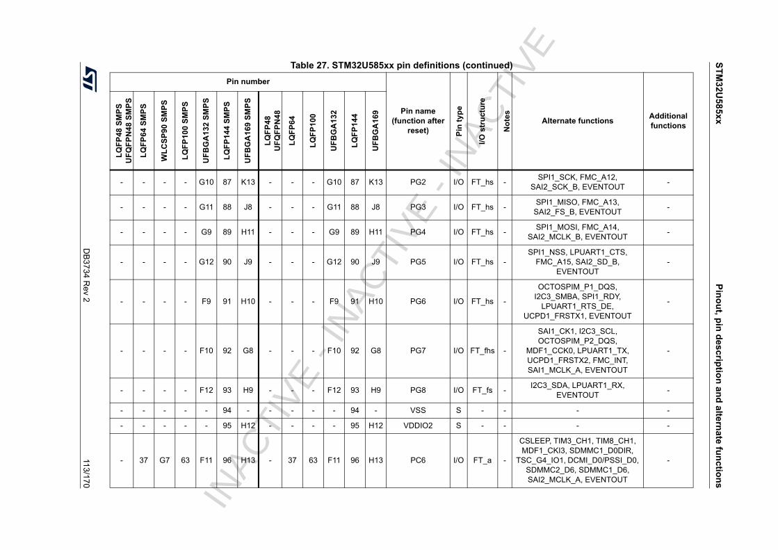
ST
M3
2U5
85x
xP
ino
ut, p
in d
escrip
tion
an
d a
ltern
ate
fun
ctio
ns
DB
3734 R
ev 2113/170
- - - - G10 87 K13 - - - G10 87 K13 PG2 I/O FT_hs -SPI1_SCK, FMC_A12,
SAI2_SCK_B, EVENTOUT-
- - - - G11 88 J8 - - - G11 88 J8 PG3 I/O FT_hs -SPI1_MISO, FMC_A13,
SAI2_FS_B, EVENTOUT-
- - - - G9 89 H11 - - - G9 89 H11 PG4 I/O FT_hs -SPI1_MOSI, FMC_A14,
SAI2_MCLK_B, EVENTOUT-
- - - - G12 90 J9 - - - G12 90 J9 PG5 I/O FT_hs -SPI1_NSS, LPUART1_CTS,
FMC_A15, SAI2_SD_B, EVENTOUT
-
- - - - F9 91 H10 - - - F9 91 H10 PG6 I/O FT_hs -
OCTOSPIM_P1_DQS, I2C3_SMBA, SPI1_RDY,
LPUART1_RTS_DE, UCPD1_FRSTX1, EVENTOUT
-
- - - - F10 92 G8 - - - F10 92 G8 PG7 I/O FT_fhs -
SAI1_CK1, I2C3_SCL, OCTOSPIM_P2_DQS,
MDF1_CCK0, LPUART1_TX, UCPD1_FRSTX2, FMC_INT, SAI1_MCLK_A, EVENTOUT
-
- - - - F12 93 H9 - - - F12 93 H9 PG8 I/O FT_fs -I2C3_SDA, LPUART1_RX,
EVENTOUT-
- - - - - 94 - - - - - 94 - VSS S - - - -
- - - - - 95 H12 - - - - 95 H12 VDDIO2 S - - - -
- 37 G7 63 F11 96 H13 - 37 63 F11 96 H13 PC6 I/O FT_a -
CSLEEP, TIM3_CH1, TIM8_CH1, MDF1_CKI3, SDMMC1_D0DIR,
TSC_G4_IO1, DCMI_D0/PSSI_D0, SDMMC2_D6, SDMMC1_D6, SAI2_MCLK_A, EVENTOUT
-
Table 27. STM32U585xx pin definitions (continued)
Pin number
Pin name (function after
reset) Pin
ty
pe
I/O s
tru
ctu
re
No
tes
Alternate functionsAdditional functions
LQ
FP
48 S
MP
SU
FQ
FP
N4
8 S
MP
S
LQ
FP
64 S
MP
S
WL
CS
P90
SM
PS
LQ
FP
10
0 S
MP
S
UF
BG
A1
32
SM
PS
LQ
FP
14
4 S
MP
S
UF
BG
A1
69
SM
PS
LQ
FP
48
UF
QF
PN
48
LQ
FP
64
LQ
FP
100
UF
BG
A13
2
LQ
FP
144
UF
BG
A16
9
INAC
TIVE
- IN
ACTI
VE -
INAC
TIVE

Pin
ou
t, pin
de
scrip
tion
an
d a
ltern
ate fun
ction
sS
TM
32U
585x
x
114/170
DB
3734 R
ev 2
- 38 F4 64 E10 97 G12 - 38 64 E10 97 G12 PC7 I/O FT_a -
CDSTOP, TIM3_CH2, TIM8_CH2, MDF1_SDI3, SDMMC1_D123DIR, TSC_G4_IO2, DCMI_D1/PSSI_D1,
SDMMC2_D7, SDMMC1_D7, SAI2_MCLK_B, LPTIM2_CH2,
EVENTOUT
-
- 39 F2 65 E12 98 G10 - 39 65 E12 98 G10 PC8 I/O FT_a -
SRDSTOP, TIM3_CH3, TIM8_CH3, TSC_G4_IO3, DCMI_D2/PSSI_D2,
SDMMC1_D0, LPTIM3_CH1, EVENTOUT
-
- 40 F6 66 E11 99 G9 - 40 66 E11 99 G9 PC9 I/O FT_a -
TRACED0, TIM8_BKIN2, TIM3_CH4, TIM8_CH4,
DCMI_D3/PSSI_D3, TSC_G4_IO4, OTG_FS_NOE, SDMMC1_D1,
LPTIM3_CH2, EVENTOUT
-
29 41 F8 67 D12 100 G7 29 41 67 D12 100 G7 PA8 I/O FT_hv -
MCO, TIM1_CH1, SAI1_CK2, SPI1_RDY, USART1_CK,
OTG_FS_SOF, TRACECLK, SAI1_SCK_A, LPTIM2_CH1,
EVENTOUT
-
30 42 E11 68 D10 101 G11 30 42 68 D10 101 G11 PA9 I/O FT_u -
TIM1_CH2, SPI2_SCK, DCMI_D0/PSSI_D0,
USART1_TX(boot), SAI1_FS_A, TIM15_BKIN, EVENTOUT
OTG_FS_VBUS
Table 27. STM32U585xx pin definitions (continued)
Pin number
Pin name (function after
reset) Pin
ty
pe
I/O s
tru
ctu
re
No
tes
Alternate functionsAdditional functions
LQ
FP
48 S
MP
SU
FQ
FP
N4
8 S
MP
S
LQ
FP
64 S
MP
S
WL
CS
P90
SM
PS
LQ
FP
10
0 S
MP
S
UF
BG
A1
32
SM
PS
LQ
FP
14
4 S
MP
S
UF
BG
A1
69
SM
PS
LQ
FP
48
UF
QF
PN
48
LQ
FP
64
LQ
FP
100
UF
BG
A13
2
LQ
FP
144
UF
BG
A16
9
INAC
TIVE
- IN
ACTI
VE -
INAC
TIVE

ST
M3
2U5
85x
xP
ino
ut, p
in d
escrip
tion
an
d a
ltern
ate
fun
ctio
ns
DB
3734 R
ev 2115/170
31 43 E1 69 D11 102 F11 31 43 69 D11 102 F11 PA10 I/O FT_u -
CRS_SYNC, TIM1_CH3, LPTIM2_IN2, SAI1_D1,
DCMI_D1/PSSI_D1, USART1_RX(boot), OTG_FS_ID,
SAI1_SD_A, TIM17_BKIN, EVENTOUT
-
32 44 E3 70 C12 103 G13 32 44 70 C12 103 G13 PA11 I/O FT_u -
TIM1_CH4, TIM1_BKIN2, SPI1_MISO, USART1_CTS,
FDCAN1_RX, OTG_FS_DM(boot), EVENTOUT
-
33 45 D2 71 B12 104 F13 33 45 71 B12 104 F13 PA12 I/O FT_u -
TIM1_ETR, SPI1_MOSI, OCTOSPIM_P2_NCS,
USART1_RTS_DE, FDCAN1_TX, OTG_FS_DP(boot), EVENTOUT
-
34 46 D4 72 C10 105 F12 34 46 72 C10 105 F12PA13 (JTMS/
SWDIO)I/O FT -
JTMS/SWDIO, IR_OUT, OTG_FS_NOE, SAI1_SD_B,
EVENTOUT-
- 47 - - - - - - 47 - - - - VSS S - - - -
- 48 C1 73 A12 106 E13 - 48 73 A12 106 E13 VDDUSB S - - - -
35 - B2 74 H4 107 E12 35 - 74 H4 107 E12 VSS S - - - -
36 - A1 75 D9 108 D13 36 - 75 D9 108 D13 VDD S - - - -
37 49 C3 76 C11 109 C10 37 49 76 C11 109 C10PA14 (JTCK/
SWCLK)I/O FT -
JTCK/SWCLK, LPTIM1_CH1, I2C1_SMBA, I2C4_SMBA,
OTG_FS_SOF, SAI1_FS_B, EVENTOUT
-
Table 27. STM32U585xx pin definitions (continued)
Pin number
Pin name (function after
reset) Pin
ty
pe
I/O s
tru
ctu
re
No
tes
Alternate functionsAdditional functions
LQ
FP
48 S
MP
SU
FQ
FP
N4
8 S
MP
S
LQ
FP
64 S
MP
S
WL
CS
P90
SM
PS
LQ
FP
10
0 S
MP
S
UF
BG
A1
32
SM
PS
LQ
FP
14
4 S
MP
S
UF
BG
A1
69
SM
PS
LQ
FP
48
UF
QF
PN
48
LQ
FP
64
LQ
FP
100
UF
BG
A13
2
LQ
FP
144
UF
BG
A16
9
INAC
TIVE
- IN
ACTI
VE -
INAC
TIVE

Pin
ou
t, pin
de
scrip
tion
an
d a
ltern
ate fun
ction
sS
TM
32U
585x
x
116/170
DB
3734 R
ev 2
38 50 E5 77 A11 110 A10 38 50 77 A11 110 A10 PA15 (JTDI) I/O FT_c -
JTDI, TIM2_CH1, TIM2_ETR, USART2_RX, SPI1_NSS,
SPI3_NSS, USART3_RTS_DE, UART4_RTS_DE, SAI2_FS_B,
EVENTOUT
UCPD1_CC1
- 51 E7 78 B11 111 C9 - 51 78 B11 111 C9 PC10 I/O FT_a -
TRACED1, LPTIM3_ETR, ADF1_CCK1, SPI3_SCK,
USART3_TX(boot), UART4_TX, TSC_G3_IO2, DCMI_D8/PSSI_D8,
LPGPIO1_P8, SDMMC1_D2, SAI2_SCK_B, EVENTOUT
-
- 52 A3 79 A10 112 A9 - 52 79 A10 112 A9 PC11 I/O FT_ha -
LPTIM3_IN1, ADF1_SDI0, DCMI_D2/PSSI_D2,
OCTOSPIM_P1_NCS, SPI3_MISO, USART3_RX(boot), UART4_RX,
TSC_G3_IO3, DCMI_D4/PSSI_D4, UCPD1_FRSTX2, SDMMC1_D3,
SAI2_MCLK_B, EVENTOUT
-
- 53 B4 80 B10 113 E8 - 53 80 B10 113 E8 PC12 I/OFT_hav
-
TRACED3, SPI3_MOSI, USART3_CK, UART5_TX,
TSC_G3_IO4, DCMI_D9/PSSI_D9, LPGPIO1_P10, SDMMC1_CK,
SAI2_SD_B, EVENTOUT
-
- - C5 81 C9 114 B9 - - 81 C9 114 B9 PD0 I/O FT_h -TIM8_CH4N, SPI2_NSS, FDCAN1_RX, FMC_D2,
EVENTOUT-
- - D6 82 B9 115 F6 - - 82 B9 115 F6 PD1 I/O FT_h -SPI2_SCK, FDCAN1_TX, FMC_D3,
EVENTOUT-
Table 27. STM32U585xx pin definitions (continued)
Pin number
Pin name (function after
reset) Pin
ty
pe
I/O s
tru
ctu
re
No
tes
Alternate functionsAdditional functions
LQ
FP
48 S
MP
SU
FQ
FP
N4
8 S
MP
S
LQ
FP
64 S
MP
S
WL
CS
P90
SM
PS
LQ
FP
10
0 S
MP
S
UF
BG
A1
32
SM
PS
LQ
FP
14
4 S
MP
S
UF
BG
A1
69
SM
PS
LQ
FP
48
UF
QF
PN
48
LQ
FP
64
LQ
FP
100
UF
BG
A13
2
LQ
FP
144
UF
BG
A16
9
INAC
TIVE
- IN
ACTI
VE -
INAC
TIVE

ST
M3
2U5
85x
xP
ino
ut, p
in d
escrip
tion
an
d a
ltern
ate
fun
ctio
ns
DB
3734 R
ev 2117/170
- 54 A5 83 A9 116 F7 - 54 83 A9 116 F7 PD2 I/O FT -
TRACED2, TIM3_ETR, USART3_RTS_DE, UART5_RX,
TSC_SYNC, DCMI_D11/PSSI_D11, LPGPIO1_P7, SDMMC1_CMD,
LPTIM4_ETR, EVENTOUT
-
- - - 84 C8 117 D8 - - 84 C8 117 D8 PD3 I/O FT_hv -
SPI2_SCK, DCMI_D5/PSSI_D5, SPI2_MISO, MDF1_SDI0,
USART2_CTS, OCTOSPIM_P2_NCS, FMC_CLK,
EVENTOUT
-
- - D8 85 B8 118 C8 - - 85 B8 118 C8 PD4 I/O FT_h -
SPI2_MOSI, MDF1_CKI0, USART2_RTS_DE,
OCTOSPIM_P1_IO4, FMC_NOE, EVENTOUT
-
- - B6 86 A8 119 E7 - - 86 A8 119 E7 PD5 I/O FT_h -SPI2_RDY, USART2_TX,
OCTOSPIM_P1_IO5, FMC_NWE, EVENTOUT
-
- - - - - 120 B8 - - - - 120 B8 VSS S - - - -
- - - - - 121 A8 - - - - 121 A8 VDD S - - - -
- - - 87 A7 122 B7 - - 87 A7 122 B7 PD6 I/O FT_hv -
SAI1_D1, DCMI_D10/PSSI_D10, SPI3_MOSI, MDF1_SDI1,
USART2_RX, OCTOSPIM_P1_IO6, SDMMC2_CK, FMC_NWAIT,
SAI1_SD_A, EVENTOUT
-
Table 27. STM32U585xx pin definitions (continued)
Pin number
Pin name (function after
reset) Pin
ty
pe
I/O s
tru
ctu
re
No
tes
Alternate functionsAdditional functions
LQ
FP
48 S
MP
SU
FQ
FP
N4
8 S
MP
S
LQ
FP
64 S
MP
S
WL
CS
P90
SM
PS
LQ
FP
10
0 S
MP
S
UF
BG
A1
32
SM
PS
LQ
FP
14
4 S
MP
S
UF
BG
A1
69
SM
PS
LQ
FP
48
UF
QF
PN
48
LQ
FP
64
LQ
FP
100
UF
BG
A13
2
LQ
FP
144
UF
BG
A16
9
INAC
TIVE
- IN
ACTI
VE -
INAC
TIVE

Pin
ou
t, pin
de
scrip
tion
an
d a
ltern
ate fun
ction
sS
TM
32U
585x
x
118/170
DB
3734 R
ev 2
- - - 88 D7 123 D7 - - 88 D7 123 D7 PD7 I/O FT_h -
MDF1_CKI1, USART2_CK, OCTOSPIM_P1_IO7,
SDMMC2_CMD, FMC_NCE/FMC_NE1,
LPTIM4_OUT, EVENTOUT
-
- - C7 - B7 124 A7 - - - B7 124 A7 PG9 I/O FT_hs -
OCTOSPIM_P2_IO6, SPI3_SCK(boot), USART1_TX,
FMC_NCE/FMC_NE2, SAI2_SCK_A, TIM15_CH1N,
EVENTOUT
-
- - A7 - C7 125 C7 - - - C7 125 C7 PG10 I/O FT_hs -
LPTIM1_IN1, OCTOSPIM_P2_IO7, SPI3_MISO(boot), USART1_RX,
FMC_NE3, SAI2_FS_A, TIM15_CH1, EVENTOUT
-
- - E9 - - - - - - - M11 126 M10 PG11 I/O FT_hs -
LPTIM1_IN2, OCTOSPIM_P1_IO5, SPI3_MOSI, USART1_CTS, SAI2_MCLK_A, TIM15_CH2,
EVENTOUT
-
- - B8 - A6 126 E6 - - - A6 127 E6 PG12 I/O FT_hs -
LPTIM1_ETR, OCTOSPIM_P2_NCS,
SPI3_NSS(boot), USART1_RTS_DE, FMC_NE4,
SAI2_SD_A, EVENTOUT
-
- - C9 - - 127 - - - - M10 128 N10 PG13 I/O FT_fhs -I2C1_SDA, SPI3_RDY,
USART1_CK, FMC_A24, EVENTOUT
-
- - A9 - - 128 - - - - M9 129 N9 PG14 I/O FT_fhs -LPTIM1_CH2, I2C1_SCL, FMC_A25, EVENTOUT
-
Table 27. STM32U585xx pin definitions (continued)
Pin number
Pin name (function after
reset) Pin
ty
pe
I/O s
tru
ctu
re
No
tes
Alternate functionsAdditional functions
LQ
FP
48 S
MP
SU
FQ
FP
N4
8 S
MP
S
LQ
FP
64 S
MP
S
WL
CS
P90
SM
PS
LQ
FP
10
0 S
MP
S
UF
BG
A1
32
SM
PS
LQ
FP
14
4 S
MP
S
UF
BG
A1
69
SM
PS
LQ
FP
48
UF
QF
PN
48
LQ
FP
64
LQ
FP
100
UF
BG
A13
2
LQ
FP
144
UF
BG
A16
9
INAC
TIVE
- IN
ACTI
VE -
INAC
TIVE

ST
M3
2U5
85x
xP
ino
ut, p
in d
escrip
tion
an
d a
ltern
ate
fun
ctio
ns
DB
3734 R
ev 2119/170
- - B10 - H9 129 - - - - H9 130 - VSS S - - - -
- - A11 - D8 130 A6 - - - D8 131 A6 VDDIO2 S - - - -
- - - - - 131 A5 - - - B4 132 A5 PG15 I/O FT_hs -LPTIM1_CH1, I2C1_SMBA,
OCTOSPIM_P2_DQS, DCMI_D13/PSSI_D13, EVENTOUT
-
39 55 D10 89 C6 132 D6 39 55 89 C6 133 D6PB3
(JTDO/TRACESWO)
I/O FT_fa -
JTDO/TRACESWO, TIM2_CH2, LPTIM1_CH1, ADF1_CCK0,
I2C1_SDA, SPI1_SCK, SPI3_SCK, USART1_RTS_DE, CRS_SYNC,
LPGPIO1_P11, SDMMC2_D2, SAI1_SCK_B, EVENTOUT
COMP2_INM2
40 56 C11 90 B6 133 B6 40 56 90 B6 134 B6 PB4 (NJTRST) I/O FT_fa -
NJTRST, LPTIM1_CH2, TIM3_CH1, ADF1_SDI0, I2C3_SDA, SPI1_MISO, SPI3_MISO,
USART1_CTS, UART5_RTS_DE, TSC_G2_IO1,
DCMI_D12/PSSI_D12, LPGPIO1_P12, SDMMC2_D3, SAI1_MCLK_B, TIM17_BKIN,
EVENTOUT
COMP2_INP1
41 57 D12 91 D6 134 C6 41 57 91 D6 135 C6 PB5 I/OFT_havd
-
LPTIM1_IN1, TIM3_CH2, OCTOSPIM_P1_NCLK,
I2C1_SMBA, SPI1_MOSI, SPI3_MOSI(boot), USART1_CK,
UART5_CTS, TSC_G2_IO2, DCMI_D10/PSSI_D10,
COMP2_OUT, SAI1_SD_B, TIM16_BKIN, EVENTOUT
UCPD1_DBCC1, WKUP6
Table 27. STM32U585xx pin definitions (continued)
Pin number
Pin name (function after
reset) Pin
ty
pe
I/O s
tru
ctu
re
No
tes
Alternate functionsAdditional functions
LQ
FP
48 S
MP
SU
FQ
FP
N4
8 S
MP
S
LQ
FP
64 S
MP
S
WL
CS
P90
SM
PS
LQ
FP
10
0 S
MP
S
UF
BG
A1
32
SM
PS
LQ
FP
14
4 S
MP
S
UF
BG
A1
69
SM
PS
LQ
FP
48
UF
QF
PN
48
LQ
FP
64
LQ
FP
100
UF
BG
A13
2
LQ
FP
144
UF
BG
A16
9
INAC
TIVE
- IN
ACTI
VE -
INAC
TIVE

Pin
ou
t, pin
de
scrip
tion
an
d a
ltern
ate fun
ction
sS
TM
32U
585x
x
120/170
DB
3734 R
ev 2
42 58 A13 92 A5 135 B5 42 58 92 A5 136 B5 PB6 I/O FT_fa -
LPTIM1_ETR, TIM4_CH1, TIM8_BKIN2, I2C1_SCL(boot),
I2C4_SCL, MDF1_SDI5, USART1_TX, TSC_G2_IO3,
DCMI_D5/PSSI_D5, SAI1_FS_B, TIM16_CH1N, EVENTOUT
COMP2_INP2,
WKUP3
43 59 B12 93 D5 136 F5 43 59 93 D5 137 F5 PB7 I/OFT_fhav
-
LPTIM1_IN2, TIM4_CH2, TIM8_BKIN, I2C1_SDA(boot),
I2C4_SDA, MDF1_CKI5, USART1_RX, UART4_CTS,
TSC_G2_IO4, DCMI_VSYNC/PSSI_RDY, FMC_NL, TIM17_CH1N,
EVENTOUT
COMP2_INM1,
PVD_IN, WKUP4
44 60 C13 94 B5 137 C5 44 60 94 B5 138 C5 PH3-BOOT0 I/O FT - EVENTOUT -
45 61 B14 95 C5 138 E5 45 61 95 C5 139 E5 PB8 I/O FT_f -
TIM4_CH3, SAI1_CK1, I2C1_SCL, MDF1_CCK0, SPI3_RDY,
SDMMC1_CKIN, FDCAN1_RX(boot),
DCMI_D6/PSSI_D6, SDMMC2_D4, SDMMC1_D4, SAI1_MCLK_A,
TIM16_CH1, EVENTOUT
WKUP5
- - A15 96 A4 139 D5 46 62 96 A4 140 D5 PB9 I/O FT_f -
IR_OUT, TIM4_CH4, SAI1_D2, I2C1_SDA, SPI2_NSS,
SDMMC1_CDIR, FDCAN1_TX(boot),
DCMI_D7/PSSI_D7, SDMMC2_D5, SDMMC1_D5, SAI1_FS_A, TIM17_CH1, EVENTOUT
-
Table 27. STM32U585xx pin definitions (continued)
Pin number
Pin name (function after
reset) Pin
ty
pe
I/O s
tru
ctu
re
No
tes
Alternate functionsAdditional functions
LQ
FP
48 S
MP
SU
FQ
FP
N4
8 S
MP
S
LQ
FP
64 S
MP
S
WL
CS
P90
SM
PS
LQ
FP
10
0 S
MP
S
UF
BG
A1
32
SM
PS
LQ
FP
14
4 S
MP
S
UF
BG
A1
69
SM
PS
LQ
FP
48
UF
QF
PN
48
LQ
FP
64
LQ
FP
100
UF
BG
A13
2
LQ
FP
144
UF
BG
A16
9
INAC
TIVE
- IN
ACTI
VE -
INAC
TIVE

ST
M3
2U5
85x
xP
ino
ut, p
in d
escrip
tion
an
d a
ltern
ate
fun
ctio
ns
DB
3734 R
ev 21
21/170
- - - 97 C4 140 D4 - - 97 C4 141 D4 PE0 I/O FT_h -TIM4_ETR, DCMI_D2/PSSI_D2,
LPGPIO1_P13, FMC_NBL0, TIM16_CH1, EVENTOUT
-
- - - - A3 141 C4 - - 98 A3 142 C4 PE1 I/O FT_h -DCMI_D3/PSSI_D3, FMC_NBL1,
TIM17_CH1, EVENTOUT-
- - - - - - - - - - - - A4 VCAP S - - - -
46 62 A17 98 B4 142 A4 - - - - - - VDD11 S - - - -
47 63 B16 99 E4 143 B4 47 63 99 E4 143 B4 VSS S - - - -
48 64 B18 100 J9 144 A3 48 64 100 J9 144 A3 VDD S - - - -
- - - - - - B11 - - - - - B11 VSS S - - - -
- - - - - - F10 - - - - - F10 PH2 I/O FT_h - OCTOSPIM_P1_IO4, EVENTOUT -
- - - - - - E10 - - - - - E10 PH4 I/O FT_fh -I2C2_SCL, OCTOSPIM_P2_DQS,
PSSI_D14, EVENTOUT-
- - - - - - F9 - - - - - F9 PH5 I/O FT_f -I2C2_SDA,
DCMI_PIXCLK/PSSI_PDCK, EVENTOUT
-
- - - - - - E11 - - - - - E11 PH6 I/O FT_hv -I2C2_SMBA, OCTOSPIM_P2_CLK,
DCMI_D8/PSSI_D8, EVENTOUT-
- - - - - - F8 - - - - - F8 PH7 I/OFT_fhv
-I2C3_SCL, OCTOSPIM_P2_NCLK, DCMI_D9/PSSI_D9, EVENTOUT
-
- - - - - - D12 - - - - - D12 PH8 I/O FT_fh -I2C3_SDA, OCTOSPIM_P2_IO3,
DCMI_HSYNC/PSSI_DE, EVENTOUT
-
Table 27. STM32U585xx pin definitions (continued)
Pin number
Pin name (function after
reset) Pin
ty
pe
I/O s
tru
ctu
re
No
tes
Alternate functionsAdditional functions
LQ
FP
48 S
MP
SU
FQ
FP
N4
8 S
MP
S
LQ
FP
64 S
MP
S
WL
CS
P90
SM
PS
LQ
FP
10
0 S
MP
S
UF
BG
A1
32
SM
PS
LQ
FP
14
4 S
MP
S
UF
BG
A1
69
SM
PS
LQ
FP
48
UF
QF
PN
48
LQ
FP
64
LQ
FP
100
UF
BG
A13
2
LQ
FP
144
UF
BG
A16
9
INAC
TIVE
- IN
ACTI
VE -
INAC
TIVE

Pin
ou
t, pin
de
scrip
tion
an
d a
ltern
ate fun
ction
sS
TM
32U
585x
x
122/170
DB
3734 R
ev 2
- - - - - - E9 - - - - - E9 PH9 I/O FT_h -I2C3_SMBA, OCTOSPIM_P2_IO4, DCMI_D0/PSSI_D0, EVENTOUT
-
- - - - - - C13 - - - - - C13 PH10 I/O FT_h -TIM5_CH1, OCTOSPIM_P2_IO5, DCMI_D1/PSSI_D1, EVENTOUT
-
- - - - - - D9 - - - - - D9 PH11 I/O FT_h -TIM5_CH2, OCTOSPIM_P2_IO6, DCMI_D2/PSSI_D2, EVENTOUT
-
- - - - - - B13 - - - - - B13 PH12 I/O FT_h -TIM5_CH3, TIM8_CH4N,
OCTOSPIM_P2_IO7, DCMI_D3/PSSI_D3, EVENTOUT
-
- - - - - - C12 - - - - - C12 PH13 I/O FT -TIM8_CH1N, FDCAN1_TX,
EVENTOUT-
- - - - - - C11 - - - - - C11 PH14 I/O FT -TIM8_CH2N, FDCAN1_RX,
DCMI_D4/PSSI_D4, EVENTOUT-
- - - - - - A13 - - - - - A13 PH15 I/O FT_h -TIM8_CH3N, OCTOSPIM_P2_IO6, DCMI_D11/PSSI_D11, EVENTOUT
-
- - - - - - A11 - - - - - A11 VDD S - - - -
- - - - - - B12 - - - - - B12 PI0 I/O FT_h -TIM5_CH4, OCTOSPIM_P1_IO5,
SPI2_NSS, DCMI_D13/PSSI_D13, EVENTOUT
-
- - - - - - A12 - - - - - A12 PI1 I/O FT_h -SPI2_SCK, OCTOSPIM_P2_IO2, DCMI_D8/PSSI_D8, EVENTOUT
-
- - - - - - D11 - - - - - D11 PI2 I/O FT_hv -TIM8_CH4, SPI2_MISO,
OCTOSPIM_P2_IO1, DCMI_D9/PSSI_D9, EVENTOUT
-
Table 27. STM32U585xx pin definitions (continued)
Pin number
Pin name (function after
reset) Pin
ty
pe
I/O s
tru
ctu
re
No
tes
Alternate functionsAdditional functions
LQ
FP
48 S
MP
SU
FQ
FP
N4
8 S
MP
S
LQ
FP
64 S
MP
S
WL
CS
P90
SM
PS
LQ
FP
10
0 S
MP
S
UF
BG
A1
32
SM
PS
LQ
FP
14
4 S
MP
S
UF
BG
A1
69
SM
PS
LQ
FP
48
UF
QF
PN
48
LQ
FP
64
LQ
FP
100
UF
BG
A13
2
LQ
FP
144
UF
BG
A16
9
INAC
TIVE
- IN
ACTI
VE -
INAC
TIVE

ST
M3
2U5
85x
xP
ino
ut, p
in d
escrip
tion
an
d a
ltern
ate
fun
ctio
ns
DB
3734 R
ev 21
23/170
- - - - - - D10 - - - - - D10 PI3 I/O FT_h -TIM8_ETR, SPI2_MOSI,
OCTOSPIM_P2_IO0, DCMI_D10/PSSI_D10, EVENTOUT
-
- - - - - - B2 - - - - - B2 VSS S - - - -
- - - - - - B1 - - - - - B1 VDD S - - - -
- - - - - - B10 - - - - - B10 PI4 I/O FT -TIM8_BKIN, SPI2_RDY,
DCMI_D5/PSSI_D5, EVENTOUT-
- - - - - - B3 - - - - - B3 PI5 I/O FT_h -TIM8_CH1, OCTOSPIM_P2_NCS,
DCMI_VSYNC/PSSI_RDY, EVENTOUT
-
- - - - - - A2 - - - - - A2 PI6 I/O FT_hv -TIM8_CH2, OCTOSPIM_P2_CLK, DCMI_D6/PSSI_D6, EVENTOUT
-
- - - - - - C3 - - - - - C3 PI7 I/O FT_hv -TIM8_CH3, OCTOSPIM_P2_NCLK,
DCMI_D7/PSSI_D7, EVENTOUT-
Table 27. STM32U585xx pin definitions (continued)
Pin number
Pin name (function after
reset) Pin
ty
pe
I/O s
tru
ctu
re
No
tes
Alternate functionsAdditional functions
LQ
FP
48 S
MP
SU
FQ
FP
N4
8 S
MP
S
LQ
FP
64 S
MP
S
WL
CS
P90
SM
PS
LQ
FP
10
0 S
MP
S
UF
BG
A1
32
SM
PS
LQ
FP
14
4 S
MP
S
UF
BG
A1
69
SM
PS
LQ
FP
48
UF
QF
PN
48
LQ
FP
64
LQ
FP
100
UF
BG
A13
2
LQ
FP
144
UF
BG
A16
9
INAC
TIVE
- IN
ACTI
VE -
INAC
TIVE

Pin
ou
t, pin
de
scrip
tion
an
d a
ltern
ate fun
ction
sS
TM
32U
585x
x
124/170
DB
3734 R
ev 2
4.3 Alternate functions
Table 28. Alternate function AF0 to AF7(1)
Port
AF0 AF1 AF2 AF3 AF4 AF5 AF6 AF7
CRS/LPTIM1/SYS_AF
LPTIM1/TIM1/2/5/8
LPTIM1/2/3/TIM1/2/3/4/5
ADF1/I2C4/OCTOSPIM_P1/OTG_FS/SAI1/SPI2/TIM1/8/
USART2
DCMI/I2C1/2/3/4/
LPTIM3
DCMI/I2C4/MDF1/OCTOSPIM_P1/2/
SPI1/2/3
I2C3/MDF1/OCTOSPIM_P2/
SPI3USART1/2/3
Por
t A
PA0 - TIM2_CH1 TIM5_CH1 TIM8_ETR - - SPI3_RDY USART2_CTS
PA1 LPTIM1_CH2 TIM2_CH2 TIM5_CH2 - I2C1_SMBA SPI1_SCK -USART2_RTS_DE
PA2 - TIM2_CH3 TIM5_CH3 - - SPI1_RDY - USART2_TX
PA3 - TIM2_CH4 TIM5_CH4 SAI1_CK1 - - - USART2_RX
PA4 - - -OCTOSPIM_P1
_NCS- SPI1_NSS SPI3_NSS USART2_CK
PA5 CSLEEP TIM2_CH1 TIM2_ETR TIM8_CH1N PSSI_D14 SPI1_SCK - USART3_RX
PA6 CDSTOP TIM1_BKIN TIM3_CH1 TIM8_BKINDCMI_PIXCL
K/PSSI_PDCK
SPI1_MISO - USART3_CTS
PA7 SRDSTOP TIM1_CH1N TIM3_CH2 TIM8_CH1N I2C3_SCL SPI1_MOSI - USART3_TX
PA8 MCO TIM1_CH1 - SAI1_CK2 - SPI1_RDY - USART1_CK
PA9 - TIM1_CH2 - SPI2_SCK - DCMI_D0/PSSI_D0 - USART1_TX
PA10 CRS_SYNC TIM1_CH3 LPTIM2_IN2 SAI1_D1 - DCMI_D1/PSSI_D1 - USART1_RX
PA11 - TIM1_CH4 TIM1_BKIN2 - - SPI1_MISO - USART1_CTS
PA12 - TIM1_ETR - - - SPI1_MOSIOCTOSPIM_
P2_NCSUSART1_RTS_DE
PA13 JTMS/SWDIO IR_OUT - - - - - -
PA14 JTCK/SWCLK LPTIM1_CH1 - - I2C1_SMBA I2C4_SMBA - -
PA15 JTDI TIM2_CH1 TIM2_ETR USART2_RX - SPI1_NSS SPI3_NSSUSART3_RTS_DE
INAC
TIVE
- IN
ACTI
VE -
INAC
TIVE

ST
M3
2U5
85x
xP
ino
ut, p
in d
escrip
tion
an
d a
ltern
ate
fun
ctio
ns
DB
3734 R
ev 21
25/170
Por
t B
PB0 - TIM1_CH2N TIM3_CH3 TIM8_CH2N LPTIM3_CH1 SPI1_NSS - USART3_CK
PB1 - TIM1_CH3N TIM3_CH4 TIM8_CH3N LPTIM3_CH2 - MDF1_SDI0USART3_RTS_DE
PB2 - LPTIM1_CH1 - TIM8_CH4N I2C3_SMBA SPI1_RDY MDF1_CKI0 -
PB3JTDO/
TRACESWOTIM2_CH2 LPTIM1_CH1 ADF1_CCK0 I2C1_SDA SPI1_SCK SPI3_SCK
USART1_RTS_DE
PB4 NJTRST LPTIM1_CH2 TIM3_CH1 ADF1_SDI0 I2C3_SDA SPI1_MISO SPI3_MISO USART1_CTS
PB5 - LPTIM1_IN1 TIM3_CH2OCTOSPIM_
P1_NCLKI2C1_SMBA SPI1_MOSI SPI3_MOSI USART1_CK
PB6 - LPTIM1_ETR TIM4_CH1 TIM8_BKIN2 I2C1_SCL I2C4_SCL MDF1_SDI5 USART1_TX
PB7 - LPTIM1_IN2 TIM4_CH2 TIM8_BKIN I2C1_SDA I2C4_SDA MDF1_CKI5 USART1_RX
PB8 - - TIM4_CH3 SAI1_CK1 I2C1_SCL MDF1_CCK0 SPI3_RDY -
PB9 - IR_OUT TIM4_CH4 SAI1_D2 I2C1_SDA SPI2_NSS - -
PB10 - TIM2_CH3 LPTIM3_CH1 I2C4_SCL I2C2_SCL SPI2_SCK - USART3_TX
PB11 - TIM2_CH4 - I2C4_SDA I2C2_SDA SPI2_RDY - USART3_RX
PB12 - TIM1_BKIN - - I2C2_SMBA SPI2_NSS MDF1_SDI1 USART3_CK
PB13 - TIM1_CH1N LPTIM3_IN1 - I2C2_SCL SPI2_SCK MDF1_CKI1 USART3_CTS
PB14 - TIM1_CH2N LPTIM3_ETR TIM8_CH2N I2C2_SDA SPI2_MISO MDF1_SDI2USART3_RTS_DE
PB15 RTC_REFIN TIM1_CH3N LPTIM2_IN2 TIM8_CH3N - SPI2_MOSI MDF1_CKI2 -
Table 28. Alternate function AF0 to AF7(1) (continued)
Port
AF0 AF1 AF2 AF3 AF4 AF5 AF6 AF7
CRS/LPTIM1/SYS_AF
LPTIM1/TIM1/2/5/8
LPTIM1/2/3/TIM1/2/3/4/5
ADF1/I2C4/OCTOSPIM_P1/OTG_FS/SAI1/SPI2/TIM1/8/
USART2
DCMI/I2C1/2/3/4/
LPTIM3
DCMI/I2C4/MDF1/OCTOSPIM_P1/2/
SPI1/2/3
I2C3/MDF1/OCTOSPIM_P2/
SPI3USART1/2/3
INAC
TIVE
- IN
ACTI
VE -
INAC
TIVE

Pin
ou
t, pin
de
scrip
tion
an
d a
ltern
ate fun
ction
sS
TM
32U
585x
x
126/170
DB
3734 R
ev 2
Por
t C
PC0 - LPTIM1_IN1 -OCTOSPIM_
P1_IO7I2C3_SCL SPI2_RDY MDF1_SDI4 -
PC1 TRACED0 LPTIM1_CH1 - SPI2_MOSI I2C3_SDA - MDF1_CKI4 -
PC2 - LPTIM1_IN2 - - - SPI2_MISO MDF1_CCK1 -
PC3 - LPTIM1_ETR LPTIM3_CH1 SAI1_D1 - SPI2_MOSI - -
PC4 - - - - - - - USART3_TX
PC5 - TIM1_CH4N - SAI1_D3 PSSI_D15 - - USART3_RX
PC6 CSLEEP - TIM3_CH1 TIM8_CH1 - - MDF1_CKI3 -
PC7 CDSTOP - TIM3_CH2 TIM8_CH2 - - MDF1_SDI3 -
PC8 SRDSTOP - TIM3_CH3 TIM8_CH3 - - - -
PC9 TRACED0 TIM8_BKIN2 TIM3_CH4 TIM8_CH4DCMI_D3/PSSI_D3
- - -
PC10 TRACED1 - LPTIM3_ETR ADF1_CCK1 - - SPI3_SCK USART3_TX
PC11 - - LPTIM3_IN1 ADF1_SDI0DCMI_D2/PSSI_D2
OCTOSPIM_P1_NCS
SPI3_MISO USART3_RX
PC12 TRACED3 - - - - - SPI3_MOSI USART3_CK
PC13 - - - - - - - -
PC14 - - - - - - - -
PC15 - - - - - - - -
Table 28. Alternate function AF0 to AF7(1) (continued)
Port
AF0 AF1 AF2 AF3 AF4 AF5 AF6 AF7
CRS/LPTIM1/SYS_AF
LPTIM1/TIM1/2/5/8
LPTIM1/2/3/TIM1/2/3/4/5
ADF1/I2C4/OCTOSPIM_P1/OTG_FS/SAI1/SPI2/TIM1/8/
USART2
DCMI/I2C1/2/3/4/
LPTIM3
DCMI/I2C4/MDF1/OCTOSPIM_P1/2/
SPI1/2/3
I2C3/MDF1/OCTOSPIM_P2/
SPI3USART1/2/3
INAC
TIVE
- IN
ACTI
VE -
INAC
TIVE

ST
M3
2U5
85x
xP
ino
ut, p
in d
escrip
tion
an
d a
ltern
ate
fun
ctio
ns
DB
3734 R
ev 21
27/170
Por
t D
PD0 - - - TIM8_CH4N - SPI2_NSS - -
PD1 - - - - - SPI2_SCK - -
PD2 TRACED2 - TIM3_ETR - - - -USART3_RTS_DE
PD3 - - - SPI2_SCKDCMI_D5/PSSI_D5
SPI2_MISO MDF1_SDI0 USART2_CTS
PD4 - - - - - SPI2_MOSI MDF1_CKI0USART2_RTS_DE
PD5 - - - - - SPI2_RDY - USART2_TX
PD6 - - - SAI1_D1DCMI_D10/PSSI_D10
SPI3_MOSI MDF1_SDI1 USART2_RX
PD7 - - - - - - MDF1_CKI1 USART2_CK
PD8 - - - - - - - USART3_TX
PD9 - - LPTIM2_IN2 - - - - USART3_RX
PD10 - - LPTIM2_CH2 - - - - USART3_CK
PD11 - - - - I2C4_SMBA - - USART3_CTS
PD12 - - TIM4_CH1 - I2C4_SCL - -USART3_RTS_DE
PD13 - - TIM4_CH2 - I2C4_SDA - - -
PD14 - - TIM4_CH3 - - - - -
PD15 - - TIM4_CH4 - - - - -
Table 28. Alternate function AF0 to AF7(1) (continued)
Port
AF0 AF1 AF2 AF3 AF4 AF5 AF6 AF7
CRS/LPTIM1/SYS_AF
LPTIM1/TIM1/2/5/8
LPTIM1/2/3/TIM1/2/3/4/5
ADF1/I2C4/OCTOSPIM_P1/OTG_FS/SAI1/SPI2/TIM1/8/
USART2
DCMI/I2C1/2/3/4/
LPTIM3
DCMI/I2C4/MDF1/OCTOSPIM_P1/2/
SPI1/2/3
I2C3/MDF1/OCTOSPIM_P2/
SPI3USART1/2/3
INAC
TIVE
- IN
ACTI
VE -
INAC
TIVE

Pin
ou
t, pin
de
scrip
tion
an
d a
ltern
ate fun
ction
sS
TM
32U
585x
x
128/170
DB
3734 R
ev 2
Por
t E
PE0 - - TIM4_ETR - - - - -
PE1 - - - - - - - -
PE2 TRACECLK - TIM3_ETR SAI1_CK1 - - - -
PE3 TRACED0 - TIM3_CH1OCTOSPIM_
P1_DQS- - - -
PE4 TRACED1 - TIM3_CH2 SAI1_D2 - - MDF1_SDI3 -
PE5 TRACED2 - TIM3_CH3 SAI1_CK2 - - MDF1_CKI3 -
PE6 TRACED3 - TIM3_CH4 SAI1_D1 - - - -
PE7 - TIM1_ETR - - - - MDF1_SDI2 -
PE8 - TIM1_CH1N - - - - MDF1_CKI2 -
PE9 - TIM1_CH1 - ADF1_CCK0 - - MDF1_CCK0 -
PE10 - TIM1_CH2N - ADF1_SDI0 - - MDF1_SDI4 -
PE11 - TIM1_CH2 - - - SPI1_RDY MDF1_CKI4 -
PE12 - TIM1_CH3N - - - SPI1_NSS MDF1_SDI5 -
PE13 - TIM1_CH3 - - - SPI1_SCK MDF1_CKI5 -
PE14 - TIM1_CH4 TIM1_BKIN2 - - SPI1_MISO - -
PE15 - TIM1_BKIN - TIM1_CH4N - SPI1_MOSI - -
Table 28. Alternate function AF0 to AF7(1) (continued)
Port
AF0 AF1 AF2 AF3 AF4 AF5 AF6 AF7
CRS/LPTIM1/SYS_AF
LPTIM1/TIM1/2/5/8
LPTIM1/2/3/TIM1/2/3/4/5
ADF1/I2C4/OCTOSPIM_P1/OTG_FS/SAI1/SPI2/TIM1/8/
USART2
DCMI/I2C1/2/3/4/
LPTIM3
DCMI/I2C4/MDF1/OCTOSPIM_P1/2/
SPI1/2/3
I2C3/MDF1/OCTOSPIM_P2/
SPI3USART1/2/3
INAC
TIVE
- IN
ACTI
VE -
INAC
TIVE

ST
M3
2U5
85x
xP
ino
ut, p
in d
escrip
tion
an
d a
ltern
ate
fun
ctio
ns
DB
3734 R
ev 21
29/170
Por
t F
PF0 - - - - I2C2_SDA OCTOSPIM_P2_IO0 - -
PF1 - - - - I2C2_SCL OCTOSPIM_P2_IO1 - -
PF2 - - LPTIM3_CH2 - I2C2_SMBA OCTOSPIM_P2_IO2 - -
PF3 - - LPTIM3_IN1 - - OCTOSPIM_P2_IO3 - -
PF4 - - LPTIM3_ETR - -OCTOSPIM_
P2_CLK- -
PF5 - - LPTIM3_CH1 - -OCTOSPIM_
P2_NCLK- -
PF6 - TIM5_ETR TIM5_CH1 -DCMI_D12/P
SSI_D12OCTOSPIM_
P2_NCS- -
PF7 - - TIM5_CH2 - - - - -
PF8 - - TIM5_CH3 - PSSI_D14 - - -
PF9 - - TIM5_CH4 - PSSI_D15 - - -
PF10 - - -OCTOSPIM_
P1_CLKPSSI_D15 - MDF1_CCK1 -
PF11 - - -OCTOSPIM_
P1_NCLK- - - -
PF12 - - - - -OCTOSPIM_
P2_DQS- -
PF13 - - - - I2C4_SMBA - - -
PF14 - - - - I2C4_SCL - - -
PF15 - - - - I2C4_SDA - - -
Table 28. Alternate function AF0 to AF7(1) (continued)
Port
AF0 AF1 AF2 AF3 AF4 AF5 AF6 AF7
CRS/LPTIM1/SYS_AF
LPTIM1/TIM1/2/5/8
LPTIM1/2/3/TIM1/2/3/4/5
ADF1/I2C4/OCTOSPIM_P1/OTG_FS/SAI1/SPI2/TIM1/8/
USART2
DCMI/I2C1/2/3/4/
LPTIM3
DCMI/I2C4/MDF1/OCTOSPIM_P1/2/
SPI1/2/3
I2C3/MDF1/OCTOSPIM_P2/
SPI3USART1/2/3
INAC
TIVE
- IN
ACTI
VE -
INAC
TIVE

Pin
ou
t, pin
de
scrip
tion
an
d a
ltern
ate fun
ction
sS
TM
32U
585x
x
130/170
DB
3734 R
ev 2
Por
t G
PG0 - - - - - OCTOSPIM_P2_IO4 - -
PG1 - - - - - OCTOSPIM_P2_IO5 - -
PG2 - - - - - SPI1_SCK - -
PG3 - - - - - SPI1_MISO - -
PG4 - - - - - SPI1_MOSI - -
PG5 - - - - - SPI1_NSS - -
PG6 - - -OCTOSPIM_
P1_DQSI2C3_SMBA SPI1_RDY - -
PG7 - - - SAI1_CK1 I2C3_SCLOCTOSPIM_
P2_DQSMDF1_CCK0 -
PG8 - - - - I2C3_SDA - - -
PG9 - - - - - OCTOSPIM_P2_IO6 SPI3_SCK USART1_TX
PG10 - LPTIM1_IN1 - - - OCTOSPIM_P2_IO7 SPI3_MISO USART1_RX
PG11 - LPTIM1_IN2 -OCTOSPIM_
P1_IO5- - SPI3_MOSI USART1_CTS
PG12 - LPTIM1_ETR - - -OCTOSPIM_
P2_NCSSPI3_NSS
USART1_RTS_DE
PG13 - - - - I2C1_SDA - SPI3_RDY USART1_CK
PG14 - LPTIM1_CH2 - - I2C1_SCL - - -
PG15 - LPTIM1_CH1 - - I2C1_SMBAOCTOSPIM_
P2_DQS- -
Table 28. Alternate function AF0 to AF7(1) (continued)
Port
AF0 AF1 AF2 AF3 AF4 AF5 AF6 AF7
CRS/LPTIM1/SYS_AF
LPTIM1/TIM1/2/5/8
LPTIM1/2/3/TIM1/2/3/4/5
ADF1/I2C4/OCTOSPIM_P1/OTG_FS/SAI1/SPI2/TIM1/8/
USART2
DCMI/I2C1/2/3/4/
LPTIM3
DCMI/I2C4/MDF1/OCTOSPIM_P1/2/
SPI1/2/3
I2C3/MDF1/OCTOSPIM_P2/
SPI3USART1/2/3
INAC
TIVE
- IN
ACTI
VE -
INAC
TIVE

ST
M3
2U5
85x
xP
ino
ut, p
in d
escrip
tion
an
d a
ltern
ate
fun
ctio
ns
DB
3734 R
ev 21
31/170
Por
t H
PH0 - - - - - - - -
PH1 - - - - - - - -
PH2 - - -OCTOSPIM_
P1_IO4- - - -
PH3 - - - - - - - -
PH4 - - - - I2C2_SCLOCTOSPIM_
P2_DQS- -
PH5 - - - - I2C2_SDA - - -
PH6 - - - - I2C2_SMBAOCTOSPIM_
P2_CLK- -
PH7 - - - - I2C3_SCLOCTOSPIM_
P2_NCLK- -
PH8 - - - - I2C3_SDA OCTOSPIM_P2_IO3 - -
PH9 - - - - I2C3_SMBA OCTOSPIM_P2_IO4 - -
PH10 - - TIM5_CH1 - - OCTOSPIM_P2_IO5 - -
PH11 - - TIM5_CH2 - - OCTOSPIM_P2_IO6 - -
PH12 - - TIM5_CH3 TIM8_CH4N - OCTOSPIM_P2_IO7 - -
PH13 - - - TIM8_CH1N - - - -
PH14 - - - TIM8_CH2N - - - -
PH15 - - - TIM8_CH3N - OCTOSPIM_P2_IO6 - -
Table 28. Alternate function AF0 to AF7(1) (continued)
Port
AF0 AF1 AF2 AF3 AF4 AF5 AF6 AF7
CRS/LPTIM1/SYS_AF
LPTIM1/TIM1/2/5/8
LPTIM1/2/3/TIM1/2/3/4/5
ADF1/I2C4/OCTOSPIM_P1/OTG_FS/SAI1/SPI2/TIM1/8/
USART2
DCMI/I2C1/2/3/4/
LPTIM3
DCMI/I2C4/MDF1/OCTOSPIM_P1/2/
SPI1/2/3
I2C3/MDF1/OCTOSPIM_P2/
SPI3USART1/2/3
INAC
TIVE
- IN
ACTI
VE -
INAC
TIVE
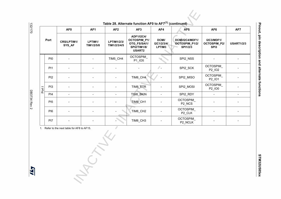
Pin
ou
t, pin
de
scrip
tion
an
d a
ltern
ate fun
ction
sS
TM
32U
585x
x
132/170
DB
3734 R
ev 2
Por
t I
PI0 - - TIM5_CH4OCTOSPIM_
P1_IO5- SPI2_NSS - -
PI1 - - - - - SPI2_SCKOCTOSPIM_
P2_IO2-
PI2 - - - TIM8_CH4 - SPI2_MISOOCTOSPIM_
P2_IO1-
PI3 - - - TIM8_ETR - SPI2_MOSIOCTOSPIM_
P2_IO0-
PI4 - - - TIM8_BKIN - SPI2_RDY - -
PI5 - - - TIM8_CH1 -OCTOSPIM_
P2_NCS- -
PI6 - - - TIM8_CH2 -OCTOSPIM_
P2_CLK- -
PI7 - - - TIM8_CH3 -OCTOSPIM_
P2_NCLK- -
1. Refer to the next table for AF8 to AF15.
Table 28. Alternate function AF0 to AF7(1) (continued)
Port
AF0 AF1 AF2 AF3 AF4 AF5 AF6 AF7
CRS/LPTIM1/SYS_AF
LPTIM1/TIM1/2/5/8
LPTIM1/2/3/TIM1/2/3/4/5
ADF1/I2C4/OCTOSPIM_P1/OTG_FS/SAI1/SPI2/TIM1/8/
USART2
DCMI/I2C1/2/3/4/
LPTIM3
DCMI/I2C4/MDF1/OCTOSPIM_P1/2/
SPI1/2/3
I2C3/MDF1/OCTOSPIM_P2/
SPI3USART1/2/3
INAC
TIVE
- IN
ACTI
VE -
INAC
TIVE

ST
M3
2U5
85x
xP
ino
ut, p
in d
escrip
tion
an
d a
ltern
ate
fun
ctio
ns
DB
3734 R
ev 21
33/170
Table 29. Alternate function AF8 to AF15(1)
Port
AF8 AF9 AF10 AF11 AF12 AF13 AF14 AF15
LPUART1/SDMMC1/UART4/5
CAN1/TSCCRS/DCMI/
OCTOSPIM_P1/2/OTG_FS
LPGPIO/SDMMC2/UCPD1
COMP1/2/FMC/SDMMC1/2
LPTIM2/4/SAI1/2
LPTIM2/3/TIM2/15/16/17
EVENOUTP
ort A
PA0 UART4_TX -OCTOSPIM_
P2_NCS- SDMMC2_CMD AUDIOCLK TIM2_ETR EVENTOUT
PA1 UART4_RX -OCTOSPIM_
P1_DQSLPGPIO1_P0 - - TIM15_CH1N EVENTOUT
PA2 LPUART1_TX -OCTOSPIM_
P1_NCSUCPD1_FRSTX1
- - TIM15_CH1 EVENTOUT
PA3 LPUART1_RX - OCTOSPIM_P1_CLK LPGPIO1_P1 - SAI1_MCLK_A TIM15_CH2 EVENTOUT
PA4 - -DCMI_HSYNC/
PSSI_DE- - SAI1_FS_B LPTIM2_CH1 EVENTOUT
PA5 - - - - - - LPTIM2_ETR EVENTOUT
PA6 LPUART1_CTS - OCTOSPIM_P1_IO3 LPGPIO1_P2 - - TIM16_CH1 EVENTOUT
PA7 - - OCTOSPIM_P1_IO2 - - LPTIM2_CH2 TIM17_CH1 EVENTOUT
PA8 - - OTG_FS_SOF - TRACECLK SAI1_SCK_A LPTIM2_CH1 EVENTOUT
PA9 - - - - - SAI1_FS_A TIM15_BKIN EVENTOUT
PA10 - - OTG_FS_ID - - SAI1_SD_A TIM17_BKIN EVENTOUT
PA11 - FDCAN1_RX OTG_FS_DM - - - - EVENTOUT
PA12 - FDCAN1_TX OTG_FS_DP - - - - EVENTOUT
PA13 - - OTG_FS_NOE - - SAI1_SD_B - EVENTOUT
PA14 - - OTG_FS_SOF - - SAI1_FS_B - EVENTOUT
PA15 UART4_RTS_DE - - - - SAI2_FS_B - EVENTOUT
INAC
TIVE
- IN
ACTI
VE -
INAC
TIVE

Pin
ou
t, pin
de
scrip
tion
an
d a
ltern
ate fun
ction
sS
TM
32U
585x
x
134/170
DB
3734 R
ev 2
Por
t B
PB0 - - OCTOSPIM_P1_IO1 LPGPIO1_P9 COMP1_OUT AUDIOCLK - EVENTOUT
PB1LPUART1_RTS_DE
- OCTOSPIM_P1_IO0 LPGPIO1_P3 - - LPTIM2_IN1 EVENTOUT
PB2 - -OCTOSPIM_
P1_DQSUCPD1_FRSTX1
- - - EVENTOUT
PB3 - - CRS_SYNC LPGPIO1_P11 SDMMC2_D2 SAI1_SCK_B - EVENTOUT
PB4 UART5_RTS_DE TSC_G2_IO1DCMI_D12/PSSI_D12
LPGPIO1_P12 SDMMC2_D3 SAI1_MCLK_B TIM17_BKIN EVENTOUT
PB5 UART5_CTS TSC_G2_IO2DCMI_D10/PSSI_D10
- COMP2_OUT SAI1_SD_B TIM16_BKIN EVENTOUT
PB6 - TSC_G2_IO3 DCMI_D5/PSSI_D5 - - SAI1_FS_B TIM16_CH1N EVENTOUT
PB7 UART4_CTS TSC_G2_IO4DCMI_VSYNC/
PSSI_RDY- FMC_NL - TIM17_CH1N EVENTOUT
PB8 SDMMC1_CKIN FDCAN1_RX DCMI_D6/PSSI_D6 SDMMC2_D4 SDMMC1_D4 SAI1_MCLK_A TIM16_CH1 EVENTOUT
PB9 SDMMC1_CDIR FDCAN1_TX DCMI_D7/PSSI_D7 SDMMC2_D5 SDMMC1_D5 SAI1_FS_A TIM17_CH1 EVENTOUT
PB10 LPUART1_RX TSC_SYNC OCTOSPIM_P1_CLK LPGPIO1_P4 COMP1_OUT SAI1_SCK_A - EVENTOUT
PB11 LPUART1_TX -OCTOSPIM_
P1_NCS- COMP2_OUT - - EVENTOUT
PB12LPUART1_RTS_
DETSC_G1_IO1
OCTOSPIM_P1_NCLK
- - SAI2_FS_A TIM15_BKIN EVENTOUT
PB13 LPUART1_CTS TSC_G1_IO2 - - - SAI2_SCK_A TIM15_CH1N EVENTOUT
PB14 - TSC_G1_IO3 - - SDMMC2_D0 SAI2_MCLK_A TIM15_CH1 EVENTOUT
PB15 - - - FMC_NBL1 SDMMC2_D1 SAI2_SD_A TIM15_CH2 EVENTOUT
Table 29. Alternate function AF8 to AF15(1) (continued)
Port
AF8 AF9 AF10 AF11 AF12 AF13 AF14 AF15
LPUART1/SDMMC1/UART4/5
CAN1/TSCCRS/DCMI/
OCTOSPIM_P1/2/OTG_FS
LPGPIO/SDMMC2/UCPD1
COMP1/2/FMC/SDMMC1/2
LPTIM2/4/SAI1/2
LPTIM2/3/TIM2/15/16/17
EVENOUT
INAC
TIVE
- IN
ACTI
VE -
INAC
TIVE

ST
M3
2U5
85x
xP
ino
ut, p
in d
escrip
tion
an
d a
ltern
ate
fun
ctio
ns
DB
3734 R
ev 21
35/170
Por
t C
PC0 LPUART1_RX - - - SDMMC1_D5 SAI2_FS_A LPTIM2_IN1 EVENTOUT
PC1 LPUART1_TX - OCTOSPIM_P1_IO4 - SDMMC2_CK SAI1_SD_A - EVENTOUT
PC2 - TSC_G3_IO1 OCTOSPIM_P1_IO5 LPGPIO1_P5 - - - EVENTOUT
PC3 - TSC_G1_IO4 OCTOSPIM_P1_IO6 - - SAI1_SD_A LPTIM2_ETR EVENTOUT
PC4 - - OCTOSPIM_P1_IO7 - - - - EVENTOUT
PC5 - - - - - - - EVENTOUT
PC6SDMMC1_
D0DIRTSC_G4_IO1 DCMI_D0/PSSI_D0 SDMMC2_D6 SDMMC1_D6 SAI2_MCLK_A - EVENTOUT
PC7SDMMC1_D123DIR
TSC_G4_IO2 DCMI_D1/PSSI_D1 SDMMC2_D7 SDMMC1_D7 SAI2_MCLK_B LPTIM2_CH2 EVENTOUT
PC8 - TSC_G4_IO3 DCMI_D2/PSSI_D2 - SDMMC1_D0 - LPTIM3_CH1 EVENTOUT
PC9 - TSC_G4_IO4 OTG_FS_NOE - SDMMC1_D1 - LPTIM3_CH2 EVENTOUT
PC10 UART4_TX TSC_G3_IO2 DCMI_D8/PSSI_D8 LPGPIO1_P8 SDMMC1_D2 SAI2_SCK_B - EVENTOUT
PC11 UART4_RX TSC_G3_IO3 DCMI_D4/PSSI_D4UCPD1_FRSTX2
SDMMC1_D3 SAI2_MCLK_B - EVENTOUT
PC12 UART5_TX TSC_G3_IO4 DCMI_D9/PSSI_D9 LPGPIO1_P10 SDMMC1_CK SAI2_SD_B - EVENTOUT
PC13 - - - - - - - EVENTOUT
PC14 - - - - - - - EVENTOUT
PC15 - - - - - - - EVENTOUT
Table 29. Alternate function AF8 to AF15(1) (continued)
Port
AF8 AF9 AF10 AF11 AF12 AF13 AF14 AF15
LPUART1/SDMMC1/UART4/5
CAN1/TSCCRS/DCMI/
OCTOSPIM_P1/2/OTG_FS
LPGPIO/SDMMC2/UCPD1
COMP1/2/FMC/SDMMC1/2
LPTIM2/4/SAI1/2
LPTIM2/3/TIM2/15/16/17
EVENOUT
INAC
TIVE
- IN
ACTI
VE -
INAC
TIVE

Pin
ou
t, pin
de
scrip
tion
an
d a
ltern
ate fun
ction
sS
TM
32U
585x
x
136/170
DB
3734 R
ev 2 Por
t D
PD0 - FDCAN1_RX - - FMC_D2 - - EVENTOUT
PD1 - FDCAN1_TX - - FMC_D3 - - EVENTOUT
PD2 UART5_RX TSC_SYNCDCMI_D11/PSSI_D11
LPGPIO1_P7 SDMMC1_CMD LPTIM4_ETR - EVENTOUT
PD3 - -OCTOSPIM_
P2_NCS- FMC_CLK - - EVENTOUT
PD4 - - OCTOSPIM_P1_IO4 - FMC_NOE - - EVENTOUT
PD5 - - OCTOSPIM_P1_IO5 - FMC_NWE - - EVENTOUT
PD6 - - OCTOSPIM_P1_IO6 SDMMC2_CK FMC_NWAIT SAI1_SD_A - EVENTOUT
PD7 - - OCTOSPIM_P1_IO7 SDMMC2_CMDFMC_NCE/FMC_NE1
LPTIM4_OUT - EVENTOUT
PD8 - -DCMI_HSYNC/
PSSI_DE- FMC_D13 - - EVENTOUT
PD9 - -DCMI_PIXCLK/
PSSI_PDCK- FMC_D14 SAI2_MCLK_A LPTIM3_IN1 EVENTOUT
PD10 - TSC_G6_IO1 - - FMC_D15 SAI2_SCK_A LPTIM3_ETR EVENTOUT
PD11 - TSC_G6_IO2 - - FMC_A16 SAI2_SD_A LPTIM2_ETR EVENTOUT
PD12 - TSC_G6_IO3 - - FMC_A17 SAI2_FS_A LPTIM2_IN1 EVENTOUT
PD13 - TSC_G6_IO4 - LPGPIO1_P6 FMC_A18 LPTIM4_IN1 LPTIM2_CH1 EVENTOUT
PD14 - - - - FMC_D0 - LPTIM3_CH1 EVENTOUT
PD15 - - - - FMC_D1 - LPTIM3_CH2 EVENTOUT
Table 29. Alternate function AF8 to AF15(1) (continued)
Port
AF8 AF9 AF10 AF11 AF12 AF13 AF14 AF15
LPUART1/SDMMC1/UART4/5
CAN1/TSCCRS/DCMI/
OCTOSPIM_P1/2/OTG_FS
LPGPIO/SDMMC2/UCPD1
COMP1/2/FMC/SDMMC1/2
LPTIM2/4/SAI1/2
LPTIM2/3/TIM2/15/16/17
EVENOUT
INAC
TIVE
- IN
ACTI
VE -
INAC
TIVE

ST
M3
2U5
85x
xP
ino
ut, p
in d
escrip
tion
an
d a
ltern
ate
fun
ctio
ns
DB
3734 R
ev 21
37/170
Por
t E
PE0 - - DCMI_D2/PSSI_D2 LPGPIO1_P13 FMC_NBL0 - TIM16_CH1 EVENTOUT
PE1 - - DCMI_D3/PSSI_D3 - FMC_NBL1 - TIM17_CH1 EVENTOUT
PE2 - TSC_G7_IO1 - LPGPIO1_P14 FMC_A23 SAI1_MCLK_A - EVENTOUT
PE3 - TSC_G7_IO2 - LPGPIO1_P15 FMC_A19 SAI1_SD_B - EVENTOUT
PE4 - TSC_G7_IO3 DCMI_D4/PSSI_D4 - FMC_A20 SAI1_FS_A - EVENTOUT
PE5 - TSC_G7_IO4 DCMI_D6/PSSI_D6 - FMC_A21 SAI1_SCK_A - EVENTOUT
PE6 - - DCMI_D7/PSSI_D7 - FMC_A22 SAI1_SD_A - EVENTOUT
PE7 - - - - FMC_D4 SAI1_SD_B - EVENTOUT
PE8 - - - - FMC_D5 SAI1_SCK_B - EVENTOUT
PE9 - -OCTOSPIM_P1_NC
LK- FMC_D6 SAI1_FS_B - EVENTOUT
PE10 - TSC_G5_IO1 OCTOSPIM_P1_CLK - FMC_D7 SAI1_MCLK_B - EVENTOUT
PE11 - TSC_G5_IO2OCTOSPIM_
P1_NCS- FMC_D8 - - EVENTOUT
PE12 - TSC_G5_IO3 OCTOSPIM_P1_IO0 - FMC_D9 - - EVENTOUT
PE13 - TSC_G5_IO4 OCTOSPIM_P1_IO1 - FMC_D10 - - EVENTOUT
PE14 - - OCTOSPIM_P1_IO2 - FMC_D11 - - EVENTOUT
PE15 - - OCTOSPIM_P1_IO3 - FMC_D12 - - EVENTOUT
Table 29. Alternate function AF8 to AF15(1) (continued)
Port
AF8 AF9 AF10 AF11 AF12 AF13 AF14 AF15
LPUART1/SDMMC1/UART4/5
CAN1/TSCCRS/DCMI/
OCTOSPIM_P1/2/OTG_FS
LPGPIO/SDMMC2/UCPD1
COMP1/2/FMC/SDMMC1/2
LPTIM2/4/SAI1/2
LPTIM2/3/TIM2/15/16/17
EVENOUT
INAC
TIVE
- IN
ACTI
VE -
INAC
TIVE

Pin
ou
t, pin
de
scrip
tion
an
d a
ltern
ate fun
ction
sS
TM
32U
585x
x
138/170
DB
3734 R
ev 2
Por
t F
PF0 - - - - FMC_A0 - - EVENTOUT
PF1 - - - - FMC_A1 - - EVENTOUT
PF2 - - - - FMC_A2 - - EVENTOUT
PF3 - - - - FMC_A3 - - EVENTOUT
PF4 - - - - FMC_A4 - - EVENTOUT
PF5 - - - - FMC_A5 - - EVENTOUT
PF6 - - OCTOSPIM_P1_IO3 - - SAI1_SD_B - EVENTOUT
PF7 - FDCAN1_RX OCTOSPIM_P1_IO2 - - SAI1_MCLK_B - EVENTOUT
PF8 - FDCAN1_TX OCTOSPIM_P1_IO0 - - SAI1_SCK_B - EVENTOUT
PF9 - - OCTOSPIM_P1_IO1 - - SAI1_FS_B TIM15_CH1 EVENTOUT
PF10 - -DCMI_D11/PSSI_D11
- - SAI1_D3 TIM15_CH2 EVENTOUT
PF11 - -DCMI_D12/PSSI_D12
- - LPTIM4_IN1 - EVENTOUT
PF12 - - - - FMC_A6 LPTIM4_ETR - EVENTOUT
PF13 - - -UCPD1_FRSTX2
FMC_A7 LPTIM4_OUT - EVENTOUT
PF14 - TSC_G8_IO1 - - FMC_A8 - - EVENTOUT
PF15 - TSC_G8_IO2 - - FMC_A9 - - EVENTOUT
Table 29. Alternate function AF8 to AF15(1) (continued)
Port
AF8 AF9 AF10 AF11 AF12 AF13 AF14 AF15
LPUART1/SDMMC1/UART4/5
CAN1/TSCCRS/DCMI/
OCTOSPIM_P1/2/OTG_FS
LPGPIO/SDMMC2/UCPD1
COMP1/2/FMC/SDMMC1/2
LPTIM2/4/SAI1/2
LPTIM2/3/TIM2/15/16/17
EVENOUT
INAC
TIVE
- IN
ACTI
VE -
INAC
TIVE

ST
M3
2U5
85x
xP
ino
ut, p
in d
escrip
tion
an
d a
ltern
ate
fun
ctio
ns
DB
3734 R
ev 21
39/170
Por
t G
PG0 - TSC_G8_IO3 - - FMC_A10 - - EVENTOUT
PG1 - TSC_G8_IO4 - - FMC_A11 - - EVENTOUT
PG2 - - - - FMC_A12 SAI2_SCK_B - EVENTOUT
PG3 - - - - FMC_A13 SAI2_FS_B - EVENTOUT
PG4 - - - - FMC_A14 SAI2_MCLK_B - EVENTOUT
PG5 LPUART1_CTS - - - FMC_A15 SAI2_SD_B - EVENTOUT
PG6LPUART1_RTS_DE
- -UCPD1_FRSTX1
- - - EVENTOUT
PG7 LPUART1_TX - -UCPD1_FRSTX2
FMC_INT SAI1_MCLK_A - EVENTOUT
PG8 LPUART1_RX - - - - - - EVENTOUT
PG9 - - - -FMC_NCE/FMC_NE2
SAI2_SCK_A TIM15_CH1N EVENTOUT
PG10 - - - - FMC_NE3 SAI2_FS_A TIM15_CH1 EVENTOUT
PG11 - - - - - SAI2_MCLK_A TIM15_CH2 EVENTOUT
PG12 - - - - FMC_NE4 SAI2_SD_A - EVENTOUT
PG13 - - - - FMC_A24 - - EVENTOUT
PG14 - - - - FMC_A25 - - EVENTOUT
PG15 - -DCMI_D13/PSSI_D13
- - - - EVENTOUT
Table 29. Alternate function AF8 to AF15(1) (continued)
Port
AF8 AF9 AF10 AF11 AF12 AF13 AF14 AF15
LPUART1/SDMMC1/UART4/5
CAN1/TSCCRS/DCMI/
OCTOSPIM_P1/2/OTG_FS
LPGPIO/SDMMC2/UCPD1
COMP1/2/FMC/SDMMC1/2
LPTIM2/4/SAI1/2
LPTIM2/3/TIM2/15/16/17
EVENOUT
INAC
TIVE
- IN
ACTI
VE -
INAC
TIVE

Pin
ou
t, pin
de
scrip
tion
an
d a
ltern
ate fun
ction
sS
TM
32U
585x
x
140/170
DB
3734 R
ev 2
Por
t H
PH0 - - - - - - - EVENTOUT
PH1 - - - - - - - EVENTOUT
PH2 - - - - - - - EVENTOUT
PH3 - - - - - - - EVENTOUT
PH4 - - PSSI_D14 - - - - EVENTOUT
PH5 - -DCMI_PIXCLK/
PSSI_PDCK- - - - EVENTOUT
PH6 - - DCMI_D8/PSSI_D8 - - - - EVENTOUT
PH7 - - DCMI_D9/PSSI_D9 - - - - EVENTOUT
PH8 - -DCMI_HSYNC/
PSSI_DE- - - - EVENTOUT
PH9 - - DCMI_D0/PSSI_D0 - - - - EVENTOUT
PH10 - - DCMI_D1/PSSI_D1 - - - - EVENTOUT
PH11 - - DCMI_D2/PSSI_D2 - - - - EVENTOUT
PH12 - - DCMI_D3/PSSI_D3 - - - - EVENTOUT
PH13 - FDCAN1_TX - - - - - EVENTOUT
PH14 - FDCAN1_RX DCMI_D4/PSSI_D4 - - - - EVENTOUT
PH15 - -DCMI_D11/PSSI_D11
- - - - EVENTOUT
Table 29. Alternate function AF8 to AF15(1) (continued)
Port
AF8 AF9 AF10 AF11 AF12 AF13 AF14 AF15
LPUART1/SDMMC1/UART4/5
CAN1/TSCCRS/DCMI/
OCTOSPIM_P1/2/OTG_FS
LPGPIO/SDMMC2/UCPD1
COMP1/2/FMC/SDMMC1/2
LPTIM2/4/SAI1/2
LPTIM2/3/TIM2/15/16/17
EVENOUT
INAC
TIVE
- IN
ACTI
VE -
INAC
TIVE

ST
M3
2U5
85x
xP
ino
ut, p
in d
escrip
tion
an
d a
ltern
ate
fun
ctio
ns
DB
3734 R
ev 21
41/170
Por
t I
PI0 - -DCMI_D13/PSSI_D13
- - - - EVENTOUT
PI1 - - DCMI_D8/PSSI_D8 - - - - EVENTOUT
PI2 - - DCMI_D9/PSSI_D9 - - - - EVENTOUT
PI3 - -DCMI_D10/PSSI_D10
- - - - EVENTOUT
PI4 - - DCMI_D5/PSSI_D5 - - - - EVENTOUT
PI5 - -DCMI_VSYNC/
PSSI_RDY- - - - EVENTOUT
PI6 - - DCMI_D6/PSSI_D6 - - - - EVENTOUT
PI7 - - DCMI_D7/PSSI_D7 - - - - EVENTOUT
1. For AF0 to AF7 refer to the previous table.
Table 29. Alternate function AF8 to AF15(1) (continued)
Port
AF8 AF9 AF10 AF11 AF12 AF13 AF14 AF15
LPUART1/SDMMC1/UART4/5
CAN1/TSCCRS/DCMI/
OCTOSPIM_P1/2/OTG_FS
LPGPIO/SDMMC2/UCPD1
COMP1/2/FMC/SDMMC1/2
LPTIM2/4/SAI1/2
LPTIM2/3/TIM2/15/16/17
EVENOUT
INAC
TIVE
- IN
ACTI
VE -
INAC
TIVE

Package information STM32U585xx
142/170 DB3734 Rev 2
5 Package information
In order to meet environmental requirements, ST offers these devices in different grades of ECOPACK packages, depending on their level of environmental compliance. ECOPACK specifications, grade definitions and product status are available at: www.st.com. ECOPACK is an ST trademark.
5.1 UFQFPN48 package information
This UFQFPN is a 48 leads, 7x7 mm, 0.5 mm pitch, ultra thin fine pitch quad flat package
Figure 22. UFQFPN48 - Outline
1. Drawing is not to scale.
2. All leads/pads should also be soldered to the PCB to improve the lead/pad solder joint life.
3. There is an exposed die pad on the underside of the UFQFPN package. It is recommended to connect and solder this back-side pad to PCB ground.
A0B9_ME_V3
D
Pin 1 identifierlaser marking area
E E
DY
D2
E2
Exposed pad area
Z
1
48
Detail Z
R 0.125 typ.
1
48L
C 0.500x45°pin1 corner
A
Seating planeA1
beddd
Detail Y
T
INAC
TIVE
- IN
ACTI
VE -
INAC
TIVE

DB3734 Rev 2 143/170
STM32U585xx Package information
167
Figure 23. UFQFPN48 - Recommended footprint
1. Dimensions are expressed in millimeters.
Table 30. UFQFPN48 - Mechanical data
Symbolmillimeters inches(1)
1. Values in inches are converted from mm and rounded to 4 decimal digits.
Min Typ Max Min Typ Max
A 0.500 0.550 0.600 0.0197 0.0217 0.0236
A1 0.000 0.020 0.050 0.0000 0.0008 0.0020
D 6.900 7.000 7.100 0.2717 0.2756 0.2795
E 6.900 7.000 7.100 0.2717 0.2756 0.2795
D2 5.500 5.600 5.700 0.2165 0.2205 0.2244
E2 5.500 5.600 5.700 0.2165 0.2205 0.2244
L 0.300 0.400 0.500 0.0118 0.0157 0.0197
T - 0.152 - - 0.0060 -
b 0.200 0.250 0.300 0.0079 0.0098 0.0118
e - 0.500 - - 0.0197 -
ddd - - 0.080 - - 0.0031
7.30
7.30
0.20
0.30
0.550.50
5.80
6.20
6.20
5.60
5.60
5.80
0.75
A0B9_FP_V2
48
1
12
13 24
25
36
37
INAC
TIVE
- IN
ACTI
VE -
INAC
TIVE

Package information STM32U585xx
144/170 DB3734 Rev 2
Device marking for UFQFPN48
The following figure gives an example of topside marking versus pin 1 position identifier location.
The printed markings may differ depending on the supply chain.
Other optional marking or inset/upset marks, which depend on supply chain operations, are not indicated below.
Figure 24. UFQFPN48 marking example (package top view)
1. Parts marked as “ES”, “E” or accompanied by an Engineering Sample notification letter, are not yet qualified and therefore not approved for use in production. ST is not responsible for any consequences resulting from such use. In no event will ST be liable for the customer using any of these engineering samples in production. ST’s Quality department must be contacted prior to any decision to use these engineering samples to run a qualification activity.
MSv64351V2
Date code
Pin 1 identifier
CIU6
Product identification(1)
R
Y WW
STM32U585
Revision code
INAC
TIVE
- IN
ACTI
VE -
INAC
TIVE

DB3734 Rev 2 145/170
STM32U585xx Package information
167
5.2 LQFP48 package information
This LQFP is a 48-pin, 7 x 7 mm low-profile quad flat package
Figure 25. LQFP48 - Outline
1. Drawing is not to scale.
Table 31. LQFP48 - Mechanical data
Symbolmillimeters inches(1)
Min Typ Max Min Typ Max
A - - 1.600 - - 0.0630
A1 0.050 - 0.150 0.0020 - 0.0059
A2 1.350 1.400 1.450 0.0531 0.0551 0.0571
b 0.170 0.220 0.270 0.0067 0.0087 0.0106
c 0.090 - 0.200 0.0035 - 0.0079
D 8.800 9.000 9.200 0.3465 0.3543 0.3622
D1 6.800 7.000 7.200 0.2677 0.2756 0.2835
D3 - 5.500 - - 0.2165 -
E 8.800 9.000 9.200 0.3465 0.3543 0.3622
5B_ME_V2
PIN 1IDENTIFICATION
ccc C
C
D3
0.25 mmGAUGE PLANE
b
A1
A A2
cA
1
L1LD
D1
E3 E1 E
e
121
13
24
2536
37
48
SEATINGPLANE
K
INAC
TIVE
- IN
ACTI
VE -
INAC
TIVE

Package information STM32U585xx
146/170 DB3734 Rev 2
Figure 26. LQFP48 - Recommended footprint
1. Dimensions are expressed in millimeters.
E1 6.800 7.000 7.200 0.2677 0.2756 0.2835
E3 - 5.500 - - 0.2165 -
e - 0.500 - - 0.0197 -
L 0.450 0.600 0.750 0.0177 0.0236 0.0295
L1 - 1.000 - - 0.0394 -
k 0° 3.5° 7° 0° 3.5° 7°
ccc - - 0.080 - - 0.0031
1. Values in inches are converted from mm and rounded to 4 decimal digits.
Table 31. LQFP48 - Mechanical data (continued)
Symbolmillimeters inches(1)
Min Typ Max Min Typ Max
9.70 5.80 7.30
12
24
0.20
7.30
1
3736
1.20
5.80
9.70
0.3025
1.20
0.50
ai14911d
1348
INAC
TIVE
- IN
ACTI
VE -
INAC
TIVE
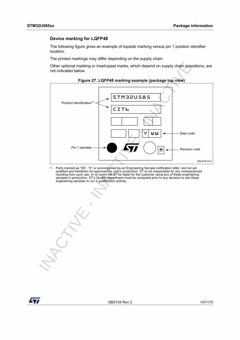
DB3734 Rev 2 147/170
STM32U585xx Package information
167
Device marking for LQFP48
The following figure gives an example of topside marking versus pin 1 position identifier location.
The printed markings may differ depending on the supply chain.
Other optional marking or inset/upset marks, which depend on supply chain operations, are not indicated below.
Figure 27. LQFP48 marking example (package top view)
1. Parts marked as “ES”, “E” or accompanied by an Engineering Sample notification letter, are not yet qualified and therefore not approved for use in production. ST is not responsible for any consequences resulting from such use. In no event will ST be liable for the customer using any of these engineering samples in production. ST’s Quality department must be contacted prior to any decision to use these engineering samples to run a qualification activity.
MSv67814V1
Date code
Pin 1 identifier
CIT6
Product identification(1)
R
Y WW
STM32U585
Revision code
INAC
TIVE
- IN
ACTI
VE -
INAC
TIVE

Package information STM32U585xx
148/170 DB3734 Rev 2
5.3 LQFP64 package information
This LQFP is 64-pin, 10 x 10 mm low-profile quad flat package.
Figure 28. LQFP64 - Outline
1. Drawing is not to scale.
Table 32. LQFP64 - Mechanical data
Symbolmillimeters inches(1)
Min Typ Max Min Typ Max
A - - 1.600 - - 0.0630
A1 0.050 - 0.150 0.0020 - 0.0059
A2 1.350 1.400 1.450 0.0531 0.0551 0.0571
b 0.170 0.220 0.270 0.0067 0.0087 0.0106
c 0.090 - 0.200 0.0035 - 0.0079
D - 12.000 - - 0.4724 -
D1 - 10.000 - - 0.3937 -
D3 - 7.500 - - 0.2953 -
E - 12.000 - - 0.4724 -
E1 - 10.000 - - 0.3937 -
5W_ME_V3
A1
A2A
SEATING PLANE
ccc C
b
C
c
A1
LL1
K
IDENTIFICATIONPIN 1
DD1D3
e1 16
17
32
3348
49
64
E3 E1 E
GAUGE PLANE0.25 mm
INAC
TIVE
- IN
ACTI
VE -
INAC
TIVE

DB3734 Rev 2 149/170
STM32U585xx Package information
167
Figure 29. LQFP64 - Recommended footprint
1. Dimensions are expressed in millimeters.
E3 - 7.500 - - 0.2953 -
e - 0.500 - - 0.0197 -
K 0° 3.5° 7° 0° 3.5° 7°
L 0.450 0.600 0.750 0.0177 0.0236 0.0295
L1 - 1.000 - - 0.0394 -
ccc - - 0.080 - - 0.0031
1. Values in inches are converted from mm and rounded to 4 decimal digits.
Table 32. LQFP64 - Mechanical data (continued)
Symbolmillimeters inches(1)
Min Typ Max Min Typ Max
48
3249
64 17
1 16
1.2
0.3
33
10.3
12.7
10.3
0.5
7.8
12.7
ai14909c
INAC
TIVE
- IN
ACTI
VE -
INAC
TIVE

Package information STM32U585xx
150/170 DB3734 Rev 2
Device marking for LQFP64
The following figure gives an example of topside marking orientation versus pin 1 identifier location.
The printed markings may differ depending on the supply chain.
Other optional marking or inset/upset marks, which also depend on supply chain operations, are not indicated below.
Figure 30. LQFP64 marking example (package top view)
1. Parts marked as ES or E or accompanied by an Engineering Sample notification letter are not yet qualified and therefore not approved for use in production. ST is not responsible for any consequences resulting from such use. In no event will ST be liable for the customer using any of these engineering samples in production. ST’s Quality department must be contacted prior to any decision to use these engineering samples to run a qualification activity.
MSv64352V1
Date code
Pin 1 identifier
RIT6
Product identification(1)
Revision codeR
Y WW
STM32U585
INAC
TIVE
- IN
ACTI
VE -
INAC
TIVE

DB3734 Rev 2 151/170
STM32U585xx Package information
167
5.4 WLSCP90 package information
WLCSP is a 90 balls, 4.20 x 3.95 mm, 0.4 mm pitch, wafer level chip scale package.
Figure 31. WLCSP90 - Outline
1. Drawing is not to scale.
2. Dimension is measured at the maximum bump diameter parallel to primary datum Z.
3. Primary datum Z and seating plane are defined by the spherical crowns of the bump.
4. Bump position designation per JESD 95-1, SPP-010.
Table 33. WLCSP90 - Mechanical data
Symbolmillimeters inches(1)
Min Typ Max Min Typ Max
A(2) - - 0.59 - - 0.023
A1 - 0.18 - - 0.007 -
A2 - 0.38 - - 0.015 -
A3(3) - 0.025 - - 0.001 -
b 0.22 0.25 0.28 0.009 0.010 0.011
D 4.19 4.20 4.21 0.165 0.165 0.166
E 3.93 3.95 3.97 0.155 0.156 0.156
Z
B01C_WLCSP90_ME_V2
Z
BOTTOM VIEW TOP VIEW SIDE VIEW
FRONT VIEW
DETAIL AROTATED 90
SEATING PLANE
D
ee
e2 E
FG
e1
A1 BALL LOCATION
A1
B2B4
aaa(4x)
bbb ZA1
A2A
A3 A2
b
BUMP
eeeA1
b (90x)cccddd
Z X YZ
DETAIL A
INAC
TIVE
- IN
ACTI
VE -
INAC
TIVE

Package information STM32U585xx
152/170 DB3734 Rev 2
Figure 32. WLCSP90 - Recommended footprint
e - 0.40 - - 0.016 -
e1 - 3.40 - - 0.134 -
e2 - 3.12 - - 0.123 -
F(4) - 0.400 - - 0.016 -
G(4) - 0.416 - - 0.016 -
aaa - - 0.10 - - 0.004
bbb - - 0.10 - - 0.004
ccc - - 0.10 - - 0.004
ddd - - 0.05 - - 0.002
eee - - 0.05 - - 0.002
1. Values in inches are converted from mm and rounded to 4 decimal digits.
2. The maximum total package height is calculated by the RSS method (Root Sum Square) using nominal and tolerances values of A1 and A2.
3. Back side coating. Nominal dimension is rounded to the 3rd decimal place resulting from process capability.
4. Calculated dimensions are rounded to the 3rd decimal place
Table 34. WLCSP90 - Recommended PCB design rules
Dimension Recommended values
Pitch 0.4 mm
Dpad 0,225 mm
Dsm 0.290 mm typ. (depends on soldermask registration tolerance)
Stencil opening 0.250 mm
Stencil thickness 0.100 mm
Table 33. WLCSP90 - Mechanical data (continued)
Symbolmillimeters inches(1)
Min Typ Max Min Typ Max
B03P_WLCSP36_DIE464_FP_V1
Dpad
Dsm
INAC
TIVE
- IN
ACTI
VE -
INAC
TIVE

DB3734 Rev 2 153/170
STM32U585xx Package information
167
Device marking for WLCSP90
The following figure gives an example of topside marking orientation versus pin 1 identifier location.
The printed markings may differ depending on the supply chain.
Other optional marking or inset/upset marks, which also depend on supply chain operations, are not indicated below.
Figure 33. WLCSP90 marking example (package top view)
1. Parts marked as ES or E or accompanied by an Engineering Sample notification letter are not yet qualified and therefore not approved for use in production. ST is not responsible for any consequences resulting from such use. In no event will ST be liable for the customer using any of these engineering samples in production. ST’s Quality department must be contacted prior to any decision to use these engineering samples to run a qualification activity.
MSv67815V1
Pin 1 identifier
Product identification(1)
RY WW
U585OI6Q
Revision codeDate code
INAC
TIVE
- IN
ACTI
VE -
INAC
TIVE

Package information STM32U585xx
154/170 DB3734 Rev 2
5.5 LQFP100 package information
This LQFP is100 pins, 14 x 14 mm low-profile quad flat package.
Figure 34. LQFP100 - Outline
1. Drawing is not to scale.
Table 35. LQPF100 - Mechanical data
Symbolmillimeters inches(1)
Min Typ Max Min Typ Max
A - - 1.600 - - 0.0630
A1 0.050 - 0.150 0.0020 - 0.0059
A2 1.350 1.400 1.450 0.0531 0.0551 0.0571
b 0.170 0.220 0.270 0.0067 0.0087 0.0106
c 0.090 - 0.200 0.0035 - 0.0079
D 15.800 16.000 16.200 0.6220 0.6299 0.6378
D1 13.800 14.000 14.200 0.5433 0.5512 0.5591
D3 - 12.000 - - 0.4724 -
E 15.800 16.000 16.200 0.6220 0.6299 0.6378
eIDENTIFICATIONPIN 1
GAUGE PLANE0.25 mm
SEATING PLANE
DD1D3
E3 E1 E
K
ccc C
C
1 25
26100
76
75 51
50
1L_ME_V5
A2A A1
L1L
c
b
A1
INAC
TIVE
- IN
ACTI
VE -
INAC
TIVE

DB3734 Rev 2 155/170
STM32U585xx Package information
167
Figure 35. LQFP100 - Recommended footprint
1. Dimensions are expressed in millimeters.
E1 13.800 14.000 14.200 0.5433 0.5512 0.5591
E3 - 12.000 - - 0.4724 -
e - 0.500 - - 0.0197 -
L 0.450 0.600 0.750 0.0177 0.0236 0.0295
L1 - 1.000 - - 0.0394 -
k 0.0° 3.5° 7.0° 0.0° 3.5° 7.0°
ccc - - 0.080 - - 0.0031
1. Values in inches are converted from mm and rounded to 4 decimal digits.
Table 35. LQPF100 - Mechanical data (continued)
Symbolmillimeters inches(1)
Min Typ Max Min Typ Max
75 51
50760.5
0.3
16.7 14.3
100 26
12.3
251.2
16.7
1
1L_LQFP100_FP_V1
INAC
TIVE
- IN
ACTI
VE -
INAC
TIVE

Package information STM32U585xx
156/170 DB3734 Rev 2
Device marking for LQFP100
The following figure gives an example of topside marking orientation versus pin 1 identifier location.
The printed markings may differ depending on the supply chain.
Other optional marking or inset/upset marks, which also depend on supply chain operations, are not indicated below.
Figure 36. LQFP100 marking example (package top view)
1. Parts marked as ES or E or accompanied by an Engineering Sample notification letter are not yet qualified and therefore not approved for use in production. ST is not responsible for any consequences resulting from such use. In no event will ST be liable for the customer using any of these engineering samples in production. ST’s Quality department must be contacted prior to any decision to use these engineering samples to run a qualification activity.
MSv64353V2
Revision code
Date code
Pin 1 identifier
585VIT6Product identification(1)
STM32U
R
Y WW
INAC
TIVE
- IN
ACTI
VE -
INAC
TIVE

DB3734 Rev 2 157/170
STM32U585xx Package information
167
5.6 UFBGA132 package information
This UFBGA is a 132-ball, 7 x 7 mm ultra thin fine pitch ball grid array package
Figure 37. UFBGA132 - Outline
1. Drawing is not to scale.
Table 36. UFBGA132 - Mechanical data
Symbolmillimeters inches(1)
Min Typ Max Min Typ Max
A - - 0.600 - - 0.0236
A1 - - 0.110 - - 0.0043
A2 - 0.450 - - 0.0177 -
A3 - 0.130 - - 0.0051 -
A4 - 0.320 - - 0.0126 -
b 0.240 0.290 0.340 0.0094 0.0114 0.0134
D 6.850 7.000 7.150 0.2697 0.2756 0.2815
D1 - 5.500 - - 0.2165 -
E 6.850 7.000 7.150 0.2697 0.2756 0.2815
E1 - 5.500 - - 0.2165 -
UFBGA132_A0G8_ME_V2
SEATING PLANE
A4
A1
e Z
Z
D
A
eee C A Bfff
Øb (132 balls)ØØ
M
MM
E
TOP VIEWBOTTOM VIEW12 1
e
AA2
C
AB
A1 ball identifier
b
D1
E1
ddd C
A3
INAC
TIVE
- IN
ACTI
VE -
INAC
TIVE

Package information STM32U585xx
158/170 DB3734 Rev 2
Figure 38. UFBGA132 - Recommended footprint
e - 0.500 - - 0.0197 -
Z - 0.750 - - 0.0295 -
ddd - 0.080 - - 0.0031 -
eee - 0.150 - - 0.0059 -
fff - 0.050 - - 0.0020 -
1. Values in inches are converted from mm and rounded to 4 decimal digits.
Table 37. UFBGA132 - Recommended PCB design rules (0.5 mm pitch BGA)
Dimension Recommended values
Pitch 0.5 mm
Dpad 0.280 mm
Dsm0.370 mm typ. (depends on the soldermask registration tolerance)
Stencil opening 0.280 mm
Stencil thickness Between 0.100 mm and 0.125 mm
Pad trace width 0.100 mm
Ball diameter 0.280 mm
Table 36. UFBGA132 - Mechanical data (continued)
Symbolmillimeters inches(1)
Min Typ Max Min Typ Max
UFBGA132_A0G8_FP_V1
Dpad
Dsm
INAC
TIVE
- IN
ACTI
VE -
INAC
TIVE

DB3734 Rev 2 159/170
STM32U585xx Package information
167
Device marking for UFBGA132
The following figure gives an example of topside marking orientation versus pin 1 identifier location.
The printed markings may differ depending on the supply chain.
Other optional marking or inset/upset marks, which also depend on supply chain operations, are not indicated below.
Figure 39. UFBGA132 marking example (package top view)
1. Parts marked as ES or E or accompanied by an Engineering Sample notification letter are not yet qualified and therefore not approved for use in production. ST is not responsible for any consequences resulting from such use. In no event will ST be liable for the customer using any of these engineering samples in production. ST’s Quality department must be contacted prior to any decision to use these engineering samples to run a qualification activity.
MSv64354V1
Date code
585QII6
Product identification(1)
Y WW
STM32U
Revision codeR
Pin 1 identifier
INAC
TIVE
- IN
ACTI
VE -
INAC
TIVE

Package information STM32U585xx
160/170 DB3734 Rev 2
5.7 LQFP144 package information
This LQFP is a 144-pin, 20 x 20 mm low-profile quad flat package.
Figure 40. LQFP144 - Outline
1. Drawing is not to scale.
e
IDENTIFICATIONPIN 1
GAUGE PLANE0.25 mm
SEATINGPLANE
D
D1
D3
E3 E1 E
K
ccc C
C
1 36
37144
109
108 73
72
1A_ME_V4
A2A A1
L1
L
c
b
A1
INAC
TIVE
- IN
ACTI
VE -
INAC
TIVE

DB3734 Rev 2 161/170
STM32U585xx Package information
167
Table 38. LQFP144 - Mechanical data
Symbolmillimeters inches(1)
1. Values in inches are converted from mm and rounded to 4 decimal digits.
Min Typ Max Min Typ Max
A - - 1.600 - - 0.0630
A1 0.050 - 0.150 0.0020 - 0.0059
A2 1.350 1.400 1.450 0.0531 0.0551 0.0571
b 0.170 0.220 0.270 0.0067 0.0087 0.0106
c 0.090 - 0.200 0.0035 - 0.0079
D 21.800 22.000 22.200 0.8583 0.8661 0.8740
D1 19.800 20.000 20.200 0.7795 0.7874 0.7953
D3 - 17.500 - - 0.6890 -
E 21.800 22.000 22.200 0.8583 0.8661 0.8740
E1 19.800 20.000 20.200 0.7795 0.7874 0.7953
E3 - 17.500 - - 0.6890 -
e - 0.500 - - 0.0197 -
L 0.450 0.600 0.750 0.0177 0.0236 0.0295
L1 - 1.000 - - 0.0394 -
k 0° 3.5° 7° 0° 3.5° 7°
ccc - - 0.080 - - 0.0031
INAC
TIVE
- IN
ACTI
VE -
INAC
TIVE

Package information STM32U585xx
162/170 DB3734 Rev 2
Figure 41. LQFP144 - Recommended footprint
1. Dimensions are expressed in millimeters.
0.5
0.35
19.9 17.85
22.6
1.35
22.6
19.9
ai14905e
1 36
37
72
73108
109
144
INAC
TIVE
- IN
ACTI
VE -
INAC
TIVE

DB3734 Rev 2 163/170
STM32U585xx Package information
167
Device marking for LQFP144
The following figure gives an example of topside marking orientation versus pin 1 identifier location.
The printed markings may differ depending on the supply chain.
Other optional marking or inset/upset marks, which also depend on supply chain operations, are not indicated below.
Figure 42. LQFP144 marking example (package top view)
1. Parts marked as ES or E or accompanied by an Engineering Sample notification letter are not yet qualified and therefore not approved for use in production. ST is not responsible for any consequences resulting from such use. In no event will ST be liable for the customer using any of these engineering samples in production. ST’s Quality department must be contacted prior to any decision to use these engineering samples to run a qualification activity.
MSv64355V1
Revision code
Date code
Product identification(1) STM32U585ZIT6
R
Y WW
Pin 1 identifier
INAC
TIVE
- IN
ACTI
VE -
INAC
TIVE

Package information STM32U585xx
164/170 DB3734 Rev 2
5.8 UFBGA169 package information
This UFBGA is a 169-ball, 7 x 7 mm, 0.50 mm pitch, ultra fine pitch ball grid array package.
Figure 43. UFBGA169 - Outline
1. Drawing is not to scale.
Table 39. UFBGA169 - Mechanical data
Symbolmillimeters inches(1)
Min. Typ. Max. Min. Typ. Max.
A 0.460 0.530 0.600 0.0181 0.0209 0.0236
A1 0.050 0.080 0.110 0.0020 0.0031 0.0043
A2 0.400 0.450 0.500 0.0157 0.0177 0.0197
A3 - 0.130 - - 0.0051 -
A4 0.270 0.320 0.370 0.0106 0.0126 0.0146
b 0.230 0.280 0.330 0.0091 0.0110 0.0130
D 6.950 7.000 7.050 0.2736 0.2756 0.2776
D1 5.950 6.000 6.050 0.2343 0.2362 0.2382
E 6.950 7.000 7.050 0.2736 0.2756 0.2776
E1 5.950 6.000 6.050 0.2343 0.2362 0.2382
e - 0.500 - - 0.0197 -
F 0.450 0.500 0.550 0.0177 0.0197 0.0217
A0YV_ME_V2
Seating planeA2
A1
A
e F
F
e
N
A
BOTTOM VIEW
E
D
TOP VIEWØb (169 balls)
Y
X
YeeeØ MfffØ M
ZZ
X
A1 ball identifier
A1 ball index area
b
D1
E1
A4
A3
13 1
Z
Zddd
SIDE VIEW
INAC
TIVE
- IN
ACTI
VE -
INAC
TIVE

DB3734 Rev 2 165/170
STM32U585xx Package information
167
Figure 44. UFBGA169 - Recommended footprint
Note: Non-solder mask defined (NSMD) pads are recommended.
4 to 6 mils solder paste screen printing process.
ddd - - 0.100 - - 0.0039
eee - - 0.150 - - 0.0059
fff - - 0.050 - - 0.0020
1. Values in inches are converted from mm and rounded to 4 decimal digits.
Table 40. UFBGA169 - Recommended PCB design rules (0.5 mm pitch BGA)
Dimension Recommended values
Pitch 0.5 mm
Dpad 0.27 mm
Dsm0.35 mm typ. (depends on the soldermask registration tolerance)
Solder paste 0.27 mm aperture diameter.
Table 39. UFBGA169 - Mechanical data (continued)
Symbolmillimeters inches(1)
Min. Typ. Max. Min. Typ. Max.
MS18965V2Dsm
Dpad
INAC
TIVE
- IN
ACTI
VE -
INAC
TIVE

Package information STM32U585xx
166/170 DB3734 Rev 2
Device marking for UFBGA169
The following figure gives an example of topside marking orientation versus pin 1 identifier location.
The printed markings may differ depending on the supply chain.
Other optional marking or inset/upset marks, which also depend on supply chain operations, are not indicated below.
Figure 45. UFBGA169 marking example (package top view)
1. Parts marked as ES or E or accompanied by an Engineering Sample notification letter are not yet qualified and therefore not approved for use in production. ST is not responsible for any consequences resulting from such use. In no event will ST be liable for the customer using any of these engineering samples in production. ST’s Quality department must be contacted prior to any decision to use these engineering samples to run a qualification activity.
5.9 Package thermal characteristics
The maximum chip-junction temperature, TJ max, in degrees Celsius, can be calculated using the following equation:
TJ max = TA max + (PD max * ΘJA)
where:
• TA max is the maximum ambient temperature in °C.
• ΘJA is the package junction-to-ambient thermal resistance in °C/W.
• PD max is the sum of PINT max and PI/O max (PD max = PINT max + PI/O max).
• PINT max is the product of IDD and VDD, expressed in Watts. This is the maximum chip internal power.
PI/O max represents the maximum power dissipation on output pins:
PI/O max = ∑(VOL * IOL) + ∑((VDDIOx - VOH) * IOH)
taking into account the actual VOL/IOL and VOH/IOH of the I/Os at low and high level in the application.
MSv64356V1
Date code
585AII6
Product identification(1)
Y WW
STM32U
Revision codeR
Pin 1 identifier
INAC
TIVE
- IN
ACTI
VE -
INAC
TIVE

DB3734 Rev 2 167/170
STM32U585xx Package information
167
Table 41. Package thermal characteristics
Symbol Parameter Package Value Unit
ΘJA Thermal resistance junction-ambient
LQFP48 7 x 7 mm 46.1
°C/W
UFQFPN48 7 x 7 mm 26.9
LQFP64 10 x 10 mm 39.6
WLCSP90 4.2 x 3.95 mm TBD
LQFP100 - 14 × 14 m 34.4
UFBGA132 7 x 7 mm 37.0
LQFP144 20 x 20 mm 35.9
UFBGA169 7 x 7 mm 35.5
ΘJB Thermal resistance junction-board
LQFP48 7 x 7 mm 23.7
UFQFPN48 7 x 7 mm 11.2
LQFP64 10 x 10 mm 22
WLCSP90 4.2 x 3.95 mm TBD
LQFP100 - 14 × 14 m 20.3
UFBGA132 7 x 7 mm 22.1
LQFP144 20 x 20 mm 24.8
UFBGA169 7 x 7 mm 21.1
ΘJC Thermal resistance junction-top case
LQFP48 7 x 7 mm 10.5
UFQFPN48 7 x 7 mm 8
LQFP64 10 x 10 mm 9.0
WLCSP90 4.2 x 3.95 mm TBD
LQFP100 - 14 × 14 m 7.4
UFBGA132 7 x 7 mm 8.8
LQFP144 20 x 20 mm 7.6
UFBGA169 7 x 7 mm 8.6
INAC
TIVE
- IN
ACTI
VE -
INAC
TIVE

Ordering information STM32U585xx
168/170 DB3734 Rev 2
6 Ordering information
For a list of available options (such as speed or package) or for further information on any aspect of this device, contact the nearest ST sales office.
Example: STM32 U 585 V I T 6 Q TR
Device family
STM32 = Arm based 32-bit microcontroller
Product type
U = ultra-low-power
Device subfamily
585 = STM32U585xx with OTG and AES hardware encryption
Pin count
C = 48 pinsR = 64 pinsO = 90 pinsV = 100 pinsQ = 132 ballsZ = 144 pinsA = 169 balls
Flash memory size
I = 2 Mbytes
Package
T = LQFP I = UFBGA (7 x 7 mm) U = UFQFPN Y = WLCSP
Temperature range
6 = Industrial temperature range, -40 to 85 °C (105 °C junction)
3 = Industrial temperature range, -40 to 125 °C (130 °C junction)
Dedicated pinout
Q = Dedicated pinout supporting SMPS step-down converter
Packing
TR = tape and reel
xxx = programmed partsINAC
TIVE
- IN
ACTI
VE -
INAC
TIVE

DB3734 Rev 2 169/170
STM32U585xx Revision history
169
7 Revision history
Table 42. Document revision history
Date Revision Changes
12-Feb-2021 1 Initial release
18-Feb-2021 2
Updated:
– Features
– Additional function on PB3 ad PB7 in Table 27: STM32U585xx pin definitions
INAC
TIVE
- IN
ACTI
VE -
INAC
TIVE

STM32U585xx
170/170 DB3734 Rev 2
IMPORTANT NOTICE – PLEASE READ CAREFULLY
STMicroelectronics NV and its subsidiaries (“ST”) reserve the right to make changes, corrections, enhancements, modifications, and improvements to ST products and/or to this document at any time without notice. Purchasers should obtain the latest relevant information on ST products before placing orders. ST products are sold pursuant to ST’s terms and conditions of sale in place at the time of order acknowledgment.
Purchasers are solely responsible for the choice, selection, and use of ST products and ST assumes no liability for application assistance or the design of Purchasers’ products.
No license, express or implied, to any intellectual property right is granted by ST herein.
Resale of ST products with provisions different from the information set forth herein shall void any warranty granted by ST for such product.
ST and the ST logo are trademarks of ST. For additional information about ST trademarks, please refer to www.st.com/trademarks. All other product or service names are the property of their respective owners.
Information in this document supersedes and replaces information previously supplied in any prior versions of this document.
© 2021 STMicroelectronics – All rights reserved
INAC
TIVE
- IN
ACTI
VE -
INAC
TIVE

Mouser Electronics
Authorized Distributor
Click to View Pricing, Inventory, Delivery & Lifecycle Information: STMicroelectronics:
STM32U585QII3 STM32U585QII3TR STM32U585QII6 STM32U585QII6Q