conventional p-/q-v droop control in highly resistive line...
TRANSCRIPT

Aalborg Universitet
Conventional P-/Q-V Droop Control in Highly Resistive Line of Low-Voltage Converter-Based AC Microgrid
Hou, Xiaochao; Sun, Yao; Yuan, Wenbin; Han, Hua; Zhong, Chaolu; Zapata, Josep MariaGuerreroPublished in:Energies
DOI (link to publication from Publisher):10.3390/en9110943
Publication date:2016
Document VersionEarly version, also known as pre-print
Link to publication from Aalborg University
Citation for published version (APA):Hou, X., Sun, Y., Yuan, W., Han, H., Zhong, C., & Guerrero, J. M. (2016). Conventional P-/Q-V Droop Control inHighly Resistive Line of Low-Voltage Converter-Based AC Microgrid. Energies, 9(11), [943].https://doi.org/10.3390/en9110943
General rightsCopyright and moral rights for the publications made accessible in the public portal are retained by the authors and/or other copyright ownersand it is a condition of accessing publications that users recognise and abide by the legal requirements associated with these rights.
? Users may download and print one copy of any publication from the public portal for the purpose of private study or research. ? You may not further distribute the material or use it for any profit-making activity or commercial gain ? You may freely distribute the URL identifying the publication in the public portal ?
Take down policyIf you believe that this document breaches copyright please contact us at [email protected] providing details, and we will remove access tothe work immediately and investigate your claim.

energies
Article
Conventional P-ω/Q-V Droop Control in HighlyResistive Line of Low-Voltage Converter-BasedAC Microgrid
Xiaochao Hou 1, Yao Sun 1, Wenbin Yuan 1, Hua Han 1,*, Chaolu Zhong 1 and Josep M. Guerrero 2
1 School of Information Science and Engineering, Central South University, Changsha 410083, China;[email protected] (X.H.); [email protected] (Y.S.); [email protected] (W.Y.);[email protected] (C.Z.)
2 Department of Energy Technology, Aalborg University, DK-9220 Aalborg East, Denmark; [email protected]* Correspondence: [email protected]; Tel.: +86-136-4749-4148
Academic Editor: G.J.M. (Gerard) SmitReceived: 2 August 2016; Accepted: 3 November 2016; Published: 11 November 2016
Abstract: In low-voltage converter-based alternating current (AC) microgrids with resistivedistribution lines, the P-V droop with Q-f boost (VPD/FQB) is the most common method for loadsharing. However, it cannot achieve the active power sharing proportionally. To overcome thisdrawback, the conventional P-ω/Q-V droop control is adopted in the low-voltage AC microgrid.As a result, the active power sharing among the distributed generators (DGs) is easily obtainedwithout communication. More importantly, this study clears up the previous misunderstanding thatconventional P-ω/Q-V droop control is only applicable to microgrids with highly inductive lines, andlays a foundation for the application of conventional droop control under different line impedances.Moreover, in order to guarantee the accurate reactive power sharing, a guide for designing Q-V droopgains is given, and virtual resistance is adopted to shape the desired output impedance. Finally,the effects of power sharing and transient response are verified through simulations and experimentsin converter-based AC Microgrid.
Keywords: droop control; low-voltage alternating current (AC) microgrid; power sharing; smallsignal stability
1. Introduction
Microgrid is a new concept for integrating renewable distributed resources (DGs) in distributionenergy system [1,2]. Unlike the conventional power system, microgrid always consists of variousrenewable DGs, such as, photovoltaic (PV) and wind turbine. These DGs are commonly connectedby power electronic converters in parallel. The nature of a converter-based dominated microgrid isdifferent with the grid with synchronous generators (SGs). Compared with the SGs in power plants,converter-based DGs have inherent features: fast response and less-inertia. Thus, in islanded microgrid,converter-based DGs can be treated as controlled voltage sources [3–5].
In the islanded mode, the accurate load demand among multiple DGs is an important task [6].The control strategies based on communication can achieve excellent voltage regulation and properpower sharing, including concentrated control [7,8], master/slave control [9], and distributedcontrol [10–12]. However, the communication would increase the investment and reduce thesystem expandability.
To overcome the above disadvantages, the control strategies without communication arepreferable. They are generally based on the droop concept [13]. The conventional P-ω/Q-V droopmethod is developed by assuming highly inductive equivalent impedance between the DG and the ACbus. However, this assumption is invalid in microgrids where distribution lines are mainly resistive.
Energies 2016, 9, 943; doi:10.3390/en9110943 www.mdpi.com/journal/energies

Energies 2016, 9, 943 2 of 19
In highly resistive line, the control strategies without communication are generally divided intothree categories: the P-V droop with Q-f boost (VPD/FQB) method [14–19], the virtual impedancemethods [20–24], and the variants of droop control [25–27]. The detail advantages and disadvantagesof these methods [14–27] can be found in our latest review [17].
For low-voltage AC microgrids, the mainly resistive line characteristic is adverse to theconventional droop control [14]. The VPD/FQB offers an alternative method [14–16]. However,the VPD/FQB method cannot properly share load active power, which significantly restricts itsapplications [17]. To ensure accurate proportional load sharing, a robust droop control is proposed byadding an integral control [18,19]. However, the method has a potential issue of requiring the loadvoltage information which is not local information and is difficult to obtain [17].
Virtual impedance method is a method to change the output impedance characteristic [20–24].Once the impedance characteristic of a line is shaped from mainly resistive to inductive, theconventional droop could be applied. However, in rural low voltage networks, the values of lineresistance are typically large. The larger virtual inductor makes the output voltage drop severely andlimits the power output capacity of converters.
There have been some other variants of the droop control for the highly resistive line. A model-freebased generalized droop controller (GDC) is developed to remove its dependency to the line parameterson adaptive neuro-fuzzy inference system (ANFIS) [25]. Although the intelligent control structurecarefully tracks the GDC dynamic behavior, and exhibits desirable performance for different loadchange scenarios, the ANFIS controller is slightly complex. In further investigation of the droopconcept, power-angle droop control is proposed for rural low voltage networks in [26,27]. The angledroop can improve load power sharing among DGs without a frequency drop. However, if the localcontrol boards are not synchronized with each other, the imperfection of the crystal clock makesfrequencies of each DG slightly different, which will lead to system instability [17].
To the best of our knowledge, almost no previous research considers using the conventionaldroop control in highly resistive line of converter-based AC microgrid. This study proves the validityof conventional droop control in highly resistive line. The feasible condition of stable operation isfound through small signal analysis. Moreover, this study provides a potential opinion that theconventional droop control can be extended and applied under arbitrary resistance-inductance (RL)type line impedances. To improve the reactive power sharing, the values of Q-V droop gains aredesigned. As the line resistances of low voltage AC microgrid are measurable, virtual resistance isalso adopted to eliminate the mismatch line resistance. In this paper, the features of studied microgridare based on as follows: (1) converter-based DGs; (2) multiple parallel-connected DGs; and (3) highlyresistive line impedance in low voltage level.
The rest of the paper is organized as follows. In Section 2, the conventional droop controland power transfer principle are briefly introduced. Small signal analyses and the explanation ofeffectiveness are carried out in Section 3. In Section 4, after analyzing steady state, some measures aretaken to improve the proper reactive power sharing. In Section 5, the value of the Q-V droop gainn is designed from the perspective of stability, reactive output capacity, and reactive power sharing.The simulation and experiment results are presented in Sections 6 and 7, respectively. Finally, Section 8makes the conclusions and gives the future work of this study.
2. Operation Principle of AC Microgrid
2.1. Droop Method in Inductive Microgrids
To facilitate load sharing and improve reliability in the microgrid with inductive wires, the droopcontrol shown in Equations (1) and (2) is commonly used [13].
ω = ω∗ −mP (1)
V = V∗ − nQ (2)

Energies 2016, 9, 943 3 of 19
whereω and V are the angular frequency and voltage amplitude reference of a DG, respectively. ω* andV* represent values ofω and V at no load, and m and n are droop gains of P-ω and Q-V, respectively.
2.2. Power Transmission Characteristics in Resistive Microgrids
In the low voltage microgrid, the distribution line character is mainly resistive (R >> X) as shownin Table 1. In order to explain the matter more easily, this study would neglect the minor line reactanceand treat the highly resistive line as pure resistance.
Table 1. Line parameters in microgrid [28,29].
Type of Line Line Resistance R (Ω/km) Line Reactance X (Ω/km) Ratio of RX
Low voltage line 0.642 0.083 7.7Medium voltage line 0.161 0.190 0.85
High voltage line 0.06 0.191 0.31
In the low voltage microgrid with resistive wires, as shown in Figure 1, the power flows obey thefollowing relationship [15].
Energies 2016, 9, 943 3 of 19
where ω and V are the angular frequency and voltage amplitude reference of a DG, respectively. ω*
and V* represent values of ω and V at no load, and m and n are droop gains of P-ω and Q-V,
respectively.
2.2. Power Transmission Characteristics in Resistive Microgrids
In the low voltage microgrid, the distribution line character is mainly resistive (R >> X) as
shown in Table 1. In order to explain the matter more easily, this study would neglect the minor line
reactance and treat the highly resistive line as pure resistance.
Table 1. Line parameters in microgrid [28,29].
Type of Line Line Resistance R (Ω/km) Line Reactance X (Ω/km) Ratio of R
X
Low voltage line 0.642 0.083 7.7
Medium voltage line 0.161 0.190 0.85
High voltage line 0.06 0.191 0.31
In the low voltage microgrid with resistive wires, as shown in Figure 1, the power flows obey
the following relationship [15].
r
V S P jQ g gV
Figure 1. Equivalent circuit of a distributed generator (DG) unit connected to the common bus.
1( cos ) gP V V V
r (3)
1sin gQ VV
r (4)
( )d g g t (5)
where , , V and , , g g gV are voltage amplitude, phase angle and angular frequency of the
DG and the common bus, respectively. r represents the line resistance. δ is the power angle between
two voltages.
From Equations (3) and (4), the relationship between active and reactive power is shown in
Figure 2. Usually, according to the requirement of normal operation, the power angle δ should lie in
[−π/2, π/2] under the constraints of the stability and transmission efficiency. Given that RL loads are
fed, the scope of power angle δ belongs to [−π/2, 0]. Furthermore, when resistance-capacitance (RC)
loads are fed, [0, / 2] .
Radius = gVV
r
Direction of
angle change
P
Q
2
,0V
r
Direction of
voltage change
0
RL Load
RC Load
Figure 2. Power circle diagram of Equations (3) and (4). RL: resistance-inductance; and RC:
resistance-capacitance.
Figure 1. Equivalent circuit of a distributed generator (DG) unit connected to the common bus.
P =1r
V(V −Vg cos δ) (3)
Q = −1r
VVg sin δ (4)
δ = ϕ−ϕg =∫
(ω−ωg)dt (5)
where V, ϕ, ω and Vg, ϕg, ωg are voltage amplitude, phase angle and angular frequency of theDG and the common bus, respectively. r represents the line resistance. δ is the power angle betweentwo voltages.
From Equations (3) and (4), the relationship between active and reactive power is shown inFigure 2. Usually, according to the requirement of normal operation, the power angle δ should lie in[−π/2, π/2] under the constraints of the stability and transmission efficiency. Given that RL loads arefed, the scope of power angle δ belongs to [−π/2, 0]. Furthermore, when resistance-capacitance (RC)loads are fed, δ ∈ [0,π/2].
Energies 2016, 9, 943 3 of 19
where ω and V are the angular frequency and voltage amplitude reference of a DG, respectively. ω*
and V* represent values of ω and V at no load, and m and n are droop gains of P-ω and Q-V,
respectively.
2.2. Power Transmission Characteristics in Resistive Microgrids
In the low voltage microgrid, the distribution line character is mainly resistive (R >> X) as
shown in Table 1. In order to explain the matter more easily, this study would neglect the minor line
reactance and treat the highly resistive line as pure resistance.
Table 1. Line parameters in microgrid [28,29].
Type of Line Line Resistance R (Ω/km) Line Reactance X (Ω/km) Ratio of R
X
Low voltage line 0.642 0.083 7.7
Medium voltage line 0.161 0.190 0.85
High voltage line 0.06 0.191 0.31
In the low voltage microgrid with resistive wires, as shown in Figure 1, the power flows obey
the following relationship [15].
r
V S P jQ g gV
Figure 1. Equivalent circuit of a distributed generator (DG) unit connected to the common bus.
1( cos ) gP V V V
r (3)
1sin gQ VV
r (4)
( )d g g t (5)
where , , V and , , g g gV are voltage amplitude, phase angle and angular frequency of the
DG and the common bus, respectively. r represents the line resistance. δ is the power angle between
two voltages.
From Equations (3) and (4), the relationship between active and reactive power is shown in
Figure 2. Usually, according to the requirement of normal operation, the power angle δ should lie in
[−π/2, π/2] under the constraints of the stability and transmission efficiency. Given that RL loads are
fed, the scope of power angle δ belongs to [−π/2, 0]. Furthermore, when resistance-capacitance (RC)
loads are fed, [0, / 2] .
Radius = gVV
r
Direction of
angle change
P
Q
2
,0V
r
Direction of
voltage change
0
RL Load
RC Load
Figure 2. Power circle diagram of Equations (3) and (4). RL: resistance-inductance; and RC:
resistance-capacitance.
Figure 2. Power circle diagram of Equations (3) and (4). RL: resistance-inductance; and RC:resistance-capacitance.

Energies 2016, 9, 943 4 of 19
3. Small Signal Analysis
3.1. Small Signal Stability
In this study, we propose to use the droop laws in Equations (1) and (2) to control DGs in themicrogrid with resistive wires. To verify its effectiveness, the system stability is investigated inthis section.
For simplicity, the small signal stability analysis is carried out [30,31]. Assume that (V0, V0g , δ0) is
the equilibrium point of the system. Linearization of the Equations (1)–(5) in the Laplace domain yields.
∆ω = −m∆P (6)
∆V = −n∆Q (7)
∆P = kpδ∆δ+ kpV∆V (8)
∆Q = kqδ∆δ+ kqV∆V (9)
s∆δ = ∆ω− ∆ωg (10)
where “s” is the corresponding operator in the Laplace domain, and: kpδ =V0V0
g sinδ0
r
kpV =2V0−V0
g cosδ0
r
,
kqδ = −V0V0g cosδ0
r
kqV = −V0g sinδ0
r
(11)
By substituting Equations (6), (7), and (10) into Equations (8) and (9), the characteristic equationof the closed-loop system is obtained.
(1 + nkqV)s + mkpδ + mnkpδkqV −mnkpVkqδ = 0 (12)
To determine the system dynamics and stability, the roots of Equation (12) is solved.
s = −mkpδ + mnkpδkqV −mnkpVkqδ
1 + nkqV(13)
For stability, the following conditions should be satisfied.kpδ + nkpδkqV − nkpVkqδ > 01 + nkqV > 0m > 0
(14)
According to Equation (11), the simplified stability conditions are obtained from Equation (14): n > −rsinδ0
2V0cosδ0−V0g
; δ0 ∈ [−π/2, 0]
n < rV0
g sinδ0 ; δ0 ∈ [0,π/2](15)
In the conventional power system with multi-machines, the power angle is always less than 30
and too large power angle is easy to cause loss of stability [32,33]. Here, it is assumed that the absolutepower angle is less than 30.
− π6< δ0 <
π
6(16)
Thus, the droop gain n should be met the following equation.
r2√
3V0 − 2V0g< n <
2rV0
g(17)

Energies 2016, 9, 943 5 of 19
Equation (17) reveals that the droop gain n has a large range of values when δ0 ∈ [−π/6,π/6].Through the above small signal stability analysis, the stability condition of Equation (17) is given.
Moreover, it is worth noting that Equation (13) is effective by omitting the power filters, and thus theorder of small signal dynamics is reduced to analyze the damping of the dominant low-frequencymode [30].
3.2. Explanation of Operating Principle
To better understand the effectiveness of conventional droop control, this part would give theexplanation. According to the small signal analysis of above Section 3.1, the whole small signal modelis shown in Figure 3a. In pure resistive line of AC microgrid, Equations (3), (4) and (11) reveal thatactive power is predominately dependent on the output voltage amplitude, while the reactive powermostly depends on the power angle. Hence, kpδ and kqV can be approximated to zero. The relationshipbetween ∆P− ∆V and ∆Q− ∆δ can be simplify expressed as:
∆P ∝ kpV∆V (18)
∆Q ∝ kqδ∆δ (19)
where ∝ represents “a positive correlation”.
Energies 2016, 9, 943 5 of 19
00 0
2
2 3 2
gg
r rn
VV V (17)
Equation (17) reveals that the droop gain n has a large range of values when 0
[ / 6, / 6] .
Through the above small signal stability analysis, the stability condition of Equation (17) is
given. Moreover, it is worth noting that Equation (13) is effective by omitting the power filters, and
thus the order of small signal dynamics is reduced to analyze the damping of the dominant
low-frequency mode [30].
3.2. Explanation of Operating Principle
To better understand the effectiveness of conventional droop control, this part would give the
explanation. According to the small signal analysis of above Section 3.1, the whole small signal
model is shown in Figure 3a. In pure resistive line of AC microgrid, Equations (3), (4) and (11) reveal
that active power is predominately dependent on the output voltage amplitude, while the reactive
power mostly depends on the power angle. Hence, pk and qVk can be approximated to zero. The
relationship between P V and Q can be simplify expressed as:
pVP k V (18)
qQ k (19)
where represents “a positive correlation”.
(b)
(c)
PVQ
Indirectly
Line Line
(4) (3)(2)
Droop
Control
(1)
Q
Indirectly
Line Line
(3) (4)(1)
Droop
Control
(2)
PV
P
QV
pk
qk
pVk
qVk
m
n(a)
DroopP
DroopQ V
Electrical Model
Figure 3. The coupling relationship: (a) the whole small signal model; (b) active power control; and
(c) reactive power control.
When the conventional Q-V droop control in Equation (2) is adopted, the negative feedback
relation is simplified as:
V n Q (20)
With Equation (18)–(20), the indirect relevance of P-δ is built as:
pV pV pV qP k V nk Q nk k (21)
Figure 3. The coupling relationship: (a) the whole small signal model; (b) active power control; and(c) reactive power control.
When the conventional Q-V droop control in Equation (2) is adopted, the negative feedbackrelation is simplified as:
∆V ∝ −n∆Q (20)
With Equations (18)–(20), the indirect relevance of P-δ is built as:
∆P ∝ kpV∆V ∝ −nkpV∆Q ∝ −nkpVkqδ∆δ (21)

Energies 2016, 9, 943 6 of 19
Substituting Equation (11) into Equation (21) yields:
∆P ∝n(2V0 −V0
g cos δ0)V0V0g cos δ0
r2 ∆δ (22)
From Equation (22), the Q-V droop serves as an indirect bridge between active power and powerangle. Thus, the power angle can indirectly regulate active power in highly resistive lines of ACmicrogrid. Moreover, the relevance between active power and power angle could be enhanced byregulating the Q-V droop gain n. The indirect coupling relationship is illustrated in Figure 3. Figure 3b,cshows the active power control and reactive power control, respectively.
In Figure 3, with neglecting the voltage dynamics (n = 0), the simplified P-δ dynamic isinvestigated [30]. Only with regard to active power component can the root in Equation (13)be expressed:
λ = −mkpδ (23)
By considering Equations (4) and (11), kpδ is negative when the output reactive power is positive.From Equation (23), the system would be unstable. Thus, in pure resistance line, the strong couplingof power components cannot be neglected, and the Q-V droop gain n is vital to guarantee the stableoperation in Equation (17).
4. Steady State Analysis
When P-ω droop characteristic is adopted, the active power is ideally shared in the steady-state.This section focuses on discussing the conditions of reactive power sharing. As δ is normally assumedto be small, Equations (3) and (4) are approximated as [13]:
P ∼=V(V −Vg)
r(24)
Q ∼= −VVg
rδ (25)
And, roughly,
P ∼=Vg(V −Vg)
r(26)
which represents the delivered active power into the bus.Power flowing through line resistance yields the associated voltage drop, which is calculated as
follows from Equation (26):
V −Vg =rPVg
(27)
Substituting Equation (27) into Equation (2) in terms of V, the output reactive power of DG isgiven by:
Q =V∗ −Vg
n− rP
nVg(28)
For a microgrid with two parallel-connected DGs, the error of reactive power sharing is defined as:
∆Q = Q1Q∗1− Q2
Q∗2= (V∗ −Vg)(
1n1Q∗1
− 1n2Q∗2
)− r1P1n1VgQ∗1
+ r2P2n2VgQ∗2
(29)
where Q∗1 and Q∗2 are rated reactive powers of the 1st and 2nd DG , respectively. With taking the ratiokQ = Q∗1 : Q∗2 , Equation (29) is rewritten as:

Energies 2016, 9, 943 7 of 19
∆Q = Q∗2 [(V∗ −Vg)(n2 − kQn1)
kQn1n2︸ ︷︷ ︸First error term
+kQn1r2P2 − n2r1P1
kQn1n2Vg︸ ︷︷ ︸Second error term
] (30)
Equation (30) shows that the error of reactive power sharing includes two terms. The first errorterm depends on the operation voltage of common bus Vg and the relationship between two Q-Vdroop gains. The second error term is mainly determined by the mismatch line resistance r and outputactive power P, simultaneously.
Firstly, to reduce the first error term, we choose the values of n1 and n2 as follows:
n2 = kQn1 (31)
Secondly, in steady state, the output active power of DGs satisfies the following relationships [13].
P1
P2=
P∗1P∗2
=m2
m1(32)
where P∗1 and P∗2 are rated active powers of the 1st and 2nd DG , respectively. With taking the ratiokP = P∗1 : P∗2 , Equation (30) is rewritten by substituting Equation (31) into Equation (30).
∆Q =r2 − r1kPkQn1Vg
P2Q∗2 (33)
From Equation (33), the total error of reactive power sharing would be approximately decreasedto zero when meeting the special condition in Equation (34).
kP =P∗1P∗2
=r2
r1(34)
However, the line resistance is normally constant after DG unit installation, and its value doesnot match each other in Equation (34). From Equation (29), same values of virtual resistance is nothelpful to improve the reactive power sharing for two DGs. Thus, it is necessary to shape desiredoutput impedances by eliminating the mismatch line resistance [16]. As the line resistances can becalculated or measured according to the actual line material and length in low-voltage AC microgrid,the virtual resistance is designed as shown in Equation (35) and Figure 4.
rvi = rre f _i − ri (35)
where rvi and ri are the values of virtual resistance and line resistance, respectively. rref_i is the referencevalue of compensation (hereafter referred to as reference resistance), which should be chosen accordingto Equation (34).
rre f _2
rre f _1=
P∗1P∗2
(36)
Energies 2016, 9, 943 8 of 19
irvir
Real Output
Voltage
Reference resiatance
DG-i
_ref ir
V g gV
* *V
Figure 4. Equivalent output voltage source considering virtual resistance.
This study presents a simple method in Equations (31), (35) and (36) to guarantee accurate
reactive power sharing based on the known line resistance. There are also some other measures to
improve the reactive power sharing, such as adaptive voltage droop control [34,35], synchronized
reactive power compensation [36], Q V droop control [37], droop control based synchronized
operation [38], virtual impedance method [39,40], and hierarchical droop control [41]. Then, the
methods in [34–41] can also be extended to the resistive lines of low voltage microgrid.
5. Guide on Designing the Q-V Droop Gains Considering Stability, Reactive Output Capacity,
and Reactive Power Sharing
From above analysis, the values of the Q-V droop gains are vital from the perspective of
stability, reactive output capacity, and reactive power sharing. According to Equation (2), in steady
state, n should meet the following equation in order to guarantee the voltage quality.
max min
max
V Vn
Q (37)
where Qmax represents the maximum reactive power; and Vmax and Vmin are the maximum and
minimum allowable microgrid voltage magnitude, respectively.
Considering both the stability aspect in Equation (17) and reactive output capacity in Equation
(37), the synthesized range of n is obtained.
max min
00 0max
2min ,
2 3 2
gg
V Vr rn
Q VV V (38)
Furthermore, from Equation (29), the bigger the value of n is, the higher the accuracy of reactive
power sharing becomes. Thus, the value of n should be designed as large as possible in Equation
(38).
On the other hand, if n is chosen only considering the stability aspect and reactive power
sharing ( 02 / gn r V ), the maximum reactive power is also obtained according to Equation (37):
0max min
max
( )
2
gV V VQ
r (39)
To test the robustness of the predefined n, the stability is analyzed while varying the line
resistance, the load active power, and load reactive power. Taking the parameters of DG1 in Case A
of Section 6 as an example, the dominant pole of Equation (13) is shown in Figure 5, and some
conclusions are summarized as follows:
(1) For different line resistances in Figure 5a, the system is always stable during [0.1,3.4)r .
When the line resistance is too large, n should be redesigned according to Equation (38);
(2) Figure 5b reveals that the output active power has little effect on the system stability;
(3) Figure 5c reveals that n is always applicable in a larger range of output reactive power.
In short, the predefined Q-V droop gain is robust subject to the varying line resistance, the load
power.
Figure 4. Equivalent output voltage source considering virtual resistance.

Energies 2016, 9, 943 8 of 19
In Figure 4, once the virtual resistance takes effect, the equivalent reference resistance of DG unitswill become matched to each other as in Equation (36). Due to the compatible operation, the reactivepower is shared proportionally among DGs.
This study presents a simple method in Equations (31), (35) and (36) to guarantee accurate reactivepower sharing based on the known line resistance. There are also some other measures to improve thereactive power sharing, such as adaptive voltage droop control [34,35], synchronized reactive powercompensation [36], Q-
.V droop control [37], droop control based synchronized operation [38], virtual
impedance method [39,40], and hierarchical droop control [41]. Then, the methods in [34–41] can alsobe extended to the resistive lines of low voltage microgrid.
5. Guide on Designing the Q-V Droop Gains Considering Stability, Reactive Output Capacity,and Reactive Power Sharing
From above analysis, the values of the Q-V droop gains are vital from the perspective of stability,reactive output capacity, and reactive power sharing. According to Equation (2), in steady state, nshould meet the following equation in order to guarantee the voltage quality.
n <Vmax −Vmin
Qmax(37)
where Qmax represents the maximum reactive power; and Vmax and Vmin are the maximum andminimum allowable microgrid voltage magnitude, respectively.
Considering both the stability aspect in Equation (17) and reactive output capacity in Equation (37),the synthesized range of n is obtained.
r2√
3V0 − 2V0g< n < min
Vmax −Vmin
Qmax,
2rV0
g
(38)
Furthermore, from Equation (29), the bigger the value of n is, the higher the accuracy of reactivepower sharing becomes. Thus, the value of n should be designed as large as possible in Equation (38).
On the other hand, if n is chosen only considering the stability aspect and reactive power sharing(n = 2r/V0
g ), the maximum reactive power is also obtained according to Equation (37):
Qmax <V0
g (Vmax −Vmin)
2r(39)
To test the robustness of the predefined n, the stability is analyzed while varying the line resistance,the load active power, and load reactive power. Taking the parameters of DG1 in Case A of Section 6as an example, the dominant pole of Equation (13) is shown in Figure 5, and some conclusions aresummarized as follows:
(1) For different line resistances in Figure 5a, the system is always stable during r ∈ [0.1, 3.4). Whenthe line resistance is too large, n should be redesigned according to Equation (38);
(2) Figure 5b reveals that the output active power has little effect on the system stability;(3) Figure 5c reveals that n is always applicable in a larger range of output reactive power.
In short, the predefined Q-V droop gain is robust subject to the varying line resistance,the load power.

Energies 2016, 9, 943 9 of 19Energies 2016, 9, 943 9 of 19
-250 -200 -150 -100 -50 0 50-1
0
1
0.1 r
0.2 r
3.4 r
Real Part
Imag
inar
y P
art
(a)
r increase
-54.35 -54.3 -54.25 -54.2 -54.15 -54.1
Real Part
Imag
inar
y P
art
-1
0
1
30kWP
2.18kWP
0kWP P increase
(b)
-85 -80 -75 -70 -65 -60 -55 -50 -45 -40 -35-1
0
1
Imag
inar
y P
art
Real Part(c)
30kVarQ 30kVarQ
2.84kVarQ
Q increase
Figure 5. Dominant pole of Equation (13) for different conditions: (a) different line resistances; (b)
different load active power; and (c) different load reactive power.
6. Simulation Results
To investigate the validity of conventional P-ω/Q-V droop control in highly resistance line, a
single-phase converter-based AC microgrid with two DGs is built. The referent voltage frequency f* and amplitude V* are 50 Hz and 330 V, respectively. The other simulation parameters are shown in
Table 2.
Table 2. Simulation Parameters of Six Cases.
Cases
P-ω Droop Gain
m (rad/W·s)
Q-V Droop
Gain n (V/Var) Virtual Resistance (Ω) Line Characters (Ω) Load Characters (Ω)
DG1
(10−5)
DG2
(10−5)
DG1
(10−3)
DG2
(10−3) DG1 DG2 DG1 DG2
0–0.7 s,
1.4–2 s 0.7–1.4 s
Case A 6.28 6.28 1 1 0 0 0.2 0.3 6 + j6 4 + j4
Case B 6.28 6.28 1 1 0.1 0 0.2 0.3 6 + j6 4 + j4
Case C 6.28 15.6 1 2 0 0.1 0.2 0.3 6 + j6 4 + j4
Case D 6.28 6.28 1 1 0 0 0.2 0.3 6 − j6 4 − j4
Case E 6.28 6.28 1 1 0.1 0 0.2 0.3 6 − j6 4 − j4
Case F 6.28 6.28 1 1 0.13 0 0.2568 +
j0.0332
0.3852 +
j0.0498 6 + j6 4 + j4
6.1. Case A: Two DGs with Same Power Rating under Resistance-Inductance Load
In this case, the droop gains m = 6.28 × 10⁻⁵ rad/w·s and n = 1 × 10⁻³ V/Var are selected for two
DGs according to Equation (38). The detailed parameters of lines and load are available in Figure 6.
During 0–0.7 s, the microgrid operates in the state of Figure 6a. To study the dynamic response, the
load power changes at t = 0.7 s, and the operation state is switched to that as shown in Figure 6b.
During 1.4–2 s, the state is recovered to that in Figure 6a. Figure 7 shows the real waveforms of
power, voltage, current, and power angle.
From the simulation results in Figures 6 and 7, the conventional droop control can function well
in pure resistive line of AC microgrid. Figure 7a shows that the active power is equally shared by
Figure 5. Dominant pole of Equation (13) for different conditions: (a) different line resistances; (b)different load active power; and (c) different load reactive power.
6. Simulation Results
To investigate the validity of conventional P-ω/Q-V droop control in highly resistance line,a single-phase converter-based AC microgrid with two DGs is built. The referent voltage frequency f *and amplitude V* are 50 Hz and 330 V, respectively. The other simulation parameters are shown inTable 2.
Table 2. Simulation Parameters of Six Cases.
CasesP-ω Droop Gain
m (rad/W·s)Q-V Droop
Gain n (V/Var)Virtual
Resistance (Ω) Line Characters (Ω) Load Characters (Ω)
DG1(10−5)
DG2(10−5)
DG1(10−3)
DG2(10−3) DG1 DG2 DG1 DG2 0–0.7 s,
1.4–2 s 0.7–1.4 s
Case A 6.28 6.28 1 1 0 0 0.2 0.3 6 + j6 4 + j4Case B 6.28 6.28 1 1 0.1 0 0.2 0.3 6 + j6 4 + j4Case C 6.28 15.6 1 2 0 0.1 0.2 0.3 6 + j6 4 + j4Case D 6.28 6.28 1 1 0 0 0.2 0.3 6 − j6 4 − j4Case E 6.28 6.28 1 1 0.1 0 0.2 0.3 6 − j6 4 − j4
Case F 6.28 6.28 1 1 0.13 0 0.2568 +j0.0332
0.3852 +j0.0498 6 + j6 4 + j4
6.1. Case A: Two DGs with Same Power Rating under Resistance-Inductance Load
In this case, the droop gains m = 6.28 × 10⁻⁵ rad/w·s and n = 1 × 10⁻³ V/Var are selected fortwo DGs according to Equation (38). The detailed parameters of lines and load are available in Figure 6.During 0–0.7 s, the microgrid operates in the state of Figure 6a. To study the dynamic response, theload power changes at t = 0.7 s, and the operation state is switched to that as shown in Figure 6b.

Energies 2016, 9, 943 10 of 19
During 1.4–2 s, the state is recovered to that in Figure 6a. Figure 7 shows the real waveforms of power,voltage, current, and power angle.
From the simulation results in Figures 6 and 7, the conventional droop control can function wellin pure resistive line of AC microgrid. Figure 7a shows that the active power is equally shared bytwo DGs. Figure 7b shows that the DG1 with smaller line resistance injects greater reactive powerto inductive loads than DG2. Thus, the virtual resistance should be adopted to shape the desiredoutput resistance.
Energies 2016, 9, 943 10 of 19
two DGs. Figure 7b shows that the DG1 with smaller line resistance injects greater reactive power to
inductive loads than DG2. Thus, the virtual resistance should be adopted to shape the desired
output resistance.
Load
324.5 0327.2 0.619 328.5 0.493
1 1 2184 2844P jQ j
2 0.3 r 1 0.2 r
6 6 j
2 2 2184 1514P jQ j Load
321.9 0325.8 0.923 327.8 0.728
1 1 3290 4216P jQ j
2 0.3 r 1 0.2 r
4 4 j
2 2 3290 2211P jQ j
(a) (b)
DG1 DG1DG2 DG2
Load
324.5 0327.2 0.619 328.5 0.493
1 1 2184 2844P jQ j
2 0.3 r 1 0.2 r
6 6 j
2 2 2184 1514P jQ j Load
321.9 0325.8 0.923 327.8 0.728
1 1 3290 4216P jQ j
2 0.3 r 1 0.2 r
4 4 j
2 2 3290 2211P jQ j
(a) (b)
DG1 DG1DG2 DG2
Figure 6. Simulation parameters and results in Case A: (a) during 0–0.7 s and 1.4–2 s; and (b) during 0.7–1.4 s.
0.5
11.52
2.53
3.5
P1P2A
ctiv
e P
ow
er
(kW
)
Load change
0 0.2 0.4 0.6 0.8 1 1.2 1.4 1.6 1.8 2(a)Time (s)
0.5
1.5
2.5
3.5
4.5 Q1
Q2
Load change
0 0.2 0.4 0.6 0.8 1 1.2 1.4 1.6 1.8 2
Reac
tiv
e P
ow
er
(kV
ar)
(b)
Time (s)
-20
-16
-12
-8
-4
0x 10-3
0 0.2 0.4 0.6 0.8 1 1.2 1.4 1.6 1.8 2
Po
wer
Ang
le
(rad)
(c)Time (s)
Fre
qu
ency (
Hz)
49.95
49.96
49.97
49.98
49.99
50f 1f 2
(d) Time (s)0 0.2 0.4 0.6 0.8 1 1.2 1.4 1.6 1.8 2
325
326
327
328
329
330
Volt
age
(V)
Time (s)0 0.2 0.4 0.6 0.8 1 1.2 1.4 1.6 1.8 2
V1V2
(e)
-400
-200
0
200
400
Time (s)0.6 0.7 0.8
Volt
age/
Cu
rren
t
(V)/
(A)
(f)
v1 i1
Figure 7. Simulation results in Case A: (a) active power; (b) reactive power; (c) power angle; (d)
frequency; (e) voltage amplitude; and (f) voltage and current of DG1.
6.2. Case B: Virtual Resistance of DG1 to Improve Reactive Power Sharing under Resistance-Inductance Load
Compared with the simulation parameters of Case A, only virtual resistance rv1 = 0.1 Ω of DG1 is
added according to Equations (35) and (36). Simulation results are shown in Figure 8. Compared
with Figure 7b, the reactive power sharing difference between two DGs is greatly reduced, which
verifies the effectiveness of virtual resistance.
Figure 6. Simulation parameters and results in Case A: (a) during 0–0.7 s and 1.4–2 s; and (b) during0.7–1.4 s.
Energies 2016, 9, 943 10 of 19
two DGs. Figure 7b shows that the DG1 with smaller line resistance injects greater reactive power to
inductive loads than DG2. Thus, the virtual resistance should be adopted to shape the desired
output resistance.
Load
324.5 0327.2 0.619 328.5 0.493
1 1 2184 2844P jQ j
2 0.3 r 1 0.2 r
6 6 j
2 2 2184 1514P jQ j Load
321.9 0325.8 0.923 327.8 0.728
1 1 3290 4216P jQ j
2 0.3 r 1 0.2 r
4 4 j
2 2 3290 2211P jQ j
(a) (b)
DG1 DG1DG2 DG2
Load
324.5 0327.2 0.619 328.5 0.493
1 1 2184 2844P jQ j
2 0.3 r 1 0.2 r
6 6 j
2 2 2184 1514P jQ j Load
321.9 0325.8 0.923 327.8 0.728
1 1 3290 4216P jQ j
2 0.3 r 1 0.2 r
4 4 j
2 2 3290 2211P jQ j
(a) (b)
DG1 DG1DG2 DG2
Figure 6. Simulation parameters and results in Case A: (a) during 0–0.7 s and 1.4–2 s; and (b) during 0.7–1.4 s.
0.5
11.52
2.53
3.5
P1P2A
ctiv
e P
ow
er
(kW
)
Load change
0 0.2 0.4 0.6 0.8 1 1.2 1.4 1.6 1.8 2(a)Time (s)
0.5
1.5
2.5
3.5
4.5 Q1
Q2
Load change
0 0.2 0.4 0.6 0.8 1 1.2 1.4 1.6 1.8 2
Reac
tiv
e P
ow
er
(kV
ar)
(b)
Time (s)
-20
-16
-12
-8
-4
0x 10-3
0 0.2 0.4 0.6 0.8 1 1.2 1.4 1.6 1.8 2
Po
wer
Ang
le
(rad)
(c)Time (s)
Fre
qu
ency (
Hz)
49.95
49.96
49.97
49.98
49.99
50f 1f 2
(d) Time (s)0 0.2 0.4 0.6 0.8 1 1.2 1.4 1.6 1.8 2
325
326
327
328
329
330
Volt
age
(V)
Time (s)0 0.2 0.4 0.6 0.8 1 1.2 1.4 1.6 1.8 2
V1V2
(e)
-400
-200
0
200
400
Time (s)0.6 0.7 0.8
Volt
age/
Cu
rren
t
(V)/
(A)
(f)
v1 i1
Figure 7. Simulation results in Case A: (a) active power; (b) reactive power; (c) power angle; (d)
frequency; (e) voltage amplitude; and (f) voltage and current of DG1.
6.2. Case B: Virtual Resistance of DG1 to Improve Reactive Power Sharing under Resistance-Inductance Load
Compared with the simulation parameters of Case A, only virtual resistance rv1 = 0.1 Ω of DG1 is
added according to Equations (35) and (36). Simulation results are shown in Figure 8. Compared
with Figure 7b, the reactive power sharing difference between two DGs is greatly reduced, which
verifies the effectiveness of virtual resistance.
Figure 7. Simulation results in Case A: (a) active power; (b) reactive power; (c) power angle;(d) frequency; (e) voltage amplitude; and (f) voltage and current of DG1.
6.2. Case B: Virtual Resistance of DG1 to Improve Reactive Power Sharing under Resistance-Inductance Load
Compared with the simulation parameters of Case A, only virtual resistance rv1 = 0.1 Ω of DG1 isadded according to Equations (35) and (36). Simulation results are shown in Figure 8. Compared withFigure 7b, the reactive power sharing difference between two DGs is greatly reduced, which verifiesthe effectiveness of virtual resistance.
Energies 2016, 9, 943 11 of 19Energies 2016, 9, 943 11 of 19
0.5
1.5
2.5
3.5
Act
ive P
ow
er
(kW
)
Time (s)0 0.2 0.4 0.6 0.8 1 1.2 1.4 1.6 1.8 2
P1P2
Load change
(a)
1
2
3
4
Times (s)0 0.2 0.4 0.6 0.8 1 1.2 1.4 1.6 1.8 2
Q1
Q2
Reac
tiv
e P
ow
er
(kV
ar)
(b)
Load change
49.95
49.96
50
Fre
qu
ency (
Hz)
(c)
f 1f 2
Times (s)0 0.2 0.4 0.6 0.8 1 1.2 1.4 1.6 1.8 2
49.99
49.98
49.97
Figure 8. Simulation results in Case B: (a) active power; (b) reactive power; and (c) frequency.
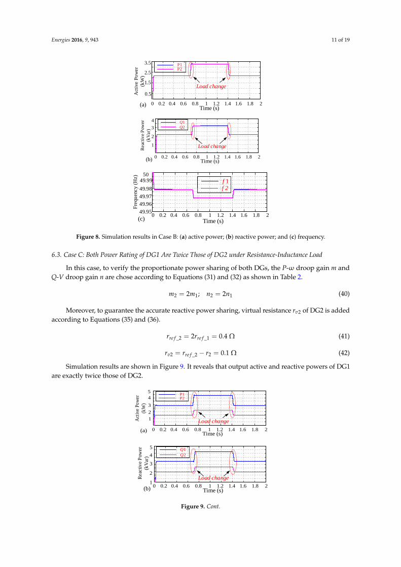
6.3. Case C: Both Power Rating of DG1 Are Twice Those of DG2 under Resistance-Inductance Load
In this case, to verify the proportionate power sharing of both DGs, the P-ω droop gain m and
Q-V droop gain n are chose according to Equations (31) and (32) as shown in Table 2.
2 1 2 12 ; 2 m m n n (40)
Moreover, to guarantee the accurate reactive power sharing, virtual resistance rv2 of DG2 is
added according to Equations (35) and (36).
_ 2 _12 = 0.4 ref refr r (41)
2 _ 2 2 = 0.1 v refr r r (42)
Simulation results are shown in Figure 9. It reveals that output active and reactive powers of
DG1 are exactly twice those of DG2.
1
2
3
4
5
Act
ive
Po
wer
(kW
)
Time (s)0 0.2 0.4 0.6 0.8 1 1.2 1.4 1.6 1.8 2
P1P2
Load change
(a)
2
3
4
5
Times (s)0 0.2 0.4 0.6 0.8 1 1.2 1.4 1.6 1.8 2
Q1
Q2
Rea
ctiv
e P
ower
(kV
ar)
(b)
Load change49.95
49.96
49.98
50
Fre
quen
cy (
Hz)
(c)
f 1f 2
Times (s)0 0.2 0.4 0.6 0.8 1 1.2 1.4 1.6 1.8 2
1
49.97
49.99
1
2
3
4
5
Act
ive
Po
wer
(kW
)
Times (s)0 0.2 0.4 0.6 0.8 1 1.2 1.4 1.6 1.8 2
P1P2
Load change
(a)
2
3
4
5
Time (s)0 0.2 0.4 0.6 0.8 1 1.2 1.4 1.6 1.8 2
Q1
Q2
Rea
ctiv
e P
ower
(kV
ar)
(b)
Load change49.95
49.96
49.98
50
Fre
quen
cy (
Hz)
(c)
f 1f 2
Times (s)0 0.2 0.4 0.6 0.8 1 1.2 1.4 1.6 1.8 2
1
49.97
49.99
0.5
1.5
2.5
3.5
Act
ive P
ow
er
(kW
)
Times (s)0 0.2 0.4 0.6 0.8 1 1.2 1.4 1.6 1.8 2
P1P2
Load change
(a)
1
2
3
4
Time (s)0 0.2 0.4 0.6 0.8 1 1.2 1.4 1.6 1.8 2
Q1
Q2
Reac
tiv
e P
ow
er
(kV
ar)
(b)
Load change
49.95
49.96
50
Fre
qu
ency (
Hz)
(c)
f 1f 2
Times (s)0 0.2 0.4 0.6 0.8 1 1.2 1.4 1.6 1.8 2
49.99
49.98
49.97
0.5
1.5
2.5
3.5
Act
ive P
ow
er
(kW
)
Times (s)0 0.2 0.4 0.6 0.8 1 1.2 1.4 1.6 1.8 2
P1P2
Load change
(a)
1
2
3
4
Times (s)0 0.2 0.4 0.6 0.8 1 1.2 1.4 1.6 1.8 2
Q1
Q2
Reac
tiv
e P
ow
er
(kV
ar)
(b)
Load change
49.95
49.96
50
Fre
qu
ency (
Hz)
(c)
f 1f 2
Time (s)0 0.2 0.4 0.6 0.8 1 1.2 1.4 1.6 1.8 2
49.99
49.98
49.97
Figure 8. Simulation results in Case B: (a) active power; (b) reactive power; and (c) frequency.
6.3. Case C: Both Power Rating of DG1 Are Twice Those of DG2 under Resistance-Inductance Load
In this case, to verify the proportionate power sharing of both DGs, the P-ω droop gain m andQ-V droop gain n are chose according to Equations (31) and (32) as shown in Table 2.
m2 = 2m1; n2 = 2n1 (40)
Moreover, to guarantee the accurate reactive power sharing, virtual resistance rv2 of DG2 is addedaccording to Equations (35) and (36).
rre f _2 = 2rre f _1 = 0.4 Ω (41)
rv2 = rre f _2 − r2 = 0.1 Ω (42)
Simulation results are shown in Figure 9. It reveals that output active and reactive powers of DG1are exactly twice those of DG2.
Energies 2016, 9, 943 11 of 19
0.5
1.5
2.5
3.5
Act
ive P
ow
er
(kW
)
Time (s)0 0.2 0.4 0.6 0.8 1 1.2 1.4 1.6 1.8 2
P1P2
Load change
(a)
1
2
3
4
Times (s)0 0.2 0.4 0.6 0.8 1 1.2 1.4 1.6 1.8 2
Q1
Q2
Reac
tiv
e P
ow
er
(kV
ar)
(b)
Load change
49.95
49.96
50
Fre
qu
ency (
Hz)
(c)
f 1f 2
Times (s)0 0.2 0.4 0.6 0.8 1 1.2 1.4 1.6 1.8 2
49.99
49.98
49.97
Figure 8. Simulation results in Case B: (a) active power; (b) reactive power; and (c) frequency.
6.3. Case C: Both Power Rating of DG1 Are Twice Those of DG2 under Resistance-Inductance Load
In this case, to verify the proportionate power sharing of both DGs, the P-ω droop gain m and
Q-V droop gain n are chose according to Equations (31) and (32) as shown in Table 2.
2 1 2 12 ; 2 m m n n (40)
Moreover, to guarantee the accurate reactive power sharing, virtual resistance rv2 of DG2 is
added according to Equations (35) and (36).
_ 2 _12 = 0.4 ref refr r (41)
2 _ 2 2 = 0.1 v refr r r (42)
Simulation results are shown in Figure 9. It reveals that output active and reactive powers of
DG1 are exactly twice those of DG2.
1
2
3
4
5
Act
ive
Po
wer
(kW
)
Time (s)0 0.2 0.4 0.6 0.8 1 1.2 1.4 1.6 1.8 2
P1P2
Load change
(a)
2
3
4
5
Times (s)0 0.2 0.4 0.6 0.8 1 1.2 1.4 1.6 1.8 2
Q1
Q2
Rea
ctiv
e P
ower
(kV
ar)
(b)
Load change49.95
49.96
49.98
50
Fre
quen
cy (
Hz)
(c)
f 1f 2
Times (s)0 0.2 0.4 0.6 0.8 1 1.2 1.4 1.6 1.8 2
1
49.97
49.99
1
2
3
4
5
Act
ive
Po
wer
(kW
)
Times (s)0 0.2 0.4 0.6 0.8 1 1.2 1.4 1.6 1.8 2
P1P2
Load change
(a)
2
3
4
5
Time (s)0 0.2 0.4 0.6 0.8 1 1.2 1.4 1.6 1.8 2
Q1
Q2
Rea
ctiv
e P
ower
(kV
ar)
(b)
Load change49.95
49.96
49.98
50
Fre
quen
cy (
Hz)
(c)
f 1f 2
Times (s)0 0.2 0.4 0.6 0.8 1 1.2 1.4 1.6 1.8 2
1
49.97
49.99
0.5
1.5
2.5
3.5
Act
ive P
ow
er
(kW
)
Times (s)0 0.2 0.4 0.6 0.8 1 1.2 1.4 1.6 1.8 2
P1P2
Load change
(a)
1
2
3
4
Time (s)0 0.2 0.4 0.6 0.8 1 1.2 1.4 1.6 1.8 2
Q1
Q2
Reac
tiv
e P
ow
er
(kV
ar)
(b)
Load change
49.95
49.96
50
Fre
qu
ency (
Hz)
(c)
f 1f 2
Times (s)0 0.2 0.4 0.6 0.8 1 1.2 1.4 1.6 1.8 2
49.99
49.98
49.97
0.5
1.5
2.5
3.5
Act
ive P
ow
er
(kW
)
Times (s)0 0.2 0.4 0.6 0.8 1 1.2 1.4 1.6 1.8 2
P1P2
Load change
(a)
1
2
3
4
Times (s)0 0.2 0.4 0.6 0.8 1 1.2 1.4 1.6 1.8 2
Q1
Q2
Reac
tiv
e P
ow
er
(kV
ar)
(b)
Load change
49.95
49.96
50
Fre
qu
ency (
Hz)
(c)
f 1f 2
Time (s)0 0.2 0.4 0.6 0.8 1 1.2 1.4 1.6 1.8 2
49.99
49.98
49.97
Figure 9. Cont.
Energies 2016, 9, 943 12 of 19Energies 2016, 9, 943 12 of 19
1
2
3
4
5
Act
ive
Po
wer
(kW
)
Times (s)0 0.2 0.4 0.6 0.8 1 1.2 1.4 1.6 1.8 2
P1P2
Load change
(a)
2
3
4
5
Times (s)0 0.2 0.4 0.6 0.8 1 1.2 1.4 1.6 1.8 2
Q1
Q2
Rea
ctiv
e P
ower
(kV
ar)
(b)
Load change49.95
49.96
49.98
50
Fre
quen
cy (
Hz)
(c)
f 1f 2
Time (s)0 0.2 0.4 0.6 0.8 1 1.2 1.4 1.6 1.8 2
1
49.97
49.99
Figure 9. Simulation results in Case C: (a) active power; (b) reactive power; and (c) frequency.
6.4. Case D: Two DGs with the Same Power Rating under Resistance-Capacitance Load
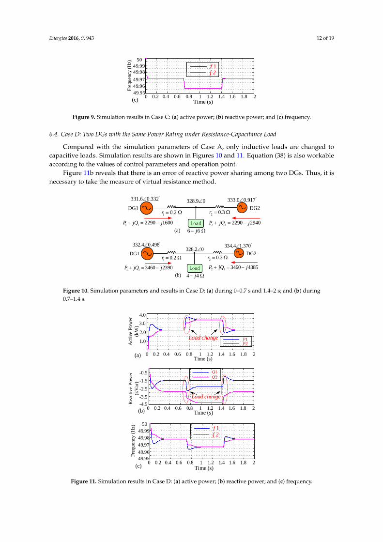
Compared with the simulation parameters of Case A, only inductive loads are changed to
capacitive loads. Simulation results are shown in Figures 10 and 11. Equation (38) is also workable
according to the values of control parameters and operation point.
Figure 11b reveals that there is an error of reactive power sharing among two DGs. Thus, it is
necessary to take the measure of virtual resistance method.
Load
328.9 0331.6 0.332 333.0 0.917
1 1 2290 1600P jQ j
2 0.3 r 1 0.2 r
6 6 j
2 2 2290 2940P jQ j Load
328.2 0332.4 0.498 334.4 1.370
1 1 3460 2390P jQ j
2 0.3 r 1 0.2 r
4 4 j
2 2 3460 4385P jQ j
(a) (b)
DG1 DG1DG2 DG2
Load
328.9 0331.6 0.332 333.0 0.917
1 1 2290 1600P jQ j
2 0.3 r 1 0.2 r
6 6 j
2 2 2290 2940P jQ j Load
328.2 0332.4 0.498 334.4 1.370
1 1 3460 2390P jQ j
2 0.3 r 1 0.2 r
4 4 j
2 2 3460 4385P jQ j
(a) (b)
DG1 DG1DG2 DG2
Figure 10. Simulation parameters and results in Case D: (a) during 0–0.7 s and 1.4–2 s; and (b) during 0.7–1.4 s.
1.0
2.0
3.0
4.0
Act
ive P
ow
er
(kW
)
Time (s)0 0.2 0.4 0.6 0.8 1 1.2 1.4 1.6 1.8 2
P1P2
Load change
(a)-4.5
-2.5
-0.5
Times (s)0 0.2 0.4 0.6 0.8 1 1.2 1.4 1.6 1.8 2
Q1
Q2
Reac
tiv
e P
ow
er
(kV
ar)
(b)
Load change
49.95
49.96
49.97
50
Fre
qu
ency (
Hz)
(c)
f 1f 2
Times (s)0 0.2 0.4 0.6 0.8 1 1.2 1.4 1.6 1.8 2
-3.5
-1.549.98
49.99
1.0
2.0
3.0
4.0
Act
ive P
ow
er
(kW
)
Times (s)0 0.2 0.4 0.6 0.8 1 1.2 1.4 1.6 1.8 2
P1P2
Load change
(a)-4.5
-2.5
-0.5
Time (s)0 0.2 0.4 0.6 0.8 1 1.2 1.4 1.6 1.8 2
Q1
Q2
Reac
tiv
e P
ow
er
(kV
ar)
(b)
Load change
49.95
49.96
49.97
50
Fre
qu
ency (
Hz)
(c)
f 1f 2
Times (s)0 0.2 0.4 0.6 0.8 1 1.2 1.4 1.6 1.8 2
-3.5
-1.549.98
49.99
1.0
2.0
3.0
4.0
Act
ive P
ow
er
(kW
)
Times (s)0 0.2 0.4 0.6 0.8 1 1.2 1.4 1.6 1.8 2
P1P2
Load change
(a)-4.5
-2.5
-0.5
Times (s)0 0.2 0.4 0.6 0.8 1 1.2 1.4 1.6 1.8 2
Q1
Q2
Reac
tiv
e P
ow
er
(kV
ar)
(b)
Load change
49.95
49.96
49.97
50
Fre
qu
ency (
Hz)
(c)
f 1f 2
Time (s)0 0.2 0.4 0.6 0.8 1 1.2 1.4 1.6 1.8 2
-3.5
-1.549.98
49.99
Figure 11. Simulation results in Case D: (a) active power; (b) reactive power; and (c) frequency.
Figure 9. Simulation results in Case C: (a) active power; (b) reactive power; and (c) frequency.
6.4. Case D: Two DGs with the Same Power Rating under Resistance-Capacitance Load
Compared with the simulation parameters of Case A, only inductive loads are changed tocapacitive loads. Simulation results are shown in Figures 10 and 11. Equation (38) is also workableaccording to the values of control parameters and operation point.
Figure 11b reveals that there is an error of reactive power sharing among two DGs. Thus, it isnecessary to take the measure of virtual resistance method.
Energies 2016, 9, 943 12 of 19
1
2
3
4
5
Act
ive
Po
wer
(kW
)
Times (s)0 0.2 0.4 0.6 0.8 1 1.2 1.4 1.6 1.8 2
P1P2
Load change
(a)
2
3
4
5
Times (s)0 0.2 0.4 0.6 0.8 1 1.2 1.4 1.6 1.8 2
Q1
Q2
Rea
ctiv
e P
ower
(kV
ar)
(b)
Load change49.95
49.96
49.98
50
Fre
quen
cy (
Hz)
(c)
f 1f 2
Time (s)0 0.2 0.4 0.6 0.8 1 1.2 1.4 1.6 1.8 2
1
49.97
49.99
Figure 9. Simulation results in Case C: (a) active power; (b) reactive power; and (c) frequency.
6.4. Case D: Two DGs with the Same Power Rating under Resistance-Capacitance Load
Compared with the simulation parameters of Case A, only inductive loads are changed to
capacitive loads. Simulation results are shown in Figures 10 and 11. Equation (38) is also workable
according to the values of control parameters and operation point.
Figure 11b reveals that there is an error of reactive power sharing among two DGs. Thus, it is
necessary to take the measure of virtual resistance method.
Load
328.9 0331.6 0.332 333.0 0.917
1 1 2290 1600P jQ j
2 0.3 r 1 0.2 r
6 6 j
2 2 2290 2940P jQ j Load
328.2 0332.4 0.498 334.4 1.370
1 1 3460 2390P jQ j
2 0.3 r 1 0.2 r
4 4 j
2 2 3460 4385P jQ j
(a) (b)
DG1 DG1DG2 DG2
Load
328.9 0331.6 0.332 333.0 0.917
1 1 2290 1600P jQ j
2 0.3 r 1 0.2 r
6 6 j
2 2 2290 2940P jQ j Load
328.2 0332.4 0.498 334.4 1.370
1 1 3460 2390P jQ j
2 0.3 r 1 0.2 r
4 4 j
2 2 3460 4385P jQ j
(a) (b)
DG1 DG1DG2 DG2
Figure 10. Simulation parameters and results in Case D: (a) during 0–0.7 s and 1.4–2 s; and (b) during 0.7–1.4 s.
1.0
2.0
3.0
4.0
Act
ive P
ow
er
(kW
)
Time (s)0 0.2 0.4 0.6 0.8 1 1.2 1.4 1.6 1.8 2
P1P2
Load change
(a)-4.5
-2.5
-0.5
Times (s)0 0.2 0.4 0.6 0.8 1 1.2 1.4 1.6 1.8 2
Q1
Q2
Reac
tiv
e P
ow
er
(kV
ar)
(b)
Load change
49.95
49.96
49.97
50
Fre
qu
ency (
Hz)
(c)
f 1f 2
Times (s)0 0.2 0.4 0.6 0.8 1 1.2 1.4 1.6 1.8 2
-3.5
-1.549.98
49.99
1.0
2.0
3.0
4.0
Act
ive P
ow
er
(kW
)
Times (s)0 0.2 0.4 0.6 0.8 1 1.2 1.4 1.6 1.8 2
P1P2
Load change
(a)-4.5
-2.5
-0.5
Time (s)0 0.2 0.4 0.6 0.8 1 1.2 1.4 1.6 1.8 2
Q1
Q2
Reac
tiv
e P
ow
er
(kV
ar)
(b)
Load change
49.95
49.96
49.97
50
Fre
qu
ency (
Hz)
(c)
f 1f 2
Times (s)0 0.2 0.4 0.6 0.8 1 1.2 1.4 1.6 1.8 2
-3.5
-1.549.98
49.99
1.0
2.0
3.0
4.0
Act
ive P
ow
er
(kW
)
Times (s)0 0.2 0.4 0.6 0.8 1 1.2 1.4 1.6 1.8 2
P1P2
Load change
(a)-4.5
-2.5
-0.5
Times (s)0 0.2 0.4 0.6 0.8 1 1.2 1.4 1.6 1.8 2
Q1
Q2
Reac
tiv
e P
ow
er
(kV
ar)
(b)
Load change
49.95
49.96
49.97
50
Fre
qu
ency (
Hz)
(c)
f 1f 2
Time (s)0 0.2 0.4 0.6 0.8 1 1.2 1.4 1.6 1.8 2
-3.5
-1.549.98
49.99
Figure 11. Simulation results in Case D: (a) active power; (b) reactive power; and (c) frequency.
Figure 10. Simulation parameters and results in Case D: (a) during 0–0.7 s and 1.4–2 s; and (b) during0.7–1.4 s.
Energies 2016, 9, 943 12 of 19
1
2
3
4
5
Act
ive
Po
wer
(kW
)
Times (s)0 0.2 0.4 0.6 0.8 1 1.2 1.4 1.6 1.8 2
P1P2
Load change
(a)
2
3
4
5
Times (s)0 0.2 0.4 0.6 0.8 1 1.2 1.4 1.6 1.8 2
Q1
Q2
Rea
ctiv
e P
ower
(kV
ar)
(b)
Load change49.95
49.96
49.98
50
Fre
quen
cy (
Hz)
(c)
f 1f 2
Time (s)0 0.2 0.4 0.6 0.8 1 1.2 1.4 1.6 1.8 2
1
49.97
49.99
Figure 9. Simulation results in Case C: (a) active power; (b) reactive power; and (c) frequency.
6.4. Case D: Two DGs with the Same Power Rating under Resistance-Capacitance Load
Compared with the simulation parameters of Case A, only inductive loads are changed to
capacitive loads. Simulation results are shown in Figures 10 and 11. Equation (38) is also workable
according to the values of control parameters and operation point.
Figure 11b reveals that there is an error of reactive power sharing among two DGs. Thus, it is
necessary to take the measure of virtual resistance method.
Load
328.9 0331.6 0.332 333.0 0.917
1 1 2290 1600P jQ j
2 0.3 r 1 0.2 r
6 6 j
2 2 2290 2940P jQ j Load
328.2 0332.4 0.498 334.4 1.370
1 1 3460 2390P jQ j
2 0.3 r 1 0.2 r
4 4 j
2 2 3460 4385P jQ j
(a) (b)
DG1 DG1DG2 DG2
Load
328.9 0331.6 0.332 333.0 0.917
1 1 2290 1600P jQ j
2 0.3 r 1 0.2 r
6 6 j
2 2 2290 2940P jQ j Load
328.2 0332.4 0.498 334.4 1.370
1 1 3460 2390P jQ j
2 0.3 r 1 0.2 r
4 4 j
2 2 3460 4385P jQ j
(a) (b)
DG1 DG1DG2 DG2
Figure 10. Simulation parameters and results in Case D: (a) during 0–0.7 s and 1.4–2 s; and (b) during 0.7–1.4 s.
1.0
2.0
3.0
4.0
Act
ive P
ow
er
(kW
)
Time (s)0 0.2 0.4 0.6 0.8 1 1.2 1.4 1.6 1.8 2
P1P2
Load change
(a)-4.5
-2.5
-0.5
Times (s)0 0.2 0.4 0.6 0.8 1 1.2 1.4 1.6 1.8 2
Q1
Q2
Reac
tiv
e P
ow
er
(kV
ar)
(b)
Load change
49.95
49.96
49.97
50
Fre
qu
ency (
Hz)
(c)
f 1f 2
Times (s)0 0.2 0.4 0.6 0.8 1 1.2 1.4 1.6 1.8 2
-3.5
-1.549.98
49.99
1.0
2.0
3.0
4.0
Act
ive P
ow
er
(kW
)
Times (s)0 0.2 0.4 0.6 0.8 1 1.2 1.4 1.6 1.8 2
P1P2
Load change
(a)-4.5
-2.5
-0.5
Time (s)0 0.2 0.4 0.6 0.8 1 1.2 1.4 1.6 1.8 2
Q1
Q2
Reac
tiv
e P
ow
er
(kV
ar)
(b)
Load change
49.95
49.96
49.97
50
Fre
qu
ency (
Hz)
(c)
f 1f 2
Times (s)0 0.2 0.4 0.6 0.8 1 1.2 1.4 1.6 1.8 2
-3.5
-1.549.98
49.99
1.0
2.0
3.0
4.0
Act
ive P
ow
er
(kW
)
Times (s)0 0.2 0.4 0.6 0.8 1 1.2 1.4 1.6 1.8 2
P1P2
Load change
(a)-4.5
-2.5
-0.5
Times (s)0 0.2 0.4 0.6 0.8 1 1.2 1.4 1.6 1.8 2
Q1
Q2
Reac
tiv
e P
ow
er
(kV
ar)
(b)
Load change
49.95
49.96
49.97
50
Fre
qu
ency (
Hz)
(c)
f 1f 2
Time (s)0 0.2 0.4 0.6 0.8 1 1.2 1.4 1.6 1.8 2
-3.5
-1.549.98
49.99
Figure 11. Simulation results in Case D: (a) active power; (b) reactive power; and (c) frequency. Figure 11. Simulation results in Case D: (a) active power; (b) reactive power; and (c) frequency.

Energies 2016, 9, 943 13 of 19
6.5. Case E: Virtual Resistance of DG1 to Improve Reactive Power Sharing under Resistance-Capacitance Load
Similar to the virtual resistance method of Case B, virtual resistance rv1 = 0.1 Ω of DG1 is addedaccording to Equations (35) and (36). Simulation results are shown in Figure 12. Compared withFigure 11b, the reactive power sharing difference between two DGs is greatly reduced, which verifiesthe effectiveness of virtual resistance under RC loads.
Energies 2016, 9, 943 13 of 19
6.5. Case E: Virtual Resistance of DG1 to Improve Reactive Power Sharing under Resistance-Capacitance Load
Similar to the virtual resistance method of Case B, virtual resistance rv1 = 0.1 Ω of DG1 is added
according to Equations (35) and (36). Simulation results are shown in Figure 12. Compared with
Figure 11b, the reactive power sharing difference between two DGs is greatly reduced, which
verifies the effectiveness of virtual resistance under RC loads.
0.5
1.5
2.5
3.5
Act
ive P
ow
er
(kW
)
Time (s)0 0.2 0.4 0.6 0.8 1 1.2 1.4 1.6 1.8 2
P1P2
Load change
(a)-4
-2
0
Time (s)0 0.2 0.4 0.6 0.8 1 1.2 1.4 1.6 1.8 2
Q1
Q2
Reac
tiv
e P
ow
er
(kV
ar)
(b)
Load change
49.95
49.96
49.97
50
Fre
qu
ency (
Hz)
(c)
f 1f 2
Time (s)0 0.2 0.4 0.6 0.8 1 1.2 1.4 1.6 1.8 2
-3
-149.98
49.99
0.5
1.5
2.5
3.5
Act
ive P
ow
er
(kW
)
Times (s)0 0.2 0.4 0.6 0.8 1 1.2 1.4 1.6 1.8 2
P1P2
Load change
(a)-4
-2
0
Time (s)0 0.2 0.4 0.6 0.8 1 1.2 1.4 1.6 1.8 2
Q1
Q2
Reac
tiv
e P
ow
er
(kV
ar)
(b)
Load change
49.95
49.96
49.97
50
Fre
qu
ency (
Hz)
(c)
f 1f 2
Times (s)0 0.2 0.4 0.6 0.8 1 1.2 1.4 1.6 1.8 2
-3
-149.98
49.99
0.5
1.5
2.5
3.5
Act
ive P
ow
er
(kW
)
Times (s)0 0.2 0.4 0.6 0.8 1 1.2 1.4 1.6 1.8 2
P1P2
Load change
(a)-4
-2
0
Times (s)0 0.2 0.4 0.6 0.8 1 1.2 1.4 1.6 1.8 2
Q1
Q2
Reac
tiv
e P
ow
er
(kV
ar)
(b)
Load change
49.95
49.96
49.97
50
Fre
qu
ency (
Hz)
(c)
f 1f 2
Time (s)0 0.2 0.4 0.6 0.8 1 1.2 1.4 1.6 1.8 2
-3
-149.98
49.99
Figure 12. Simulation results in Case E: (a) active power; (b) reactive power; and (c) frequency.
6.6. Case F: Validity of Conventional Droop Control in Highly Resistive Line of AC Microgrid
In this case, the validity of conventional droop control is tested in the line parameters of
low-voltage AC microgrid as presented in Table 1. The line lengths of DG1 and DG2 are 400 m and
600 m, respectively. From the simulation results in Figures 13 and 14, the conventional droop control
is quite applicable for the highly resistive line of AC microgrid.
As the line character is mainly resistive (R >> X) in low voltage microgrid, the above analysis
and simulations are reasonable by neglecting the minor line reactance and treating the highly
resistive line as pure resistance.
Load
322.2 0327.8 0.554 327.9 0.768
1 1 2165 2210P jQ j
600m400m
6 6 j
2 2 2165 2100P jQ j
4 4 j (a) (b)
DG1 DG21 0.2568 0.0332 r j
2 0.3852 0.0498 r j
Load
318.4 0326.8 0.808 326.9 1.141
1 1 3250 3240P jQ j
600m400m
2 2 3250 3090P jQ j
DG1 DG21 0.2568 0.0332 r j
2 0.3852 0.0498 r j
Load
322.2 0327.8 0.554 327.9 0.768
1 1 2165 2210P jQ j
600m400m
6 6 j
2 2 2165 2100P jQ j
4 4 j (a) (b)
DG1 DG21 0.2568 0.0332 r j
2 0.3852 0.0498 r j
Load
318.4 0326.8 0.808 326.9 1.141
1 1 3250 3240P jQ j
600m400m
2 2 3250 3090P jQ j
DG1 DG21 0.2568 0.0332 r j
2 0.3852 0.0498 r j
Figure 13. Simulation parameters and results in Case F: (a) during 0–0.7 s and 1.4–2 s; and (b) during
0.7–1.4 s.
Figure 12. Simulation results in Case E: (a) active power; (b) reactive power; and (c) frequency.
6.6. Case F: Validity of Conventional Droop Control in Highly Resistive Line of AC Microgrid
In this case, the validity of conventional droop control is tested in the line parameters oflow-voltage AC microgrid as presented in Table 1. The line lengths of DG1 and DG2 are 400 mand 600 m, respectively. From the simulation results in Figures 13 and 14, the conventional droopcontrol is quite applicable for the highly resistive line of AC microgrid.
As the line character is mainly resistive (R >> X) in low voltage microgrid, the above analysis andsimulations are reasonable by neglecting the minor line reactance and treating the highly resistive lineas pure resistance.
Energies 2016, 9, 943 13 of 19
6.5. Case E: Virtual Resistance of DG1 to Improve Reactive Power Sharing under Resistance-Capacitance Load
Similar to the virtual resistance method of Case B, virtual resistance rv1 = 0.1 Ω of DG1 is added
according to Equations (35) and (36). Simulation results are shown in Figure 12. Compared with
Figure 11b, the reactive power sharing difference between two DGs is greatly reduced, which
verifies the effectiveness of virtual resistance under RC loads.
0.5
1.5
2.5
3.5A
ctiv
e P
ow
er
(kW
)
Time (s)0 0.2 0.4 0.6 0.8 1 1.2 1.4 1.6 1.8 2
P1P2
Load change
(a)-4
-2
0
Time (s)0 0.2 0.4 0.6 0.8 1 1.2 1.4 1.6 1.8 2
Q1
Q2
Reac
tiv
e P
ow
er
(kV
ar)
(b)
Load change
49.95
49.96
49.97
50
Fre
qu
ency (
Hz)
(c)
f 1f 2
Time (s)0 0.2 0.4 0.6 0.8 1 1.2 1.4 1.6 1.8 2
-3
-149.98
49.99
0.5
1.5
2.5
3.5
Act
ive P
ow
er
(kW
)
Times (s)0 0.2 0.4 0.6 0.8 1 1.2 1.4 1.6 1.8 2
P1P2
Load change
(a)-4
-2
0
Time (s)0 0.2 0.4 0.6 0.8 1 1.2 1.4 1.6 1.8 2
Q1
Q2
Reac
tiv
e P
ow
er
(kV
ar)
(b)
Load change
49.95
49.96
49.97
50
Fre
qu
ency (
Hz)
(c)
f 1f 2
Times (s)0 0.2 0.4 0.6 0.8 1 1.2 1.4 1.6 1.8 2
-3
-149.98
49.99
0.5
1.5
2.5
3.5
Act
ive P
ow
er
(kW
)
Times (s)0 0.2 0.4 0.6 0.8 1 1.2 1.4 1.6 1.8 2
P1P2
Load change
(a)-4
-2
0
Times (s)0 0.2 0.4 0.6 0.8 1 1.2 1.4 1.6 1.8 2
Q1
Q2
Reac
tiv
e P
ow
er
(kV
ar)
(b)
Load change
49.95
49.96
49.97
50
Fre
qu
ency (
Hz)
(c)
f 1f 2
Time (s)0 0.2 0.4 0.6 0.8 1 1.2 1.4 1.6 1.8 2
-3
-149.98
49.99
Figure 12. Simulation results in Case E: (a) active power; (b) reactive power; and (c) frequency.
6.6. Case F: Validity of Conventional Droop Control in Highly Resistive Line of AC Microgrid
In this case, the validity of conventional droop control is tested in the line parameters of
low-voltage AC microgrid as presented in Table 1. The line lengths of DG1 and DG2 are 400 m and
600 m, respectively. From the simulation results in Figures 13 and 14, the conventional droop control
is quite applicable for the highly resistive line of AC microgrid.
As the line character is mainly resistive (R >> X) in low voltage microgrid, the above analysis
and simulations are reasonable by neglecting the minor line reactance and treating the highly
resistive line as pure resistance.
Load
322.2 0327.8 0.554 327.9 0.768
1 1 2165 2210P jQ j
600m400m
6 6 j
2 2 2165 2100P jQ j
4 4 j (a) (b)
DG1 DG21 0.2568 0.0332 r j
2 0.3852 0.0498 r j
Load
318.4 0326.8 0.808 326.9 1.141
1 1 3250 3240P jQ j
600m400m
2 2 3250 3090P jQ j
DG1 DG21 0.2568 0.0332 r j
2 0.3852 0.0498 r j
Load
322.2 0327.8 0.554 327.9 0.768
1 1 2165 2210P jQ j
600m400m
6 6 j
2 2 2165 2100P jQ j
4 4 j (a) (b)
DG1 DG21 0.2568 0.0332 r j
2 0.3852 0.0498 r j
Load
318.4 0326.8 0.808 326.9 1.141
1 1 3250 3240P jQ j
600m400m
2 2 3250 3090P jQ j
DG1 DG21 0.2568 0.0332 r j
2 0.3852 0.0498 r j
Figure 13. Simulation parameters and results in Case F: (a) during 0–0.7 s and 1.4–2 s; and (b) during
0.7–1.4 s. Figure 13. Simulation parameters and results in Case F: (a) during 0–0.7 s and 1.4–2 s; and (b) during0.7–1.4 s.

Energies 2016, 9, 943 14 of 19
Energies 2016, 9, 943 14 of 19
0.5
11.52
2.53
3.5
P1P2A
ctiv
e P
ow
er
(kW
)Load change
0 0.2 0.4 0.6 0.8 1 1.2 1.4 1.6 1.8 2(a)
Time (s)
0
1
2
3
4
Q1
Q2 Load change
0 0.2 0.4 0.6 0.8 1 1.2 1.4 1.6 1.8 2
Rea
ctiv
e P
ower
(kV
ar)
(b)
Time (s)
-25
-20
-15
-10
-5
0
0 0.2 0.4 0.6 0.8 1 1.2 1.4 1.6 1.8 2
Po
wer
Ang
le
(rad
)
(c)
x 10-3
Time (s)
Fre
qu
ency
(H
z)
49.95
49.96
49.97
49.98
49.99
50f 1f 2
(d) Time (s)0 0.2 0.4 0.6 0.8 1 1.2 1.4 1.6 1.8 2
325
326
327
328
329
330
Volt
age
(V)
Time (s)0 0.2 0.4 0.6 0.8 1 1.2 1.4 1.6 1.8 2
V1V2
(e)
0.5
11.5
P1P2A
ctiv
e P
ow
er
(kW
Load change
0 0.2 0.4 0.6 0.8 1 1.2 1.4 1.6 1.8 2(a)
0
1
2
3
4
Q1
Q2 Load change
0 0.2 0.4 0.6 0.8 1 1.2 1.4 1.6 1.8 2
Rea
ctiv
e P
ower
(kV
ar)
(b)
-350
-200
0
200
350
Time (s)0.6 0.7 0.8
Vol
tag
e/ C
urr
en
t
(V)/
(A)
(f)
v1i1
Fre
quen
cy (
Hz)
49.95
49.96
49.97
49.98
49.99
50f 1f 2
(d) Time (s)0 0.2 0.4 0.6 0.8 1 1.2 1.4 1.6 1.8 2
326
327
328
329
330
Volt
age
(V) V1
V2
Time (s)
Time (s)
-25
-20
-15
-10
0 0.2 0.4 0.6 0.8 1 1.2 1.4 1.6 1.8 2
Po
wer
Ang
le
(rad
)
(c)
Time (s)
Figure 14. Simulation results in Case F: (a) active power; (b) reactive power; (c) power angle; (d)
frequency; (e) voltage amplitude; and (f) voltage and current of DG1.
7. Experiment Results
A converter-based microgrid prototype is built in lab as shown in Figure 15. The microgrid
consists of two micro-sources based on single-phase inverter. The main circuits are shown in Figure
16, which includes the experiment parameters for output filter, line, and load. The sample frequency
is 12.8 kHz. The referent voltage frequency f* and amplitude V* are 50 Hz and 48 V, respectively.
Figure 15. Prototype of parallel inverters system setup.
1lineR
1u
fL
fC
dcV
60V
1i
1mH
22 F
2lineR
2u
fL
fC
dcV
60V
2i
1mH
22 F
0.5
1
10
16mH
DG1
DG2
Figure 16. Main circuits of the experiment system.
Figure 14. Simulation results in Case F: (a) active power; (b) reactive power; (c) power angle;(d) frequency; (e) voltage amplitude; and (f) voltage and current of DG1.
7. Experiment Results
A converter-based microgrid prototype is built in lab as shown in Figure 15. The microgridconsists of two micro-sources based on single-phase inverter. The main circuits are shown in Figure 16,which includes the experiment parameters for output filter, line, and load. The sample frequency is12.8 kHz. The referent voltage frequency f * and amplitude V* are 50 Hz and 48 V, respectively.
Energies 2016, 9, 943 14 of 19
0.5
11.52
2.53
3.5
P1P2A
ctiv
e P
ow
er
(kW
)
Load change
0 0.2 0.4 0.6 0.8 1 1.2 1.4 1.6 1.8 2(a)
Time (s)
0
1
2
3
4
Q1
Q2 Load change
0 0.2 0.4 0.6 0.8 1 1.2 1.4 1.6 1.8 2
Rea
ctiv
e P
ower
(kV
ar)
(b)
Time (s)
-25
-20
-15
-10
-5
0
0 0.2 0.4 0.6 0.8 1 1.2 1.4 1.6 1.8 2
Po
wer
Ang
le
(rad
)
(c)
x 10-3
Time (s)
Fre
qu
ency
(H
z)
49.95
49.96
49.97
49.98
49.99
50f 1f 2
(d) Time (s)0 0.2 0.4 0.6 0.8 1 1.2 1.4 1.6 1.8 2
325
326
327
328
329
330
Volt
age
(V)
Time (s)0 0.2 0.4 0.6 0.8 1 1.2 1.4 1.6 1.8 2
V1V2
(e)
0.5
11.5
P1P2A
ctiv
e P
ow
er
(kW
Load change
0 0.2 0.4 0.6 0.8 1 1.2 1.4 1.6 1.8 2(a)
0
1
2
3
4
Q1
Q2 Load change
0 0.2 0.4 0.6 0.8 1 1.2 1.4 1.6 1.8 2
Rea
ctiv
e P
ower
(kV
ar)
(b)
-350
-200
0
200
350
Time (s)0.6 0.7 0.8
Vol
tag
e/ C
urr
en
t
(V)/
(A)
(f)
v1i1
Fre
quen
cy (
Hz)
49.95
49.96
49.97
49.98
49.99
50f 1f 2
(d) Time (s)0 0.2 0.4 0.6 0.8 1 1.2 1.4 1.6 1.8 2
326
327
328
329
330
Volt
age
(V) V1
V2
Time (s)
Time (s)
-25
-20
-15
-10
0 0.2 0.4 0.6 0.8 1 1.2 1.4 1.6 1.8 2
Po
wer
Ang
le
(rad
)
(c)
Time (s)
Figure 14. Simulation results in Case F: (a) active power; (b) reactive power; (c) power angle; (d)
frequency; (e) voltage amplitude; and (f) voltage and current of DG1.
7. Experiment Results
A converter-based microgrid prototype is built in lab as shown in Figure 15. The microgrid
consists of two micro-sources based on single-phase inverter. The main circuits are shown in Figure
16, which includes the experiment parameters for output filter, line, and load. The sample frequency
is 12.8 kHz. The referent voltage frequency f* and amplitude V* are 50 Hz and 48 V, respectively.
Figure 15. Prototype of parallel inverters system setup.
1lineR
1u
fL
fC
dcV
60V
1i
1mH
22 F
2lineR
2u
fL
fC
dcV
60V
2i
1mH
22 F
0.5
1
10
16mH
DG1
DG2
Figure 16. Main circuits of the experiment system.
Figure 15. Prototype of parallel inverters system setup.
Energies 2016, 9, 943 14 of 19
0.5
11.52
2.53
3.5
P1P2A
ctiv
e P
ow
er
(kW
)Load change
0 0.2 0.4 0.6 0.8 1 1.2 1.4 1.6 1.8 2(a)
Time (s)
0
1
2
3
4
Q1
Q2 Load change
0 0.2 0.4 0.6 0.8 1 1.2 1.4 1.6 1.8 2
Rea
ctiv
e P
ower
(kV
ar)
(b)
Time (s)
-25
-20
-15
-10
-5
0
0 0.2 0.4 0.6 0.8 1 1.2 1.4 1.6 1.8 2
Po
wer
Ang
le
(rad
)
(c)
x 10-3
Time (s)
Fre
qu
ency
(H
z)
49.95
49.96
49.97
49.98
49.99
50f 1f 2
(d) Time (s)0 0.2 0.4 0.6 0.8 1 1.2 1.4 1.6 1.8 2
325
326
327
328
329
330
Volt
age
(V)
Time (s)0 0.2 0.4 0.6 0.8 1 1.2 1.4 1.6 1.8 2
V1V2
(e)
0.5
11.5
P1P2A
ctiv
e P
ow
er
(kW
Load change
0 0.2 0.4 0.6 0.8 1 1.2 1.4 1.6 1.8 2(a)
0
1
2
3
4
Q1
Q2 Load change
0 0.2 0.4 0.6 0.8 1 1.2 1.4 1.6 1.8 2
Rea
ctiv
e P
ower
(kV
ar)
(b)
-350
-200
0
200
350
Time (s)0.6 0.7 0.8
Vol
tag
e/ C
urr
en
t
(V)/
(A)
(f)
v1i1
Fre
quen
cy (
Hz)
49.95
49.96
49.97
49.98
49.99
50f 1f 2
(d) Time (s)0 0.2 0.4 0.6 0.8 1 1.2 1.4 1.6 1.8 2
326
327
328
329
330
Volt
age
(V) V1
V2
Time (s)
Time (s)
-25
-20
-15
-10
0 0.2 0.4 0.6 0.8 1 1.2 1.4 1.6 1.8 2
Po
wer
Ang
le
(rad
)
(c)
Time (s)
Figure 14. Simulation results in Case F: (a) active power; (b) reactive power; (c) power angle; (d)
frequency; (e) voltage amplitude; and (f) voltage and current of DG1.
7. Experiment Results
A converter-based microgrid prototype is built in lab as shown in Figure 15. The microgrid
consists of two micro-sources based on single-phase inverter. The main circuits are shown in Figure
16, which includes the experiment parameters for output filter, line, and load. The sample frequency
is 12.8 kHz. The referent voltage frequency f* and amplitude V* are 50 Hz and 48 V, respectively.
Figure 15. Prototype of parallel inverters system setup.
1lineR
1u
fL
fC
dcV
60V
1i
1mH
22 F
2lineR
2u
fL
fC
dcV
60V
2i
1mH
22 F
0.5
1
10
16mH
DG1
DG2
Figure 16. Main circuits of the experiment system. Figure 16. Main circuits of the experiment system.

Energies 2016, 9, 943 15 of 19
7.1. Case I: Two DGs with the Same Power Rating
According to Equation (38), the droop gains m = 3.14 × 10⁻³ rad/W·s and n = 2 × 10⁻² V/Var areselected for two DGs. Figure 17 shows the measured waveforms with the conventional droop controlmethods. The waveforms from top to down are the output voltage (U1) of inverter 1, the outputcurrent (I1) of inverter 1, the output voltage (U2) of inverter 2 and the output current (I2) of inverter 2.The voltage amplitudes of inverter 1 and 2 are 45.7 V and 46.4 V, respectively. The current amplitudesof inverter 1 and 2 are 2.16 A and 1.65 A, respectively.
Energies 2016, 9, 943 15 of 19
7.1. Case I: Two DGs with the Same Power Rating
According to Equation (38), the droop gains m = 3.14 × 10⁻³ rad/W·s and n = 2 × 10⁻² V/Var are
selected for two DGs. Figure 17 shows the measured waveforms with the conventional droop
control methods. The waveforms from top to down are the output voltage (U1) of inverter 1, the
output current (I1) of inverter 1, the output voltage (U2) of inverter 2 and the output current (I2) of
inverter 2. The voltage amplitudes of inverter 1 and 2 are 45.7 V and 46.4 V, respectively. The current
amplitudes of inverter 1 and 2 are 2.16 A and 1.65 A, respectively.
I2
U1
I1
U2
(4A/div)
(50V/div)
(50V/div)
(4A/div)
Figure 17. Steady state experimental waveforms of Case I.
Figure 18 shows the steady-state output active and reactive power of each inverter with the
conventional droop control. The steady-state output active powers of the inverters are 36.6 W and
36.5 W, and the output reactive powers are 36.1 Var and 9.1 Var. When using conventional P-ω
droop control, no active power divergence appear since frequency is a global variable, i.e. same
frequency can be measured along the microgrid; however, voltage may drop along the microgrid
power lines, which produces the well know reactive power divergence.
50
40
30
20
10
0 0.5 1 1.5 2Time (s)
(a)
50
40
30
20
10
0 0.5 1 1.5 2Times (s)
(b)
Reac
tiv
e P
ow
er
(Var
)
Act
ive P
ow
er
(W)
P1 and P2 Q1
Q2
50
40
30
20
10
0 0.5 1 1.5 2Time (s)
(a)
50
40
30
20
10
0 0.5 1 1.5 2Time (s)
(b)
Reac
tiv
e P
ow
er
(Var
)
Act
ive P
ow
er
(W)
P1 and P2 Q1
Q2
Figure 18. Steady-state power of Case I: (a) active power; and (b) reactive power.
7.2. Case II: The Active Power Rating of DG1 Is Twice that for DG2
To investigate the proper active power sharing, the P-ω droop gain of DG1 is changed to m =
1.57 × 10⁻³ rad/W·s compared with the experiment parameters of Case I. Figures 19 and 20 show the
measured waveforms and output power with the conventional droop control methods, respectively.
The voltage amplitudes of inverter 1 and 2 are 46.1 V and 46.0 V, respectively. The current
amplitudes of inverter 1 and 2 are 2.12 A and 1.78 A, respectively. The steady-state output active
powers of the inverters are 48.9 W and 24.7 W, and the output reactive powers are 12.16 Var and
33.34 Var. Figure 20 reveals that output active power of DG1 is twice that for DG2.
Figure 17. Steady state experimental waveforms of Case I.
Figure 18 shows the steady-state output active and reactive power of each inverter with theconventional droop control. The steady-state output active powers of the inverters are 36.6 W and36.5 W, and the output reactive powers are 36.1 Var and 9.1 Var. When using conventional P-ω droopcontrol, no active power divergence appear since frequency is a global variable, i.e. same frequencycan be measured along the microgrid; however, voltage may drop along the microgrid power lines,which produces the well know reactive power divergence.
Energies 2016, 9, 943 15 of 19
7.1. Case I: Two DGs with the Same Power Rating
According to Equation (38), the droop gains m = 3.14 × 10⁻³ rad/W·s and n = 2 × 10⁻² V/Var are
selected for two DGs. Figure 17 shows the measured waveforms with the conventional droop
control methods. The waveforms from top to down are the output voltage (U1) of inverter 1, the
output current (I1) of inverter 1, the output voltage (U2) of inverter 2 and the output current (I2) of
inverter 2. The voltage amplitudes of inverter 1 and 2 are 45.7 V and 46.4 V, respectively. The current
amplitudes of inverter 1 and 2 are 2.16 A and 1.65 A, respectively.
I2
U1
I1
U2
(4A/div)
(50V/div)
(50V/div)
(4A/div)
Figure 17. Steady state experimental waveforms of Case I.
Figure 18 shows the steady-state output active and reactive power of each inverter with the
conventional droop control. The steady-state output active powers of the inverters are 36.6 W and
36.5 W, and the output reactive powers are 36.1 Var and 9.1 Var. When using conventional P-ω
droop control, no active power divergence appear since frequency is a global variable, i.e. same
frequency can be measured along the microgrid; however, voltage may drop along the microgrid
power lines, which produces the well know reactive power divergence.
50
40
30
20
10
0 0.5 1 1.5 2Time (s)
(a)
50
40
30
20
10
0 0.5 1 1.5 2Times (s)
(b)
Reac
tiv
e P
ow
er
(Var
)
Act
ive P
ow
er
(W)
P1 and P2 Q1
Q2
50
40
30
20
10
0 0.5 1 1.5 2Time (s)
(a)
50
40
30
20
10
0 0.5 1 1.5 2Time (s)
(b)
Reac
tiv
e P
ow
er
(Var
)
Act
ive P
ow
er
(W)
P1 and P2 Q1
Q2
Figure 18. Steady-state power of Case I: (a) active power; and (b) reactive power.
7.2. Case II: The Active Power Rating of DG1 Is Twice that for DG2
To investigate the proper active power sharing, the P-ω droop gain of DG1 is changed to m =
1.57 × 10⁻³ rad/W·s compared with the experiment parameters of Case I. Figures 19 and 20 show the
measured waveforms and output power with the conventional droop control methods, respectively.
The voltage amplitudes of inverter 1 and 2 are 46.1 V and 46.0 V, respectively. The current
amplitudes of inverter 1 and 2 are 2.12 A and 1.78 A, respectively. The steady-state output active
powers of the inverters are 48.9 W and 24.7 W, and the output reactive powers are 12.16 Var and
33.34 Var. Figure 20 reveals that output active power of DG1 is twice that for DG2.
Figure 18. Steady-state power of Case I: (a) active power; and (b) reactive power.
7.2. Case II: The Active Power Rating of DG1 Is Twice that for DG2
To investigate the proper active power sharing, the P-ω droop gain of DG1 is changed tom = 1.57 × 10⁻³ rad/W·s compared with the experiment parameters of Case I. Figures 19 and 20 showthe measured waveforms and output power with the conventional droop control methods, respectively.
The voltage amplitudes of inverter 1 and 2 are 46.1 V and 46.0 V, respectively. The currentamplitudes of inverter 1 and 2 are 2.12 A and 1.78 A, respectively. The steady-state output activepowers of the inverters are 48.9 W and 24.7 W, and the output reactive powers are 12.16 Var and33.34 Var. Figure 20 reveals that output active power of DG1 is twice that for DG2.

Energies 2016, 9, 943 16 of 19Energies 2016, 9, 943 16 of 19
I2
U1
I1
U2
(50V/div)
(50V/div)
(4A/div)
(4A/div)
Figure 19. Steady state experimental waveforms of Case II.
50
40
30
20
10
0 0.5 1 1.5 2Time (s)
(a)
50
40
30
20
10
0 0.5 1 1.5 2Time (s)
(b)
Reac
tiv
e P
ow
er
(Var
)
Act
ive P
ow
er
(W)
Q1
Q2P1
P2
Figure 20. Steady-state power of Case II: (a) active power; and (b) reactive power.
7.3. Case III: Redesign the Q-V Droop Gains of DG1 to Improve the Reactive Power Sharing
To improve the reactive power sharing, the virtual resistance rv1 = 0.5 Ω of DG1 is adopted
according to Equations (35) and (36) compared with the experiment parameters of Case I.
Figures 21 and 22 show the measured waveforms and output power with the conventional
droop control methods, respectively. The voltage amplitudes of inverter 1 and 2 are 45.7 V and 46.1
V, respectively. The current amplitudes of inverter 1 and 2 are 1.82 A and 1.80 A, respectively. The
steady-state output active powers of the inverters are 36.3 W and 36.0 W, and the output reactive
powers are 23.9 Var and 21.9 Var. The minor error of reactive power sharing might be caused by the
line resistance error. These results indicate that the virtual resistance method has no effect on the
active power sharing performance, but makes reactive power be shared roughly.
I2
U1
I1
U2
(50V/div)
(50V/div)
(4A/div)
(4A/div)
Figure 21. Steady state experimental waveforms of Case III.
Figure 19. Steady state experimental waveforms of Case II.
Energies 2016, 9, 943 16 of 19
I2
U1
I1
U2
(50V/div)
(50V/div)
(4A/div)
(4A/div)
Figure 19. Steady state experimental waveforms of Case II.
50
40
30
20
10
0 0.5 1 1.5 2Time (s)
(a)
50
40
30
20
10
0 0.5 1 1.5 2Time (s)
(b)
Reac
tiv
e P
ow
er
(Var
)
Act
ive P
ow
er
(W)
Q1
Q2P1
P2
Figure 20. Steady-state power of Case II: (a) active power; and (b) reactive power.
7.3. Case III: Redesign the Q-V Droop Gains of DG1 to Improve the Reactive Power Sharing
To improve the reactive power sharing, the virtual resistance rv1 = 0.5 Ω of DG1 is adopted
according to Equations (35) and (36) compared with the experiment parameters of Case I.
Figures 21 and 22 show the measured waveforms and output power with the conventional
droop control methods, respectively. The voltage amplitudes of inverter 1 and 2 are 45.7 V and 46.1
V, respectively. The current amplitudes of inverter 1 and 2 are 1.82 A and 1.80 A, respectively. The
steady-state output active powers of the inverters are 36.3 W and 36.0 W, and the output reactive
powers are 23.9 Var and 21.9 Var. The minor error of reactive power sharing might be caused by the
line resistance error. These results indicate that the virtual resistance method has no effect on the
active power sharing performance, but makes reactive power be shared roughly.
I2
U1
I1
U2
(50V/div)
(50V/div)
(4A/div)
(4A/div)
Figure 21. Steady state experimental waveforms of Case III.
Figure 20. Steady-state power of Case II: (a) active power; and (b) reactive power.
7.3. Case III: Redesign the Q-V Droop Gains of DG1 to Improve the Reactive Power Sharing
To improve the reactive power sharing, the virtual resistance rv1 = 0.5 Ω of DG1 is adoptedaccording to Equations (35) and (36) compared with the experiment parameters of Case I.
Figures 21 and 22 show the measured waveforms and output power with the conventionaldroop control methods, respectively. The voltage amplitudes of inverter 1 and 2 are 45.7 V and46.1 V, respectively. The current amplitudes of inverter 1 and 2 are 1.82 A and 1.80 A, respectively.The steady-state output active powers of the inverters are 36.3 W and 36.0 W, and the output reactivepowers are 23.9 Var and 21.9 Var. The minor error of reactive power sharing might be caused by theline resistance error. These results indicate that the virtual resistance method has no effect on the activepower sharing performance, but makes reactive power be shared roughly.
Energies 2016, 9, 943 16 of 19
I2
U1
I1
U2
(50V/div)
(50V/div)
(4A/div)
(4A/div)
Figure 19. Steady state experimental waveforms of Case II.
50
40
30
20
10
0 0.5 1 1.5 2Time (s)
(a)
50
40
30
20
10
0 0.5 1 1.5 2Time (s)
(b)
Reac
tiv
e P
ow
er
(Var
)
Act
ive P
ow
er
(W)
Q1
Q2P1
P2
Figure 20. Steady-state power of Case II: (a) active power; and (b) reactive power.
7.3. Case III: Redesign the Q-V Droop Gains of DG1 to Improve the Reactive Power Sharing
To improve the reactive power sharing, the virtual resistance rv1 = 0.5 Ω of DG1 is adopted
according to Equations (35) and (36) compared with the experiment parameters of Case I.
Figures 21 and 22 show the measured waveforms and output power with the conventional
droop control methods, respectively. The voltage amplitudes of inverter 1 and 2 are 45.7 V and 46.1
V, respectively. The current amplitudes of inverter 1 and 2 are 1.82 A and 1.80 A, respectively. The
steady-state output active powers of the inverters are 36.3 W and 36.0 W, and the output reactive
powers are 23.9 Var and 21.9 Var. The minor error of reactive power sharing might be caused by the
line resistance error. These results indicate that the virtual resistance method has no effect on the
active power sharing performance, but makes reactive power be shared roughly.
I2
U1
I1
U2
(50V/div)
(50V/div)
(4A/div)
(4A/div)
Figure 21. Steady state experimental waveforms of Case III. Figure 21. Steady state experimental waveforms of Case III.
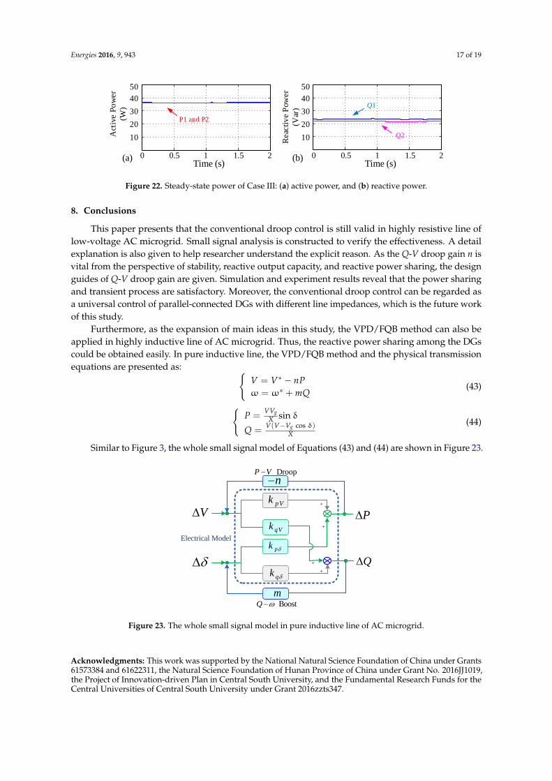
Energies 2016, 9, 943 17 of 19Energies 2016, 9, 943 17 of 19
50
40
30
20
10
0 0.5 1 1.5 2Time (s)
(a)
50
40
30
20
10
0 0.5 1 1.5 2Time (s)
(b)
Reac
tiv
e P
ow
er
(Var
)
Act
ive P
ow
er
(W)
P1 and P2
Q2
Q1
Figure 22. Steady-state power of Case III: (a) active power, and (b) reactive power.
8. Conclusions
This paper presents that the conventional droop control is still valid in highly resistive line of
low-voltage AC microgrid. Small signal analysis is constructed to verify the effectiveness. A detail
explanation is also given to help researcher understand the explicit reason. As the Q-V droop gain n
is vital from the perspective of stability, reactive output capacity, and reactive power sharing, the
design guides of Q-V droop gain are given. Simulation and experiment results reveal that the power
sharing and transient process are satisfactory. Moreover, the conventional droop control can be
regarded as a universal control of parallel-connected DGs with different line impedances, which is
the future work of this study.
Furthermore, as the expansion of main ideas in this study, the VPD/FQB method can also be
applied in highly inductive line of AC microgrid. Thus, the reactive power sharing among the DGs
could be obtained easily. In pure inductive line, the VPD/FQB method and the physical transmission
equations are presented as:
*
*
V V nP
mQ
(43)
sin
( cos )
g
g
VVP
X
V V VQ
X
(44)
Similar to Figure 3, the whole small signal model of Equations (43) and (44) are shown in Figure 23.
pVk
qVk
n
m
DroopP V
BoostQ
Electrical Model
P
Q
V
pk
qk
Figure 23. The whole small signal model in pure inductive line of AC microgrid.
Acknowledgments: This work was supported by the National Natural Science Foundation of China under
Grants 61573384 and 61622311, the Natural Science Foundation of Hunan Province of China under Grant No.
2016JJ1019, the Project of Innovation-driven Plan in Central South University, and the Fundamental Research
Funds for the Central Universities of Central South University under Grant 2016zzts347.
Figure 22. Steady-state power of Case III: (a) active power, and (b) reactive power.
8. Conclusions
This paper presents that the conventional droop control is still valid in highly resistive line oflow-voltage AC microgrid. Small signal analysis is constructed to verify the effectiveness. A detailexplanation is also given to help researcher understand the explicit reason. As the Q-V droop gain n isvital from the perspective of stability, reactive output capacity, and reactive power sharing, the designguides of Q-V droop gain are given. Simulation and experiment results reveal that the power sharingand transient process are satisfactory. Moreover, the conventional droop control can be regarded asa universal control of parallel-connected DGs with different line impedances, which is the future workof this study.
Furthermore, as the expansion of main ideas in this study, the VPD/FQB method can also beapplied in highly inductive line of AC microgrid. Thus, the reactive power sharing among the DGscould be obtained easily. In pure inductive line, the VPD/FQB method and the physical transmissionequations are presented as:
V = V∗ − nPω = ω∗ + mQ
(43)
P =
VVgX sin δ
Q =V(V−Vg cos δ)
X
(44)
Similar to Figure 3, the whole small signal model of Equations (43) and (44) are shown in Figure 23.
Energies 2016, 9, 943 17 of 19
50
40
30
20
10
0 0.5 1 1.5 2Time (s)
(a)
50
40
30
20
10
0 0.5 1 1.5 2Time (s)
(b)
Reac
tiv
e P
ow
er
(Var
)
Act
ive P
ow
er
(W)
P1 and P2
Q2
Q1
Figure 22. Steady-state power of Case III: (a) active power, and (b) reactive power.
8. Conclusions
This paper presents that the conventional droop control is still valid in highly resistive line of
low-voltage AC microgrid. Small signal analysis is constructed to verify the effectiveness. A detail
explanation is also given to help researcher understand the explicit reason. As the Q-V droop gain n
is vital from the perspective of stability, reactive output capacity, and reactive power sharing, the
design guides of Q-V droop gain are given. Simulation and experiment results reveal that the power
sharing and transient process are satisfactory. Moreover, the conventional droop control can be
regarded as a universal control of parallel-connected DGs with different line impedances, which is
the future work of this study.
Furthermore, as the expansion of main ideas in this study, the VPD/FQB method can also be
applied in highly inductive line of AC microgrid. Thus, the reactive power sharing among the DGs
could be obtained easily. In pure inductive line, the VPD/FQB method and the physical transmission
equations are presented as:
*
*
V V nP
mQ
(43)
sin
( cos )
g
g
VVP
X
V V VQ
X
(44)
Similar to Figure 3, the whole small signal model of Equations (43) and (44) are shown in Figure 23.
pVk
qVk
n
m
DroopP V
BoostQ
Electrical Model
P
Q
V
pk
qk
Figure 23. The whole small signal model in pure inductive line of AC microgrid.
Acknowledgments: This work was supported by the National Natural Science Foundation of China under
Grants 61573384 and 61622311, the Natural Science Foundation of Hunan Province of China under Grant No.
2016JJ1019, the Project of Innovation-driven Plan in Central South University, and the Fundamental Research
Funds for the Central Universities of Central South University under Grant 2016zzts347.
Figure 23. The whole small signal model in pure inductive line of AC microgrid.
Acknowledgments: This work was supported by the National Natural Science Foundation of China under Grants61573384 and 61622311, the Natural Science Foundation of Hunan Province of China under Grant No. 2016JJ1019,the Project of Innovation-driven Plan in Central South University, and the Fundamental Research Funds for theCentral Universities of Central South University under Grant 2016zzts347.

Energies 2016, 9, 943 18 of 19
Author Contributions: Xiaochao Hou conceived the main idea and wrote the manuscript with guidance fromYao Sun and Hua Han. Wenbin Yuan and Chaolu Zhong performed the experiments; and Josep M. Guerreroreviewed the work and gave helpful improvement suggestions.
Conflicts of Interest: The authors declare no conflict of interest.
References
1. Lasseter, R.H.; Paigi, P. Microgrid: A conceptual solution. In Proceedings of the 2004 IEEE Power ElectroSpecial Conference, Aachen, Germany, 20–25 June 2004; pp. 4285–4290.
2. Yan, B.; Wang, B.; Zhu, L. A novel, stable, and economic power sharing scheme for an autonomous microgridin the energy internet. Energies 2015, 8, 12741–12764. [CrossRef]
3. Ahn, C.; Peng, H. Decentralized and real-time power dispatch control for an islanded microgrid supportedby distributed power sources. Energies 2013, 6, 6439–6454. [CrossRef]
4. Golsorkhi, M.S.; Lu, D.D.C. A control method for inverter-based islanded microgrids based on V-I droopcharacteristics. IEEE Trans. Power Deliv. 2015, 30, 1196–1204. [CrossRef]
5. Pogaku, N.; Prodanovic, M.; Green, T.C. Modeling, analysis and testing of autonomous operation ofan inverter-based microgrid. IEEE Trans. Power Electron. 2007, 22, 613–625. [CrossRef]
6. He, J.W.; Li, Y.; Bosnjak, D.; Harris, B. Investigation and active damping of multiple resonances ina parallel-inverter-based microgrid. IEEE Trans. Power Electron. 2013, 28, 234–246. [CrossRef]
7. Abdelaziz, M.M.A.; Shaaban, M.F.; Farag, H.E.; El-Saadany, E.F. A multistage centralized control scheme forislanded microgrids with PEV. IEEE Trans Sustain. Energy 2014, 5, 927–937. [CrossRef]
8. Song, N.O.; Lee, J.H.; Kim, H.M.; Im, Y.H.; Lee, J.Y. Optimal energy management of multi-microgrids withsequentially coordinated operations. Energies 2015, 8, 8371–8390. [CrossRef]
9. Caldognetto, T.; Paolo, T. Microgrids operation based on master-slave cooperative control. IEEE J. Emerg. Sel.Top. Power Electron. 2014, 2, 1081–1088. [CrossRef]
10. Sun, Y.; Zhong, C.; Hou, X.; Yang, J.; Han, H.; Guerrero, J.M. Distributed cooperative synchronization strategyfor multi-bus microgrids. Int. J. Electr. Power Energy Syst. 2017, 86, 18–28. [CrossRef]
11. Lim, Y.; Kim, H.M.; Kinoshita, T. Distributed load-shedding system for agent-based autonomous microgridoperations. Energies 2014, 7, 385–401. [CrossRef]
12. Yu, Z.; Ai, Q.; Gong, J.; Piao, L. A novel secondary control for microgrid based on synergetic control ofmulti-agent system. Energies 2016, 9. [CrossRef]
13. Chandorkar, M.C.; Divan, D.M.; Adapa, R. Control of parallel connected inverters in standalone AC supplysystems. IEEE Trans. Ind. Appl. 1993, 29, 136–143. [CrossRef]
14. Yu, X.; Khambadkone, A.M.; Wang, H. Control of parallel-connected power converters for low-voltagemicrogrid—Part I: A hybrid control architecture. IEEE Trans. Power Electron. 2010, 25, 2962–2970. [CrossRef]
15. Tuladhar, A.; Jin, H.; Unger, T.; Mauch, K. Control of parallel inverters in distributed ac power systems withconsideration of line impedance effect. IEEE Trans. Ind. Appl. 2000, 36, 131–138. [CrossRef]
16. Guerrero, J.M.; Matas, J.; de Vicuña, L.G. Decentralized control for parallel operation of distributed generationinverters using resistive output impedance. IEEE Trans. Ind. Electron. 2007, 54, 994–1004. [CrossRef]
17. Han, H.; Hou, X.; Yang, J.; Wu, J.; Su, M.; Guerrero, J.M. Review of power sharing control strategies forislanding operation of AC microgrids. IEEE Trans. Smart Grid 2016, 7, 200–215. [CrossRef]
18. Zhong, Q.-C. Robust droop controller for accurate proportional load sharing among inverters operated inparallel. IEEE Trans. Ind. Electron. 2013, 60, 1281–1290. [CrossRef]
19. Zhong, Q.-C.; Hornik, T. Control of Power Inverters in Renewable Energy and Smart Grid Integration; Wiley-IEEEPress: Hoboken, NJ, USA, 2013.
20. He, J.; Li, Y. Analysis, design, and implementation of virtual impedance for power electronics interfaceddistributed generation. IEEE Trans. Ind. Appl. 2011, 47, 2525–2538. [CrossRef]
21. Guerrero, J.M.; Vicuna, L.G.D.; Matas, J.; Castilla, M.; Miret, J. Output impedance design of parallel-connectedUPS inverters with wireless load-sharing control. IEEE Trans. Ind. Electron. 2005, 52, 1126–1135. [CrossRef]
22. Li, Y.W.; Kao, C.-N. An accurate power control strategy for power-electronics-interfaced distributedgeneration units operating in a low-voltage multibus microgrid. IEEE Trans. Power Electron. 2009, 24,2977–2988.

Energies 2016, 9, 943 19 of 19
23. Guerrero, J.M.; Vasquez, J.C.; Matas, J.; de Vicuna, L.G.; Castilla, M. Hierarchical control of droop-controlledAC and DC microgrids—A general approach toward standardization. IEEE Trans. Ind. Electron. 2011, 58,158–172. [CrossRef]
24. Parhizi, S.; Lotfi, H.; Khodaei, A.; Bahramirad, S. State of the art in research on microgrids: A review.IEEE Access 2015, 3, 890–925. [CrossRef]
25. Bevrani, H.; Shokoohi, S. An intelligent droop control for simultaneous voltage and frequency regulation inislanded microgrids. IEEE Trans. Smart Grid 2013, 4, 1505–1513. [CrossRef]
26. Majumder, R.; Ledwich, G.; Ghosh, A. Droop control of converter-interfaced microsources in rural distributedgeneration. IEEE Trans. Power Deliv. 2010, 25, 2768–2778. [CrossRef]
27. Majumder, R.; Chaudhuri, B.; Ghosh, A. Improvement of stability and load sharing in an autonomousmicrogrid using supplementary droop control loop. IEEE Trans. Power Syst. 2010, 25, 796–808. [CrossRef]
28. Heuck, K.; Dettmann, K.D.; Reuter, E. Elektrische Energieversorgung; Vieweg: Berlin, Germany, 1991.(In German)
29. Engler, A.; Soultanis, N. Droop control in LV-grids. In Proceedings of the 2005 International Conference onFuture Power Systems, Amsterdam, The Netherlands, 16–18 November 2005.
30. Mohamed, Y.; El-Saadany, E.F. Adaptive decentralized droop controller to preserve power sharing stabilityof paralleled inverters in distributed generation microgrids. IEEE Trans. Power Electron. 2008, 23, 2806–2816.[CrossRef]
31. Sao, C.K.; Lehn, P.W. Autonomous load sharing of voltage source converters. IEEE Trans. Power Deliv. 2005,20, 1009–1016. [CrossRef]
32. Shintai, T.; Miura, Y.; Ise, T. Oscillation damping of a distributed generator using a virtual synchronousgenerator. IEEE Trans. Power Deliv. 2014, 29, 668–676. [CrossRef]
33. Jan, M.; Janusz, W.B.; James, R.B. Power System Dynamics: Stability, and Control; Wiley: Chichester, UK, 2008.34. Rokrok, E.; Golshan, M.E.H. Adaptive voltage droop scheme for voltage source converters in an islanded
multi-bus microgrid. IET Gener. Transm. Distrib. 2010, 4, 562–578. [CrossRef]35. Mahmood, H.; Michaelson, D.; Jiang, J. Reactive power sharing in islanded microgrids using adaptive
voltage droop control. IEEE Trans. Smart Grid 2015, 6, 3052–3060. [CrossRef]36. He, J.; Li, Y.W. An enhanced microgrid load demand sharing strategy. IEEE Trans. Power Electron. 2012, 27,
3984–3995. [CrossRef]37. Lee, C.T.; Chu, C.C.; Cheng, P.T. A new droop control method for the autonomous operation of distributed
energy resource interface converters. IEEE Trans. Power Electron. 2013, 28, 1980–1993. [CrossRef]38. Han, H.; Liu, Y.; Sun, Y.; Su, M.; Guerrero, J.M. An improved droop control strategy for reactive power
sharing in islanded microgrid. IEEE Trans. Power Electron. 2015, 30, 3133–3141. [CrossRef]39. Zhu, Y.; Zhuo, F.; Wang, F.; Liu, B.; Gou, R.; Zhao, Y. A virtual impedance optimization method for reactive
power sharing in networked microgrid. IEEE Trans. Power Electron. 2016, 31, 2890–2904. [CrossRef]40. Mahmood, H.; Michaelson, D.; Jiang, J. Accurate reactive power sharing in an islanded microgrid using
adaptive virtual impedances. IEEE Trans. Power Electron. 2015, 30, 1605–1617. [CrossRef]41. Milczarek, A.; Malinowski, M.; Guerrero, J.M. Reactive power management in islanded microgrid— Proportional
power sharing in hierarchical droop control. IEEE Trans. Smart Grid 2015, 6, 1631–1638. [CrossRef]
© 2016 by the authors; licensee MDPI, Basel, Switzerland. This article is an open accessarticle distributed under the terms and conditions of the Creative Commons Attribution(CC-BY) license (http://creativecommons.org/licenses/by/4.0/).